Communication

CdTe Nanocrystal Hetero-Junction Solar Cells with High Open Circuit Voltage Based on Sb-doped TiO2 Electron Acceptor Materials

1
School of Materials Science and Engineering, South China University of Technology, Guangzhou 510640, China
2
Institute of Polymer Optoelectronic Materials & Devices, State Key Laboratory of Luminescent Materials & Devices, South China University of Technology, Guangzhou 510640, China
3
Siyuan Laboratory, Guangzhou Key Laboratory of Vacuum Coating Technologies and New Energy Materials, Department of Physics, Jinan University, Guangzhou 510632, China
*
Authors to whom correspondence should be addressed.
Nanomaterials 2017, 7(5), 101; https://doi.org/10.3390/nano7050101
Submission received: 13 April 2017 / Revised: 27 April 2017 / Accepted: 28 April 2017 / Published: 3 May 2017

Abstract

:
We propose Sb-doped TiO2 as electron acceptor material for depleted CdTe nanocrystal (NC) hetero-junction solar cells. Novel devices with the architecture of FTO/ZnO/Sb:TiO2/CdTe/Au based on CdTe NC and TiO2 precursor are fabricated by rational ambient solution process. By introducing TiO2 with dopant concentration, we are able to tailor the optoelectronic properties of NC solar cells. Our novel devices demonstrate a very high open circuit voltage of 0.74 V, which is the highest Voc reported for any CdTe NC based solar cells. The power conversion efficiency (PCE) of solar cells increases with the increase of Sb-doped content from 1% to 3%, then decreases almost linearly with further increase of Sb content due to the recombination effect. The champion device shows Jsc, Voc, FF, and PCE of 14.65 mA/cm2, 0.70 V, 34.44, and 3.53% respectively, which is prospective for solution processed NC solar cells with high Voc.

1. Introduction

Nanocrystal (NC) solar cells have received extensive attention in the last several years due to their many advantages—such as low cost, environmental friendliness, solution process, simple device technics, and compatible roll-to-roll manufacturing [1,2,3,4,5,6,7,8]. The most efficient NC based solar cells nowadays are fabricated by using CdTe or PbS NC as donors with wide bandgap semiconductor materials as acceptors [9,10,11,12,13]. Compared to PbS NC, CdTe NC is less complex and more stable in air, which permits devices to be fabricated under ambient conditions. Thus, CdTe NC thin film has been studied intensively [14,15,16,17,18,19,20]. The working principle of efficient CdTe NC solar cells is based on the p-n heterojunction that contains two media: an electron donor and electron acceptor. To prepare a high quality CdTe NC donor absorber, a layer by layer sintering process should be carried out to eliminate stress and defects in CdTe NC thin film [21,22]. The electron acceptor materials—typically ZnO, CdSe or other n-type semiconductor thin films—are thus the key to improve the device performance. The most efficient CdTe NC–ZnO solar cells are fabricated by using a normal structure of ITO/CdTe/ZnO/Al [10]. In this device architecture, Zn2+ precursor is deposited on the CdCl2 treated CdTe NC thin film and annealed at a moderate temperature of 300 °C, which enables high quality junction formation and avoids large current leaks. However, efforts try to duplicate this device with an inverted structure of ITO/ZnO/CdTe/Au failed due to the poor junction quality in the ZnO–CdTe interface, which had been confirmed in our previous work [23]. It is noted that there are many merits for solar cells with inverted structure, such as a charge separating interface close to the illumination and usage of metal or metal oxide with high work function as a hole-collecting electrode, which endows device long lifetime. Solution processed CdTe NC based solar cells with inverted structure of ITO/CdSe/CdTe/Au were reported for the first time by Towsend et al. [19]. Although as high as 3.8% PCE was obtained in the above devices, they suffered from low Voc (< 0.5 V) value, much lower than that (up to 0.8 V) of CdTe/CdS devices prepared by close space sublimation (CSS) method [24]. With Cr/Au as hole collecting electrode, the Voc of devices with the structure of ITO/CdSe/CdTe/Cr/Au can be further increased to 0.62 V [20]. By using ZnO as the interlayer, devices with an architecture of ITO/ZnO/CdSe/CdTe/Au obtain a high Voc of up to 0.6 V in conjunction with a high PCE of ~6% reported in our recent work [25,26]. Recently, Yang et al. [27,28] developed an in situ route to construct CdTe–CdS NC bulk heterostructure solar cells by direct thermal treatment of mercaptoethylamine stabilized CdTe NC. In this device structure, the formation of n-CdS shells on CdTe NC eliminated the recombination of carrier and improved the device performance. Recently, [29] introduced p type spiro-OMeTAD as the hole transport layer between CdTe NC thin film and Au electrode, as high as 0.71 V of Voc was obtained, which was the highest Voc value ever reported for solution-processed CdTe NC based solar cells. Another way to improve the Voc of CdTe NC based solar cells is to engineer the bandgap structure of the photo-generated electron-accepting materials. As previously reported [12], the trap state density of CdTe was 1014 cm−3, high doped density of n-type materials was necessary to fully deplete the CdTe NC film in order to increase the carriers’ separating and collecting efficiencies. It had been found that, by using n type doped TiO2 as the electron acceptor, the performance of PbS colloidal quantum dot/TiO2 heterojunction solar cells can be tailored and improved substantially [30]. Bulk hetero-junction structure was built as porous structure formed during the decomposition of Ti-sol, which improved carrier collecting efficiency. Herein, we introduce solution-processed CdTe NC/TiO2 hetero-junction solar cells consisting of ZnO film, thermal decomposition Sb-doped TiO2 film, and solution processed CdTe NC thin film. The carrier separating/collecting efficiency of solar cells can be improved by introducing Sb-doped in TiO2 as the electron acceptor. It is found that Voc up to 0.7 V can be obtained with a Sb-doped TiO2 electrode and as high as 0.74 V is obtained in the case of 8% Sb-doped TiO2 devices, which is the highest Voc ever reported for solution-processed CdTe NC based solar cells.

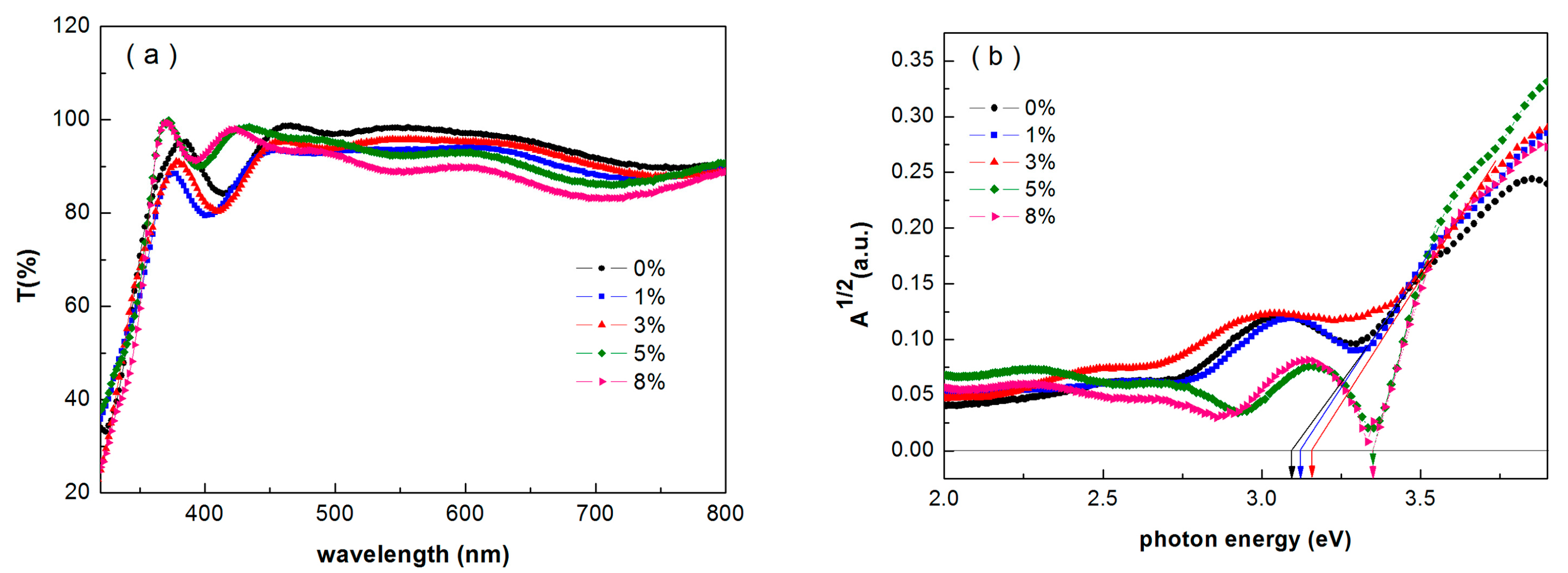
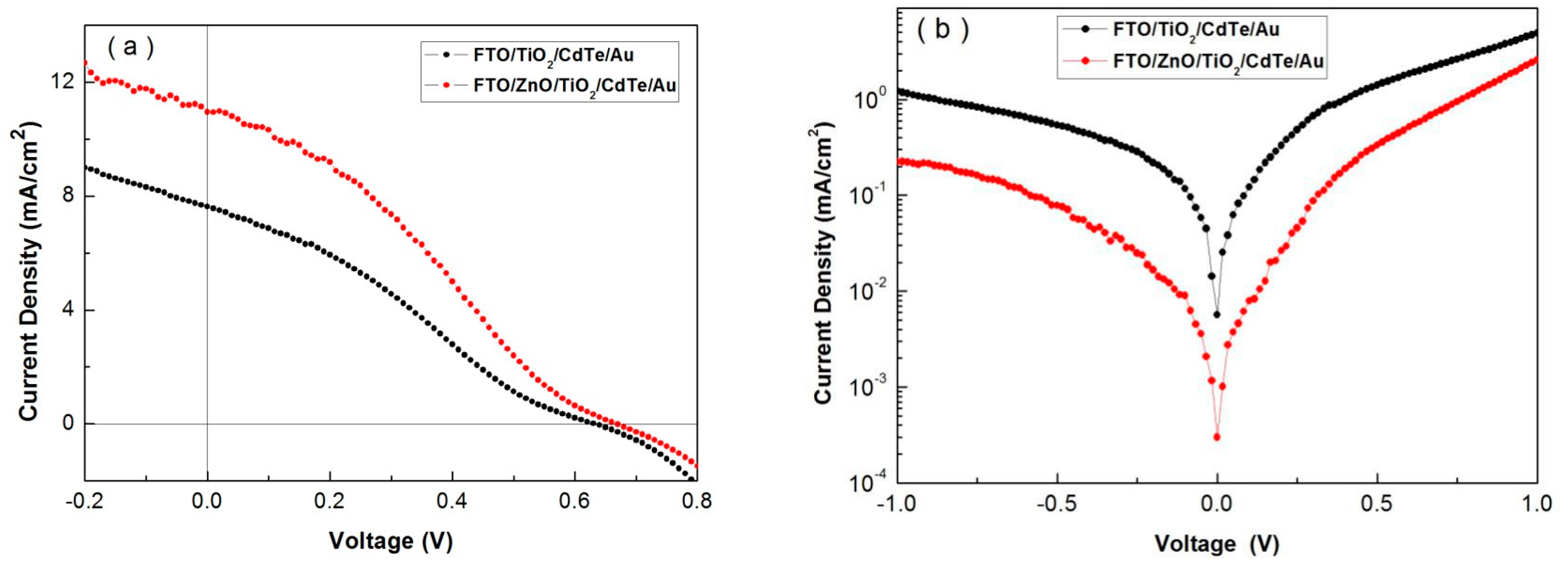
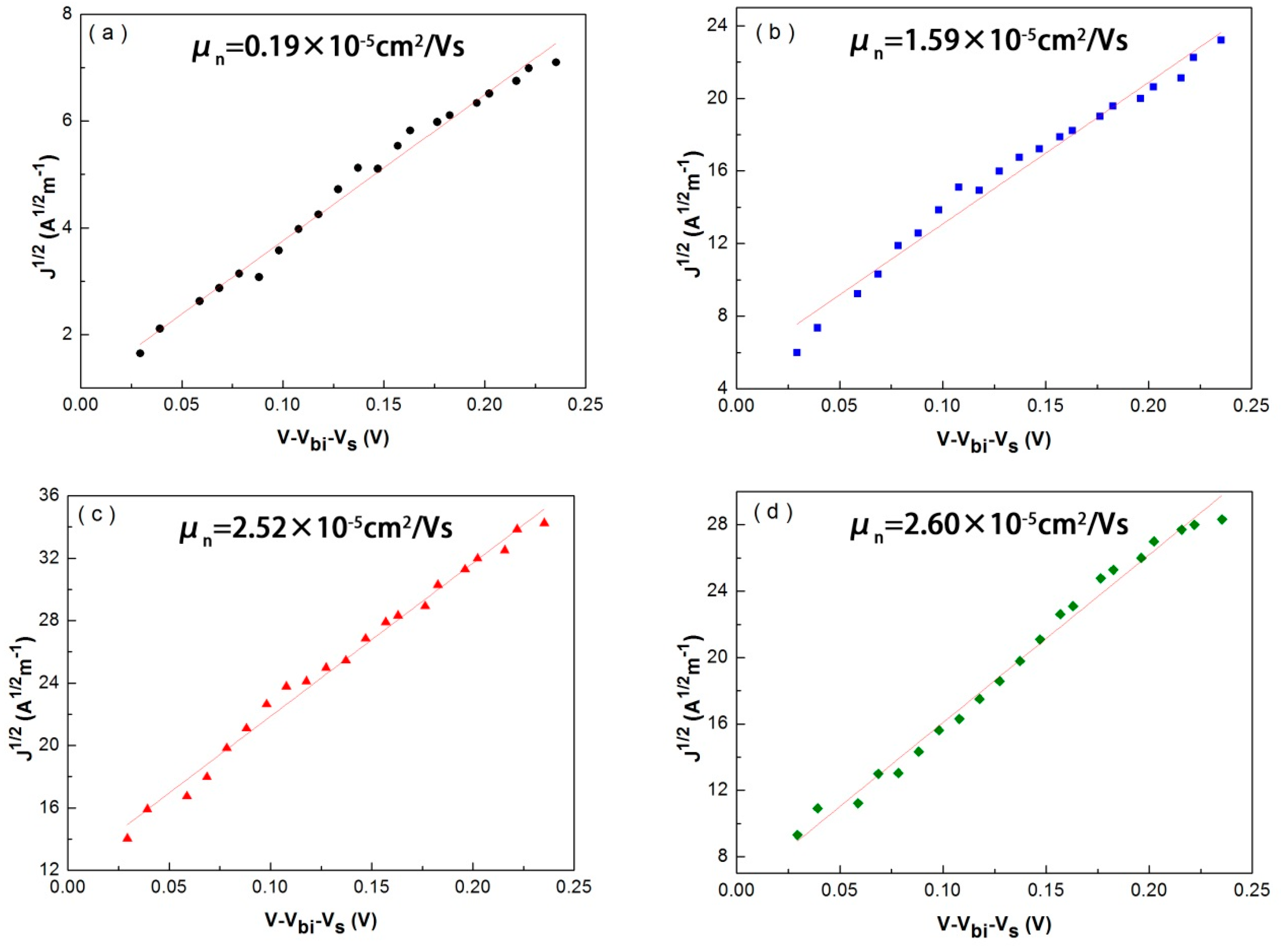
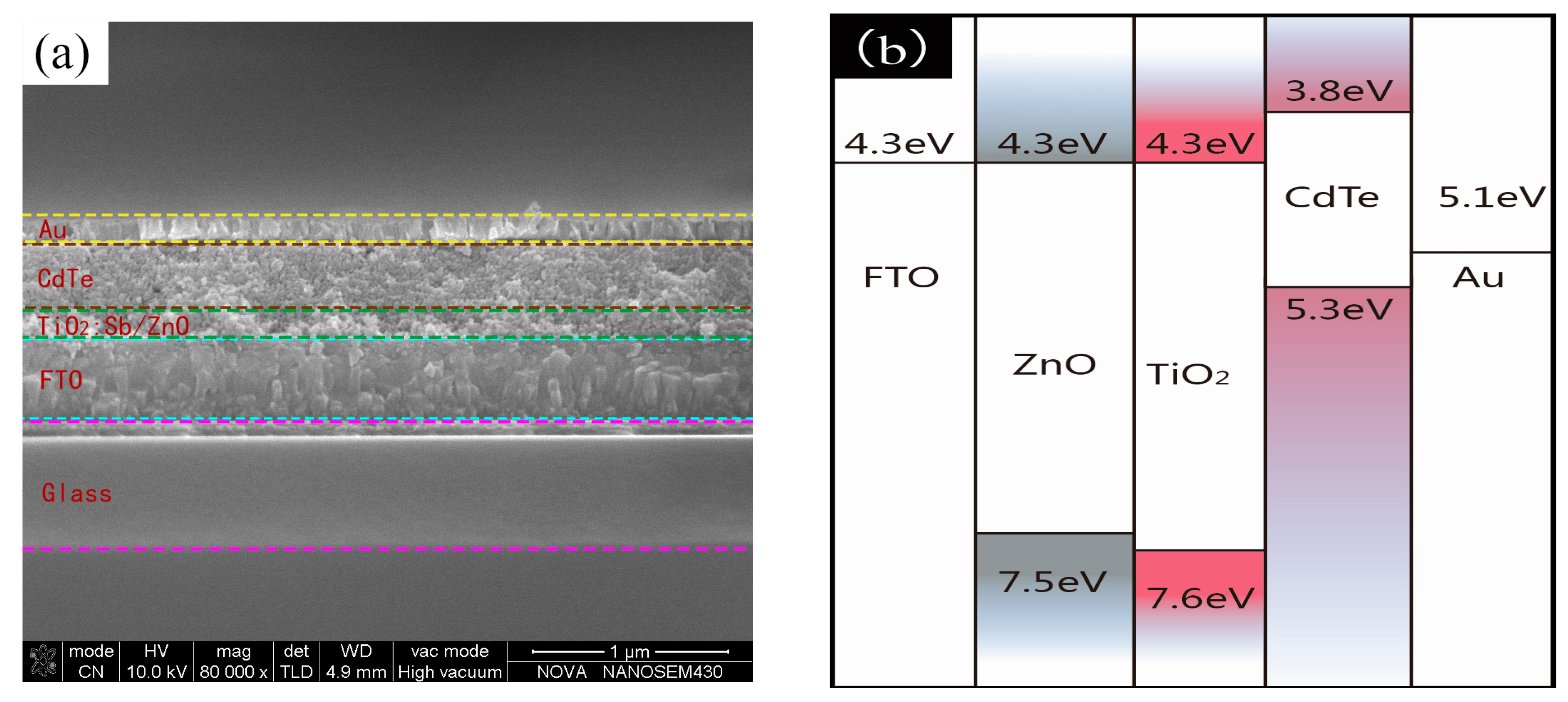
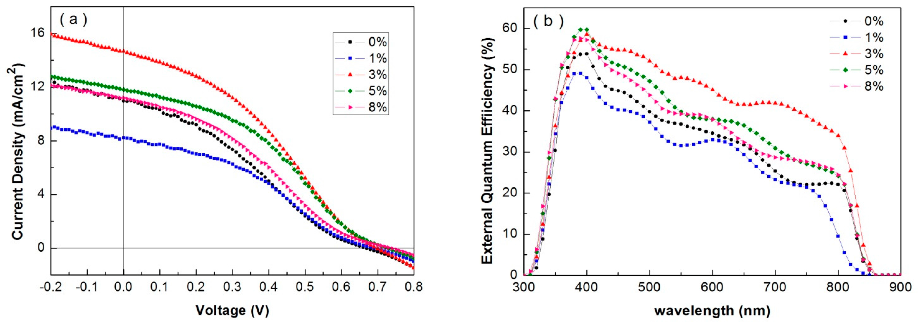
2. Results and Discussion

In the case of inverted structure CdTe NC based solar cells, the absorbance or transmission of window layers has a great effect on the light passing through the CdTe NC active layer. Window layers with a high light transmission in short wavelengths will increase the response of spectrum in the device. Figure 1 shows the transmission spectra and the root mean square of the absorption against photon energy of Sb-doped TiO2. The measurement is taken by using FTO as the standard sample. From Figure 1a, it can be seen that the FTO/ZnO/Sb-TiO2 thin films block the light with a wavelength shorter than 400 nm and show almost transparent behavior for wavelengths from 400 to 1000 nm. A little decrease in the transmission is found when the Sb doping concentration increases to 8%. As shown in Figure 1b, the bandgap of the Sb-doped TiO2 layer utilized in this work is in the range of 3.1–3.3 eV, which is derived by taking a tangent of straight line of this curve at A = 0 (A = (αhν)). There are almost no changes with different Sb doping ratios, which imply that Sb doping does not change the bandgap of TiO2 thin film, in accordance with the previous report [30].
To build solar cells devices, we deposited five layers of CdTe NC thin film on 50 nm Sb-doped TiO2 and 40 nm-thick ZnO thin film. Au is deposited on the CdTe layer to make ohmic contact. The cross-sectional SEM micrograph of this CdTe–TiO2 device is also depicted in Figure 2a. The CdTe NC film is homogeneous with thickness ~400 nm. The band alignment of solar cells is presented in Figure 2b. Photoelectrons are generated in the CdTe NC active layer and separated in the CdTe/TiO2 interface. The electrons are transported to ZnO and collected by the FTO, while photogenerated holes traveled to the Au electrode.
The presented ZnO thin film can provide better electrical stability and the smooth and pin-hole free TiO2 film can be grown on it, which is confirmed in our previous work [25,26]. Furthermore, it can eliminate catastrophic shorts from the upper contact directly through CdTe layers to the FTO. For comparison, devices with structures of FTO/ZnO/TiO2/CdTe/Au and FTO/TiO2/CdTe/Au are fabricated under the same conditions, that is, all devices consist of 50 nm TiO2 and 400 nm CdTe active layers. The current density versus voltage (JV) characteristics of these devices under 1000 Wm−2 (AM 1.5 G) are shown in Figure 3a, while the dark JV curves are presented in Figure 3b. The Jsc, Voc, FF, and PCE values of the devices are summarized in Table 1. It is found that without ZnO film, the dark current is large. On the contrary, devices with a ZnO interlayer show good diode properties. The Jsc, Voc, FF and PCE values of devices with the ZnO interlayer are 10.95 mA/cm2, 0.66 V, 30.35 and 2.22% respectively, while these values for devices without the ZnO interlayer are 7.62 mA/cm2, 0.63 V, 28.53, and 1.37%. We suppose that TiO2 deposited directly on the FTO substrate contains high interface defect density which can lead to high dark current and result in low device performance, confirming our previous work on ITO/ZnO/CdSe/CdTe/Au devices [26].
It was reported that the conduction band edge of Sb-doped TiO2 is −4.22 eV, while this value is −3.81 eV for undoped TiO2 [30]. The conduction band edge value of Sb-doped TiO2 is lower than that of CdTe film (−4.0 eV), which is promising for photo electron injecting to the conduction band of TiO2. To investigate the effect of different Sb doping contents on device performance, we fabricated CdTe NC based solar cells with different Sb contents of 1, 3, 5, and 8% (w/w). Current density vs. voltage characteristics under AM 1.5 G illumination are shown in Figure 4a, and the device performances are listed in Table 2. The control devices (using undoped TiO2) shows a Voc of 0.66 V and PCE of 2.22%, while all Sb-doped TiO2 devices show higher Voc. Similar device performance is obtained in the case of low Sb-doped TiO2 device. The PCE of device increases linearly from 1% to 3% Sb-doped content, then decreases with the further increase of Sb-doped content from 3% to 8%. The best device performance is obtained in the case of 3% (w/w) Sb-doped TiO2 electrodes. The Jsc, Voc, FF, and PCE values of device are 14.65 mA/cm2, 0.70 V, 34.44, and 3.53% respectively. The PCE value of the 3% (w/w) Sb-doped device is 50 % higher than that of the control device, mainly arising from the increase in Voc and Jsc. Compared to the controlled devices, 3% or 5% Sb-doped TiO2 devices show higher Voc coupled with higher PCE up to 3%. The EQE spectra (Figure 4b) show that all Sb-doped TiO2 devices have higher EQE almost across the entire absorbing region compared to undoped TiO2 devices. This suggests that the transfer of photogenerated carriers in the Sb-doped devices is more effective than that in undoped devices. It is noted that the Voc is up to 0.69 V with different Sb-doped devices and as high as 0.74 V is obtained in the case of 8% Sb-doped device. This is, to the best our knowledge, the highest Voc reported for solution processed CdTe NC based solar cells. However, the PCE is decreased to 2.49% for 8% Sb-doped device. We suppose that, in the case of high Sb-doped TiO2, excess Sb may act as recombination center for carrier, which will render the Jsc of device. It is also noted that “roll over” phenomena appear in the JV curves for different CdTe-TiO2 solar cells device, which may come from large series resistance of CdTe NC film. We believe that the low FF is mainly derived from low quality of CdTe NC thin film. The compactness, morphology, and grain size of CdTe NC is greatly affected by the substrate materials even all the same parameter for processing CdTe NC film. As CdTe and CdSe NCs have similar sizes and structures (zinc-blende or wurtzite), the lattice mismatch between CdTe and CdSe is very small. High quality CdTe NC film can be obtained with CdSe NC as interlayer and high solar cells performance is expected in this case, which has been confirmed in our previously reports [25,26]. However, when CdTe NCs are deposited on FTO/ZnO/TiO2 by a layer-by-layer sintering process, low quality CdTe NC film with pinholes or other defects will be obtained as the lattice mismatch between CdTe and TiO2. The contact between CdTe and Au is non ohmic due to the large resistance existed in CdTe NC thin film, then JV curves with cross over behavior are likely observed in this case. The principal path to CdTe NC-TiO2 solar cells’ further improvement lies in continued reductions in electronic trap state densities in the junction, improving the quality of CdTe NC film and optimizing the contact for CdTe NC film.
To investigate the mobility of TiO2 with dopant concentrations, we deposit TiO2 on the FTO substrate and use Al as the contact electrodes. As shown in Figure 5, the electron mobility is calculated by the formula of J = 9 8 ε μ n V 2 L 3 [13], where ε is the relative dielectric constant, Vbi is the potential difference between FTO and TiO2 (Vbi = 0.1 V in this case), Vs is the applied voltage, L is the thickness of the TiO2 active layer (~50 nm in this case). In the case of undoped TiO2, it shows a relative low electron mobility of 0.19 × 105 cm2 V−1 s−1, which implies that large surface states exist in the film. The electron mobility increases with the Sb-doped content increase linearly (as 8% and 5% Sb-doped TiO2 have similar mobility the JV curve for 8% Sb-doped TiO2 is not presented here). The mobility of TiO2 film has a great effect on the performance of NC based solar cells. Film with a high mobility may markedly reduce the recombination of electrons and holes during the transfer of carriers and a high Jsc is expected to be obtained in this case, which is consistent with our JV curve measurement of CdTe NC based solar cells with different Sb-doped TiO2 electrodes (see Table 2).

3. Materials and Methods

The preparation of TiO2-sol with different Sb contents was carried out under ambient conditions. In a typical 3% (w/w) Sb-doped TiO2 precursor, titanium n-butoxide (4.25 mL) was mixed with ethanolamine (3.75 mL) and ethyl alcohol (25 mL) in a beaker under continuous stirred for 2 h. 5 mL acetic acid, 5 mL deionized water, and 8.33 uL antimony(III) ethoxide (with Sb to Ti = 1:20) were added into the mixture and placed in a fume hood to allow condensation reactions. After three days, the volume of Ti-sols was about 15 mL. The Ti-sols were then transferred into a clean vial for TiO2 film fabrication. By varying the ratio of Sb2+ to titanium n-butoxide in the mixture, we obtained Ti-sol with dopant concentration. The fabrication of ZnO precursor and CdTe NC could be found in our previous reports [25,31].
The CdTe NC based solar cells with FTO/ZnO/TiO2:Sb/CdTe/Au structures were fabricated by a layer-by-layer solution process. Firstly, the ZnO precursor was spin-coated on FTO at a speed of 3000 rpm for 20 s. Then the sample was annealed at 200 °C for 10 min and then 400 °C for 10 min. Several drops of the Ti-sols were deposited on the FTO/ZnO substrates by spin coating at 2500rpm for 15 s. The sample was immediately transferred to a hot plate at 500 °C for 60 min. The deposition of CdTe film can be found in our previous report [25]. The final products were annealed at 400 °C for 15 min. Au with 80 nm thickness was deposited on the CdTe film via thermal evaporation to make back contact.

4. Conclusions

In conclusion, we demonstrated that inverted CdTe NC based solar cells fabricated with different Sb-doped TiO2 electrodes have many benefits such as simple structure, easy control, less interface defects, high electron mobility, and ideal band offsets for carrier separation, which results in good device performance. In the case of 3% Sb-doped TiO2 device, we obtain a high Voc up to 0.7 V with PCE of 3.53%. Voc as high as 0.74 V is obtained in the case of an 8% Sb-doped device. The Sb doping ratio is found to have great effect on the device performance. Our results imply that if a CdTe layer, a Sb-doped TiO2 layer, and their junction undergo more optimized processing (such as increasing annealing temperature or annealing time), the device performance can be further increased. This exploration gives more insight into solution processed CdTe NC based solar cells with Sb-doped TiO2 electrodes.

Acknowledgments

We are thankful the financial support of the National Natural Science Foundation of China (Nos. 91333206, 61274062 and 11204106), National Science Foundation for Distinguished Young Scholars of China (Grant No. 51225301), Guangdong Province Natural Science Fund (No. 2014A030313257), National Undergraduate Innovative and Entrepreneurial Training Program (No. 201610561070) and the Fundamental Research Funds for the Central Universities.

Author Contributions

Donghuan Qin and Miaozi Li conceived and designed the experiments; Miaozi Li, Xinyan Liu, Shiya Wen, Songwei Liu and Jingxuan Heng performed the experiments; Wei Xu and Miaozi Li analyzed the data; Lintao Hou, Wenbo Huang, Hongbin Wu and Miaozi Li contributed reagents/materials/analysis tools; Donghuan Qin and Miaozi Li wrote the paper. Authorship must be limited to those who have contributed substantially to the work reported.

Conflicts of Interest

The authors are declared no conflict of interest.

References

  1. Kagan, C.R.; Lifshitz, E.; Sargent, E.H.; Talapin, D.V. Building devices from colloidal quantum dots. Science 2016, 353, aac5523. [Google Scholar] [CrossRef] [PubMed]
  2. Lan, X.Z.; Voznyy, O.; Kiani, A.; de Arquer, F.P.G.; Abbas, A.S.; Kim, G.H.; Liu, M.X.; Yang, Z.Y.; Walters, G.; Xu, J.X.; et al. Passivation using molecular halides increases quantum dot solar cell performance. Adv. Mater. 2016, 28, 299–304. [Google Scholar] [CrossRef] [PubMed]
  3. Lan, X.Z.; Voznyy, O.; de Arquer, F.P.G.; Liu, M.; Xu, J.X.; Proppe, A.H.; Walters, G.; Fan, F.J.; Tan, H.R.; Liu, M.; et al. 10.6% Certified colloidal quantum dot solar cells via solvent-Polarity-Engineered halide passivation. Nano Lett. 2016, 16, 4630–4634. [Google Scholar] [CrossRef] [PubMed]
  4. Xue, H.; Wu, R.; Xie, Y.; Tan, Q.; Qin, D.; Wu, H.; Huang, W. Recent progress on Solution-Processed CdTe nanocrystals solar cells. Appl. Sci. 2016, 6, 197. [Google Scholar] [CrossRef]
  5. Halim, M.A. Harnessing sun’s energy with quantum dots based next generation solar cell. Nanomaterials 2013, 3, 22–47. [Google Scholar] [CrossRef] [PubMed]
  6. Wei, J.; Xiong, Q.Y.; Mahpeykar, S.M.; Wang, X.H. Numerical study of complementary nanostructures for light trapping in colloidal quantum dot solar cells. Nanomaterials 2016, 6, 55. [Google Scholar] [CrossRef] [PubMed]
  7. Yuan, C.Z.; Li, L.; Huang, J.; Ning, Z.J.; Sun, L.C.; Agren, H. Improving the photocurrent in Quantum-Dot-Sensitized solar cells by employing alloy PbxCd1-xS quantum dots as photosensitizers. Nanomaterials 2016, 6, 97. [Google Scholar] [CrossRef] [PubMed]
  8. Chen, G.; Ning, Z.; Agren, H. Nanostructured Solar Cells. Nanomaterials 2016, 6, 145. [Google Scholar] [CrossRef] [PubMed]
  9. Kang, Y.J.; Yang, P.D.; Markovic, N.M.; Stamenkovic, V.R. Shaping electrocatalysis through tailored nanomaterials. Nano Today 2016, 11, 587–600. [Google Scholar] [CrossRef]
  10. Panthani, M.G.; Kurley, J.M.; Crisp, R.W.; Dietz, T.C.; Ezzyat, T.; Luthur, J.M.; Talapin, D.V. High efficiency solution processed sintered CdTe nanocrystal solar cells: The role of interfaces. Nano Lett. 2014, 14, 670–675. [Google Scholar] [CrossRef] [PubMed]
  11. Crisp, R.W.; Panthani, M.G.; Rance, W.L.; Duenow, J.N.; Parilla, P.A.; Callahan, R.; Dabney, M.S.; Berry, J.J.; Talapin, D.V.; Luther, J.M. Nanocrystal grain growth and device architectures for high-efficiency CdTe Ink-Based photovoltaics. ACS. Nano 2014, 8, 9063. [Google Scholar] [CrossRef] [PubMed]
  12. Jasieniak, J.; MacDonald, B.I.; Wakins, S.E.; Mulvaney, P. Solution-processed sintered nanocrystal solar cells via Layer-by-Layer assembly. Nano Lett. 2011, 11, 2856–2864. [Google Scholar] [CrossRef] [PubMed]
  13. Yang, Y.; Zhao, B.; Gao, Y.; Liu, H.; Tian, Y.; Qin, D.; Wu, H.; Hou, L.; Huang, W. Novel hybrid ligands for passivating PbS colloidal quantum dots to enhance the performance of solar cells. Nano-Micro Lett. 2015, 7, 325–331. [Google Scholar] [CrossRef]
  14. Chen, Z.; Zhang, H.; Du, X.; Cheng, X.; Chen, X.; Jiang, Y.; Yang, B. From planar-heterojunction to n-i structure: An efficient strategy to improve short-circuit current and power conversion efficiency of aqueous-solution-processed hybrid solar cells. Energy Environ. Sci. 2013, 6, 1597–1603. [Google Scholar] [CrossRef]
  15. Du, X.; Chen, Z.; Li, Z.; Hao, H.; Zeng, Q.; Dong, C.; Yang, B. Dip-Coated Gold Nanoparticle Electrodes for Aqueous-Solution-Processed Large-Area Solar Cells. Adv. Energy Mater. 2014, 4, 1400135. [Google Scholar] [CrossRef]
  16. Chen, Z.; Zhang, H.; Li, Z.; Hao, H.; Zeng, Q.; Wang, Y.; Du, X.; Wang, L.; Yang, B. In situ construction of nanocrystal CdTe-CdS bulk heterojunctions for inorganic nanocrystal solar cells. Adv. Energy Mater. 2014, 4, 1400235. [Google Scholar] [CrossRef]
  17. Anderson, I.E.; Breeze, A.J.; Olson, J.D.; Yang, L.; Sahoo, Y.; Cater, S.A. ALL-inorganic spin-cast nanoparticle solar cells with nonselective electrodes. Appl. Phys. Lett. 2009, 94, 063101. [Google Scholar] [CrossRef]
  18. Zhu, J.; Yang, Y.; Gao, Y.; Qin, D.; Wu, H.; Hou, L.; Huang, W. Enhancement of open-circuit voltage and the fill factor in CdTe nanocrystal solar cells by using interface materials. Nanotechnology 2014, 25, 365203. [Google Scholar] [CrossRef] [PubMed]
  19. Townsend, T.K.; Foos, E.E. Fully solution processed all inorganic nanocrystal solar cells. Phys. Chem. Chem. Phys. 2014, 16, 16458–16464. [Google Scholar] [CrossRef] [PubMed]
  20. Yoon, W.; Townsend, T.K.; Lumb, M.P.; Tischler, J.G.; Foos, E.E. Sintered CdTe nanocrystal thin films: determination of optical constants and applications in novel inverted heterojunction solar cells. IEEE Trans. Nanotechnol. 2014, 13, 551–556. [Google Scholar] [CrossRef]
  21. MacDonald, B.I.; Martucci, A.; Rubanov, S.; Wakins, S.E.; Mulvaney, P.; Jasieniak, J.J. Layer-by-Layer Assembly of Sintered CdSexTe1−x Nanocrystal Solar Cells. ACS Nano. 2012, 6, 5995–6004. [Google Scholar] [CrossRef] [PubMed]
  22. Shi, S.; Liu, H.; Gao, Y.; Qin, D.; Chen, J. Controlled synthesis of CdTe nanocrystals for high performanced Schottky thin film solar cells. J. Mater. Chem. 2012, 22, 19207–19212. [Google Scholar]
  23. Tian, Y.; Zhang, Y.; Lin, Y.; Gao, K.; Zhang, Y.; Liu, K.; Yang, Q.; Zhou, X.; Qin, D.; Wu, H.; et al. Solution-processed efficient CdTe nanocrystal/CBD-CdS hetero-junction solar cells with ZnO interlayer. J. Nanopart. Res. 2013, 15, 2053. [Google Scholar] [CrossRef]
  24. Green, M.A.; Emery, K.; Hishikawa, Y.; Warta, W.; Dunlop, E.D.; Levi, D.H.; Ho-Baillie, A.W.Y. Solar cell efficiency tables. Prog. Photovolt. Res. Appl. 2017, 25, 3–13. [Google Scholar] [CrossRef]
  25. Xie, Y.; Tan, Q.X.; Zhang, Z.T.; Lu, K.K.; Li, M.Z.; Xu, W.; Qin, D.H.; Zhang, Y.D.; Hou, L.T.; Wu, H.B. Improving performance in CdTe/CdSe nanocrystals solar cells by using bulk nano-heterojunctions. J. Mater. Chem. C 2016, 4, 6419–6676. [Google Scholar] [CrossRef]
  26. Liu, H.; Tian, Y.Y.; Zhang, Y.J.; Gao, K.; Qin, D.H. Solution processed CdTe/CdSe nanocrystal solar cells with more than 5.5% efficiency by using an inverted device structure. J. Mater. Chem. C 2015, 3, 4227–4234. [Google Scholar] [CrossRef]
  27. Zhang, H.; Kurley, J.M.; Russell, J.C.; Jang, J.; Talapin, D.V. Solution-processed, ultrathin solar cells from CdCl3–Capped CdTe nanocrystals: The multiple roles of CdCl3 ligands. J. Am. Chem. Soc. 2016, 138, 7464–7467. [Google Scholar] [CrossRef] [PubMed]
  28. Chen, Z.; Zeng, Q.; Liu, F.; Jin, G.; Du, X.; Du, J.; Zhang, H.; Yang, B. Efficient inorganic solar cells from aqueous nanocrystals: The impact of composition on carrier dynamics. RSC Adv. 2015, 5, 74263–74269. [Google Scholar] [CrossRef]
  29. Du, X.; Chen, Z.; Liu, F.; Zeng, Q.; Jin, G.; Li, F.; Yao, D.; Yang, B. Improvement in open-circuit voltage of thin film solar cells from aqueous nanocrystals by interface engineering. ACS. Appl. Mater. Interfaces 2016, 8, 900–907. [Google Scholar] [CrossRef] [PubMed]
  30. Liu, H.; Tang, J.; Kramer, I.J.; Debnath, R.; Koleilat, G.I.; Wang, X.; Fisher, A.; Li, R.; Brzozowski, L.; Levina, L.; et al. Electron acceptor materials engineering in colloidal quantum dot solar cells. Adv. Mater. 2011, 23, 3832–3837. [Google Scholar] [CrossRef] [PubMed]
  31. Yang, T.; Cai, W.; Qin, D.; Wang, E.; Lan, L.; Gong, X.; Peng, J.; Cao, J. Solution-Processed Zinc Oxide thin film as a buffer layer for polymer solar cells with an inverted device structure. J. Phys. Chem. C 2010, 114, 6849–6854. [Google Scholar] [CrossRef]
Figure 1. (a) Transmission spectra and (b) optical absorption curves of Sb-doped TiO2 thin film.
Nanomaterials 07 00101 g001
Figure 2. (a) Cross-sectional SEM images of the FTO/ZnO/TiO2/CdTe/Au device architecture; (b) band alignment of FTO, ZnO, TiO2, CdTe, and Au.
Nanomaterials 07 00101 g002
Figure 3. JV characteristics of FTO/ZnO/TiO2/CdTe/Au and FTO/TiO2/CdTe/Au devices (a) under light and (b) dark.
Nanomaterials 07 00101 g003
Figure 4. JV characteristics of FTO/ZnO/Sb:TiO2/CdTe/Au with dopant concentration (a) under light and (b) EQE properties of devices.
Nanomaterials 07 00101 g004
Figure 5. SCLC measurements of TiO2 thin films with dopant concentration a 0% Sb-doped (a); 1% Sb-doped (b); 3% Sb-doped (c); and 5% Sb-doped (d).
Nanomaterials 07 00101 g005
Table 1. Summarized performances of CdTe-TiO2 heterojunction solar cells w/o ZnO film
Device StructureVoc (V)Jsc (mA/cm2)FF (%)PCE (%)
FTO/TiO2/CdTe/Au0.637.6228.531.37
FTO/ZnO/TiO2/CdTe/Au0.6610.9530.352.22
Table 2. Summarized performances of CdTe–TiO2 heterojunction solar cells with dopant concentration.
Sb Content (w/w)Voc (V)Jsc (mA/cm2)FF (%)PCE (%)
0%0.6610.9530.352.22
1%0.698.2434.761.97
3%0.7014.6534.443.53
5%0.7211.8336.583.13
8%0.7411.1630.132.49

