Rationally Controlled Synthesis of CdSexTe1−x Alloy Nanocrystals and Their Application in Efficient Graded Bandgap Solar Cells

 ,
,
Abstract
:1. Introduction
2. Experiment
3. Results and Discussion
4. Conclusions
Supplementary Materials
Acknowledgments
Author Contributions
Conflicts of Interest
References
- Bella, F.; Pugliese, D.; Zolin, L.; Gerbaldi, C. Paper-based quasi-solid dye-sensitized solar cells. Electrochim. Acta 2017, 237, 87–93. [Google Scholar] [CrossRef]
- Shaikh, J.S.; Shaikh, N.S.; Shaikh, A.; Mali, S.S.; Kale, A.J.; Kanjanaboos, P.; Hong, C.K.; Kim, J.H.; Patil, P.S. Perovskite solar cells: In pursuit of efficiency and stability. Mater. Des. 2017, 136, 54–80. [Google Scholar] [CrossRef]
- Pintossi, D.; Iannaccone, G.; Colombo, A.; Bella, F.; Välimäki, M.; Väisänen, K.L.; Hast, J.; Levi, M.; Gerbeldi, C.; Dragonetti, C.; et al. Luminescent Downshifting by Photo-Induced Sol-Gel Hybrid Coatings: Accessing Multifunctionality on Flexible Organic Photovoltaics via Ambient Temperature Material Processing. Adv. Electron. Mater. 2016, 2, 1600288. [Google Scholar] [CrossRef]
- Shanti, R.; Bella, F.; Salim, Y.S.; Chee, S.Y.; Ramesh, S.; Ramesh, K. Poly(methyl methacrylate-co-butyl acrylate-co-acrylic acid): Physico-chemical characterization and targeted dye sensitized solar cell application. Mater. Des. 2016, 108, 560–569. [Google Scholar] [CrossRef]
- Bella, F.; Galliano, S.; Gerbaldi, C.; Viscardi, G. Cobalt-Based Electrolytes for Dye-Sensitized Solar Cells: Recent Advances towards Stable Devices. Energies 2016, 9, 384. [Google Scholar] [CrossRef]
- Thakur, U.; Kisslinger, R.; Shankar, K. One-Dimensional Electron Transport Layers for Perovskite Solar Cells. Nanomaterials 2017, 7, 95. [Google Scholar] [CrossRef] [PubMed]
- Xue, H.; Wu, R.; Xie, Y.; Tan, Q.; Qin, D.; Wu, H.; Huang, W. Recent Progress on Solution-Processed CdTe Nanocrystals Solar Cells. Appl. Sci. 2016, 6, 197. [Google Scholar] [CrossRef]
- Eck, M.; Krueger, M. Correlation between CdSe QD Synthesis, Post-Synthetic Treatment and BHJ Hybrid Solar Cell Performance. Nanomaterials 2016, 6, 115. [Google Scholar] [CrossRef] [PubMed]
- Chen, G.; Ning, Z.; Ågren, H. Nanostructured Solar Cells. Nanomaterials 2016, 6, 145. [Google Scholar] [CrossRef] [PubMed]
- Li, M.; Liu, X.; Wen, S.; Liu, S.; Heng, J.; Qin, D.; Hou, L.; Wu, H.; Xu, W.; Huang, W. CdTe Nanocrystal Hetero-Junction Solar Cells with High Open Circuit Voltage Based on Sb-doped TiO2 Electron Acceptor Materials. Nanomaterials 2017, 7, 101. [Google Scholar] [CrossRef] [PubMed]
- Wu, R.; Yang, Y.; Li, M.; Qin, D.; Zhang, Y.; Hou, L. Solvent Engineering for High-Performance PbS Quantum Dots Solar Cells. Nanomaterials 2017, 7, 201. [Google Scholar] [CrossRef] [PubMed]
- Saera, J.; Eunhye, S.; Jongin, H. TiO2 Nanowire Networks Prepared by Titanium Corrosion and Their Application to Bendable Dye-Sensitized Solar Cells. Nanomaterials 2017, 7, 315. [Google Scholar]
- Major, J.D.; Treharne, R.E.; Phillips, L.J.; Durose, K. A low-cost non-toxic post-growth activation step for CdTe solar cells. Nature 2014, 511, 334–337. [Google Scholar] [CrossRef] [PubMed]
- Kranz, L.; Gretener, C.; Perrenoud, J.; Jaeger, D.; Gerstl, S.S.A.; Schmitt, R.; Buecheler, S.; Tiwari, A.N. Tailoring impurity distribution in polycrystalline CdTe solar cells for enhanced minority carrier lifetime. Adv. Energy Mater. 2014, 4, 1301400. [Google Scholar] [CrossRef]
- Mahabaduge, H.P.; Rance, W.L.; Burst, J.M.; Reese, M.O.; Meysing, D.M.; Wolden, C.A.; Li, J.; Beach, J.D.; Gessert, T.A.; Metzger, W.K.; et al. High-efficiency, flexible CdTe solar cells on ultra-thin glass substrates. Appl. Phys. Lett. 2015, 106, 133501. [Google Scholar] [CrossRef]
- Burst, J.M.; Duenow, J.N.; Albin, D.S.; Colegrove, E.; Reese, M.O.; Aguiar, J.A.; Jiang, C.-S.; Patel, M.K.; Al-Jassim, M.M.; Kuciauskas, D.; et al. CdTe solar cells with open-circuit voltage breaking the 1 V barrier. Nat. Energy 2016, 1, 16015. [Google Scholar] [CrossRef]
- Green, M.A.; Emery, K.; Hishikawa, Y.; Warta, W.; Dunlop, E.D. Solar cell efficiency tables (version 49). Prog. Photovolt. Res. Appl. 2017, 25, 3–13. [Google Scholar] [CrossRef]
- Shockley, W.; Queisser, H.J. Detailed Balance Limit of Efficiency of p-n Junction Solar Cells. J. Appl. Phys. 1961, 32, 510–519. [Google Scholar] [CrossRef]
- Kranz, L.; Gretener, C.; Perrenoud, J.; Schmitt, R.; Pianezzi, F.; Mattina, F.L.; Blosch, P.; Cheah, E.; Chirila, A.; Fella, C.M.; et al. Doping of polycrystalline CdTe for high-efficiency solar cells on flexible metal foil. Nat. Commun. 2013, 4, 2306. [Google Scholar] [CrossRef] [PubMed]
- Korevaar, B.A.; Cournoyer, J.R.; Sulima, O.; Yakimov, A.; Johnson, J.N. Role of oxygen during CdTe growth for CdTe photovoltaic devices. Prog. Photovolt. 2014, 22, 1040–1049. [Google Scholar] [CrossRef]
- Paudel, N.R.; Yan, Y.F. Enhancing the photo-currents of CdTe thin-film solar cells in both short and long wavelength regions. Appl. Phys. Lett. 2014, 105, 183510. [Google Scholar] [CrossRef]
- Bao, Z.; Yang, X.Y.; Li, B.; Luo, R.; Liu, B.; Tang, P.; Zhang, J.Q.; Wu, L.L.; Li, W.; Feng, L.H. The study of CdSe thin film prepared by pulsed laser deposition for CdSe/CdTe solar cell. J. Mater. Sci. Mater. Electron. 2016, 27, 7233–7239. [Google Scholar] [CrossRef]
- Swanson, D.E.; Sites, J.R.; Sampath, W.S. Co-sublimation of CdSexTe1−x layers for CdTe solar cells. Sol. Energy Mater. Sol. Cells 2017, 159, 389–394. [Google Scholar] [CrossRef]
- Mangalhara, J.P.; Thangaraj, R.; Agnihotri, O.P. Structural, optical and photoluminescence properties of electron beam evaporated CdSe1−xTex films. Sol. Energy Mater. 1989, 19, 157–165. [Google Scholar] [CrossRef]
- Yang, X.Y.; Bao, Z.; Luo, R.; Liu, B.; Tang, P.; Li, B.; Zhang, J.Q.; Li, W.; Wu, L.L.; Feng, L.H. Preparation and characterization of pulsed laser deposited CdS/CdSe bi-layer films for CdTe solar cell application. Mater. Sci. Semicond. Process. 2016, 48, 27–32. [Google Scholar] [CrossRef]
- Yang, X.Y.; Liu, B.; Li, B.; Zhang, J.Q.; Li, W.; Wu, L.L.; Feng, L.H. Preparation and characterization of pulsed laser deposited a novel CdS/CdSe composite window layer for CdTe thin film solar cell. Appl. Surf. Sci. 2016, 367, 480–484. [Google Scholar] [CrossRef]
- Paudel, N.R.; Poplawsky, J.D.; More, K.L.; Yan, Y. Current enhancement of CdTe-based solar cells. IEEE J. Photovolt. 2015, 5, 1492–1496. [Google Scholar] [CrossRef]
- Poplawsky, J.D.; Guo, W.; Paudel, N.; Ng, A.; More, K.; Leonard, D.; Yan, Y.F. Structural and compositional dependence of the CdTexSe1−x alloy layer photoactivity in CdTe-based solar cells. Nat. Commun. 2016, 7, 12537. [Google Scholar] [CrossRef] [PubMed]
- Li, Y.C.; Zhong, H.Z.; Li, R.; Zhou, Y.; Yang, C.H.; Li, Y.F. High-yield fabrication and electrochemical characterization of tetrapodal CdSe, CdTe and CdSexTe1−x nanocrystals. Adv. Funct. Mater. 2006, 16, 1705–1716. [Google Scholar] [CrossRef]
- Hou, B.; Parker, D.; Kissling, G.P.; Jones, J.A.; Cherns, D.; Fermin, D.J. Structure and band edge energy of highly luminescent CdSe1−xTex alloyed quantum dots. J. Phys. Chem. C 2013, 117, 6814–6820. [Google Scholar] [CrossRef]
- Gur, I.; Fromer, N.A.; Geier, M.L.; Alivisatos, A.P. Air-stable all-inorganic nanocrystal solar cells processed from solution. Science 2005, 310, 462–465. [Google Scholar] [CrossRef] [PubMed]
- Townsend, T.K.; Foos, E.E. Fully solution processed all inorganic nanocrystal solar cells. Phys. Chem. Chem. Phys. 2014, 16, 16458–16464. [Google Scholar] [CrossRef] [PubMed]
- Yoon, W.; Townsend, T.K.; Lumb, M.P.; Tischler, J.G.; Foos, E.E. Sintered CdTe Nanocrystal Thin Films: Determination of Optical Constants and Applications in Novel Inverted Heterojunction Solar Cells. IEEE Trans. Nanotechnol. 2014, 13, 551–556. [Google Scholar] [CrossRef]
- Liu, H.; Tian, Y.Y.; Zhang, Y.J.; Gao, K.; Lu, K.K.; Wu, R.F.; Qin, D.H.; Wu, H.B.; Peng, Z.S.; Hou, L.T.; et al. Solution processed CdTe/CdSe nanocrystal solar cells with more than 5.5% efficiency by using an inverted device structure. J. Mater. Chem. C 2015, 3, 4227–4234. [Google Scholar] [CrossRef]
- MacDonald, B.I.; Martucci, A.; Rubanov, S.; Watkins, S.E.; Mulvaney, P.; Jasieniak, J.J. Layer-by-Layer Assembly of Sintered CdSexTe1−x Nanocrystal Solar Cells. ACS Nano 2012, 6, 5995–6004. [Google Scholar] [CrossRef] [PubMed]
- Xie, Y.; Tan, Q.X.; Zhang, Z.T.; Lu, K.K.; Li, M.Z.; Xu, W.; Qin, D.H.; Zhang, Y.D.; Hou, L.T.; Wu, H.B. Improving performance in CdTe/CdSe nanocrystals solar cells by using bulk nano-heterojunctions. J. Mater. Chem. C 2016, 4, 6483–6491. [Google Scholar] [CrossRef]
- Zeng, Q.S.; Chen, Z.L.; Zhao, Y.; Du, X.H.; Liu, F.Y.; Jin, G.; Dong, F.X.; Zhang, H.; Yang, B. Aqueous-Processed Inorganic Thin-Film Solar Cells Based on CdSexTe1−x Nanocrystals: The Impact of Composition on Photovoltaic Performance. ACS Appl. Mater. Interfaces 2015, 7, 23223–23230. [Google Scholar] [CrossRef] [PubMed]
- Sun, S.; Liu, H.M.; Gao, Y.P.; Qin, D.H.; Chen, J.W. Controlled synthesis of CdTe nanocrystals for high performanced Schottky thin film solar cells. J. Mater. Chem. 2012, 22, 19207–19212. [Google Scholar] [CrossRef]
- Liu, H.; Tao, H.; Yang, T.; Kong, L.; Qin, D.; Chen, J. A surfactant-free recipe for shape-controlled synthesis of CdSe nanocrystals. Nanotechnology 2011, 22, 045604. [Google Scholar] [CrossRef] [PubMed]
- Niu, Y.; Pu, C.D.; Lai, R.C.; Meng, R.Y.; Lin, W.Z.; Qin, H.Y.; Peng, X.G. One-pot/three-step synthesis of zinc-blende CdSe/CdS core/shell nanocrystals with thick shells. Nano Res. 2017, 10, 1149–1162. [Google Scholar] [CrossRef]
- Chen, Y.Y.; Chen, D.D.; Zheng, L.; Peng, X.G. Symmetry-Breaking for Formation of Rectangular CdSe Two-Dimensional Nanocrystals in Zinc-Blende Structure. J. Am. Chem. Soc. 2017, 139, 10009–10019. [Google Scholar] [CrossRef] [PubMed]
- Gao, Y.; Peng, X.G. Crystal Structure Control of CdSe Nanocrystals in Growth and Nucleation: Dominating Effects of Surface versus Interior Structure. J. Am. Chem. Soc. 2014, 136, 6724–6732. [Google Scholar] [CrossRef] [PubMed]
- Wei, S.-H.; Zhang, S.B.; Zunger, A. First-principles calcualation of band offsets, optical bowings and defects in CdS, CdSe, CdTe and their alloys. J. Appl. Phys. 2000, 87, 1304–1311. [Google Scholar] [CrossRef]
- Feng, Z.C.; Becla, P.; Kim, L.S.; Perkowitz, S.; Feng, Y.P.; Poon, H.C.; Williams, K.P.; Pitt, G.D. Raman, infrared, photoluminescence and theoretical studies of the II-VI-VI ternary CdSeTe. J. Cryst. Growth 1994, 138, 239–243. [Google Scholar] [CrossRef]
- Ciach, R.; Dotsenko, Y.P.; Naumov, V.V.; Shmyryeva, A.N. Injection technique for the study of solar cell test structures. Sol. Energy Mater. Sol. Cells 2003, 76, 613–624. [Google Scholar] [CrossRef]
- Olson, J.D.; Rodriguez, Y.W.; Yang, L.D.; Alers, G.B.; Carter, S.A. CdTe Schottky diodes from colloidal nanocrystals. Appl. Phys. Lett. 2010, 96, 242103. [Google Scholar] [CrossRef]
- Dharmadasa, I.M.; Ojo, A.A.; Salim, H.I.; Dharmadasa, R. Next Generation Solar Cells Based on Graded Bandgap Device Structures Utilising Rod-Type Nano-Materials. Energies 2015, 8, 5440–5458. [Google Scholar] [CrossRef]
- Echendu, O.K.; Dharmadasa, I.M. Graded-Bandgap Solar Cells Using All-Electrodeposited ZnS, CdS and CdTe Thin-Films. Energies 2015, 8, 4416–4435. [Google Scholar] [CrossRef]
- Olusola, O.I.; Madugu, M.L.; Dharmadasa, I.M. Investigating the electronic properties of multi-junction ZnS/CdS/CdTe graded bandgap solar cells. Mater. Chem. Phys. 2017, 191, 145–150. [Google Scholar] [CrossRef]
- Crisp, R.W.; Panthani, M.G.; Rance, W.L.; Duenow, J.N.; Parilla, P.A.; Callahan, R.; Dabney, M.S.; Berry, J.J.; Talapin, D.V.; Luther, J.M. Nanocrystal Grain Growth and Device Architectures for High-Efficiency CdTe Ink-Based Photovoltaics. ACS Nano 2014, 8, 9063–9072. [Google Scholar] [CrossRef] [PubMed]
- Panthani, M.G.; Kurley, J.M.; Crisp, R.W.; Dietz, T.C.; Ezzyat, T.; Luther, J.M.; Talapin, D.V. High Efficiency Solution Processed Sintered CdTe Nanocrystal Solar Cells: The Role of Interfaces. Nano Lett. 2014, 14, 670–675. [Google Scholar] [CrossRef] [PubMed]


| Sample | Hole Mobility (cm2v−1s−1) |
|---|---|
| CdTe | 2.02 × 10⁻⁴ |
| CdSe0.1Te0.9 | 2.20 × 10⁻⁴ |
| CdSe0.2Te0.8 | 3.48 × 10⁻⁴ |
| CdSe0.4Te0.6 | 4.05 × 10⁻⁴ |
| CdSe0.6Te0.4 | 4.34 × 10⁻⁴ |
| CdSe0.8Te0.2 | 3.07 × 10⁻⁴ |
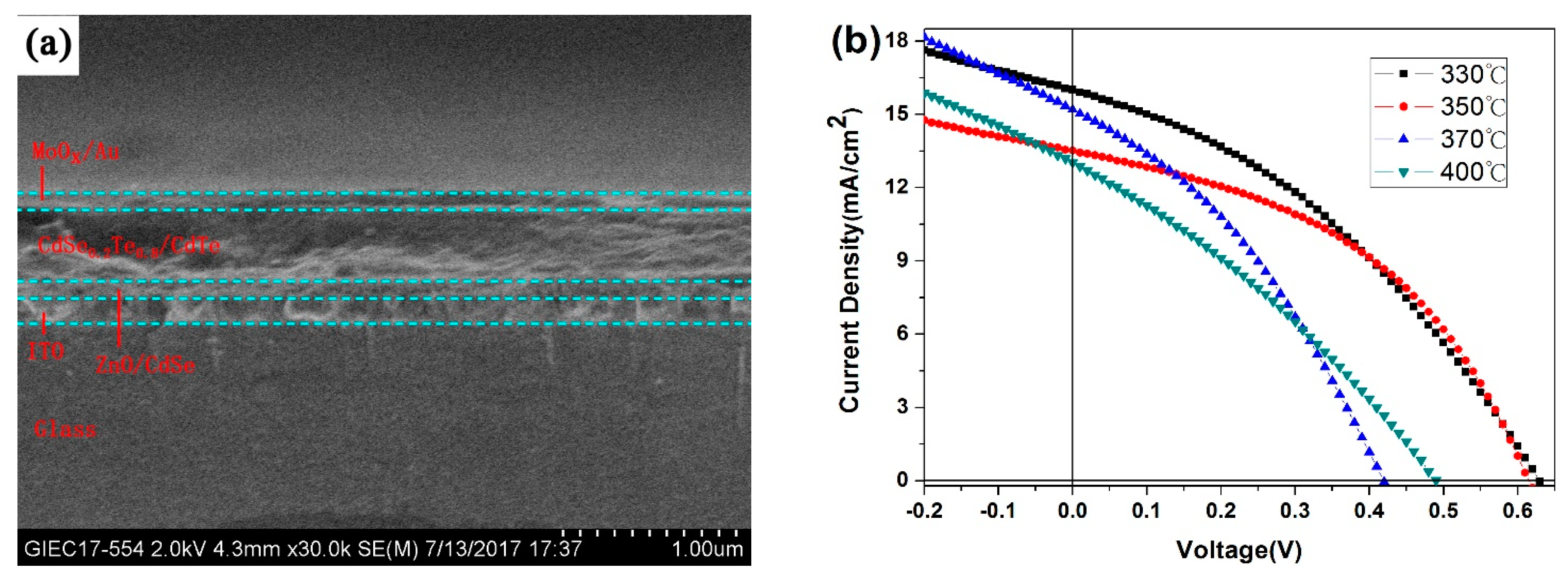
| Annealing Temperature (°C) | Voc (V) | Jsc (mA/cm2) | FF (%) | PCE (%) |
|---|---|---|---|---|
| 330 | 0.62 | 13.55 | 43.67 | 3.67 |
| 350 | 0.63 | 16.04 | 36.68 | 3.71 |
| 370 | 0.42 | 15.23 | 35.22 | 2.25 |
| 400 | 0.49 | 13.06 | 31.11 | 1.99 |
| Device | Voc (V) | Jsc (mA/cm2) | FF (%) | PCE (%) | (Ω·cm2) | (Ω·cm2) |
|---|---|---|---|---|---|---|
| ITO/ZnO/CdSe/CdSe0.05Te0.95/CdTe/MoOx/Au | 0.69 | 11.31 | 32.77 | 2.56 | 28.32 | 227.97 |
| ITO/ZnO/CdSe/CdSe0.1 Te0.9/CdTe/MoOx/Au | 0.66 | 16.32 | 44.10 | 4.77 | 22.15 | 244.44 |
| ITO/ZnO/CdSe/CdSe0.2 Te0.8/CdTe/MoOx/Au | 0.63 | 16.54 | 54.93 | 5.75 | 9.24 | 442.68 |
| ITO/ZnO/CdSe/CdSe0.4 Te0.6/CdTe/MoOx/Au | 0.63 | 16.32 | 35.26 | 3.64 | 17.99 | 87.36 |
| ITO/ZnO/CdSe/CdSe0.6 Te0.4/CdTe/MoOx/Au | 0.67 | 12.34 | 42.28 | 3.51 | 33.89 | 166.83 |
| ITO/ZnO/CdSe/CdSe0.8 Te0.2/CdTe/MoOx/Au | 0.60 | 10.26 | 38.78 | 2.39 | 33.30 | 226.21 |
| ITO/ZnO/CdSe/CdTe/MoOx/Au | 0.61 | 19.05 | 46.91 | 5.45 | 16.20 | 236.09 |
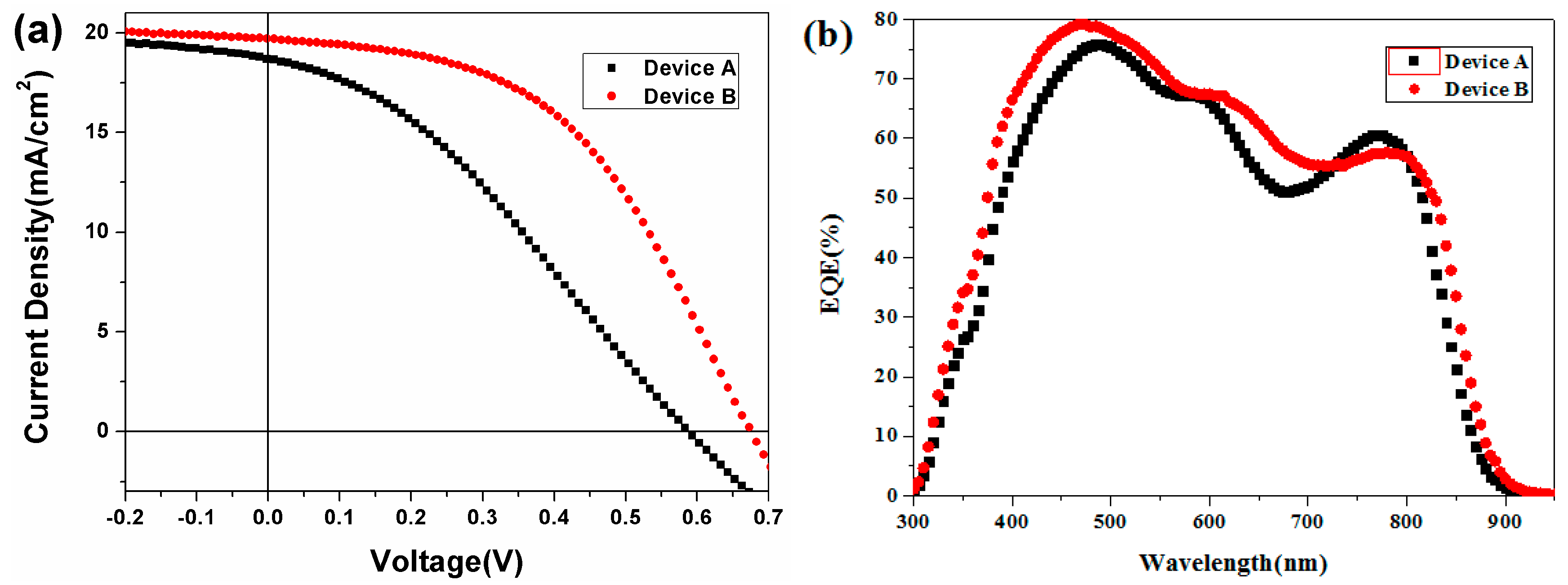
| Device | Voc (V) | Jsc (mA/cm2) | FF (%) | PCE (%) | (Ω·cm2) | (Ω·cm2) |
|---|---|---|---|---|---|---|
| ITO/ZnO/CdSe0.2Te0.8/CdTe/MoOx/Au | 0.59 | 18.59 | 32.56 | 4.03 | 25.94 | 147.68 |
| ITO/ZnO/CdSe0.8Te0.2/CdSe0.2Te0.8/CdTe/MoOx/Au | 0.67 | 19.70 | 48.25 | 6.37 | 15.00 | 422.13 |
© 2017 by the authors. Licensee MDPI, Basel, Switzerland. This article is an open access article distributed under the terms and conditions of the Creative Commons Attribution (CC BY) license (http://creativecommons.org/licenses/by/4.0/).
Share and Cite
Wen, S.; Li, M.; Yang, J.; Mei, X.; Wu, B.; Liu, X.; Heng, J.; Qin, D.; Hou, L.; Xu, W.; et al. Rationally Controlled Synthesis of CdSexTe1−x Alloy Nanocrystals and Their Application in Efficient Graded Bandgap Solar Cells. Nanomaterials 2017, 7, 380. https://doi.org/10.3390/nano7110380
Wen S, Li M, Yang J, Mei X, Wu B, Liu X, Heng J, Qin D, Hou L, Xu W, et al. Rationally Controlled Synthesis of CdSexTe1−x Alloy Nanocrystals and Their Application in Efficient Graded Bandgap Solar Cells. Nanomaterials. 2017; 7(11):380. https://doi.org/10.3390/nano7110380
Chicago/Turabian StyleWen, Shiya, Miaozi Li, Junyu Yang, Xianglin Mei, Bin Wu, Xiaolin Liu, Jingxuan Heng, Donghuan Qin, Lintao Hou, Wei Xu, and et al. 2017. "Rationally Controlled Synthesis of CdSexTe1−x Alloy Nanocrystals and Their Application in Efficient Graded Bandgap Solar Cells" Nanomaterials 7, no. 11: 380. https://doi.org/10.3390/nano7110380