Article

Investigation of the Band Structure of Graphene-Based Plasmonic Photonic Crystals

1
College of Information Science and Engineering, Huaqiao University, No. 668, Jimei Avenue, Jimei District, Xiamen 361021, China
2
Institute of Semiconductors, Chinese Academy of Sciences, 35A, Qinghua East Road, Haidian District, Beijing 100086, China
*
Author to whom correspondence should be addressed.
Nanomaterials 2016, 6(9), 166; https://doi.org/10.3390/nano6090166
Submission received: 23 July 2016 / Revised: 24 August 2016 / Accepted: 5 September 2016 / Published: 9 September 2016
(This article belongs to the Special Issue 2D Nanomaterials: Graphene and Beyond Graphene)

Abstract

:
In this paper, one-dimensional (1D) and two-dimensional (2D) graphene-based plasmonic photonic crystals (PhCs) are proposed. The band structures and density of states (DOS) have been numerically investigated. Photonic band gaps (PBGs) are found in both 1D and 2D PhCs. Meanwhile, graphene-based plasmonic PhC nanocavity with resonant frequency around 175 THz, is realized by introducing point defect, where the chemical potential is from 0.085 to 0.25 eV, in a 2D PhC. Also, the bending wvaguide and the beam splitter are realized by introducing the line defect into the 2D PhC.

1. Introduction

Photonic crystals (PhCs), first proposed by Yablonovitch [1] and John [2], have attracted great attention due to their unique properties, such as the self-collimation which can be applied to confine and guide light in photonic integrated circuits [3], the negative refraction which can be employed to focus light on a scale less than the square of light wavelength [4]. Furthermore, similar to the energy band gaps resulting from the electrons in a periodic potential, the photonic band gaps (PBGs) can also be obtained in medium with spatially periodical dielectric constant [5,6,7,8]. Light with a frequency within the PBGs is not allowed to propagate along the PhCs. However, conventional dielectric based PhC devices [9,10,11,12], usually in micrometer scale, are challenging to obtain a further size reduction due to the optical diffraction limit. Nevertheless, surface plasmon polaritons (SPPs), the electromagnetic waves propagating along an interface between a metal and a dielectric, enable the confinement of electromagnetic field to scales far below the optical diffraction limit [13]. This makes SPPs-based components significantly smaller than the wavelength [14]. However, noble plasmonic materials including gold and silver, are barely tunable and display enormous ohmic losses due to the evanescent characteristic of SPPs, which greatly limit their applications in nano-optical devices.
Graphene, a two-dimensional (2D) carbon atomic crystal arranged in a honeycomb lattice [15], has demonstrated exceptional properties in electronics and photonics [16,17,18], involving a number of applications such as field-effect transistors [19,20,21], photodetectors [22,23] and high-speed optical modulators [24,25], etc. Unlike the conventional plasmonics based on noble metals, graphene supported SPPs have demonstrated extremely high confinement, highly tunability via electrical gating and chemical doping [26,27,28], and relatively low loss resulting from long plasmon lifetime [29,30]. These extraordinary properties make graphene a promising candidate for plasmonic material with broad applications from terahertz to mid-infrared span [31,32,33,34].
One of the typical structures of graphene-based one-dimensional (1D) plasmonic PhCs is graphene micro-ribbon arrays. Early in 2011, Ju et al. reported the tunability of plasmon excitations and light-plasmon coupling at terahertz in graphene micro-ribbon arrays [35]. Then, Nikitin et al. investigated the transmission, absorption and reflection properties of graphene micro-ribbon arrays [36]. Bludov et al. demonstrated that polaritonic crystal can be realized with monolayer graphene periodically modulated by gate electrode [37]. Furthermore, Yan et al. studied the magnetoplasmons of graphene disk arrays of micrometer [38], where they found that the plasmon lifetime in graphene can be continuously tuned via magnetic field, and the tunability of mode splitting. In the same year, Thongrattanasiri et al. demonstrated the complete optical absorption property with similar structure [39]. Other properties of interest including transparency and band structure are investigated using graphene/insulator stacks [40,41]. However, all of the above mentioned research concerned the interaction between the graphene periodical nano structures and the normal incident light. In other words, the reported work did not analyze the density of states (DOS) properties of the plasmonic crystals, which are significant important in the performance of the future plasmonic emitters. Further, in plane propagation properties of plasmons along the 2D graphene plasmonic crystal have never been reported.
In this paper, we proposed graphene-based plasmonic PhCs with ultra-small size. Both the band structure and the DOS of 1D and 2D PhCs are numerically studied by using the finite element method (FEM) with Comsol Multiphysics Radio Frequency (RF) Module, version 4.3b, commercial software. Further, 2D PhC nanocavity was obtained by introducing point defect, where the optical field was well-confined in the defect via tuning the chemical potential of graphene in the defective region. Also, the bending wvaguide and the beam splitter are realized by introducing the line defect into 2D PhC. These results provide new insight into the designing of PhC devices, including PhC waveguides, PhC nanocavities, plasmonic filter, plasmonic switch, etc.

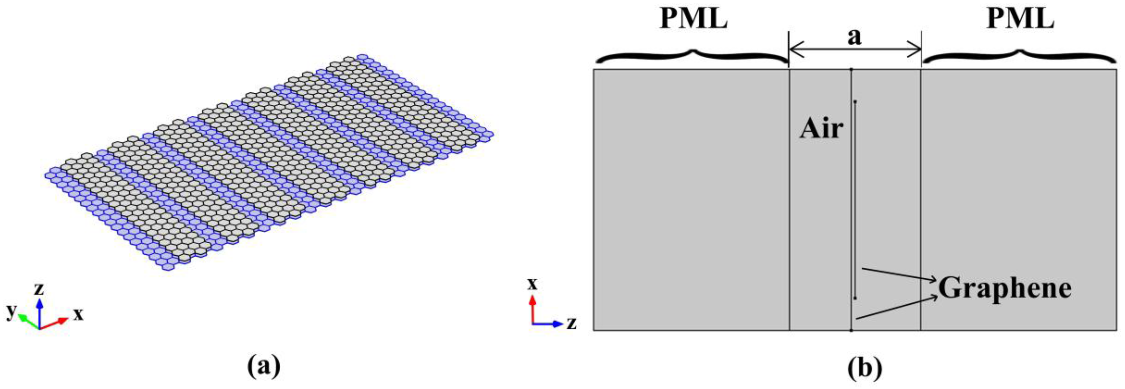
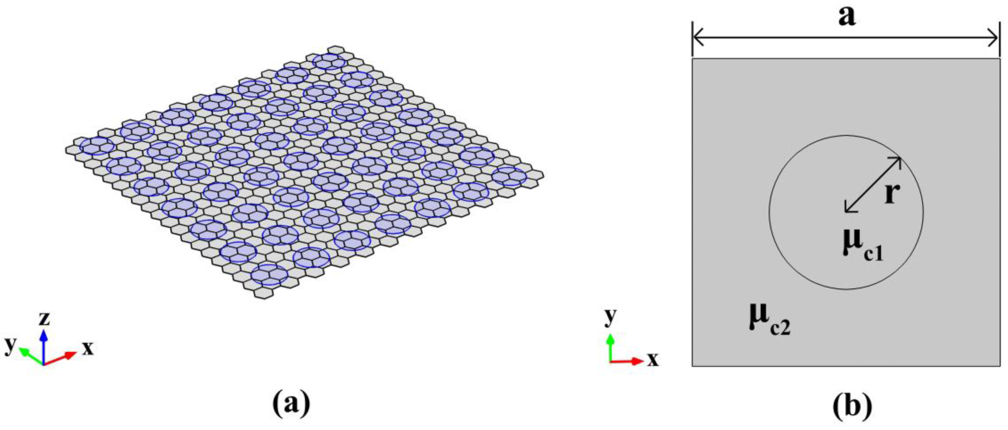
2. Simulation Methods and Models

To investigate 1D graphene-based plasmonic PhC, double-layer graphene, constituted by two graphene sheets with an interval of 0.3 nm, is periodically arranged along x direction to form the 1D PhC in our model. Figure 1a displays a three-dimensional (3D) view of a schematic diagram of the 1D PhC. In Figure 1b, we use two line segments to represent the cross section of double-layer graphene with the same chemical potential of 0.9 eV. The bottom layer with width of 20 nm, which plays the role of guiding SPPs, is continuously arranged. Periodically discrete graphene nanoribbons with a width of 15 nm, which can be used to tune the plasmons in the bottom layer, are employed to form the top layer.
The graphene sheet is treated as an ultra-thin film that can be characterized by surface conductivity in our model. Therefore, the surface current density of graphene is defined as J = σgE along the graphene sheet [42,43,44], where E is the electric field of the plasmon. The surface conductivity of graphene σg, constituted by the interband electron transitions σinter and the intraband electron-photon scattering σintra, is obtained from the Kubo formula [45,46,47,48],
σ g = σ int r a + σ int e r
with
σ int r a = i e 2 k B T π h 2 ( ω i / τ ) [ μ c k B T + 2 ln ( 1 + exp ( μ c k B T ) ) ]
σ int e r = i e 2 2 h ln [ 2   | μ c |     h   ( ω i / τ ) 2   | μ c |   +   h   ( ω i / τ ) ]
where μc is the chemical potential, kB is the Boltzmann constant, T is the temperature, ω is the angular frequency of the plasmon, and τ is the electron momentum relaxation time. In this paper, we set T = 300 K, τ = 0.5 ps.
As for 2D plasmonic PhC, we use monolayer graphene with periodically modified chemical potential, to form the 2D plasmonic PhC with square lattice and lattice constant a = 20 nm. Figure 2a displays the 3D view of schematic diagram of 2D PhC, and as shown in Figure 2b, a circle with chemical potential μc1, is surrounded by the same sheet of graphene with a different chemical potential μc2. The graphene material can be characterized by effective index defined as neff = 𝛽/k0, where k0 is the wave number in free space. As for transverse magnetic (TM) mode, the propagation constants of SPPs supported by a single-layer graphene, can be expressed as [49,50,51,52]
β = k 0 1 ( 2 η 0 σ g ) 2
where η0 (377 Ω) is the intrinsic impedance of the free space. As far as band structure calculations are concerned, it is generally sufficient to consider the wave vector k around the edge of the irreducible Brillouin zone (IBZ: form Г to X to M) while ignoring the inner region, which can be justified from the symmetry of the structure.
Similar to the electronic density of states which experience significant modifications in a semiconductor, the periodic modulation of the dielectric constant results in a photonic DOS. Photonic DOS is defined as the number of the PhC Eigen-state inside the unit frequency range. The DOS is calculated by counting all allowed states within the frequency region of an infinitesimally small interval, which is expressed as follows [53,54]:
N ( ω ) = n B Z d 2 k δ ( ω ω n ( k ) )
here the multiplication by the delta-function δ ( ω ω n ( k ) ) corresponds to making the extract of the Eigen-states with the same frequency. After the extraction, the integration is carried out. This means summation of the Eigen-states with the same frequencies within one band. After integration, the summation over all the bands is obtained.

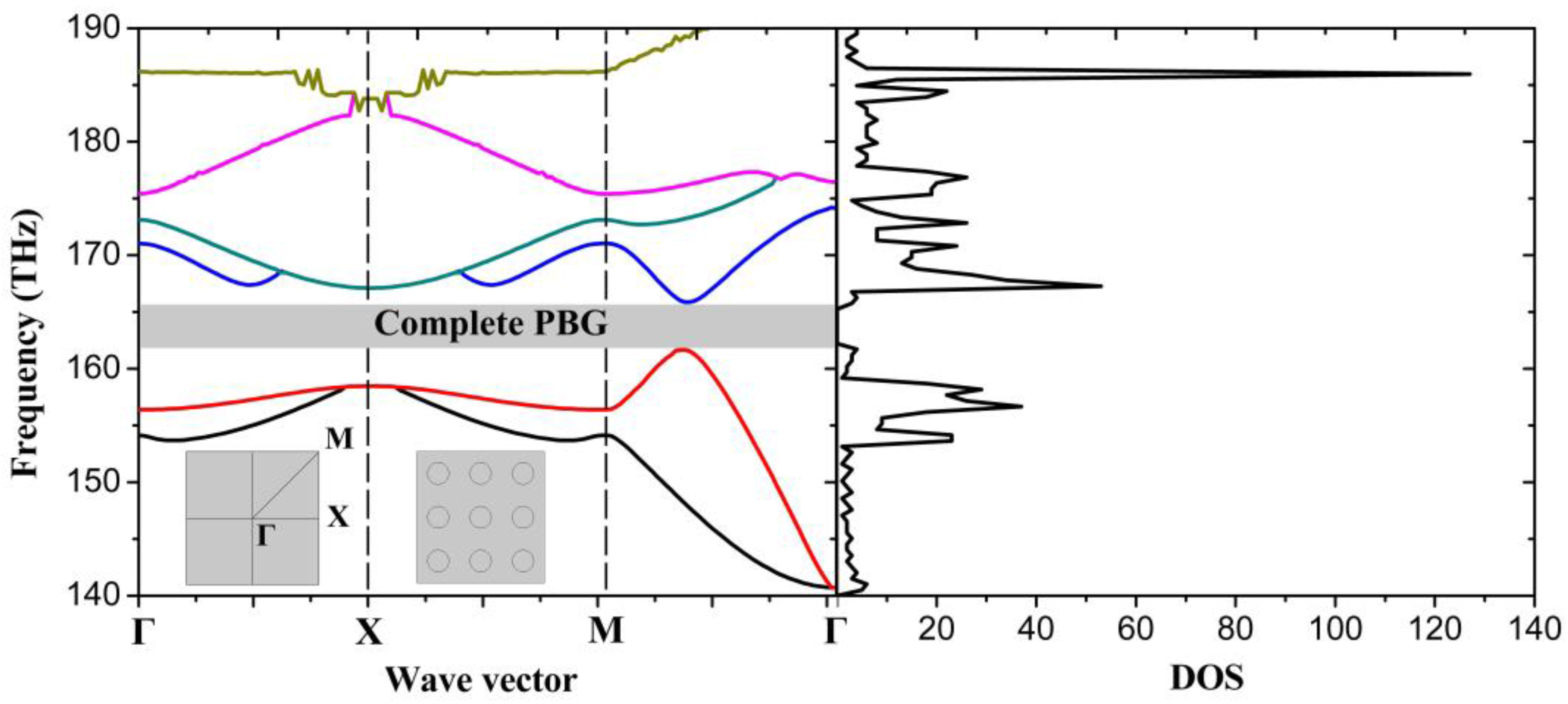
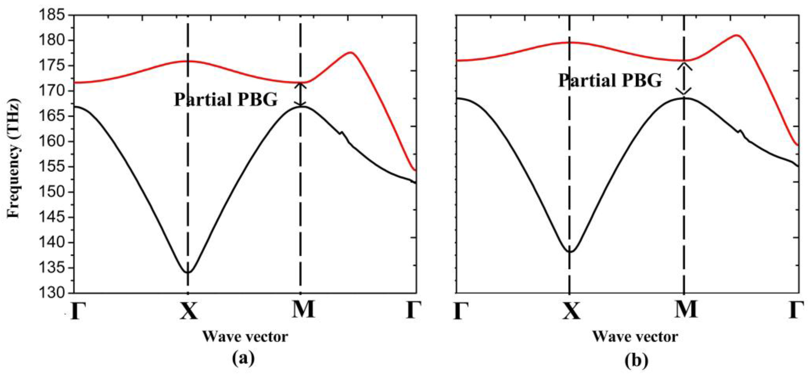
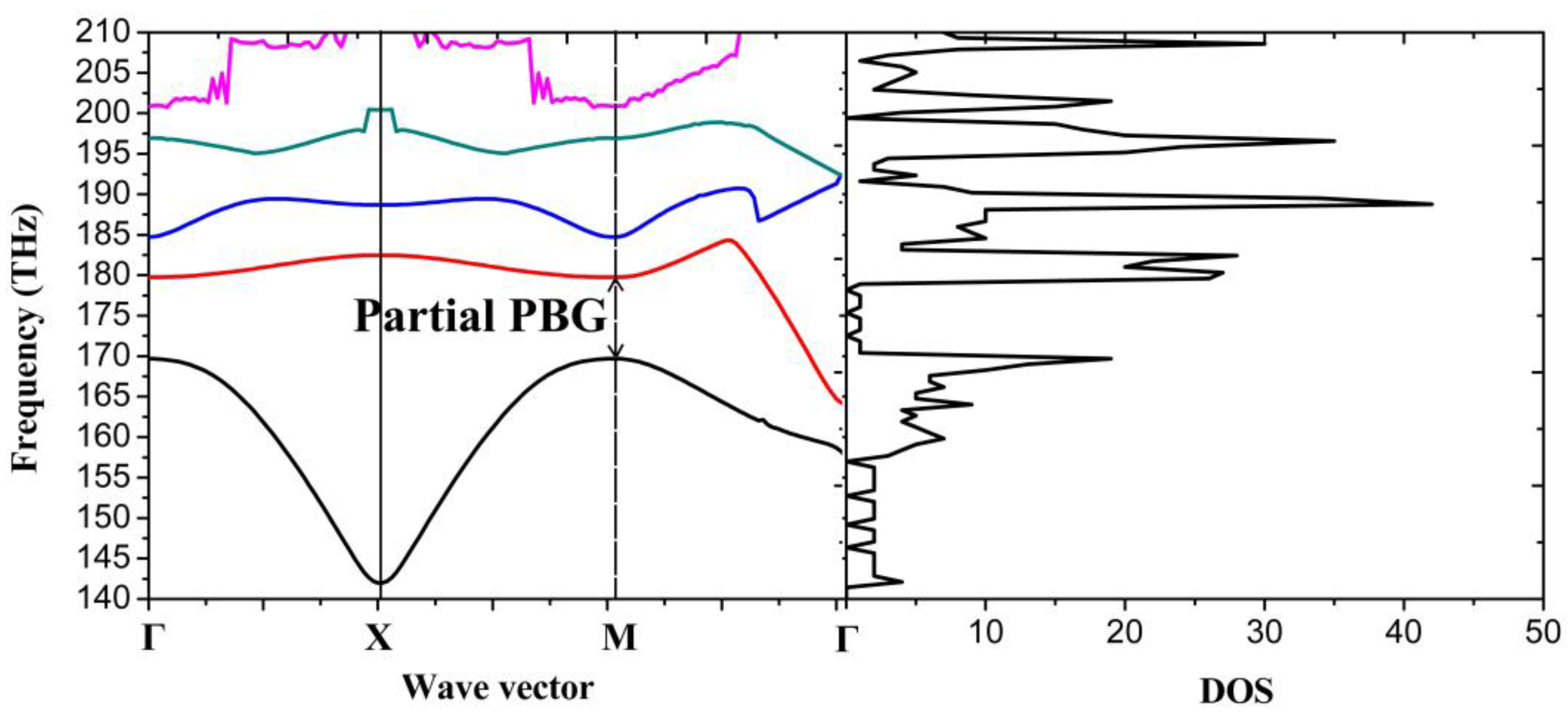
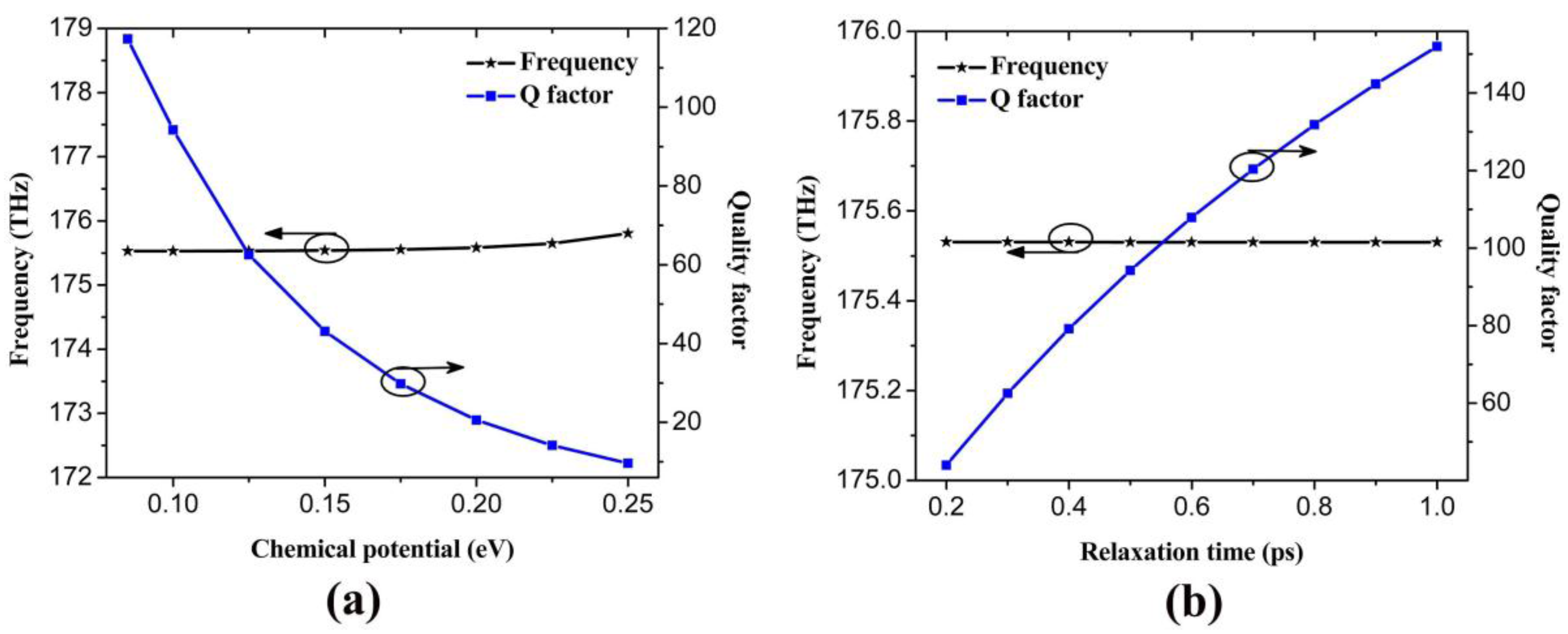
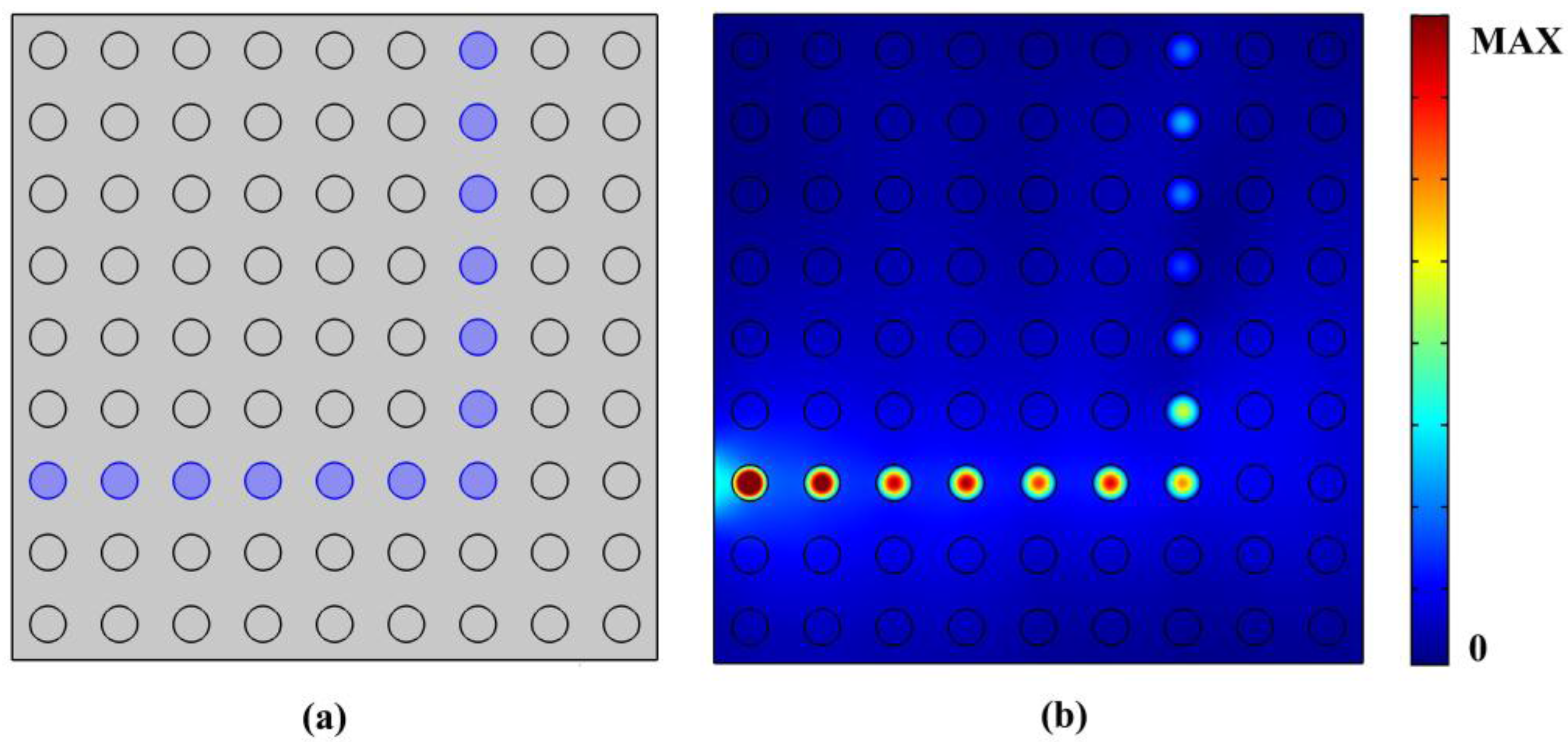
3. Results and Discussion

The periodicity of PhCs results in PBGs where no electromagnetic modes are allowed to have frequencies in the gaps. To obtain the band structure of plasmonic PhC, we need to iterate Eigen-frequency in each k point precisely due to the frequency dependent dielectric constant which results in the analytical solutions hardly being acquired. Figure 3 displays the band structure of 1D plasmonic PhC, and the corresponding DOS, with frequency from 120 THz to 255 THz. There are several PBGs from 142.9 THz to 149.9 THz, 170.2 THz to 177.1 THz, 181.5 THz to 192.9 THz and so on, where there are almost zero photonic DOS which correspond to the absence of the Eigen-states within corresponding frequency range.
Furthermore, we modify the width of graphene nanoribbon in the top layer to see how the band structure changes. Figure 4a,b show the first two bands corresponding to the graphene nanoribbon with width of 13 nm and 17 nm respectively. The two bands cover the frequency range from 135.5 THz to 150.4 THz and 166.4 THz to 175.9 THz when we set the width of graphene nanoribbon as 13 nm, which displays a large PBG of 16 THz. However, when we increase the width of nanoribbon to 17 nm, the PBG can only cover frequency range from 163.5 THz to 164.6 THz. It can be seen that both the band position and bandwidth can be effectively tuned via modifying the width of graphene nanoribbon.
In the same way as for 1D plasmonic PhCs, the band structure of 2D plasmonic PhCs can be calculated for a square lattice of 2D PhC with modified chemical potential. Figure 5 displays the band structure of graphene-based 2D plasmonic PhC with μc1 = 0.9 eV, μc2 = 0.6 eV, and the corresponding DOS. At some specific frequencies, the band gaps are overlapped forming so-called complete PBG with frequency range from 161.7 THz to 165.9 THz, which means that plasmons will not propagate inside the PhC at any angle. Moreover, the DOS within PBG is almost zero, which means there is no allowed Eigen-state in this frequency range.
As it can be seen from Figure 6 with μc1 = 0.6 eV, μc2 = 0.9 eV, within all the investigated frequency ranges at least one Eigen-state exists, so no complete PBG appears. The first band covers the frequency range from 142.0 THz to 169.7 THz, the second band covers the frequency range from 164.1 THz to 184.3 THz, etc. However, considering the band structure, it is demonstrated that the PhC has wide partial PBGs at some certain propagation directions. For example, there are no Eigen-frequencies at the point M within the frequency range from 169.7 THz to 179.7 THz, which means that the light with frequency in this range propagating in the corresponding direction is forbidden.
In order to tune the partial PBG (shown in Figure 6), we modify the chemical potential of the circle. As it can be seen from Figure 7a,b, the partial PBGs cover the frequency range from 166.9 THz to 171.6 THz and 168.5 THz to 176 THz, when we set μc2 as 0.8 eV and 0.85 eV, respectively. Both the band position and bandwidth can be tuned distinguishedly.

4. Applications of Graphene Based Plasmonic Photonic Crystals (PhCs)

As an application of graphene based plasmonic PhC proposed in this paper, the properties of the nanocavity formed by the point defect. To obtain PhC nanocavity, we introduce point defect into 3 × 3 PhCs, i.e., modifying the chemical potential of the central circle in Figure 8a. Figure 8a displays the schematic of the nanocavity with μc1 = 0.6 eV, μc2 = 0.9 eV, and the chemical potential of the defect is μc3. As it can be seen from Figure 8b, the PhC nanocavity, with a light field well-confined within the defect region, can be realized.
Figure 9a plots the resonant frequency and quality (Q) factor for the resonant modes with the defect chemical potential μc3 from 0.085 eV to 0.25 eV. It can be seen that the resonant frequencies are around 175 THz where the partial PBG exists (shown in Figure 5), which means that we have successfully introduced a point defect into the earlier proposed plasmonic 2D PhC, resulting in the PhC nanocavity. However, with the increasing of chemical potential of the point defect, the Q factor of the nanocavity decreases from 117 to 9.6. For a given frequency, the momemtum of the plasmon supported by graphene is dependent on the chemical potential. In the proposed nanocavity, when chemical potential increases, it becomes close to the chemical potential outside the cavities, so the momentum became more matched to the enviroment. The plasmon turns to escape from the cavities resulting from the increasing radiation loss. Eventually, the Q factor dicreases. Figure 9b displays the resonant frequency and Q factor versus the relaxation time. The resonant frequency remains around 175 THz, but Q factor increases from 44 to 152 with the increasing relaxation time from 0.2 to 1 ps. This can be attributed to the reduction of the Ohmic absorption of the plasmons when the relaxation time of electron momentum increases. Note that the typical mode area of the nanocavities is in the order of 10−50)20 is the free space wavelength), which is comparable to the counterpart of the graphene coated InGaAs nanowire, and much smaller than the conventional cavities [31]. This nanocavity might be a fundermental component in the future high density integrated plasmonic circuit technique.
Practically, the means of fabrication of the proposed nano-cavity can follow the method proposed in Reference [34], where the graphene monolayer sits on a SiO2 on Si substrate. The thickness of the SiO2 layer is periodically modified to get the chemical potential of the graphene periodical variation when external electric field is applied. So the plasmonic crystal structure is achieved. When the thickness of one site of SiO2 is different from the regular value, the different chemical potential is obtained, and finally the nano-cavity is formed.
Another application of the 2D PhC is the beam splitter and bending waveguide. We introduce a line defect into 9 × 9 PhC. Figure 10a displays the schematic of the beam splitter with μc1 = 0.6 eV, μc2 = 0.9 eV. The path full of blue circles with chemical potential μc3 of 0.3 eV represents the line defects which we used to realize the PhC beam splitter. Figure 10b shows the normalized magnetic distribution of the beam splitter with operation frequency of 9.8e13 Hz, where it can be seen that light was exactly transmitted through the routes we designed, and can also be well-confined within the defective region.
Figure 11a shows a bending waveguide with a line defect in the same crystal structure in Figure 10. The path full of blue circles with chemical potential μc3 of 0.3 eV represents the line defects. Figure 11b displays the normalized magnetic distribution of the bending waveguide with a frequency of 9.8e13 Hz, where it can be seen that a 90 degree bending of waveguide with high confinement is realized by the proposed structure.

5. Conclusions

In summary, graphene-based 1D and 2D plasmonic PhCs are proposed, where the band structure and the DOS are numerically investigated. Several PBGs of 1D PhC are found, and there is no Eigen-state within the frequency range where PBGs exist. Meanwhile, we have found complete PBGs with frequency range from 161.7 THz to 165.9 THz for 2D PhC with μc1 = 0.9 eV, μc2 = 0.6 eV, and partial PBGs with frequency range from 169.7 THz to 179.7 THz for 2D PhC with μc1 = 0.6 eV, μc2 = 0.9 eV. The PhC nanocavity with resonant frequency around 175 THz was realized by introducing point defect into the 3 × 3 PhCs with an ultra-small size of 60 × 60 nm. Also, the bending wvaguide and the beam splitter are proposed by introducing the line defect in the crystal structure. The proposed graphene based PhC structure might find broad applications in the future high density plasmonic integrated circuit technique.

Acknowledgments

The authors are grateful to the support by the Natural Science Fund of China under grant No. 61378058, the Science and Technology Fund of Quanzhou under grant No. Z1424009, Fujian Province Science Funds for Distinguished Young Scholar (No. 2015J06015) and the Promotion Program for Young and Middle-Aged Teachers in Science and Technology Research of Huaqiao University (No. ZQN-YX203).

Author Contributions

Weibin Qiu provided the original idea; Pingping Qiu and Houbo Chen designed the models; Pingping Qiu and Yixin Tang performed the simulations; Pingping Qiu, Zhili Lin, Jia-Xian Wang, Qiang Kan and Jiao-Qing Pan analyzed the data; Pingping Qiu and Weibin Qiu wrote the paper.

Conflicts of Interest

The authors declare no conflict of interest.

References

  1. Yablonovitch, E. Inhibited Spontaneous Emission in Solid-State Physics and Electronics. Phys. Rev. Lett. 1987, 58, 841–844. [Google Scholar] [CrossRef] [PubMed]
  2. John, S. Strong Localization of Photons in Certain Disordered Dielectric Superlattices. Phys. Rev. Lett. 1987, 58, 2486–2489. [Google Scholar] [CrossRef] [PubMed]
  3. Prather, D.W.; Shi, S.; Murakowski, J. Self-collimation in photonic crystal structures: A new paradigm for applications and device development. Appl. Phys. 2007, 40, 2635–2651. [Google Scholar] [CrossRef]
  4. Dong, G.Y.; Yang, X.L.; Cai, L.Z. Anomalous refractive effects in honeycomb lattice photonic crystals formed by holographic lithography. Opt. Express 2010, 18, 16302–16308. [Google Scholar] [CrossRef] [PubMed]
  5. Knight, J.C.; Broeng, J.; Birks, T.A. Photonic Band Gap Guidance in Optical Fibers. Science 1998, 282, 1476–1478. [Google Scholar] [CrossRef] [PubMed]
  6. Cregan, R.F.; Mangan, B.J.; Knight, J.C.; Birks, T.A.; Russell, P.S.; Roberts, P.J.; Allan, D.C. Single-Mode Photonic Band Gap Guidance of Light in Air. Science 1999, 285, 1537–1539. [Google Scholar] [CrossRef] [PubMed]
  7. Yablonovitch, E.; Gmitter, T.J.; Leung, K.M. Photonic Band Structure: The Face-Centered-Cubic Case Employing Nonspherical Atoms. Phys. Rev. Lett. 1991, 67, 2295–2298. [Google Scholar] [CrossRef] [PubMed]
  8. Yablonovitch, E. Photonic band-gap structures. JOSA B 1993, 10, 283–295. [Google Scholar] [CrossRef]
  9. Kuramochi, E.; Nozaki, K.; Shinya, A.; Takeda, K.; Sato, T.; Matsuo, S.; Taniyama, H.; Sumikura, H.; Notomi, M. Large-scale integration of wavelength-addressable all-optical memories on a photonic crystal chip. Nat. Photon. 2014, 8, 474–481. [Google Scholar] [CrossRef]
  10. Yu, S.P.; Hood, J.D.; Muniz, J.A.; Martin, M.J.; Norte, R.; Hung, C.L.; Meenehan, S.M.; Cohen, J.D.; Painter, O.; Kimble, H.J. Nanowire photonic crystal waveguides for single-atom trapping and strong light-matter interactions. Appl. Phys. Lett. 2014, 104, 929–938. [Google Scholar] [CrossRef]
  11. Sciancalepore, C.; Bakir, B.B.; Letartre, X.; Harduin, J.; Olivier, N.; Seassal, C.; Fedeli, J.; Viktorovitch, P. CMOS-Compatible Ultra-Compact 1.55-µm Emitting VCSELs Using Double Photonic Crystal Mirrors. IEEE Photon. Technol. Lett. 2012, 24, 455–457. [Google Scholar] [CrossRef]
  12. Takeda, K.; Sato, T.; Shinya, A.; Nozaki, K.; Kobayashi, W.; Taniyama, H.; Notomi, M.; Hasebe, K.; Kakitsuka, T.; Matsuo, S. Few-fJ/bit data transmissions using directly modulated lambda-scale embedded active region photonic-crystal lasers. Nat. Photon. 2013, 7, 569–575. [Google Scholar] [CrossRef]
  13. Barnes, W.L.; Dereux, A.; Ebbesen, T.W. Surface plasmon subwavelength optics. Nature 2003, 424, 824–830. [Google Scholar] [CrossRef] [PubMed]
  14. Ditlbacher, H.; Krenn, J.R.; Schider, G.; Leitner, A.; Aussenegg, F.R. Two-dimensional optics with surface plasmon polaritons. Appl. Phys. Lett. 2002, 81, 1762–1764. [Google Scholar] [CrossRef]
  15. Novoselov, K.S.; Geim, A.K.; Morozov, S.V.; Jiang, D.; Katsnelson, M.I.; Grigorieva, I.V.; Dubonos, S.V.; Firsov, A.A. Two-dimensional gas of massless Dirac fermions in graphene. Nature 2005, 438, 197–200. [Google Scholar] [CrossRef] [PubMed] [Green Version]
  16. Avouris, P. Graphene: Electronic and Photonic Properties and Devices. Nano Lett. 2010, 10, 4285–4294. [Google Scholar] [CrossRef] [PubMed]
  17. Qiu, W.; Liu, X.; Zhao, J.; He, S.; Ma, Y.; Wang, J.; Pan, J. Nanofocusing of mid-infrared electromagnetic waves on graphene monolayer. Appl. Phys. Lett. 2014, 104. [Google Scholar] [CrossRef]
  18. Khaleque, A.; Hattori, H.T. Absorption enhancement in graphene photonic crystal structures. Appl. Opt. 2016, 55, 2936–2942. [Google Scholar] [CrossRef] [PubMed]
  19. Wang, L.; Meric, I.; Huang, P.Y.; Gao, Q.; Gao, Y.; Tran, H.; Taniguchi, T.; Watanabe, K.; Campos, L.M.; Muller, D.A.; et al. One-Dimensional Electrical Contact to a Two-Dimensional Material. Science 2013, 342, 614–617. [Google Scholar] [CrossRef] [PubMed]
  20. Li, X.; Wang, X.; Zhang, L.; Lee, S.; Dai, H. Chemically Derived, Ultrasmooth Graphene Nanoribbon Semiconductors. Science 2008, 319, 1229–1232. [Google Scholar] [CrossRef] [PubMed]
  21. Britnell, L.; Gorbachev, R.V.; Jalil, R.; Belle, B.D.; Schedin, F.; Mishchenko, A.; Georgiou, T.; Katsnelson, M.I.; Eaves, L.; Morozov, S.V.; et al. Field-effect tunneling transistor based on vertical graphene heterostructures. Science 2012, 335, 947–950. [Google Scholar] [CrossRef] [PubMed] [Green Version]
  22. Furchi, M.; Urich, A.; Pospischil, A.; Lilley, G.; Unterrainer, K.; Detz, H.; Klang, P.; Andrews, A.M.; Schrenk, W.; Strasser, G.; et al. Microcavity-Integrated Graphene Photodetector. Nano Lett. 2012, 12, 2773–2777. [Google Scholar] [CrossRef] [PubMed] [Green Version]
  23. Fang, Z.; Liu, Z.; Wang, Y.; Ajayan, P.M.; Nordlander, P.; Halas, N.J. Graphene-Antenna Sandwich Photodetector. Nano Lett. 2012, 12, 3808–3813. [Google Scholar] [CrossRef] [PubMed]
  24. Liu, M.; Yin, X.; Ulin-Avila, E.; Geng, B.; Zentgraf, T.; Ju, L.; Wang, F.; Zhang, X. A graphene-based broadband optical modulator. Nature 2011, 474, 64–67. [Google Scholar] [CrossRef] [PubMed]
  25. Lee, C.C.; Suzuki, S.; Xie, W.; Schibli, T.R. Broadband graphene electro-optic modulators with sub-wavelength thickness. Opt. Express 2012, 20, 5264–5269. [Google Scholar] [CrossRef] [PubMed]
  26. Chen, J.; Badioli, M.; Alonso-González, P.; Thongrattanasiri, S.; Huth, F.; Osmond, J.; Spasenović, M.; Centeno, A.; Pesquera, A.; Godignon, P.; et al. Optical nano-imaging of gate-tunable graphene plasmons. Nature 2012, 487, 77–81. [Google Scholar] [CrossRef] [PubMed]
  27. Fei, Z.; Rodin, A.S.; Andreev, G.O.; Bao, W.; McLeod, A.S.; Wagner, M.; Zhang, L.M.; Zhao, Z.; Thiemens, M.; Dominguez, G.; et al. Gate-tuning of graphene plasmons revealed by infrared nano-imaging. Nature 2012, 487, 82–85. [Google Scholar] [CrossRef] [PubMed]
  28. Nikitin, A.Y.; Guinea, F.; García-Vidal, F.J. Edge and waveguide THz surface plasmon modes in graphene micro-ribbons. Phys. Rev. B 2011, 84, 1401–1408. [Google Scholar] [CrossRef]
  29. Koppens, F.H.L.; Chang, D.E.; Garcia de Abajo, F.J. Graphene plasmonics: A platform for strong light-matter interaction. Nano Lett. 2011, 11, 3370–3377. [Google Scholar] [CrossRef] [PubMed]
  30. Vakil, A.; Engheta, N. Transformation Optics Using Graphene. Science 2011, 332, 1291–1294. [Google Scholar] [CrossRef] [PubMed]
  31. Zhao, J.; Liu, X.; Qiu, W.; Ma, Y.; Huang, Y.; Wang, J.; Qiang, K.; Pan, J. Surface-plasmon-polariton whispering-gallery mode analysis of the graphene monolayer coated InGaAs nanowire cavity. Opt. Express 2014, 22, 5754–5761. [Google Scholar] [CrossRef] [PubMed]
  32. Jablan, M.; Buljan, H.; Soljačić, M. Plasmonics in graphene at infrared frequencies. Phys. Rev. B 2009, 80. [Google Scholar] [CrossRef]
  33. Tamagnone, M.; Gomez-Diaz, J.S.; Mosig, J.R.; Perruisseau-Carrier, J. Reconfigurable THz plasmonic antenna concept using a graphene stack. Appl. Phys. Lett. 2012, 101. [Google Scholar] [CrossRef]
  34. Shi, B.; Cai, W.; Zhang, X.; Xiang, Y.; Zhan, Y.; Geng, J.; Ren, M.; Xu, J. Tunable band-stop filters for graphene plasmons based on periodically modulated graphene. Sci. Rep. 2016, 6. [Google Scholar] [CrossRef] [PubMed]
  35. Long, J.; Baisong, G.; Jason, H.; Caglar, G.; Michael, M.; Zhao, H.; Hans, A.B.; Liang, X.G.; Zettl, A.; Ron, S.Y.; et al. Graphene plasmonics for tunable terahertz metamaterials. Nat. Nanotechnol. 2011, 6, 630–634. [Google Scholar] [CrossRef]
  36. Nikitin, A.Y.; Guinea, F.; Garcia-Vidal, F.J.; Martin-Moreno, L. Surface plasmon enhanced absorption and suppressed transmission in periodic arrays of graphene ribbons. Phys. Rev. B 2012, 85. [Google Scholar] [CrossRef]
  37. Bludov, Y.V.; Peres, N.M.R.; Vasilevskiy, M.I. Graphene-based polaritonic crystal. Phys. Rev. B 2012, 85, 762–767. [Google Scholar] [CrossRef]
  38. Yan, H.; Li, Z.; Li, X.; Zhu, W.; Avouris, P.; Xia, F. Infrared spectroscopy of tunable Dirac terahertz magneto-plasmons in graphene. Nano Lett. 2012, 12, 3766–3771. [Google Scholar] [CrossRef] [PubMed]
  39. Thongrattanasiri, S.; Koppens, F.H.L.; Garcia de Abajo, F.J. Complete optical absorption in periodically patterned graphene. Phys. Rev. Lett. 2012, 108, 799–802. [Google Scholar] [CrossRef] [PubMed]
  40. Yan, H.; Li, X.; Chandra, B.; Tulevski, G.; Wu, Y.; Freitag, M.; Zhu, W.; Avouris, P.; Xia, F. Tunable infrared plasmonic devices using graphene/insulator stacks. Nat. Nanotechnol. 2012, 7, 330–334. [Google Scholar] [CrossRef] [PubMed]
  41. Berman, O.L.; Boyko, V.S.; Kezerashvili, R.Y.; Kolesnikov, A.A.; Lozovik, Y.E. Graphene-based photonic crystal. Phys. Lett. A 2010, 374, 4784–4786. [Google Scholar] [CrossRef]
  42. Zhao, J.; Qiu, W.; Huang, Y.; Wang, J.X.; Kan, Q.; Pan, J.Q. Investigation of plasmonic whispering-gallery mode characteristics for graphene. Opt. Lett. 2014, 39, 5527–5530. [Google Scholar] [CrossRef] [PubMed]
  43. Huang, Y.; Zhao, J.; Qiu, W.; Lin, S.; Chen, H.; Wang, J.; Kan, Q.; Pan, J. Investigation of the tunable plasmonic whispering gallery mode properties for graphene monolayer nanodisk cavities. Optik 2016, 127, 5591–5596. [Google Scholar] [CrossRef]
  44. Nayyeri, V.; Soleimani, M. Modeling graphene in the Finite-Difference Time-Domain method using a surface boundary condition. IEEE Trans. Antennas Propag. 2013, 61, 4176–4182. [Google Scholar] [CrossRef]
  45. Hanson, G.W. Dyadic Green’s Functions and Guided Surface Waves for a Surface Conductivity Model of Graphene. J. Appl. Phys. 2008, 103. [Google Scholar] [CrossRef]
  46. Mak, J.C.C.; Sarris, C.D. FDTD-compatible broadband surface impedance boundary conditions for graphene. Electromagn. Adv. Appl. (ICEAA) 2013, 740–743. [Google Scholar]
  47. Amanatiadis, S.A.; Kantartzis, N.V.; Tsiboukis, T.D. A loss-controllable absorbing boundary condition for surface plasmon polaritons propagating onto graphene. IEEE Trans. Magn. 2015, 51, 1–4. [Google Scholar] [CrossRef]
  48. Yu, X.; Sarris, C.D. A perfectly matched layer for subcell FDTD and applications to the modeling of graphene structures. IEEE Antennas Wireless Propag. Lett. 2012, 11, 1080–1083. [Google Scholar]
  49. Qiu, W.; Liu, X.; Zhao, J.; Huang, Y.; Chen, H.; Li, B.; Wang, J.; Kan, Q.; Pan, J. Ultrabroad Band Rainbow Capture and Releasing in Graded Chemical Potential Distributed Graphene Monolayer. Plasmonics 2015, 10, 1023–1028. [Google Scholar] [CrossRef]
  50. Salonikios, V.; Amanatiadis, S.; Kantartzis, N.; Yioultsis, T. Modal analysis of graphene microtubes utilizing a two-dimensional vectorial finite element method. Appl. Phys. A 2016, 122, 1–7. [Google Scholar] [CrossRef]
  51. Mock, A. Pad´e approximant spectral fit for FDTD simulation of graphene in the near infrared. Opti. Mater. Express 2012, 2, 771–781. [Google Scholar] [CrossRef]
  52. Bouzianas, G.D.; Kantartzis, N.; Tsiboukis, T.D. Plasmon mode excitation on graphene layers via obliquely-incident focused wideband pulses in rigorous time-domain algorithms. IEEE Trans. Magn. 2013, 49, 1773–1776. [Google Scholar] [CrossRef]
  53. Jean-Michel, L.; Henri, B.; Vincent, B. Photonic Crystals: Towards Nanoscale Photonic Devices, 2nd ed.; Springer-Verlag: Berlin/Heidelberg, Germany, 2008; pp. 59–77. [Google Scholar]
  54. Sukhoivanov, I.A.; Igor, V.G. Photonic Crystals: Physics and Practical Modeling, 1st ed.; Springer-Verlag: Berlin/Heidelberg, Germany, 2009; pp. 96–103. [Google Scholar]
Figure 1. (a) The schematic view of the one-dimensional (1D) graphene-based plasmonic photonic crystal (PhC), where the blue denotes the bottom sheet graphene, and the grey denotes the graphene nanoribbons which modifies the plasmon propagating along the bottom sheet; (b) The computational window of 1D graphene-based plasmonic PhC with lattice constant a = 10 nm; The perfectly matched layer (PML) with width of 15 nm, is set up here as a non-reflecting boundary condition.
Nanomaterials 06 00166 g001
Figure 2. (a) Three-dimensional (3D) view of the proposed two-dimensional (2D) graphene-based plasmonic PhC. (b) The computational window of schematic diagram of graphene-based 2D plasmonic PhC, where lattice constant a = 20 nm, and r = 5 nm.
Nanomaterials 06 00166 g002
Figure 3. Band structure (left) and density of states (DOS) (right) of graphene-based plasmonic 1D PhC with chemical potential of 0.9 eV, and lattice constant a = 10 nm.
Nanomaterials 06 00166 g003
Figure 4. The first two bands of 1D PhC: (a) graphene nanoribbon with width of 13 nm; (b) graphene nanoribbon with width of 17 nm.
Nanomaterials 06 00166 g004
Figure 5. Band structure (left) and DOS (right) of graphene-based plasmonic 2D PhC with lattice constant a = 20 nm. The left inset shows the Brillouin zone, with the irreducible zone from 𝛤 to X to M. The right inset shows a view of the periodically modified chemical potential with μc1 = 0.9 eV, μc2 = 0.6 eV, and circular radius r = 5 nm.
Nanomaterials 06 00166 g005
Figure 6. Band structure (left) and DOS (right) of graphene-based plasmonic 2D PhC with chemical potential μc1 = 0.6 eV, μc2 = 0.9 eV, circular radius r = 5 nm, and lattice constant a = 20 nm.
Nanomaterials 06 00166 g006
Figure 7. The first two bands of 2D PhC: (a) μc1 = 0.6 eV, μc2 = 0.8 eV; (b) μc1 = 0.6 eV, μc2 = 0.85 eV.
Nanomaterials 06 00166 g007
Figure 8. (a) Schematic of PhC nanocavity with ultra-small size of 60 × 60 nm, μc1 = 0.6 eV, μc2 = 0.9 eV; (b) The normalized electric field distribution of the resonant modes of the defect, with μc3 from 0.085 eV to 0.25 eV.
Nanomaterials 06 00166 g008
Figure 9. (a) Resonant frequency and Q factor as a function of chemical potential of the point defect in 2D PhC, where μc3 is from 0.085 eV to 0.25 eV with μc1 = 0.6 eV, μc2 = 0.9 eV; (b) Resonant frequency and Q factor as a function of relaxation time with μc1 = 0.6 eV, μc2 = 0.9 eV, μc3 = 0.1 eV.
Nanomaterials 06 00166 g009
Figure 10. (a) Schematic of PhC beam splitter; (b) Normalized magnetic distribution of the PhC beam splitter with μc1 = 0.6 eV, μc2 = 0.9 eV, μc3 = 0.3 eV, operation frequency of 9.8e13 Hz.
Nanomaterials 06 00166 g010
Figure 11. (a) Schematic of PhC bending waveguide; (b) Normalized magnetic distribution of the PhC bending waveguide with μc1 = 0.6 eV, μc2 = 0.9 eV, μc3 = 0.3 eV, operation frequency of 9.8e13 Hz.
Nanomaterials 06 00166 g011

