
Electrically Tunable Absorption Enhancement with Spectral and Polarization Selectivity through Graphene Plasmonic Light Trapping


Abstract
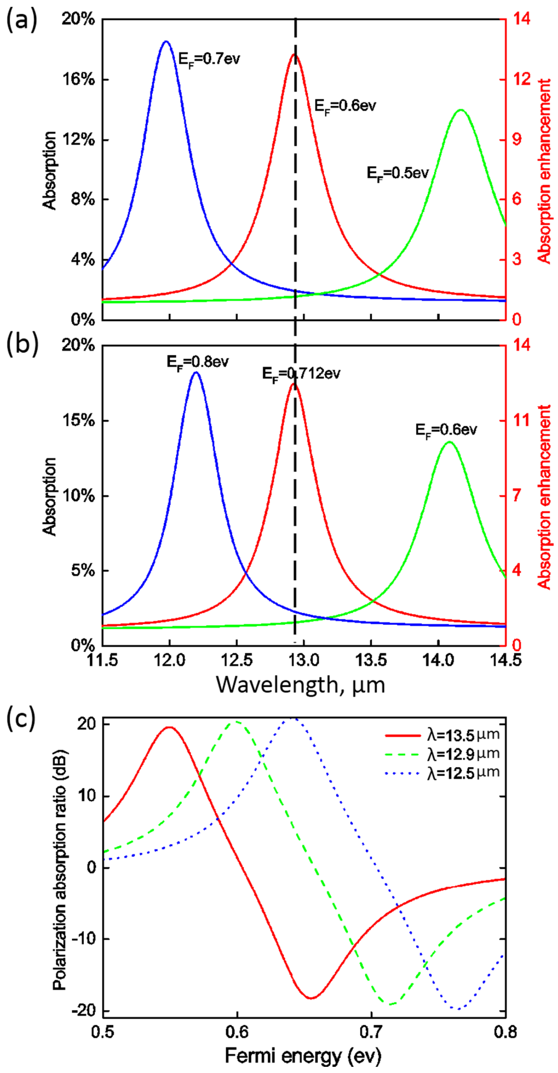
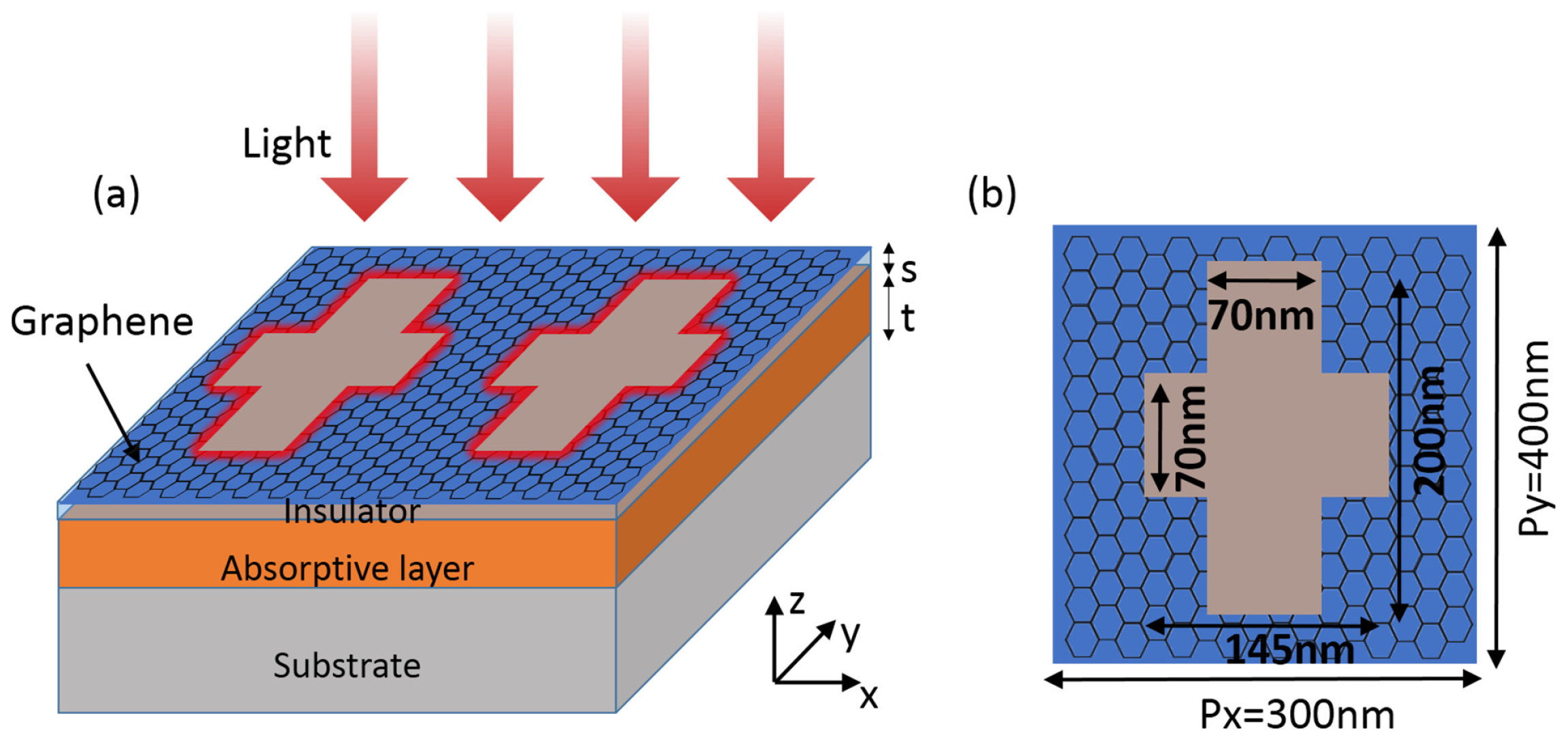
:
1. Introduction
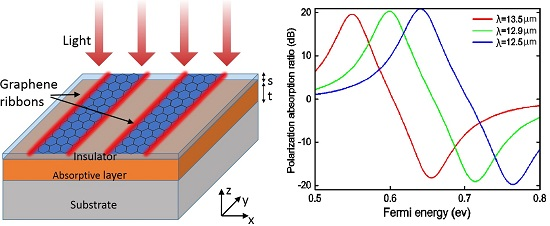
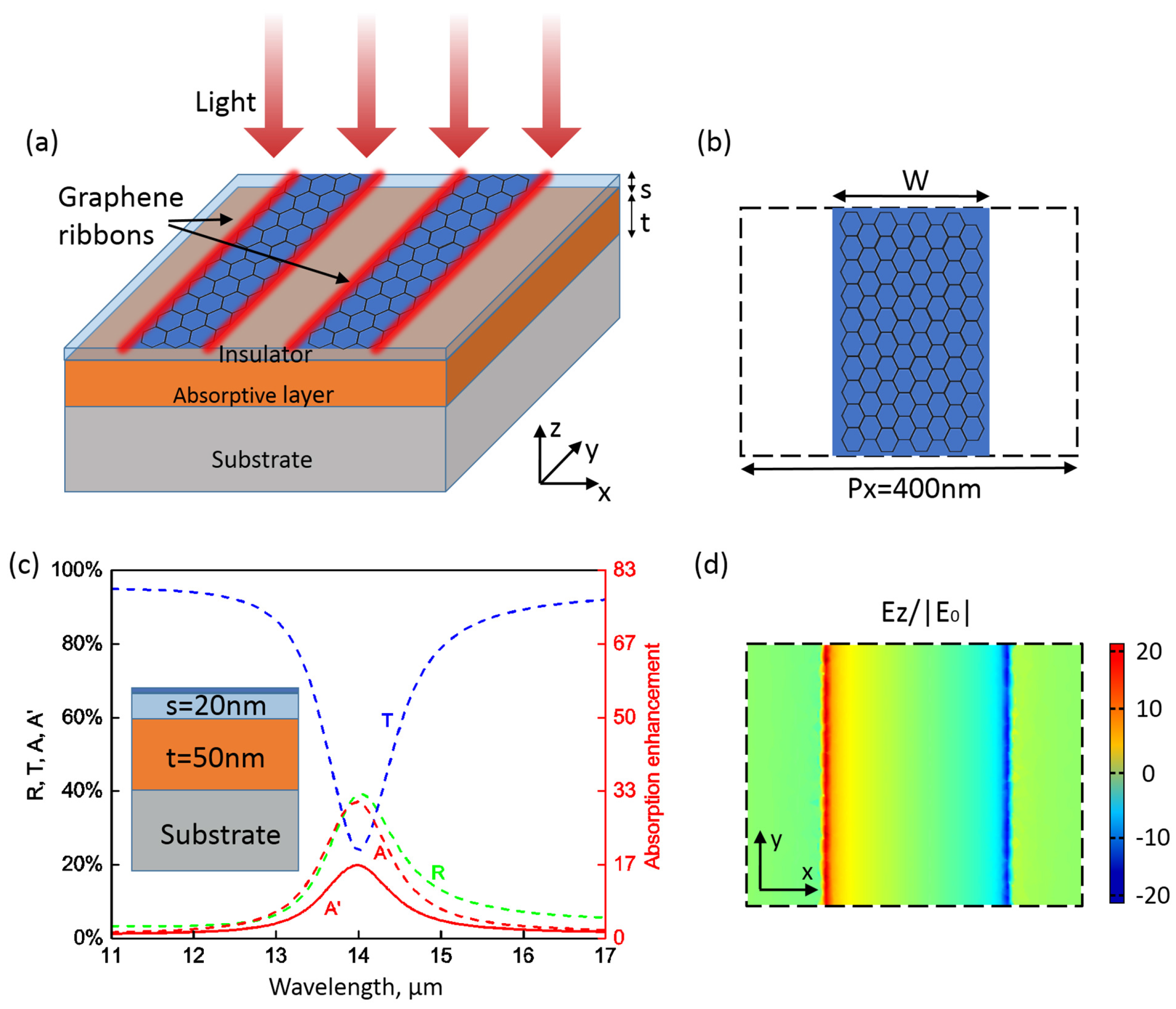
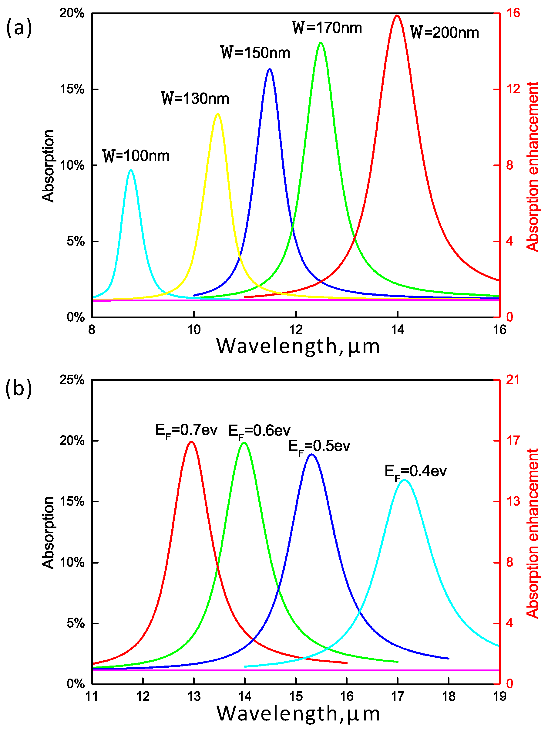
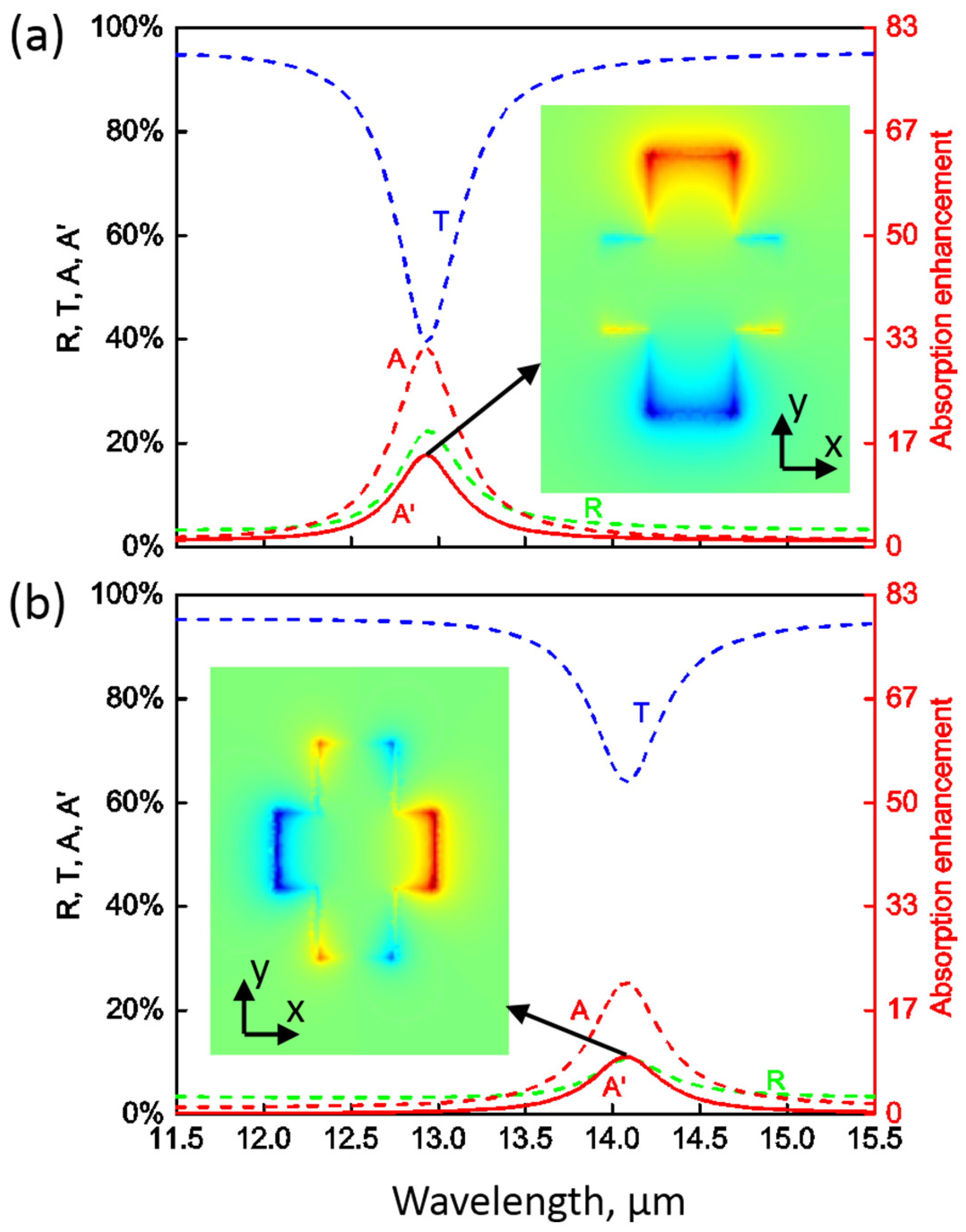
2. Results and Discussion
3. Conclusions
Acknowledgments
Author Contributions
Conflicts of Interest
References
- Atwater, H.A.; Polman, A. Plasmonics for improved photovoltaic devices. Nat. Mater. 2010, 9, 205–213. [Google Scholar] [CrossRef] [PubMed]
- Konstantatos, G.; Sargent, E.H. Nanostructured materials for photon detection. Nat. Nanotechnol. 2010, 5, 391–400. [Google Scholar] [CrossRef] [PubMed]
- Liu, Y.; Cheng, R.; Liao, L.; Zhou, H.; Bai, J.; Liu, G.; Liu, L.; Huang, Y.; Duan, X. Plasmon resonance enhanced multicolour photodetection by graphene. Nat. Commun. 2011, 2, 579. [Google Scholar] [CrossRef] [PubMed]
- Xu, T.; Wu, Y.K.; Luo, X.; Guo, L.J. Plasmonic nanoresonators for high-resolution colour filtering and spectral imaging. Nat. Commun. 2010, 1, 59. [Google Scholar] [CrossRef] [PubMed]
- Sobhani, A.; Knight, M.W.; Wang, Y.; Zheng, B.; King, N.S.; Brown, L.V.; Fang, Z.; Nordlander, P.; Halas, N.J. Narrowband photodetection in the near-infrared with a plasmon-induced hot electron device. Nat. Commun. 2013, 4, 1643. [Google Scholar] [CrossRef] [PubMed]
- Chen, J.; Badioli, M.; Alonso-González, P.; Thongrattanasiri, S.; Huth, F.; Osmond, J.; Spasenović, M.; Centeno, A.; Pesquera, A.; Godignon, P.; et al. Optical nano-imaging of gate-tunable graphene plasmons. Nature 2012, 487, 77–81. [Google Scholar] [CrossRef] [PubMed]
- Fei, Z.; Rodin, A.S.; Andreev, G.O.; Bao, W.; McLeod, A.S.; Wagner, M.; Zhang, L.M.; Zhao, Z.; Thiemens, M.; Dominguez, G.; et al. Gate-tuning of graphene plasmons revealed by infrared nano-imaging. Nature 2012, 487, 82–85. [Google Scholar] [CrossRef] [PubMed]
- Koppens, F.H.; Chang, D.E.; de Abajo, F.J.G. Graphene plasmonics: A platform for strong light–matter interactions. Nano Lett. 2011, 11, 3370–3377. [Google Scholar] [CrossRef] [PubMed]
- Zhang, J.; Guo, C.; Liu, K.; Zhu, Z.; Ye, W.; Yuan, X.; Qin, S. Coherent perfect absorption and transparency in a nanostructured graphene film. Opt. Express 2014, 22, 12524–12532. [Google Scholar] [CrossRef] [PubMed]
- Zhang, J.; Zhu, Z.; Liu, W.; Yuan, X.; Qin, S. Towards photodetection with high efficiency and tunable spectral selectivity: Graphene plasmonics for light trapping and absorption engineering. Nanoscale 2015, 7, 13530–13536. [Google Scholar] [CrossRef] [PubMed]
- Palik, E.D. Handbook of Optical Constants of Solids; Academic Press: Boston, MA, USA, 1998; Volume 3. [Google Scholar]
- Thongrattanasiri, S.; Koppens, F.H.; de Abajo, F.J.G. Complete optical absorption in periodically patterned graphene. Phys. Rev. Lett. 2012, 108, 047401. [Google Scholar] [CrossRef] [PubMed]
- Vakil, A.; Engheta, N. Transformation optics using graphene. Science 2011, 332, 1291–1294. [Google Scholar] [CrossRef] [PubMed]
- Yao, Y.; Kats, M.A.; Genevet, P.; Yu, N.; Song, Y.; Kong, J.; Capasso, F. Broad electrical tuning of graphene-loaded plasmonic antennas. Nano Lett. 2013, 13, 1257–1264. [Google Scholar] [CrossRef] [PubMed]
- Falkovsky, L.; Pershoguba, S. Optical far-infrared properties of a graphene monolayer and multilayer. Phys. Rev. B 2007, 76, 153410. [Google Scholar] [CrossRef]
- Falkovsky, L.; Varlamov, A. Space-time dispersion of graphene conductivity. Eur. Phys. J. B 2007, 56, 281–284. [Google Scholar] [CrossRef]
- Hanson, G.W. Quasi-transverse electromagnetic modes supported by a graphene parallel-plate waveguide. J. Appl. Phys. 2008, 104, 084314. [Google Scholar] [CrossRef]
- Jablan, M.; Buljan, H.; Soljačić, M. Plasmonics in graphene at infrared frequencies. Phys. Rev. B 2009, 80, 245435. [Google Scholar] [CrossRef]
- Fang, Z.; Thongrattanasiri, S.; Schlather, A.; Liu, Z.; Ma, L.; Wang, Y.; Ajayan, P.M.; Nordlander, P.; Halas, N.J.; de Abajo, F.J.G. Gated tunability and hybridization of localized plasmons in nanostructured graphene. ACS Nano 2013, 7, 2388–2395. [Google Scholar] [CrossRef] [PubMed]
- Grigorenko, A.; Polini, M.; Novoselov, K. Graphene plasmonics. Nat. Photonics 2012, 6, 749–758. [Google Scholar] [CrossRef]
- Zhu, Z.; Guo, C.; Liu, K.; Zhang, J.; Ye, W.; Yuan, X.; Qin, S. Electrically controlling the polarizing direction of a graphene polarizer. J. Appl. Phys. 2014, 116, 104304. [Google Scholar] [CrossRef]
- Zhu, Z.; Guo, C.; Liu, K.; Zhang, J.; Ye, W.; Yuan, X.; Qin, S. Electrically tunable polarizer based on anisotropic absorption of graphene ribbons. Appl. Phys. A 2014, 114, 1017–1021. [Google Scholar] [CrossRef]
- Ding, J.; Arigong, B.; Ren, H.; Shao, J.; Zhou, M.; Lin, Y.; Zhang, H. Mid-infrared tunable dual-frequency cross polarization converters using graphene-based L-shaped nanoslot array. Plasmonics 2015, 10, 351–356. [Google Scholar] [CrossRef]


© 2016 by the authors; licensee MDPI, Basel, Switzerland. This article is an open access article distributed under the terms and conditions of the Creative Commons Attribution (CC-BY) license (http://creativecommons.org/licenses/by/4.0/).
Share and Cite
Liu, W.; Zhang, J.; Zhu, Z.; Yuan, X.; Qin, S. Electrically Tunable Absorption Enhancement with Spectral and Polarization Selectivity through Graphene Plasmonic Light Trapping. Nanomaterials 2016, 6, 155. https://doi.org/10.3390/nano6090155
Liu W, Zhang J, Zhu Z, Yuan X, Qin S. Electrically Tunable Absorption Enhancement with Spectral and Polarization Selectivity through Graphene Plasmonic Light Trapping. Nanomaterials. 2016; 6(9):155. https://doi.org/10.3390/nano6090155
Chicago/Turabian StyleLiu, Wenbin, Jianfa Zhang, Zhihong Zhu, Xiaodong Yuan, and Shiqiao Qin. 2016. "Electrically Tunable Absorption Enhancement with Spectral and Polarization Selectivity through Graphene Plasmonic Light Trapping" Nanomaterials 6, no. 9: 155. https://doi.org/10.3390/nano6090155