Numerical Modeling of Sub-Wavelength Anti-Reflective Structures for Solar Module Applications

Abstract
:
1. Introduction
1.1. Scope
1.2. Background on Anti-Reflective Sub-Wavelength Structures

1.3. Ideal Anti-Reflective Sub-Wavelength Structures and Gradient Indexes
1.4. Properties of ARSWS Models

1.5. Commercial EM Modeling Software Packages
1.6. Utility of Modeling ARSWS
2. Overview of Optical Modeling Methods
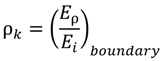
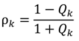
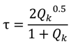
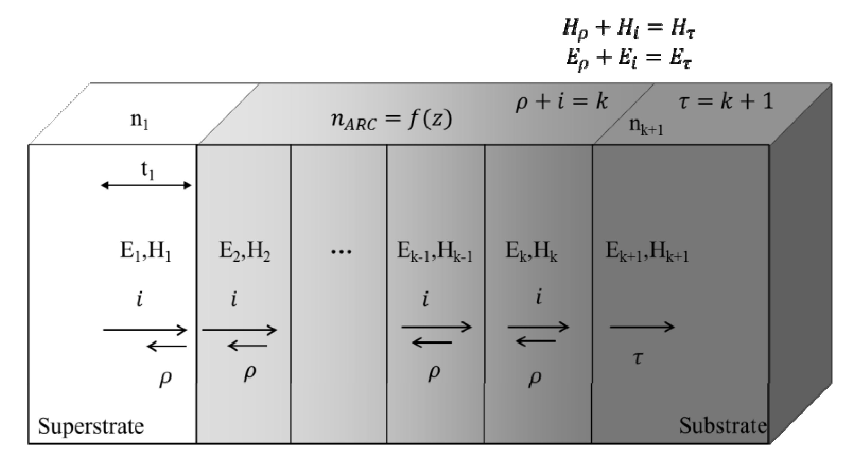
3. Effective Medium Theory

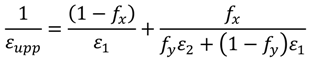

Effective Medium Approximations

| Method | Model | Notes |
|---|---|---|
| Maxwell-Garnett [16,18] |  | Original model for effective index of refraction (RI), assumes homogenous mixture of low volume fraction of spherical sub-wavelength structures (SWS) for material 2 |
| Bruggeman [19] |  | Describes effective RI for any number, k, of constituents in a homogeneous mixture |
| Lorentz-Lorentz [17] |  | Can be extended to more than two constituents by adding more terms |


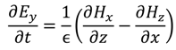
4. Time-Based Optical Modeling Methods
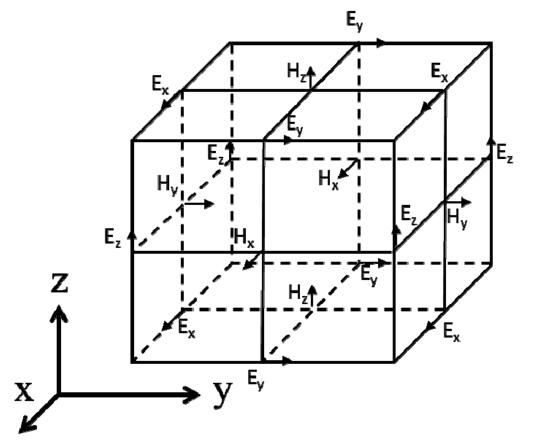
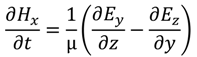
Finite-Difference Time-Domain
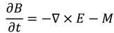

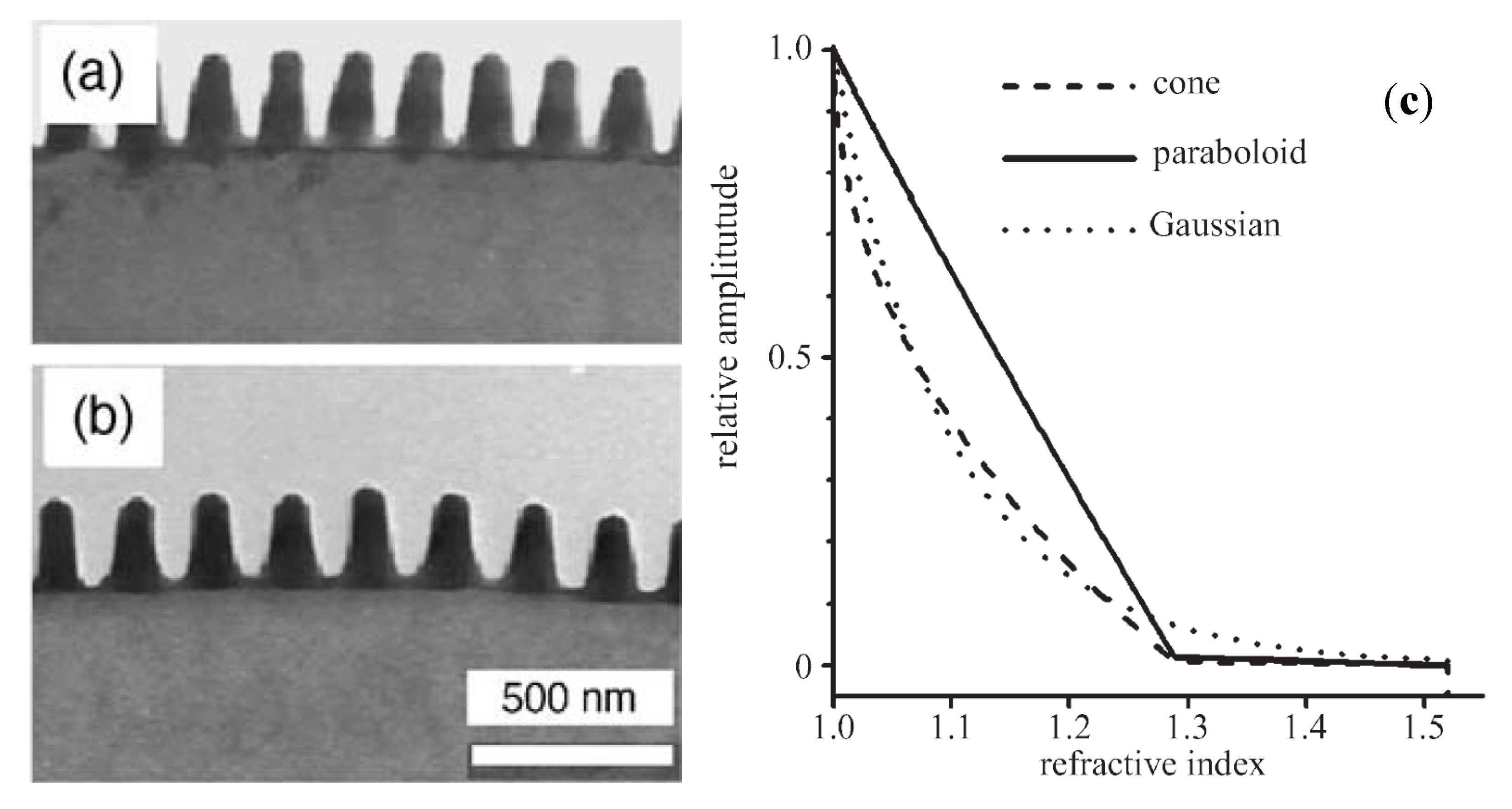
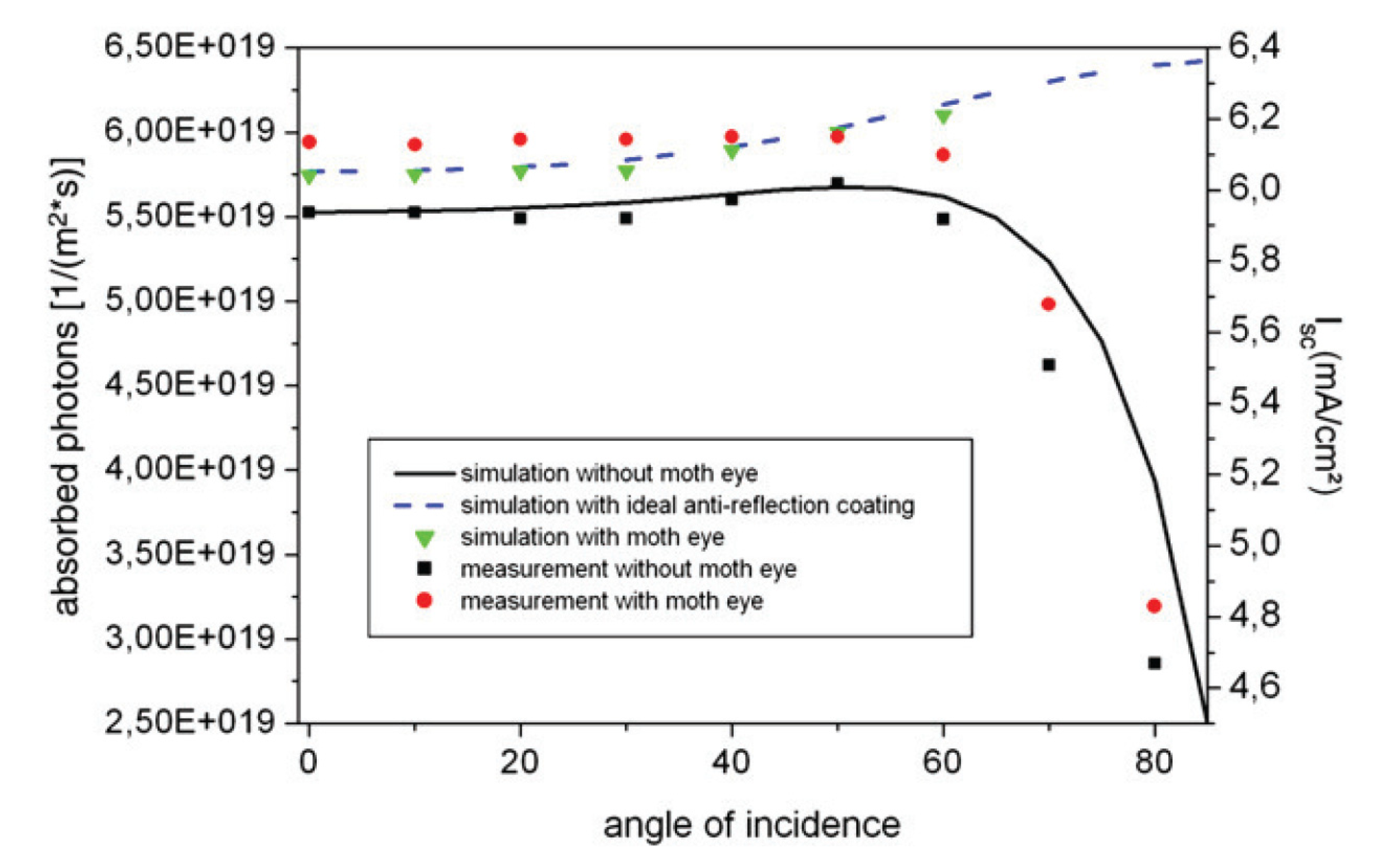
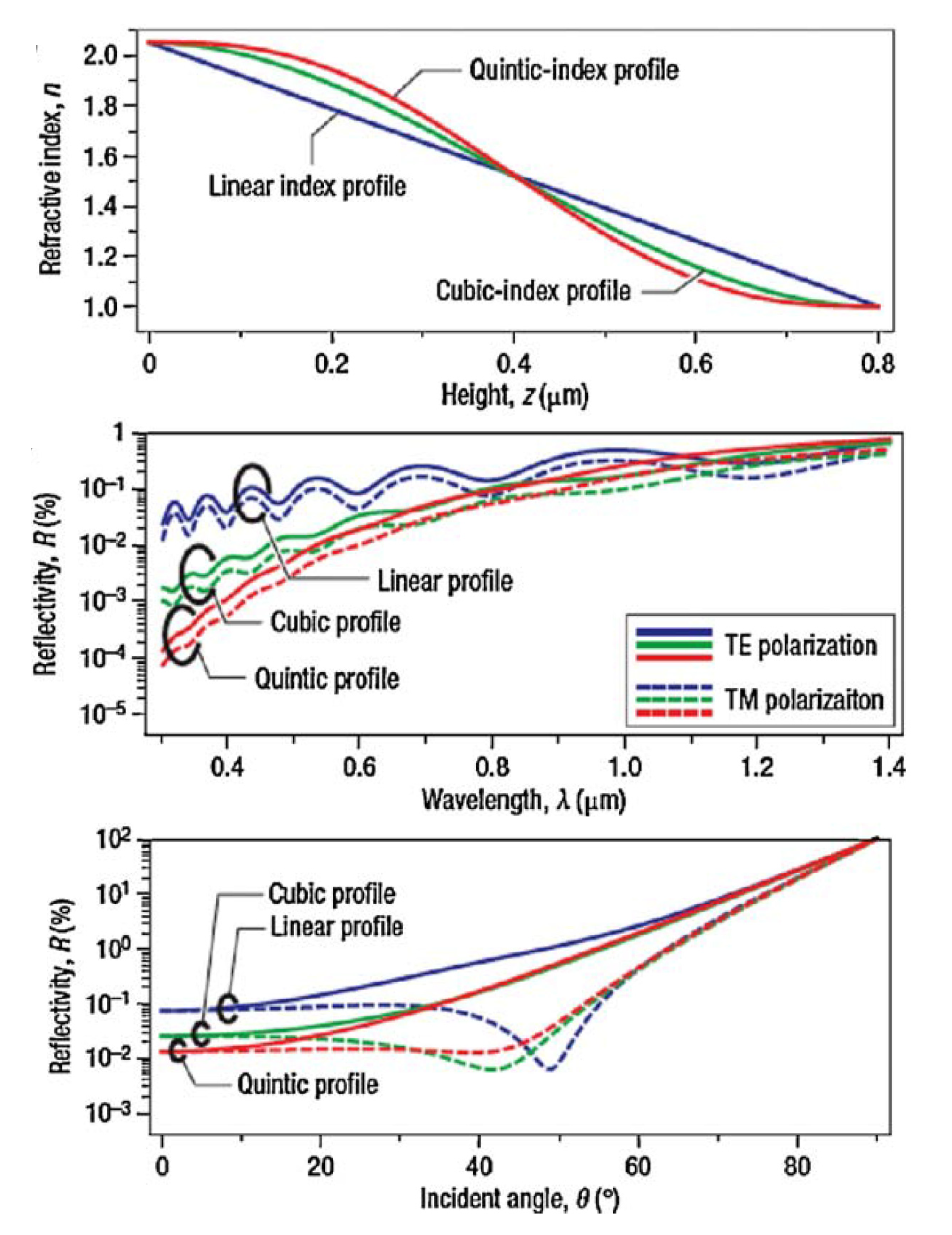
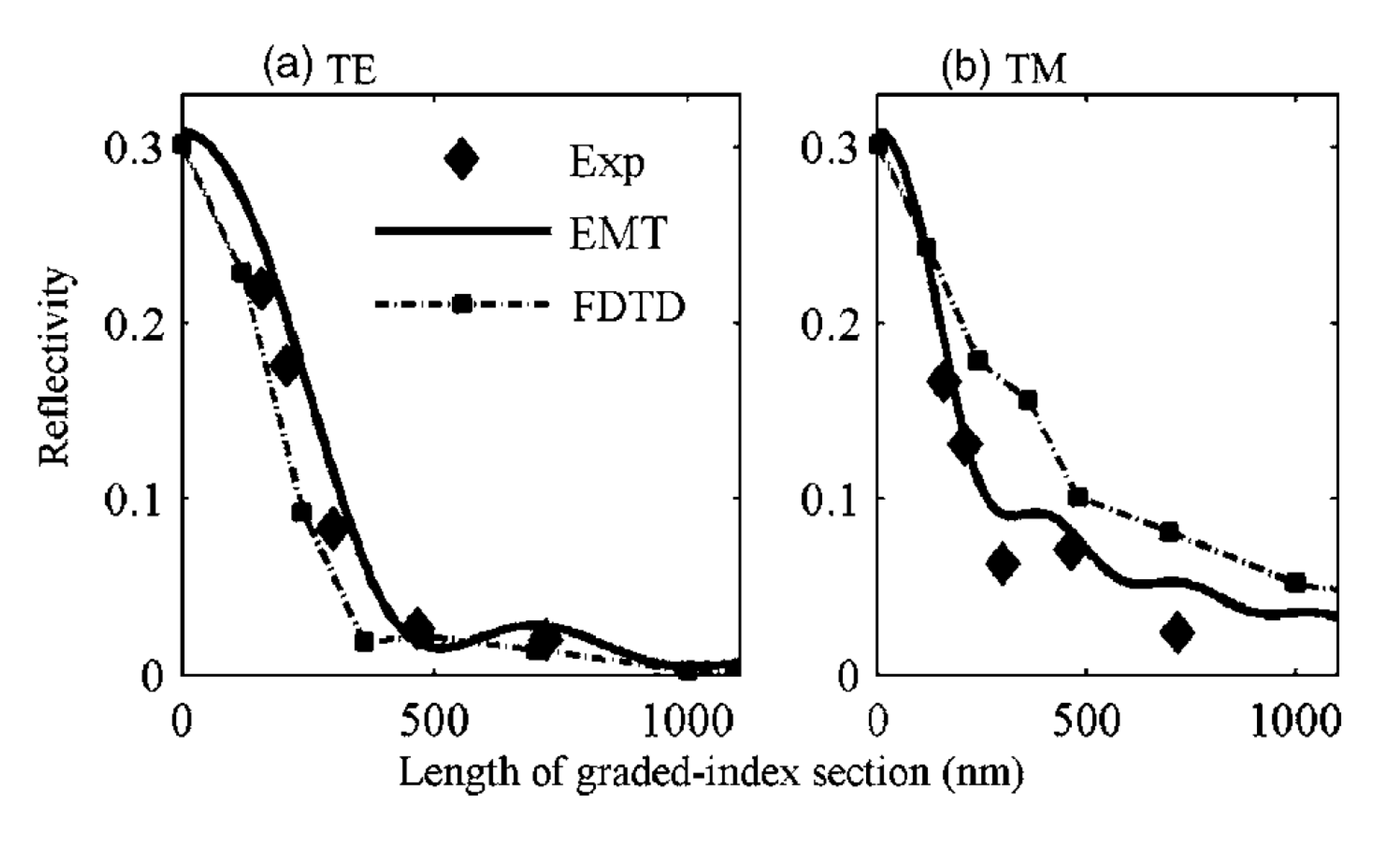
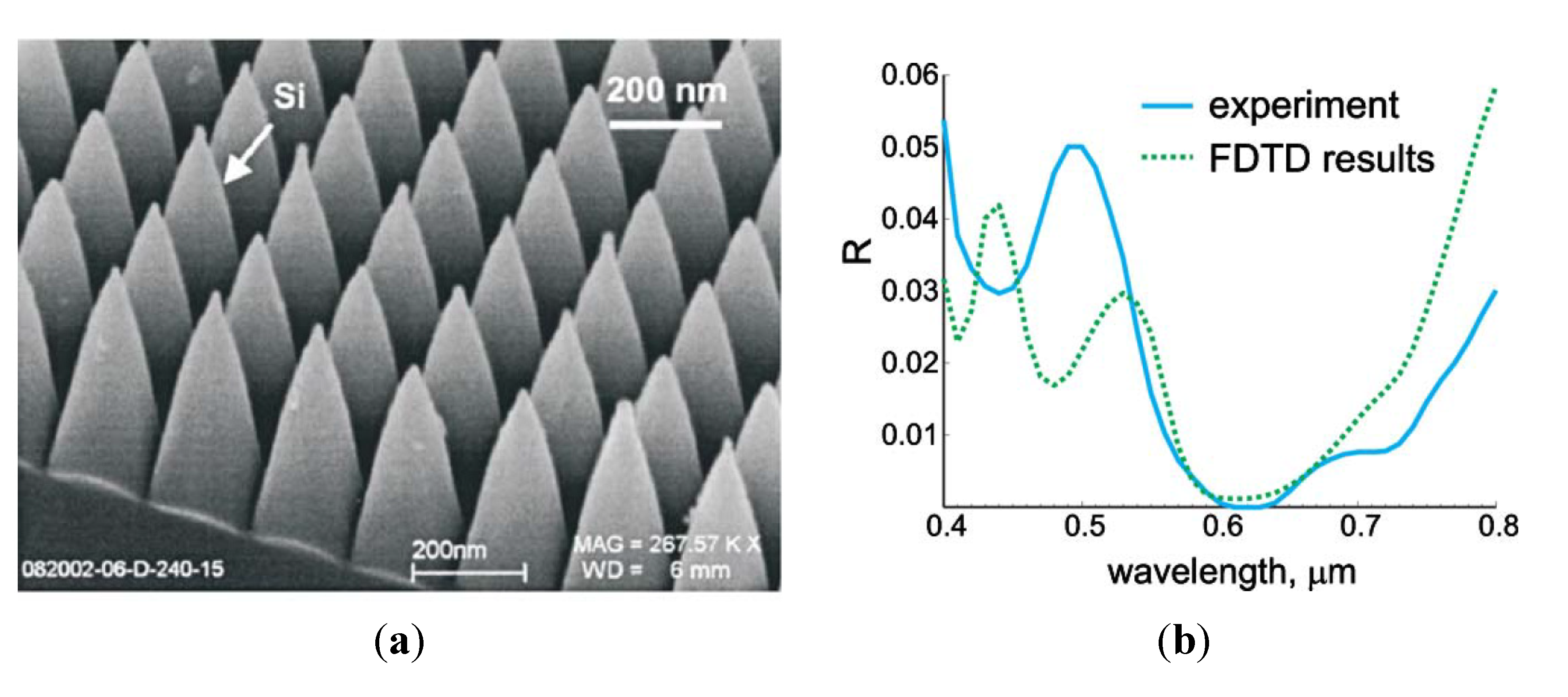
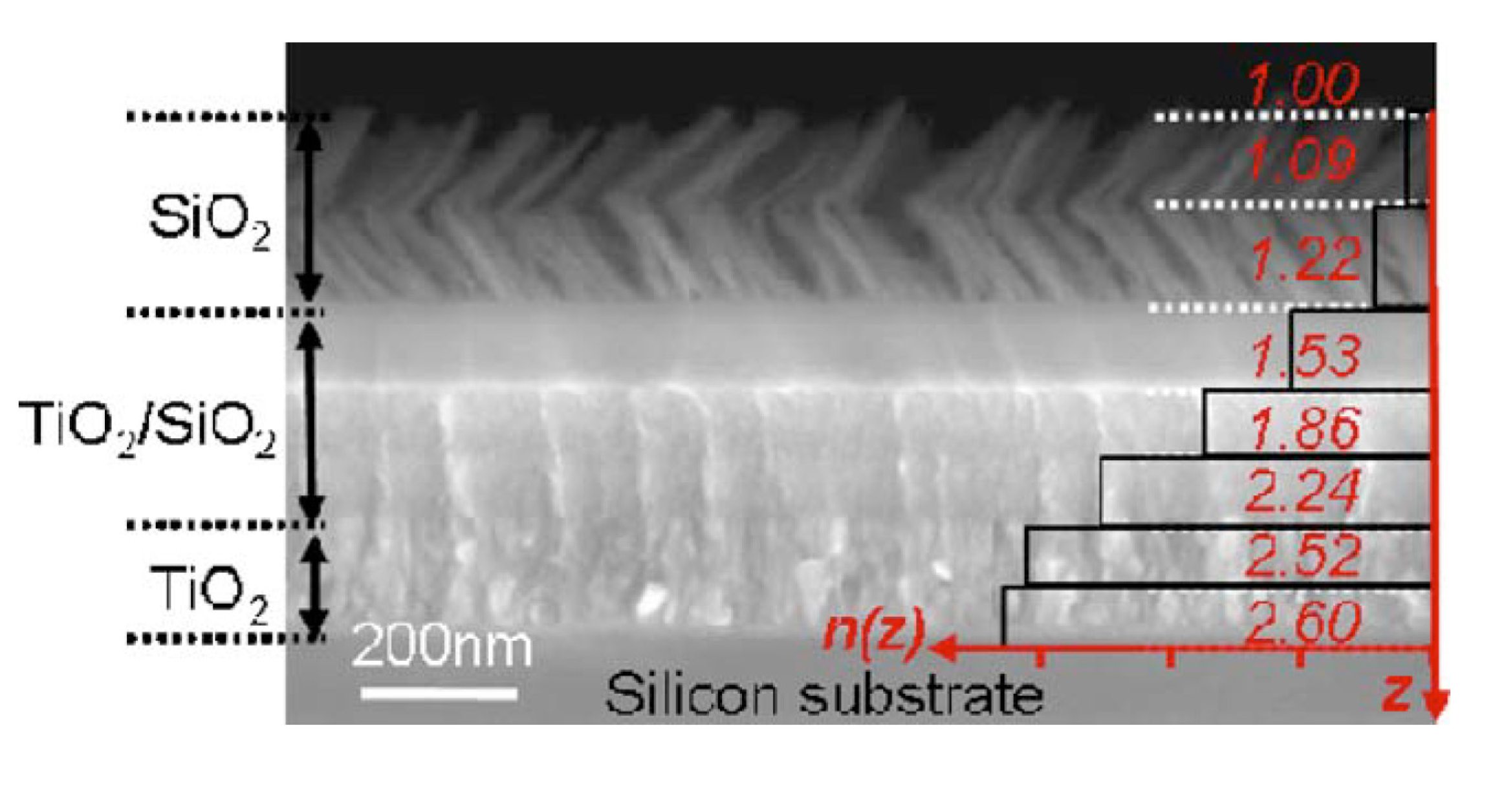
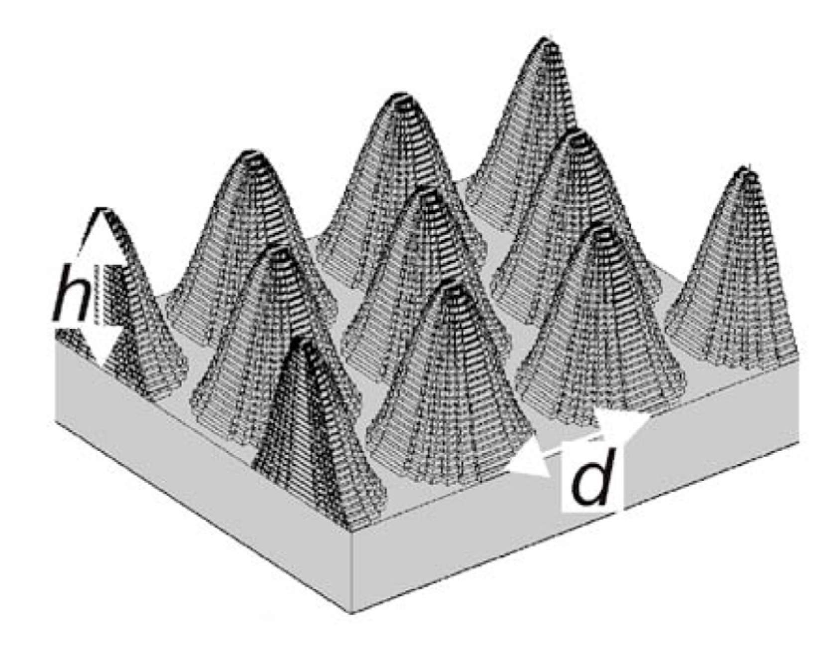
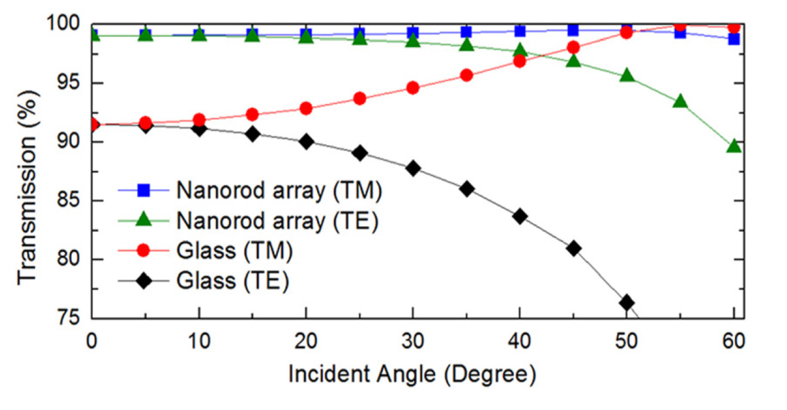
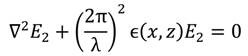
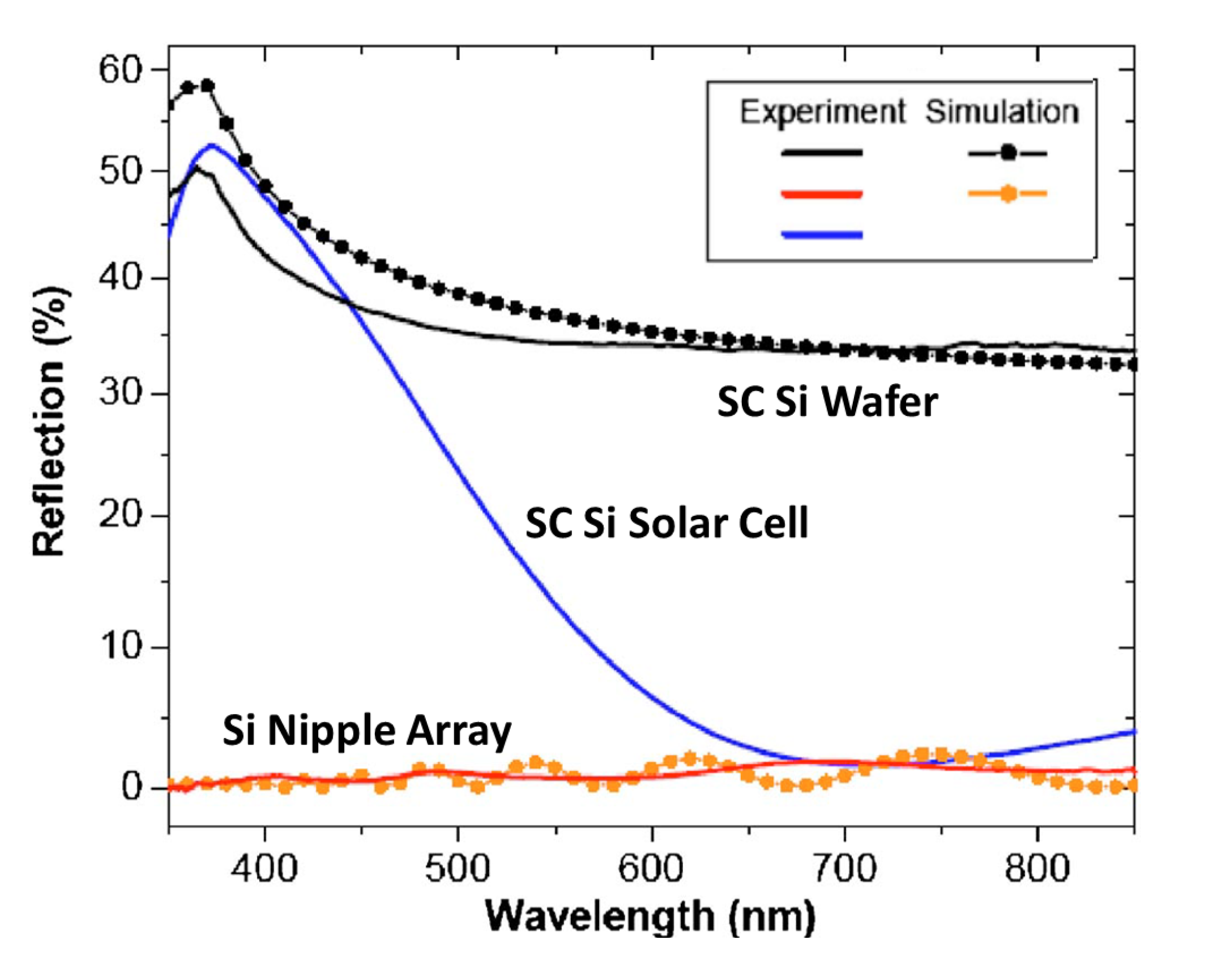
 ), square pyramids with linear and quantic RI profiles closely packed in a square lattice, and cones closely packed in a triangular lattice reported by Deinega et al. [32]. FDTD results are in good agreement with EMT over the wavelengths studied except for very short wavelengths where the assumptions of EMT break down. Separate results comparing FDTD, EMT, and experimental values for reflectivity versus GRIN height are shown in Figure 14.
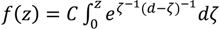 ), square pyramids with linear and quantic RI profiles closely packed in a square lattice, and cones closely packed in a triangular lattice from EMT (lines) and FDTD (points) calculations. Reprinted with permission from reference [32], Copyright 2011 Optical Society of America.
), square pyramids with linear and quantic RI profiles closely packed in a square lattice, and cones closely packed in a triangular lattice from EMT (lines) and FDTD (points) calculations. Reprinted with permission from reference [32], Copyright 2011 Optical Society of America.
), square pyramids with linear and quantic RI profiles closely packed in a square lattice, and cones closely packed in a triangular lattice from EMT (lines) and FDTD (points) calculations. Reprinted with permission from reference [32], Copyright 2011 Optical Society of America.


5. Frequency-Based Optical Modeling Methods
5.1. Transfer Matrix Method


5.2. Rigorous Coupled Wave Analysis, Fourier Modal Method, and Coordinate Transfer Method
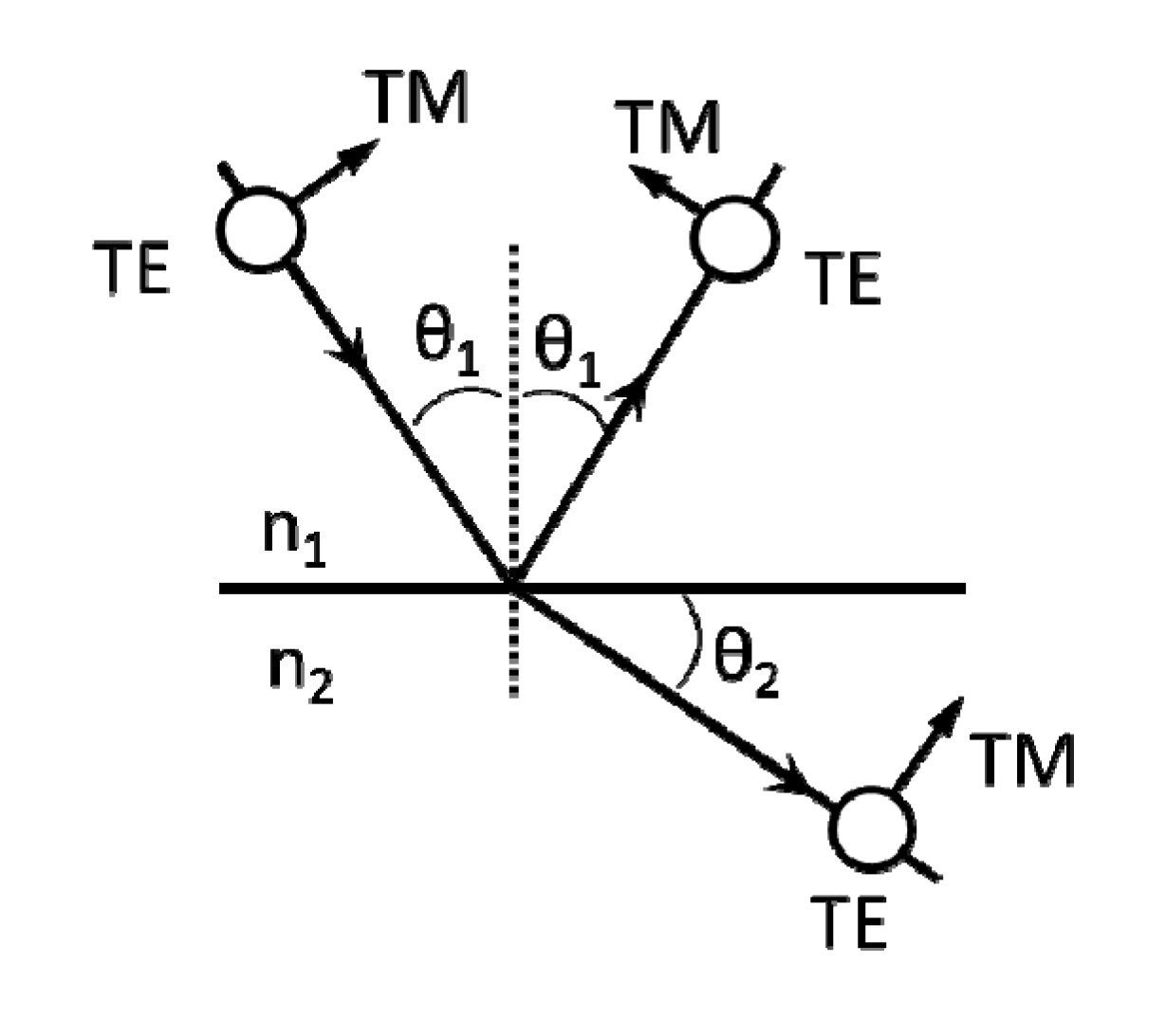
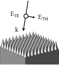
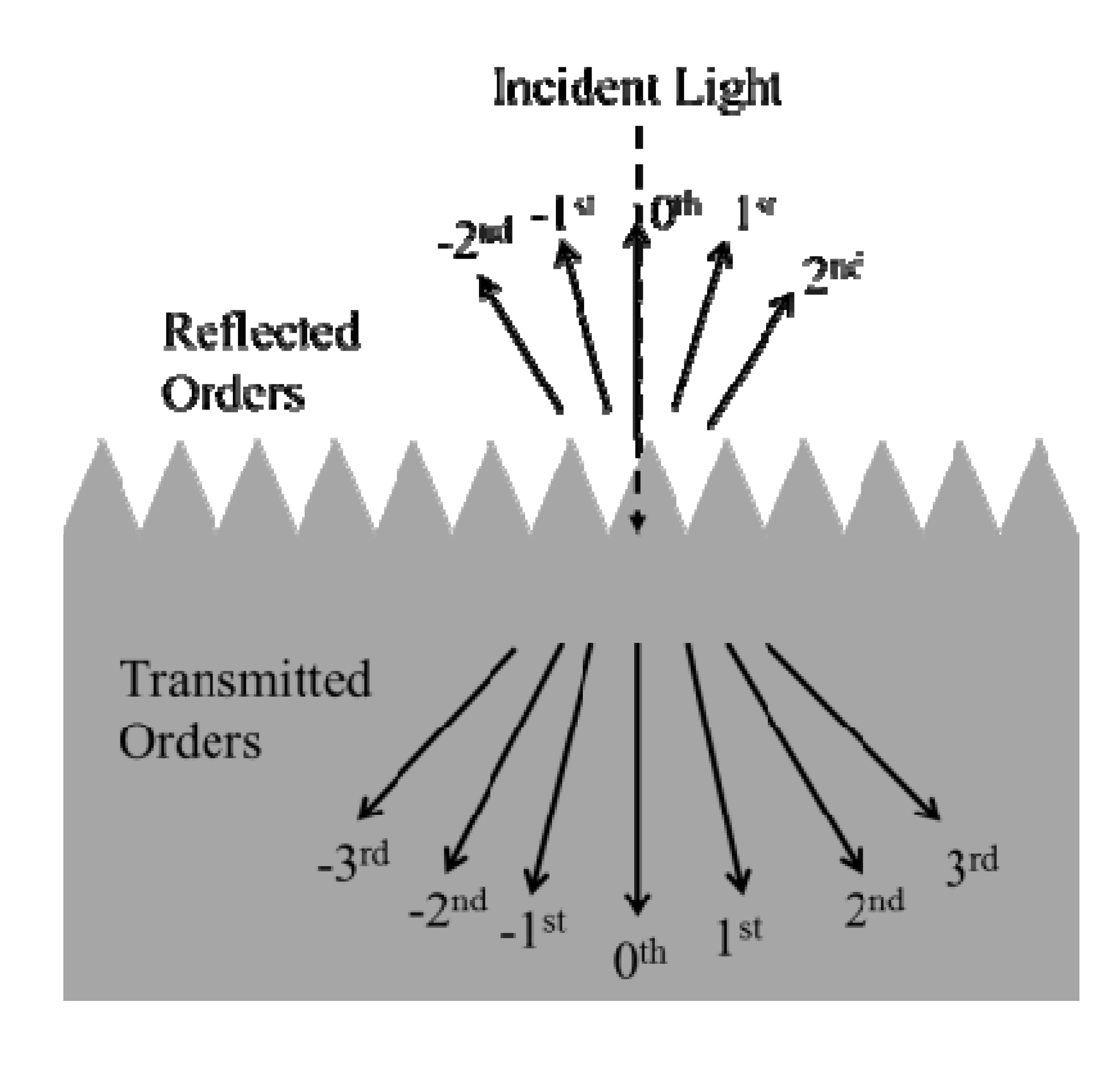
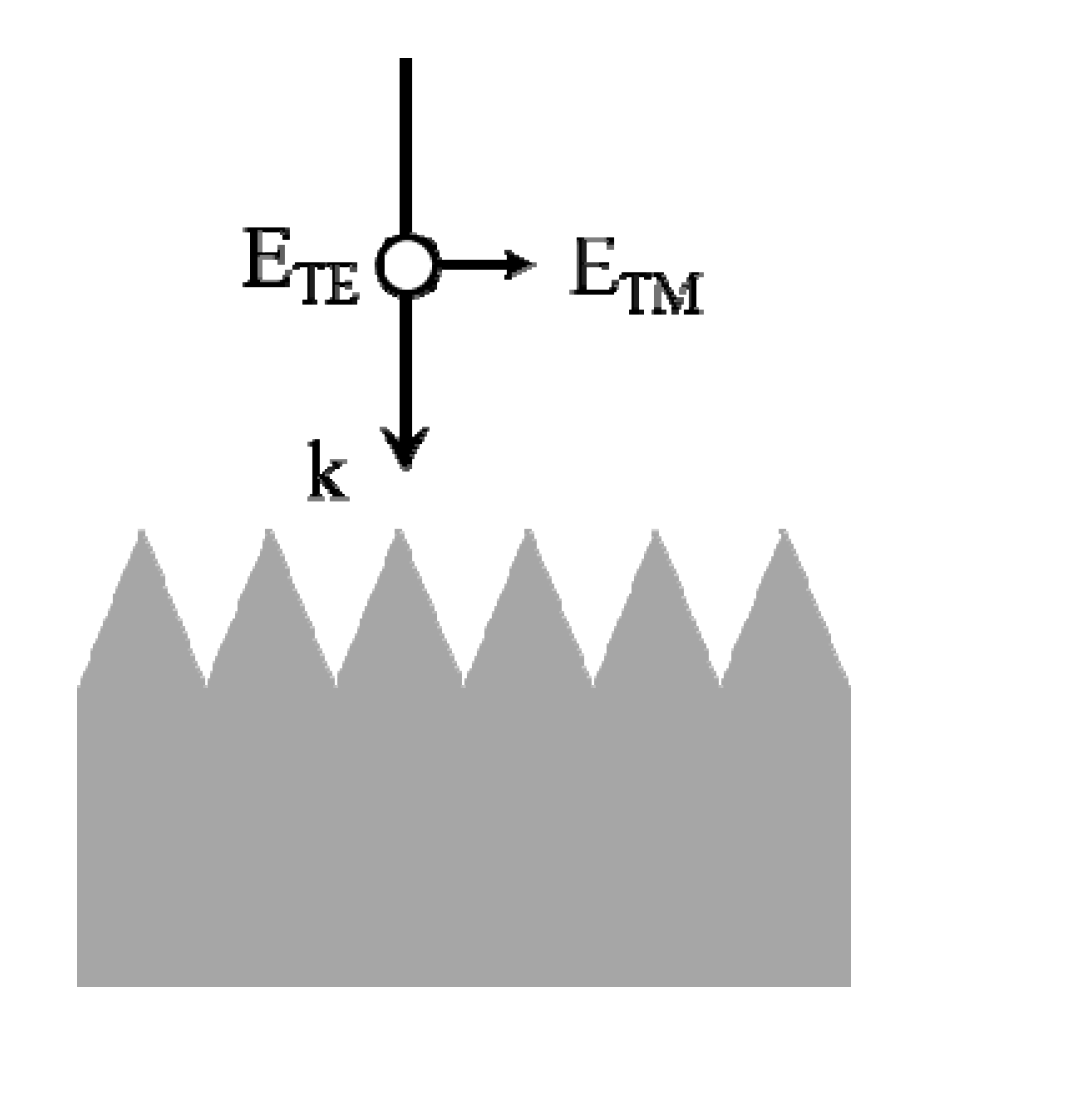
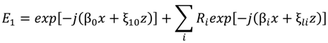
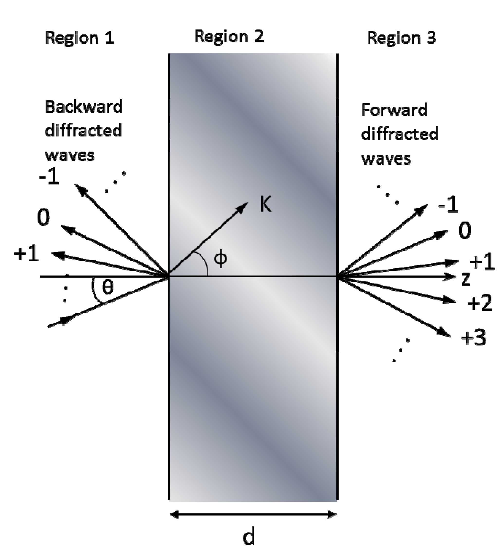
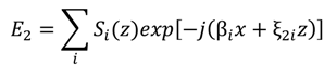
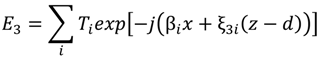
“The rigorous coupled-wave analysis for grating diffraction was first applied to planar (volume) gratings [65]. In these gratings, the refractive index and/or optical absorption vary periodically between the two parallel planar surfaces of the grating. In this method, the field inside the grating is expanded in terms of space-harmonic components that have variable amplitudes in the thickness direction z of the grating. This field expansion together with the Floquet condition (due to the periodic nature of the structure) is then substituted into the appropriate (TE or TM polarization) wave equation, and an infinite set of coupled-wave equations is formed. Using a state space representation, this infinite set of second-order equations is converted into a doubly infinite set of first-order equations. The space-harmonic amplitudes are then solved for in terms of the eigenvalues and eigenvectors of the differential equation coefficient matrix. By applying boundary conditions (continuity of the tangential components of E and H across the boundaries), a set of linear equations is formed. Truncating this set of equations so that an arbitrary level of accuracy is achieved, the amplitudes of the propagating diffracted orders and the evanescent orders may then be determined. From the amplitudes of the propagating orders, the diffraction efficiencies may be directly calculated. None of the common approximations (neglect of second derivatives, neglect of boundary effects, neglect of higher-order waves, neglect of dephasing from the Bragg angle, or small grating modulation) is used in this analysis. The method is rigorous, and any specified level of accuracy can be obtained.Rigorous coupled-wave analysis has also been applied to surface-relief gratings [66]. In this case, the surface-relief grating is divided into a large number of thin layers parallel to the surface. Each thin layer grating is analyzed using the state variables method described above and then by applying the boundary conditions to the boundaries of each layer, it is possible to obtain the forward- and backward-diffracted wave amplitudes.”


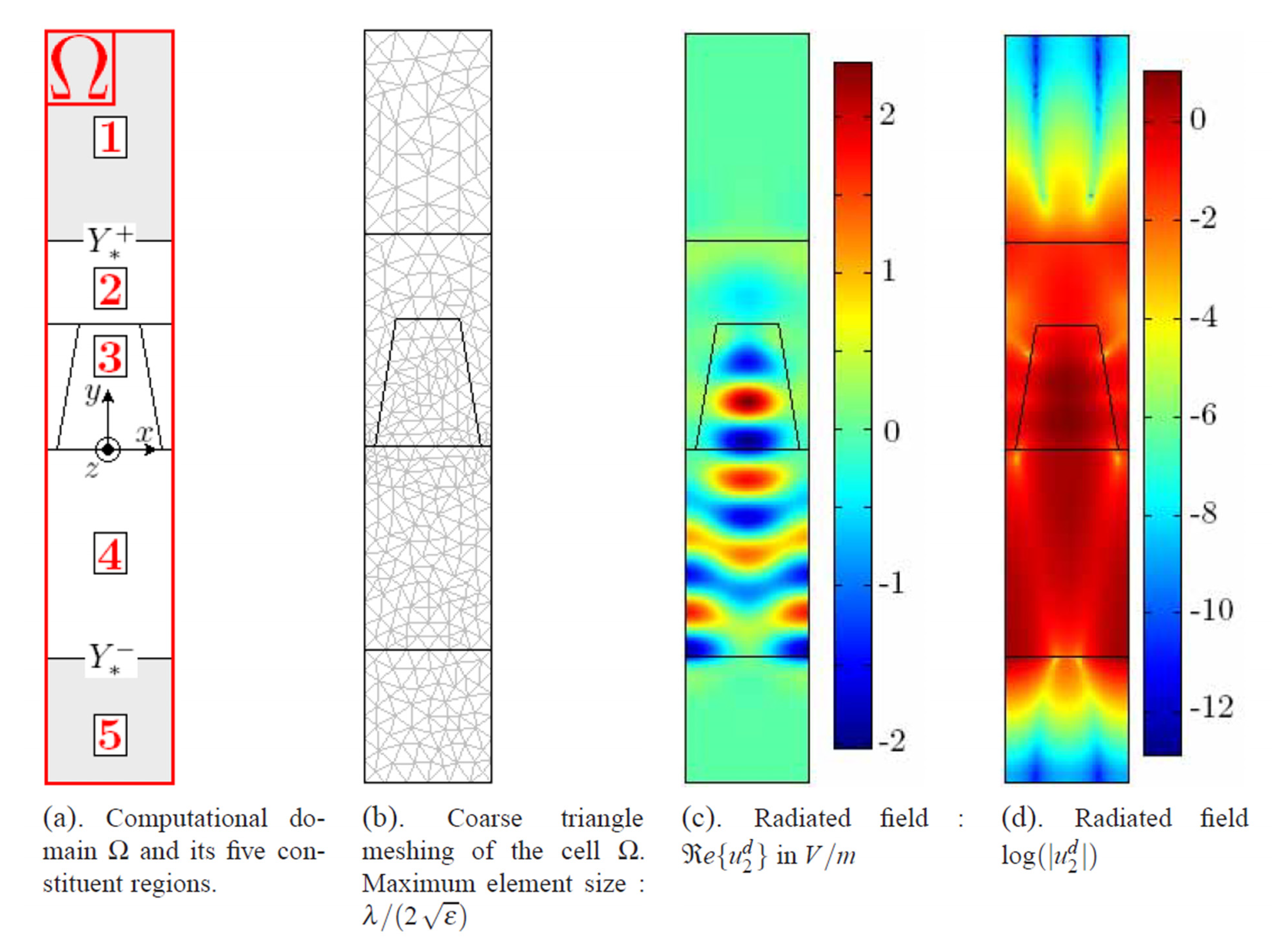
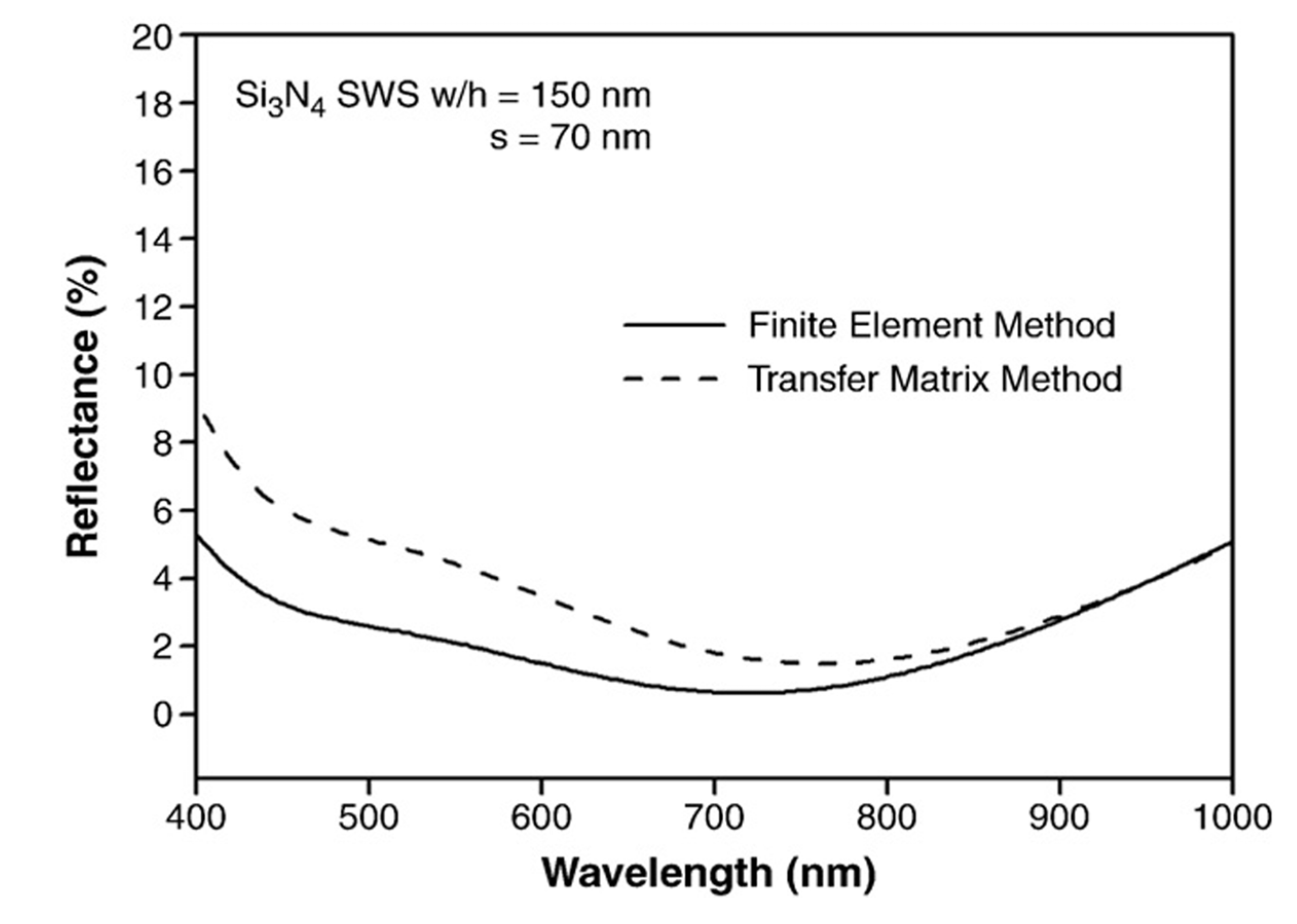
5.3. Finite Element Method


6. Conclusions
| Features | FDTD | FEM | TMM | FMM/RCWA |
|---|---|---|---|---|
| Geometry Restrictions | None | None | Thin Films Only | Not efficient for aperiodic surfaces |
| Time or Frequency Based | Time | Frequency | Frequency | Frequency |
| Output | Field Strengths | Field Strengths | %R/%T | %R/%T |
| Spatially discretized | Yes | Yes | No | No |
| Models dispersion naturally | No | Yes | Yes | Yes |
| Multiple wavelengths per simulation | Yes | No | No | No |
| Rigorous | Yes | Yes | Yes | Yes |
| Anisotropic gratings | Yes | Yes | No | Yes |
| Computation Speed | Slow | Meshing slow, computation fast | Fast | Medium |
| Source of Inaccuracies | Discretization of geometry and rounding error | Discretization of geometry and rounding error | EMT or slicing of geometry into layers | Truncation of Fourier series expansions for field values, permittivity and truncation of orders of diffracted light |
| Numerical convergence | Difficult for some metals, dispersion, and wavelength-sized features | Good | Good | Difficult for TM polarization |
| Maximum Dimensions | 3D | 3D | 1D | 3D |
Supplementary Materials
Supplementary File 1Acknowledgments
Conflicts of Interest
References
- Nevière, M.; Popov, E. Light Propagation in Periodic Media: Differential Theory and Design; CRC Press: New York, NY, USA, 2003. [Google Scholar]
- Novotny, L.; Hecht, B. Principles of Nano-Optics; Cambridge University Press: New York, NY, USA, 2012. [Google Scholar]
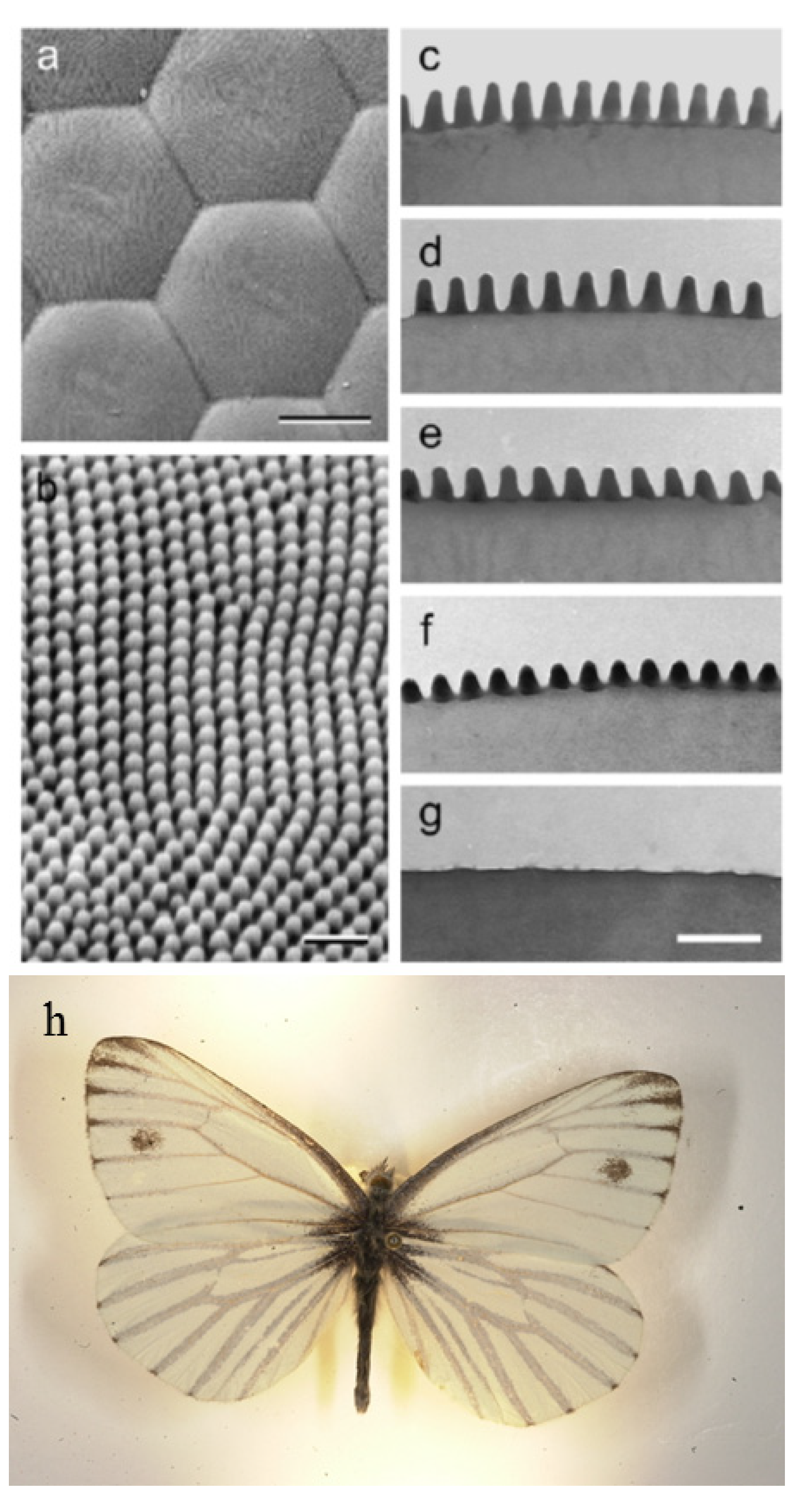
- Stavenga, D.G.; Foletti, S.; Palasantzas, G.; Arikawa, K. Light on the moth-eye corneal nipple array of butterflies. Proc. R. Soc. B 2006, 273, 661–667. [Google Scholar] [CrossRef]
- Stavenga, D.G.; Arikawa, K. Evolution of color and vision of butterflies. Arthropod Struct. Dev. 2006, 35, 307–318. [Google Scholar] [CrossRef]
- Discover Life Homepage. Available online: http://www.discoverlife.org (accessed on 28 December 2013).
- Chattopadhyay, S.; Huang, Y.F.; Jen, Y.J.; Ganguly, A.; Chen, K.H.; Chen, L.C. Anti-reflecting and photonic nanostructures. Mater. Sci. Eng. R 2010, 69, 1–35. [Google Scholar] [CrossRef]
- Chen, H.L.; Chuang, S.Y.; Lin, C.H.; Lin, Y.H. Using colloidal lithography to fabricate and optimize sub-wavelength pyramidal and honeycomb structures in solar cells. Opt. Express 2007, 15, 14793–14803. [Google Scholar] [CrossRef]
- Chuang, S.Y.; Chen, H.L.; Shieh, J.; Lin, C.H.; Cheng, C.C.; Liu, H.W.; Yu, C.C. Nanoscale of biomimetic moth eye structures exhibiting inverse polarization phenomena at the brewster angle. Nanoscale 2010, 2, 799–805. [Google Scholar] [CrossRef]
- Knop, K. Rigorous diffraction theory for transmission phase gratings with deep rectangular grooves. JOSA 1978, 68, 1206–1210. [Google Scholar] [CrossRef]
- Sheng, P.; Stepleman, R.; Sanda, P. Exact eigenfunctions for square-wave gratings: Application to diffraction and surface-plasmon calculations. Phys. Rev. B 1982, 26, 2907–2916. [Google Scholar] [CrossRef]
- Bouffaron, R.; Escoubas, L.; Simon, J.J.; Torchio, P.; Flory, F.; Berginc, G.; Masclet, P. Enhanced antireflecting properties of micro-structured top-flat pyramids. Opt. Express 2008, 16, 19304–19309. [Google Scholar] [CrossRef]
- Chang, Y.C.; Mei, G.H.; Chang, T.W.; Wang, T.J.; Lin, D.Z.; Lee, C.K. Design and fabrication of a nanostructured surface combining antireflective and enhanced-hydrophobic effects. Nanotechnology 2007, 18. [Google Scholar] [CrossRef]
- Rytov, S. Electromagnetic properties of a finely stratified medium. Sov. Phys. JETP 1956, 2, 466–475. [Google Scholar]
- Brundrett, D.L.; Glytsis, E.N.; Gaylord, T.K. Homogeneous layer models for high-spatial-frequency dielectric surface-relief gratings: Conical diffraction and antireflection designs. Appl. Opt. 1994, 33, 2695–2706. [Google Scholar] [CrossRef]
- Lalanne, P.; Lemercier-Lalanne, D. On the effective medium theory of subwavelength periodic structures. J. Mod. Opt. 1996, 43, 2063–2085. [Google Scholar] [CrossRef]
- Garnett, J.C.M. Colours in metal glasses and in metallic films. Phil. Trans. R. Soc. A 1904, 203, 385–420. [Google Scholar] [CrossRef]
- Aspnes, D. Local-field effects and effective-medium theory: A microscopic perspective. Am. J. Phys. 1982, 50, 704–709. [Google Scholar] [CrossRef]
- Garnett, J.M. Colours in metal glasses, in metallic films, and in metallic solutions. II. Philos. Trans. R. Soc. A 1906, 205, 237–288. [Google Scholar] [CrossRef]
- Bruggeman, V.D. Berechnung verschiedener physikalischer konstanten von heterogenen substanzen. I. Dielektrizitätskonstanten und leitfähigkeiten der mischkörper aus isotropen substanzen. Ann. Phys. 1935, 416, 636–664. (in German). [Google Scholar] [CrossRef]
- Forberich, K.; Dennler, G.; Scharber, M.C.; Hingerl, K.; Fromherz, T.; Brabec, C.J. Performance improvement of organic solar cells with moth eye anti-reflection coating. Thin Solid Films 2008, 516, 7167–7170. [Google Scholar] [CrossRef]
- Brunner, R.; Sandfuchs, O.; Pacholski, C.; Morhard, C.; Spatz, J. Lessons from nature: Biomimetic subwavelength structures for high-performance optics. Laser Photonics Rev. 2012, 6, 641–659. [Google Scholar] [CrossRef]
- Haidar, R.; Vincent, G.; Guerineau, N.; Collin, S.; Velghe, S.; Primot, J. Wollaston prism-like devices based on blazed dielectric subwavelength gratings. Opt. Express 2005, 13, 9941–9953. [Google Scholar] [CrossRef]
- Xi, J.Q.; Schubert, M.F.; Kim, J.K.; Schubert, E.F.; Chen, M.F.; Lin, S.Y.; Liu, W.; Smart, J.A. Optical thin-film materials with low refractive index for broadband elimination of fresnel reflection. Nat. Photonics 2007, 1, 176–179. [Google Scholar]
- Yee, K.S. Numerical solution of initial boundary value problems involving maxwell’s equations in isotropic media. IEEE Trans. Antennas Propag. 1966, 14, 302–307. [Google Scholar] [CrossRef]
- Taflove, A.; Brodwin, M.E. Numerical-solution of steady-state electromagnetic scattering problems using time-dependent maxwells equations. IEEE Trans. Microw. Theory Tech. 1975, 23, 623–630. [Google Scholar] [CrossRef]
- Taflove, A.; Hagness, S.C. Computational Electrodynamics: The Finite-Difference Time-Domain Method, 3rd ed.; Artech House, Inc.: Norwood, MA, USA, 2005. [Google Scholar]
- Yamauchi, J.; Mita, M.; Aoki, S.; Nakano, H. Analysis of antireflection coatings using the FD-TD method with the PML absorbing boundary condition. IEEE Photonics Technol. Lett. 1996, 8, 239–241. [Google Scholar] [CrossRef]
- Yamauchi, J.; Ando, T.; Nakano, H. Analysis of dielectric hollow slab wave-guides using the finite-difference beam-propagation method. IEICE Trans. Electron. 1993, E76C, 1695–1697. [Google Scholar]
- Yang, Z.Y.; Zhu, D.Q.; Zhao, M.; Cao, M.C. The study of a nano-porous optical film with the finite difference time domain method. J. Opt. A Pure Appl. Opt. 2004, 6, 564–568. [Google Scholar] [CrossRef]
- Tsai, H.Y. Finite difference time domain analysis of three-dimensional sub-wavelength structured arrays. Jpn. J. Appl. Phys. 2008, 47, 5007–5009. [Google Scholar] [CrossRef]
- Berenger, J.P. A perfectly matched layer for the absorption of electromagnetic-waves. J. Comput. Phys. 1994, 114, 185–200. [Google Scholar] [CrossRef]
- Deinega, A.; Valuev, I.; Potapkin, B.; Lozovik, Y. Minimizing light reflection from dielectric textured surfaces. J. Opt. Soc. Am. A 2011, 28, 770–777. [Google Scholar] [CrossRef]
- Deinega, A.V.; Konistyapina, I.V.; Bogdanova, M.V.; Valuev, I.A.; Lozovik, Y.E.; Potapkin, B.V. Optimization of an anti-reflective layer of solar panels based on ab initio calculations. Russ. Phys. J. 2009, 52, 1128–1134. [Google Scholar] [CrossRef]
- Ting, C.J.; Chen, C.F.; Chou, C.P. Antireflection subwavelength structures analyzed by using the finite difference time domain method. Optik 2009, 120, 814–817. [Google Scholar] [CrossRef]
- Chou, T.H.; Cheng, K.Y.; Chang, T.L.; Ting, C.J.; Hsu, H.C.; Wu, C.J.; Tsai, J.H.; Huang, T.Y. Fabrication of antireflection structures on tco film for reflective liquid crystal display. Microelectron. Eng. 2009, 86, 628–631. [Google Scholar] [CrossRef]
- Feng, N.N.; Zhou, G.R.; Huang, W.P. Space mapping technique for design optimization of antireflection coatings in photonic devices. J. Lightwave Technol. 2003, 21, 281–285. [Google Scholar] [CrossRef]
- Li, Z.F.; Ozbay, E.; Chen, H.B.; Chen, J.J.; Yang, F.H.; Zheng, H.Z. Resonant cavity based compact efficient antireflection structures for photonic crystals. J. Phys. D 2007, 40, 5873–5877. [Google Scholar]
- Zhou, G.R.; Li, X.; Feng, N.N. Design of deeply etched antireflective waveguide terminators. IEEE J. Quantum Electron. 2003, 39, 384–391. [Google Scholar] [CrossRef]
- Deinega, A.; Valuev, I.; Potapkin, B.; Lozovik, Y. Antireflective properties of pyramidally textured surfaces. Opt. Lett. 2010, 35, 106–108. [Google Scholar] [CrossRef]
- Schmid, J.H.; Cheben, P.; Janz, S.; Lapointe, J.; Post, E.; Xu, D.X. Gradient-index antireflective subwavelength structures for planar waveguide facets. Opt. Lett. 2007, 32, 1794–1796. [Google Scholar] [CrossRef]
- Catchpole, K.R.; Mokkapati, S.; Beck, F.; Wang, E.C.; McKinley, A.; Basch, A.; Lee, J. Plasmonics and nanophotonics for photovoltaics. MRS Bull. 2011, 36, 461–467. [Google Scholar] [CrossRef]
- Ichikawa, H. Subwavelength triangular random gratings. J. Mod. Opt. 2002, 49, 1893–1906. [Google Scholar] [CrossRef]
- Ting, C.J.; Chen, C.F.; Hsu, C.J. Subwavelength structured surfaces with a broadband antireflection function analyzed by using a finite difference time domain method. Optik 2010, 121, 1069–1074. [Google Scholar] [CrossRef]
- Park, H.; Shin, D.; Kang, G.; Baek, S.; Kim, K.; Padilla, W.J. Broadband optical antireflection enhancement by integrating antireflective nanoislands with silicon nanoconical-frustum arrays. Adv. Mater. 2011, 23, 5796–5800. [Google Scholar] [CrossRef]
- Ting, C.J.; Chen, C.F.; Chou, C.P. Subwavelength structures for broadband antireflection application. Opt. Commun. 2009, 282, 434–438. [Google Scholar] [CrossRef]
- Son, J.; Verma, L.K.; Danner, A.J.; Bhatia, C.S.; Yang, H. Enhancement of optical transmission with random nanohole structures. Opt. Express 2011, 19, A35–A40. [Google Scholar] [CrossRef]
- Deniz, H.; Khudiyev, T.; Buyukserin, F.; Bayindir, M. Room temperature large-area nanoimprinting for broadband biomimetic antireflection surfaces. Appl. Phys. Lett. 2011, 99, 183107:1–183107:3. [Google Scholar]
- Yi, J.; Lee, D.H.; Park, W.I. Site-specific design of cone-shaped Si nanowires by exploiting nanoscale surface diffusion for optimal photoabsorption. Chem. Mater. 2011, 23, 3902–3906. [Google Scholar] [CrossRef]
- Ting, C.J.; Chang, F.Y.; Chen, C.F.; Chou, C.P. Fabrication of an antireflective polymer optical film with subwavelength structures using a roll-to-roll micro-replication process. J. Micromech. Microeng. 2008, 18. [Google Scholar] [CrossRef]
- Mokkapati, S.; Beck, F.J.; Polman, A.; Catchpole, K.R. Designing periodic arrays of metal nanoparticles for light-trapping applications in solar cells. Appl. Phys. Lett. 2009, 95. [Google Scholar] [CrossRef]
- Mokkapati, S.; Beck, F.J.; de Waele, R.; Polman, A.; Catchpole, K.R. Resonant nano-antennas for light trapping in plasmonic solar cells. J. Phys. D 2011, 44. [Google Scholar] [CrossRef]
- Nagel, J.R.; Scarpulla, M.A. Enhanced absorption in optically thin solar cells by scattering from embedded dielectric nanoparticles. Opt. Express 2010, 18, A139–A146. [Google Scholar]
- Du, Y.; Liu, S.J.; He, H.B.; Jin, Y.X.; Kong, F.Y.; Guan, H.Y. Laser-induced damage properties of antireflective porous glasses. Opt. Commun. 2012, 285, 5512–5518. [Google Scholar] [CrossRef]
- Wang, L.; Xu, B.B.; Chen, Q.D.; Ma, Z.C.; Zhang, R.; Liu, Q.X.; Sun, H.B. Maskless laser tailoring of conical pillar arrays for antireflective biomimetic surfaces. Opt. Lett. 2011, 36, 3305–3307. [Google Scholar] [CrossRef]
- Isabella, O.; Solntsev, S.; Caratelli, D.; Zeman, M. 3-D optical modeling of thin-film silicon solar cells on diffraction gratings. Prog. Photovolt. 2013, 21, 94–108. [Google Scholar] [CrossRef]
- Hecht, E.; Ganesan, A. Optics; Pearson Education: San Francisco, CA, USA, 2002. [Google Scholar]
- Condon, E.U.; Odishaw, H. Handbook of Physics; Springer: New York, NY, USA, 1967. [Google Scholar]
- Abelès, F. La théorie générale des couches minces. J. Phys. Radium 1950, 11, 307–309. [Google Scholar] [CrossRef]
- Boden, S.A.; Bagnall, D.M. Sunrise to sunset optimization of thin film antireflective coatings for encapsulated, planar silicon solar cells. Prog. Photovolt. 2009, 17, 241–252. [Google Scholar] [CrossRef]
- Boden, S.A.; Bagnall, D.M. Bio-Mimetic Subwavelength Surfaces for Near-Zero Reflection Sunrise to Sunset. In Proceedings of the Conference Record of the 2006 IEEE 4th World Conference on Photovoltaic Energy Conversion, Waikoloa, HI, USA, 7–12 May 2006; pp. 1358–1361.
- Kuo, M.L.; Poxson, D.J.; Kim, Y.S.; Mont, F.W.; Kim, L.K.; Schuhert, E.F.; Lin, S.Y. Realization of a near-perfect antireflection coating for silicon solar energy utilization. Opt. Lett. 2008, 33, 2527–2529. [Google Scholar] [CrossRef]
- Kim, H.; Lee, I.M.; Lee, B. Extended scattering-matrix method for efficient full parallel implementation of rigorous coupled-wave analysis. J. Opt. Soc. Am. A 2007, 24, 2313–2327. [Google Scholar] [CrossRef]
- Hench, J.J.; Strakos, Z. The rcwa method—A case study with open questions and perspectives of algebraic computations. Electron. Trans. Numer. Anal. 2008, 31, 331–357. [Google Scholar]
- Gaylord, T.K.; Baird, W.E.; Moharam, M.G. Zero-reflectivity high spacial-frequency rectangular-groove dielectric surface-relief gratings. Appl. Opt. 1986, 25, 4562–4567. [Google Scholar] [CrossRef]
- Moharam, M.; Gaylord, T. Rigorous coupled-wave analysis of planar-grating diffraction. J. Opt. Soc. Am. 1981, 71, 811–818. [Google Scholar] [CrossRef]
- Moharam, M.G.; Gaylord, T.K. Diffraction analysis of dielectric surface-relief gratings. J. Opt. Soc. Am. 1982, 72, 1385–1392. [Google Scholar] [CrossRef]
- Mirotznik, M.S.; Good, B.L.; Ransom, P.; Wikner, D.; Mait, J.N. Broadband antireflective properties of inverse motheye surfaces. IEEE Trans. Antennas Propag. 2010, 58, 2969–2980. [Google Scholar] [CrossRef]
- Jing, X.F.; Shao, P.D.; Jin, Y.X.; Fan, Z.X. Near-field distribution of broadband antireflective nanostructure arrays. Optik 2012, 123, 527–533. [Google Scholar] [CrossRef]
- Jing, X.F.; Tian, Y.; Han, J.L.; Ma, J.Y.; Jin, Y.X.; Shao, J.D.; Fan, Z.X. Polarization effect of femtosecond pulse breakdown in subwavelength antireflective relief grating. Opt. Commun. 2011, 284, 4220–4224. [Google Scholar] [CrossRef]
- Li, L. Formulation and comparison of two recursive matrix algorithms for modeling layered diffraction gratings. J. Opt. Soc. Am. A 1996, 13, 1024–1035. [Google Scholar] [CrossRef]
- Li, L.F. New formulation of the fourier modal method for crossed surface-relief gratings. J. Opt. Soc. Am. A 1997, 14, 2758–2767. [Google Scholar] [CrossRef]
- Boden, S.A.; Bagnall, D.M. Tunable reflection minima of nanostructured antireflective surfaces. Appl. Phys. Lett. 2008, 93, 133108:1–133108:3. [Google Scholar]
- Li, L.F. Use of fourier series in the analysis of discontinuous periodic structures. J. Opt. Soc. Am. A 1996, 13, 1870–1876. [Google Scholar] [CrossRef]
- Aryal, M.; Ko, D.H.; Tumbleston, J.R.; Gadisa, A.; Samulski, E.T.; Lopez, R. Large area nanofabrication of butterfly wing’s three dimensional ultrastructures. J. Vac. Sci. Technol. B 2012, 30, 061802:1–061802:7. [Google Scholar]
- Boden, S.A.; Bagnall, D.M. Optimization of moth-eye antireflection schemes for silicon solar cells. Prog. Photovolt. 2010, 18, 195–203. [Google Scholar] [CrossRef]
- Leem, J.W.; Yu, J.S. Indium tin oxide subwavelength nanostructures with surface antireflection and superhydrophilicity for high-efficiency Si-based thin film solar cells. Opt. Express 2012, 20, A431–A440. [Google Scholar] [CrossRef]
- Leem, J.W.; Yu, J.S. Multi-functional antireflective surface-relief structures based on nanoscale porous germanium with graded refractive index profiles. Nanoscale 2013, 5, 2520–2526. [Google Scholar] [CrossRef]
- Mizutani, A.; Kobayashi, Y.; Maruyama, A.; Kikuta, H. Ray tracing of an aspherical lens with antireflective subwavelength structured surfaces. J. Opt. Soc. Am. A 2009, 26, 337–341. [Google Scholar]
- Park, B.D.; Leem, J.W.; Yu, J.S. Bioinspired Si subwavelength gratings by closely-packed silica nanospheres as etch masks for efficient antireflective surface. Appl. Phys. B 2011, 105, 335–342. [Google Scholar] [CrossRef]
- Sun, C.H.; Ho, B.J.; Jiang, B.; Jiang, P. Biomimetic subwavelength antireflective gratings on gaas. Opt. Lett. 2008, 33, 2224–2226. [Google Scholar] [CrossRef]
- Sun, C.H.; Jiang, P.; Jiang, B. Broadband moth-eye antireflection coatings on silicon. Appl. Phys. Lett. 2008, 92, 061112:1–061112:3. [Google Scholar]
- Song, Y.M.; Jeong, Y.; Yeo, C.I.; Lee, Y.T. Enhanced power generation in concentrated photovoltaics using broadband antireflective coverglasses with moth eye structures. Opt. Express 2012, 20, A916–A923. [Google Scholar] [CrossRef]
- Mirotznik, M.S.; Good, B.; Ransom, P.; Wikner, D.; Mait, J.N. Iterative design of moth-eye antireflective surfaces at millimeter wave frequencies. Microw. Opt. Technol. Lett. 2010, 52, 561–568. [Google Scholar] [CrossRef]
- Joo, D.H.; Leem, J.W.; Yu, J.S. Antireflective hydrophobic Si subwavelength structures using thermally dewetted Ni/SiO2 nanomask patterns. J. Nanosci. Nanotechnol. 2011, 11, 10130–10135. [Google Scholar] [CrossRef]
- Leem, J.W.; Song, Y.M.; Yu, J.S. Broadband antireflective germanium surfaces based on subwavelength structures for photovoltaic cell applications. Opt. Express 2011, 19, 26308–26317. [Google Scholar] [CrossRef]
- Leem, J.W.; Song, Y.M.; Yu, J.S. Six-fold hexagonal symmetric nanostructures with various periodic shapes on gaas substrates for efficient antireflection and hydrophobic properties. Nanotechnology 2011, 22. [Google Scholar] [CrossRef]
- Yeo, C.I.; Kwon, J.H.; Jang, S.J.; Lee, Y.T. Antireflective disordered subwavelength structure on gaas using spin-coated ag ink mask. Opt. Express 2012, 20, 19554–19562. [Google Scholar] [CrossRef]
- Leem, J.W.; Yeh, Y.; Yu, J.S. Enhanced transmittance and hydrophilicity of nanostructured glass substrates with antireflective properties using disordered gold nanopatterns. Opt. Express 2012, 20, 4056–4066. [Google Scholar] [CrossRef]
- Leem, J.W.; Song, Y.M.; Yu, J.S. Broadband wide-angle antireflection enhancement in AZO/Si shell/core subwavelength grating structures with hydrophobic surface for Si-based solar cells. Opt. Express 2011, 19, A1155–A1164. [Google Scholar] [CrossRef]
- Leem, J.W.; Song, Y.M.; Yu, J.S. Hydrophobic and antireflective characteristics of thermally oxidized periodic Si surface nanostructures. Appl. Phys. B 2012, 107, 409–414. [Google Scholar] [CrossRef]
- Zhou, W.; Tao, M.; Chen, L.; Yang, H. Microstructured surface design for omnidirectional antireflection coatings on solar cells. J. Appl. Phys. 2007, 102, 103105:1–103105:9. [Google Scholar]
- Ren, Z.B.; Lu, Z.W. Vector coupled-wave analysis of hemispherical grid gratings for visible light. J. Opt. A 2004, 6, 384–389. [Google Scholar] [CrossRef]
- Ren, Z.B.; Jiang, H.L.; Liu, G.J.; Sun, Q. Antireflective characteristics of hemispherical grid grating. Chin. Sci. Bull. 2005, 50, 1309–1314. [Google Scholar] [CrossRef]
- Sai, H.; Fujii, H.; Arafune, K.; Ohshita, Y.; Yamaguchi, M.; Kanamori, Y.; Yugami, H. Antireflective subwavelength structures on crystalline Si fabricated using directly formed anodic porous alumina masks. Appl. Phys. Lett. 2006, 88, 201116:1–201116:3. [Google Scholar]
- Grann, E.B.; Moharam, M.G. Comparison between continuous and discrete subwavelength grating structures for antireflection surfaces. J. Opt. Soc. Am. A 1996, 13, 988–992. [Google Scholar] [CrossRef]
- Yamada, K.; Umetani, M.; Tamura, T.; Tanaka, Y.; Kasa, H.; Nishii, J. Antireflective structure imprinted on the surface of optical glass by SIC mold. Appl. Surf. Sci. 2009, 255, 4267–4270. [Google Scholar] [CrossRef]
- Grann, E.B.; Moharam, M.G.; Pommet, D.A. Optimal-design for antireflective tapered 2-dimensional subwavelength grating structures. J. Opt. Soc. Am. A 1995, 12, 333–339. [Google Scholar] [CrossRef]
- Chang, C.H.; Yu, P.; Yang, C.S. Broadband and omnidirectional antireflection from conductive indium-tin-oxide nanocolumns prepared by glancing-angle deposition with nitrogen. Appl. Phys. Lett. 94, 2009, 051114:1–051114:3. [Google Scholar]
- Min, W.L.; Jiang, B.; Jiang, P. Bioinspired self-cleaning antireflection coatings. Adv. Mater. 2008, 20, 3914–3918. [Google Scholar] [CrossRef]
- Min, W.L.; Jiang, P.; Jiang, B. Large-scale assembly of colloidal nanoparticles and fabrication of periodic subwavelength structures. Nanotechnology 2008, 19. [Google Scholar] [CrossRef]
- Wang, Y.D.; Lu, N.; Xu, H.B.; Shi, G.; Xu, M.J.; Lin, X.W.; Li, H.B.; Wang, W.T.; Qi, D.P.; Lu, Y.Q.; et al. Biomimetic corrugated silicon nanocone arrays for self-cleaning antireflection coatings. Nano Res. 2010, 3, 520–527. [Google Scholar] [CrossRef]
- Xu, Q.Y.; Liu, Z.T.; Li, Y.P.; Wu, Q.A.; Zhang, S.F. Antireflective characteristics of sub-wavelength periodic structure with square hole. Chin. Phys. Lett. 2011, 28. [Google Scholar] [CrossRef]
- Abouelsaood, A.A.; El-Naggar, S.A.; Ghannam, M.Y. Shape and size dependence of the anti-reflective and light-trapping action of periodic grooves. Prog. Photovolt. 2002, 10, 513–526. [Google Scholar] [CrossRef]
- Jing, X.F.; Zhang, J.C.; Jin, S.Z.; Liang, P.; Tian, Y. Design of highly efficient transmission gratings with deep etched triangular grooves. Appl. Opt. 2012, 51, 7920–7933. [Google Scholar] [CrossRef]
- Stoltz, A.J.; Banish, M.R.; Dinan, J.H.; Benson, J.D.; Brown, D.R.; Chenault, D.B.; Boyd, P.R. Antireflective structures in CDTE and CDZNTE surfaces by ECR plasma etching. J. Electron. Mater. 2001, 30, 733–737. [Google Scholar] [CrossRef]
- Zhao, L.; Zuo, Y.H.; Zhou, C.L.; Li, H.L.; Diao, H.W.; Wang, W.J. Theoretical investigation on the absorption enhancement of the crystalline silicon solar cells by pyramid texture coated with SiNx:H layer. Sol. Energy 2011, 85, 530–537. [Google Scholar] [CrossRef]
- David, C.; Haberling, P.; Schnieper, M.; Sochtig, J.; Aschokke, C. Nano-structured anti-reflective surfaces replicated by hot embossing. Microelectron. Eng. 2002, 61–62, 435–440. [Google Scholar] [CrossRef]
- Lee, W.; Degertekin, E.L. Rigorous coupled-wave analysis of multilayered grating structures. J. Lightwave Technol. 2004, 22, 2359–2363. [Google Scholar] [CrossRef]
- Naqavi, A.; Söderström, K.; Haug, F.-J.; Paeder, V.; Scharf, T.; Herzig, H.P.; Ballif, C. Understanding of photocurrent enhancement in real thin film solar cells: Towards optimal one-dimensional gratings. Opt. Express 2011, 19, 128–140. [Google Scholar]
- Moharam, M.G.; Gaylord, T.K. 3-Dimensional vector coupled-wave analysis of planar-grating diffraction. J. Opt. Soc. Am. 1983, 73, 1105–1112. [Google Scholar] [CrossRef]
- Jang, S.J.; Song, Y.M.; Yu, J.S.; Yeo, C.I.; Lee, Y.T. Antireflective properties of porous Si nanocolumnar structures with graded refractive index layers. Opt. Lett. 2011, 36, 253–255. [Google Scholar] [CrossRef]
- Gaylord, T.; Moharam, M. Planar dielectric grating diffraction theories. Appl. Phys. B 1982, 28, 1–14. [Google Scholar] [CrossRef]
- Vourdas, N.; Dalamagkidis, K.; Kostis, I.; Vasilopoulou, M.; Davazoglou, D. Omnidirectional antireflective properties of porous tungsten oxide films with in-depth variation of void fraction and stoichiometry. Opt. Commun. 2012, 285, 5229–5234. [Google Scholar] [CrossRef]
- Chiu, C.H.; Yu, P.C.; Kuo, H.C.; Chen, C.C.; Lu, T.C.; Wang, S.C.; Hsu, S.H.; Cheng, Y.J.; Chang, Y.C. Broadband and omnidirectional antireflection employing disordered gan nanopillars. Opt. Express 2008, 16, 8748–8754. [Google Scholar] [CrossRef]
- Lehr, D.; Helgert, M.; Sundermann, M.; Morhard, C.; Pacholski, C.; Spatz, J.P.; Brunner, R. Simulating different manufactured antireflective sub-wavelength structures considering the influence of local topographic variations. Opt. Express 2010, 18, 23878–23890. [Google Scholar]
- Popov, E.; Neviere, M.; Gralak, B.; Tayeb, G. Staircase approximation validity for arbitrary-shaped gratings. J. Opt. Soc. Am. A Opt. Image Sci. Vis. 2002, 19, 33–42. [Google Scholar] [CrossRef]
- Lalanne, P.; Morris, G.M. Highly improved convergence of the coupled-wave method for TM polarization. J. Opt. Soc. Am. A 1996, 13, 779–784. [Google Scholar] [CrossRef]
- Granet, G.; Guizal, B. Efficient implementation of the coupled-wave method for metallic lamellar gratings in TM polarization. J. Opt. Soc. Am. A 1996, 13, 1019–1023. [Google Scholar] [CrossRef]
- Bischoff, J. Improved Diffraction Computation with a Hybrid C-RCWA-Method. In Proceedings of the SPIE Advanced LithographyInternational Society for Optics and Photonics, Bellingham, WA, USA, 23 March 2009; Volume 7272, pp. 72723Y:1–72723Y:12.
- Chandezon, J.; Maystre, D.; Raoult, G. A new theoretical method for diffraction gratings and its numerical application. J. Opt. Nouv. Rev. D 1980, 11, 235–241. [Google Scholar]
- Abouelsaood, A.A.; Ghannam, M.Y.; Al Omar, A.S. Limitations of ray tracing techniques in optical modeling of silicon solar cells and photodiodes. J. Appl. Phys. 1998, 84, 5795–5801. [Google Scholar] [CrossRef]
- Andonegui, I.; Garcia-Adeva, A.J. The finite element method applied to the study of two-dimensional photonic crystals and resonant cavities. Opt. Express 2013, 21, 4072–4092. [Google Scholar] [CrossRef]
- Demésy, G.; Zolla, F.; Nicolet, A.; Commandré, M.; Fossati, C. The finite element method as applied to the diffraction by an anisotropic grating. Opt. Express 2007, 15, 18089–18102. [Google Scholar] [CrossRef]
- Hishikawa, Y.; Kinoshita, T.; Shima, M.; Tanaka, M.; Kiyama, S.; Tsuda, S.; Nakano, S. Optical Confinement and Optical Loss in High-Efficiency a-Si Solar Cells. In Proceedings of the Conference Record of the Twenty-Sixth IEEE, Photovoltaic Specialists Conference, Anaheim, CA, USA, 29 September–3 October 1997; pp. 615–618.
- Lee, H.M.; Sahoo, K.C.; Li, Y.M.; Wu, J.C.; Chang, E.Y. Finite element analysis of antireflective silicon nitride sub-wavelength structures for solar cell applications. Thin Solid Films 2010, 518, 7204–7208. [Google Scholar] [CrossRef]
© 2014 by the authors; licensee MDPI, Basel, Switzerland. This article is an open access article distributed under the terms and conditions of the Creative Commons Attribution license (http://creativecommons.org/licenses/by/3.0/).
Share and Cite
Han, K.; Chang, C.-H. Numerical Modeling of Sub-Wavelength Anti-Reflective Structures for Solar Module Applications. Nanomaterials 2014, 4, 87-128. https://doi.org/10.3390/nano4010087
Han K, Chang C-H. Numerical Modeling of Sub-Wavelength Anti-Reflective Structures for Solar Module Applications. Nanomaterials. 2014; 4(1):87-128. https://doi.org/10.3390/nano4010087
Chicago/Turabian StyleHan, Katherine, and Chih-Hung Chang. 2014. "Numerical Modeling of Sub-Wavelength Anti-Reflective Structures for Solar Module Applications" Nanomaterials 4, no. 1: 87-128. https://doi.org/10.3390/nano4010087