Advances in Perovskite Light-Emitting Diodes Possessing Improved Lifetime
by

Peng Xiao
1, 
Yicong Yu
1,*,
Junyang Cheng
1,
Yonglong Chen
1,
Shengjin Yuan
1,
Jianwen Chen
1,
Jian Yuan
1 and
Baiquan Liu
2,* 1
Guangdong-Hong Kong-Macao Intelligent Micro-Nano Optoelectronic Technology Joint Laboratory, Foshan University, Foshan 528225, China
2
School of Electronics and Information Technology, Sun Yat-sen University, Guangzhou 510275, China
*
Authors to whom correspondence should be addressed.
Nanomaterials 2021, 11(1), 103; https://doi.org/10.3390/nano11010103
Submission received: 7 December 2020
/
Revised: 23 December 2020
/
Accepted: 26 December 2020
/
Published: 4 January 2021
(This article belongs to the Special Issue Low-Dimensional Perovskites: Physical Properties and Applications)
Abstract
:Recently, perovskite light-emitting diodes (PeLEDs) are seeing an increasing academic and industrial interest with a potential for a broad range of technologies including display, lighting, and signaling. The maximum external quantum efficiency of PeLEDs can overtake 20% nowadays, however, the lifetime of PeLEDs is still far from the demand of practical applications. In this review, state-of-the-art concepts to improve the lifetime of PeLEDs are comprehensively summarized from the perspective of the design of perovskite emitting materials, the innovation of device engineering, the manipulation of optical effects, and the introduction of advanced encapsulations. First, the fundamental concepts determining the lifetime of PeLEDs are presented. Then, the strategies to improve the lifetime of both organic-inorganic hybrid and all-inorganic PeLEDs are highlighted. Particularly, the approaches to manage optical effects and encapsulations for the improved lifetime, which are negligibly studied in PeLEDs, are discussed based on the related concepts of organic LEDs and Cd-based quantum-dot LEDs, which is beneficial to insightfully understand the lifetime of PeLEDs. At last, the challenges and opportunities to further enhance the lifetime of PeLEDs are introduced.
1. Introduction
As an emerging energy-saving technology, perovskite light-emitting diodes (PeLEDs) have been demonstrated to be highly promising for a wide range of applications (e.g., display, lighting, and signaling) owing to their impressive merits including high efficiency, superior color purity, high luminance, low operational voltage, and low power consumption [1,2,3,4,5]. In 2014, Friend and coworkers reported the first room temperature organic-inorganic hybrid CH3NH3PbBr3 PeLED, achieving a maximum external quantum efficiency (EQE) of 0.1% and luminance of 364 cd m−2 [6]. In 2015, Zeng and coworkers realized all-inorganic CsPbX3 PeLEDs, obtaining a maximum EQE of 0.12% and luminance of 946 cd m−2 [7]. In 2016, Demir and coworkers demonstrated the first bright FAPbBr3 PeLED, obtaining a maximum current efficiency (CE) of 6.4 cd A−1 and luminance of 2714 cd m−2 [8]. Since then, a large number of efforts have been made to improve the performance of PeLEDs [9,10,11].
Currently, the maximum EQE of both organic-inorganic hybrid and all-inorganic PeLEDs can exceed 20%, which is comparable to that of state-of-the-art organic LEDs (OLEDs) and Cd-based quantum-dot LEDs (QD-LEDs) [12,13,14,15,16,17]. The full width at half-maximum (FWHM) of electroluminescence (EL) spectrum in PeLEDs can be as narrow as <20 nm, which is superior to that of advanced OLEDs and Cd-based QD-LEDs [18]. In addition, the maximum luminance of PeLEDs can surmount 591,197 cd m−2 [19]. As a comparison, the maximum luminance of Cd-based QD-LEDs is 614,000 cd m−2 [20] while the maximum luminance of OLEDs is generally below 200,000 cd m−2 [21,22,23,24]. Furthermore, the turn-on voltage of PeLEDs can be as low as <2 V, which is even lower than the value of the corresponding optical bandgap [25,26,27]. Therefore, these outstanding properties suggest the huge potential of PeLEDs for practical applications. Nevertheless, the longest lifetime of PeLEDs is only ~250 h at 100 cd m−2 [28], which is far away from the real commercialization (e.g., an essential demand of 100,000 h at 100 cd m−2 for displays [29,30,31]). Thus, the stability issue becomes the most challenging hindrance for PeLEDs to be commercialized.
Fortunately, increasing endeavors have been taken to improve the lifetime of PeLEDs via the design of perovskite emitting materials and the innovation of device engineering. For example, the stability of PeLEDs will be improved if defects in perovskite emitting materials are passivated (e.g., the use of 5-aminovaleric acid to passivate defects) [32,33,34]. The device stability will be also enhanced if good charge balance is accomplished (e.g., the improvement of electron injection to balance the hole injection) [35,36,37]. On the other hand, despite optical effects (e.g., light outcoupling) and advanced encapsulations have been scarcely investigated to improve the lifetime of PeLEDs, these two factors are believed to be significant to decide the stability according to the evolution of OLEDs and Cd-based QD-LEDs [38,39,40,41,42,43]. Hence, by virtue of the related concepts about optical effects and advanced encapsulations in OLEDs and Cd-based QD-LEDs, it is conducive to loosen the stability bottleneck of PeLEDs.
Herein, state-of-the-art concepts to improve the lifetime of PeLEDs will be comprehensively reviewed from the perspective of four important factors (i.e., perovskite emitting materials, device engineering, optical effects, and advanced encapsulations). First, the fundamental concepts determining the lifetime of PeLEDs will be presented. Second, the strategies to improve the lifetime of PeLEDs will be highlighted. In particular, the two factors of optical effects and encapsulations that are rarely investigated in PeLEDs for the improved lifetime will be discussed based on the related concepts of OLEDs and Cd-based QD-LEDs, which is expected to deeply understand the stability of PeLEDs. Finally, the issues and ways to further enhance the lifetime of PeLEDs will be clarified.
2. Fundamental Concepts Determining the Lifetime of PeLEDs
2.1. Perovskite Emitting Materials
Over the past several years, both organic-inorganic hybrid and all-inorganic perovskites have been intensively investigated to be efficient emitting materials of LEDs for the sake of high photoluminescence quantum yield (PLQY), pure color emission, affordable cost, and readily tunable emission by adjusting over anion identity and/or perovskite size [44,45,46]. Perovskites usually have formula ABX3, where A-site is [CH3NH3]+ (MA+) and [CH(NH2)2]+ (FA+) for hybrid perovskites or Cs+ for all-inorganic perovskites, B-site is mostly Pb2+, and X-site is Cl, Br, I or mixed halide systems (Cl/Br, Br/I) [47,48,49]. To date, both ABX3 colloidal nanocrystals having different morphologies (e.g., nanowires, nanoplatelets, and QDs (nanospheres/nanocubes)) and ABX3 thin films obtained through vacuum-evaporating or spin-coating the precursors have been demonstrated to be elegant emitting materials [50,51,52].
Despite continuous endeavors enable perovskites achieving huge success in various technologies (e.g., solar cells, lasers, and photodetectors), the instability nature of perovskites restricts the further applications [53,54,55]. In terms of PeLEDs, it is essential to deeply understand the device lifetime before commercialization (Figure 1a). As the emitting materials of PeLEDs, perovskites can affect the device lifetime due to the following four main factors [56,57,58,59,60,61,62,63]. (i) If polar solvents are used, perovskites will be generally inefficient (e.g., losing ligands, optical characteristics, as well as structural integrity) because of the inherent ionic nature. Therefore, both the solvent of perovskites and the solvent of nearby charge transport materials have an influence on the stability of PeLEDs. For example, an annealing process is required for the typical electron transport layer (ETL) zinc oxide (ZnO) to ensure the lifetime of PeLEDs, since ZnO is usually dissolved in polar solvents [64,65,66]. (ii) Perovskites are easily affected by external stresses (e.g., electric field, heating, light, oxygen, and moisture) because of the low formation energy. Particularly, the halide segregation can occur under the electric field, deteriorating the device lifetime and efficiency due to the formation of trap centers. Additionally, the electric field can cause the ion migration, leading to trap states in perovskite emitting layers (EMLs) and/or mobile ions being diffused into charge transport layers/electrodes, which is harmful to the stability. (iii) The film morphology of perovskite EMLs plays a critical role in the performance of solution-processed PeLEDs, since the leakage current will take place if EML films are too rough. (iv) The trade-off between surface passivation and charge injection through ligands control is significant to the lifetime of PeLEDs, since ligands (e.g., oleic acid (OA) and oleylamine (OLA)) possess double-side effect: enough ligands ensure high PLQY and ink stability by eliminating defects, while excessive ligands prevent the charge injection due to the formation of insulating layers as OA and OLA exhibit poor electric conductivity. Furthermore, it is worthy noted that perovskite emitting materials in the blue region are obviously unstable compared to other-color realms [67,68,69], which is similar to the situation of OLEDs and Cd-based QD-LEDs [70,71,72].
2.2. Device Engineering
If perovskite emitting materials are set, the lifetime of PeLEDs is highly sensitive to device engineering. The emission mechanism of PeLEDs can be concluded as follows, as shown in Figure 1b [73,74,75,76]. First, charges (i.e., holes and electrons) will be injected from electrodes (i.e., anode and cathode) upon connecting power sources. Then, holes and electrons will reach the EML through hole injection layer (HIL)/hole transport layer (HTL) and electron injection layer (EIL)/ETL, respectively. Excitons will be formed for radiative recombination if holes and electrons meet at the EMLs, resulting in the intentional emissions. For the EL process, nonradiative decays (e.g., Auger recombination) are required to be averted. Therefore, device engineering (e.g., charge injection, transport, accumulation, leakage, balance, and recombination) plays a crucial role in the performance of PeLEDs [77,78,79,80].
Device engineering can affect the lifetime because of the following three main factors. (i) The stability of PeLEDs is vulnerable to the stability of charge transport materials [81]. Hence, stable charge transport materials are required. For example, the typical HTL 4,4-N,N-dicarbazolebiphenyl (CBP) is not only prone to crystallization due to a low glass transition temperature (62 °C) but also electrochemically decomposed to act as nonradiative recombination centers and/or luminance quenchers during device operation, decreasing the stability [82]. Recently, Liu et al. achieved 4.5-fold longer lifetime in colloidal LEDs by replacing CBP with relatively stable HTL N,N′-di-(1-naphthyl)-N,N′-diphenyl-(1,1′-biphenyl)-4,4′-diamine (NPB)/4,4′,4″-tris(carbazol-9-yl)-triphenylamine (TCTA) [83]. (ii) The stability of PeLEDs is strongly associated with charge balance [84,85,86]. This is because excess electrons or holes can easily cause emitters charging, resulting in poor efficiency and stability. (iii) The stability of PeLEDs is related to the interface engineering between the perovskite EMLs and charge transport layers. For instance, charge leakage occurs if the charge blocking ability of charge transport layers is weak, while charge accumulation takes place if a large charge barrier exists between EMLs and charge transport layers [87,88,89,90].
2.3. Optical Effects
The maximum internal quantum efficiency (IQE) of PeLEDs is supposed to be 100%, whereas the EQE (ηext) is decided by the outcoupling factor (ηout), the fraction of excitons that can potentially radiatively decay (r), PLQY (q), and charge balance (γ), which is written as [83]:
The maximum EQE of PeLEDs is 20%, if an outcoupling factor of 0.2 is used according to the classical ray optics theory (i.e., Snell’s law). Hence, high EQE can be achieved via the enhancement of the light extraction efficiency. For example, Tang et al. obtained CsPbBr3 PeLEDs with a maximum EQE of 28.2% through using bioinspired moth-eye nanostructures at the front electrode/perovskite interface together with a half-ball lens to enhance the outcoupling efficiency [91].
On the other hand, the manipulation of optical effect plays a vital role in the lifetime of PeLEDs, since excess thermal energy is inevitably generated by the trapped light. The wave-guiding effect is originated from the mismatch of refractive index (N) among perovskites (N ≈ 2.3), organic layers (N ≈ 1.6–1.76), transparent electrodes (e.g., N ≈ 1.8–2.2 for indium tin oxide (ITO)), glass substrate (N ≈ 1.5) and air (N ≈ 1.0), most photons generated by exciton recombination are trapped via the total internal reflection at interfaces inside PeLEDs [92,93,94,95]. For typical ITO-based OLEDs, light undergoes four modes [96,97,98,99,100]: (i) external mode (≈20%), (ii) substrate mode, where the light is trapped at the glass/air interface (optical loss ≈ 30%); (iii) ITO/organic mode, where the light is trapped at the ITO/substrate interface (optical loss ≈ 40%); and (iv) surface plasmon-polariton (SPP) mode, which is associated with metallic electrode/organic interface (optical loss ≈ 10%). In the case of PeLEDs, another more total internal reflection exists at the interface of perovskite EML/organic charge transport layer. Therefore, the thermal energy generated at interfaces is readily conducted to perovskite EMLs and charge transport layers, degrading the stability of PeLEDs.
2.4. Advanced Encapsulations
Since perovskites and charge transport materials are vulnerable to the environmental stress, advanced encapsulations are essential to guarantee the lifetime of PeLEDs. Especially since flexible electronics and transparent electronics are becoming more and more important to our life, flexible encapsulations are urgently required to satisfy the increasing demand of various kinds of applications [101,102,103]. Fortunately, the current encapsulation technology of PeLEDs can take from the experience of OLEDs and Cd-based QD-LEDs. In general, the utilization of ultraviolet (UV)-cured epoxy and cover glass along with a desiccant inside devices is the most common approach for the encapsulation of bottom-emitting PeLEDs (Figure 1c). On the other side, although the top-emitting PeLED (Figure 1d) or transparent PeLED (Figure 1e) has been negligibly reported until now, the thin-film encapsulation technique is believed to be widely used for these types of PeLEDs in the near future according to the development of top-emitting or transparent OLEDs and Cd-based QD-LEDs [104,105,106]. In addition, thin-film encapsulations are also broadly adopted in flexible PeLEDs. In order to lower the water vapor transmission rate of the encapsulation to the ideal levels (10−6 g m−2 day−1) [107], thin-film encapsulations of are required to satisfy the requirements including high transmission efficiency (>90%) in the visible region, low-stress materials for enough thick layers, low processing temperatures (<130 °C), pinhole-free coating being densely packed, continuous as well as highly conformal, and minimized UV light or sputtering damage.
3. Strategies to Obtain PeLEDs with Improved Lifetime
3.1. Basic Aspects of the Lifetime of PeLEDs
According to the above-mentioned concepts, perovskite emitting materials, device engineering, optical effects, and advanced encapsulations are four critical factors to determine the lifetime of PeLEDs. Aside from EQE, CE, power efficiency (PE), luminance, and driving voltage, lifetime is a key parameter to judge whether PeLEDs can be commercialized. In general, T50, which represents the time when the luminance decays to its half value, is used to characterize the lifetime of soft-materials based LEDs [108,109,110]. To be more precise, T95, T90, and T80, are also widely utilized in the practical applications. In 1996, Tang et al. first proposed an equation to evaluate the lifetime of OLEDs [111]:
where L0 is the initial luminance, is the half-life and C is a constant. Since then, other equations have also been proposed to describe the lifetime and most of them indicate that higher L0 result in shorter . Nowadays, the most commonly utilized equation to characterize the lifetime is [112,113,114]:
where n is the acceleration coefficient and relies on materials set, device architectures, and emission colors [115,116,117,118,119]. Toward the real commercialization, PeLEDs should satisfy the essential demand of 100,000 h at 100 cd m−2 for displays or 10,000 h at 1000 cd m−2 for lighting. To date, despite that no PeLED can possess a long lifetime, a large number of efforts have been made to explore the improvement of device stability, which will be described in the following sections.
3.2. The Design of Perovskite Emitting Materials
Perovskite emitting materials play a vital role in the lifetime of PeLEDs. Generally, all-inorganic perovskites show superior thermal stability to organic-inorganic hybrid perovskites. As a result, the longest lifetime of red, green, and blue PeLEDs are reported based on all-inorganic perovskites. With the step-by-step understanding of perovskite emitting materials, the stability of PeLEDs has been gradually improved. Specifically, four main strategies are used to design perovskite emitting materials (i.e., anti-solvent engineering, surface ligand engineering, impurity doping, and precursor solution composition optimization), which have been demonstrated to effectively enhance the device stability.
3.2.1. Anti-Solvent Engineering
To pursue high-performance optoelectronic devices, the morphology of perovskite films should be well controlled. Currently, anti-solvent engineering is a broadly utilized strategy to achieve high-quality pinhole-free perovskite films [120,121,122]. With such strategy, it is highly promising to enhance the stability of PeLEDs. In particular, the use of anti-solvent engineering on all-inorganic halide perovskites is effective to extend the device lifetime.
The short PL decay lifetime (i.e., the fast free exciton emission decay) of perovskites means severe nonradiative energy transfer to trap states, while small crystal sizes generate more trap states at adjacent grain boundaries to deteriorate the PLQY [123] To achieve uniform and pin-hole free perovskite films with low trap state densities (i.e., low defects by controlling their grain sizes), Sun et al. embedded perovskite microcrystals in a dielectric polymer matrix polyethylene oxide (PEO) and used an anti-solvent vapor method to further increase CsPbBr3 crystal size in the early stage of crystal growth [124]. Additionally, with anti-solvent of chloroform (CsPbBr3-PEO-CF) post-treatment, CsPbBr3 thin films exhibited remarkable improvement in both PL efficiency and lifetime. PeLEDs were developed with the device architecture of ITO/PEDOT:PSS/perovskites/TPBi/LiF/Al, where perovskites were pristine CsPbBr3, CsPbBr3 embedded in PEO (CsPbBr3-PEO), and CsPbBr3-PEO-CF. As shown in Figure 2, the optimized PeLEDs with CsPbBr3-PEO-CF showed a maximum EQE of 4.76% and excellent long-term stability under ambient conditions. For example, CsPbBr3-PEO-CF PeLEDs maintained 82% of its initial efficiency after 80 h continuous operation in ambient air (relative humidity ≈ 60%), which was much more stable than CsPbBr3 and CsPbBr3-PEO PeLEDs. The enhanced stability was attributed to the surface passivation by PEO, large grain sizes and fewer grain boundaries (e.g., perovskite microcrystals with a size of ≈5 µm along the in-plane direction with active emitting composite of 90%).
Since the common anti-solvents (e.g., chloroform, chlorobenzene, toluene) are hazardous, green anti-solvents are more beneficial to lower the pollution and facilitate the commercial applications of PeLEDs [125]. Several efficient green anti-solvents (e.g., ethyl acetate [126,127,128], methoxybenzene [129], and isopropyl alcohol [130]) have been reported to increase the grain size with a reduction in grain boundary related defects, resulting in optoelectronic devices with improved performance. Especially, Xu et al. made a systematic comparison (e.g., structural, morphological, and optoelectronic properties) between green and traditional toxic anti-solvents on MAPbBr3 and demonstrated that perovskite films engineered with ethyl acetate were superior to the counterparts engineered with chlorobenzene and toluene, boosting the performances of the corresponding PeLEDs due to the reduced defects as well as the improved film morphology and crystallinity [131].
3.2.2. Surface Ligand Engineering
The regulation of surface state of perovskite nanocrystals is critical to the performance of PeLEDs, since ligands can not only passivate the surface to get rid of defects but block charge injection [132]. Additionally, perovskites are relatively ionic and sensitive to many polar solvents, indicating that the PLQY and ink stability of perovskites can be greatly affected by ligands [133]. For example, Zeng et al. used a recyclable treatment on perovskites with hexane/ethyl acetate mixed solvent to balance surface passivation and charge injection, achieving a 50-fold EQE improvement (up to 6.27%) via ligand density control [134]. Then, they reported a room-temperature triple-ligand surface engineering strategy to play the synergistic role of short ligands of tetraoctylammonium bromide (TOAB), didodecyldimethylammonium bromide (DDAB), and octanoic acid (OTAc) toward perovskites with a high PLQY of >90%, unity radiative decay in its intrinsic channel, stable ink, and effective charge injection/transportation, leading to PeLEDs with a peak EQE of 11.6% and PE of 44.65 lm W−1, which were the most efficient PeLEDs with colloidal CsPbBr3 QDs at that time [135]. Bakr et al. developed a postsynthesis passivation process by using a bidentate ligand (i.e., 2,2′-iminodibenzoic acid) for the high chemical and phase stabilities of CsPbI3 nanocrystals, obtaining red PeLEDs with a maximum EQE of 5.02% [136].
In the case of device stability issue, Sun et al. replaced the OA and OLA ligands with octylphosphonic acid (OPA) for CsPbX3 nanocrystal emitters (Figure 3a) [137]. Owing to a strong interaction between OPA and lead atoms, the OPA-CsPbX3 preserved high PLQY (>90%) and high-quality dispersion in solvents after multiple purification processes. Additionally, the organic residue in purified OPA-CsPbBr3 was only ~4.6%, much lower than ~29.7% in OA/OLA-CsPbBr3. With the device architecture of ITO/PEDOT:PSS/poly-TPD/OPA-CsPbBr3 or OA/OLA-CsPbBr3/TPBi/LiF/Al, PeLEDs with OPA-CsPbBr3 showed a maximum EQE of 6.5% and improved device stability [137]. For example, the EQE of the OA/OLA-based LED decreased to ~20% of its original value, whereas the EQE of the OPA-based one remained >50% after 30 min (Figure 3b). Li et al. also adopted the surface ligand engineering strategy to enhance the PLQY and stability of blue perovskite nanoplatelet (NPL) by utilizing a short-chain halide ion-pair ligand DDAB [138]. The shorter-chain ligand treatment improved the electronic conductivity and charge injection of perovskite films, leading to PeLEDs with a peak EQE of 1.42% and enhanced device stability. For example, the T50 of treated CsPbBr3 NPL-based PeLEDs with the bilayer HTL reached 42 s (The device architecture was ITO/PEDOT:PSS/poly-TPD/CBP/CsPbBr3/TPBi/LiF/Al), which is much more stable than the untreated PeLEDs (Figure 3c). Recently, the dual ligands strategy (e.g., introducing two different ligands into perovskite precursor solution together) has also been demonstrated to be effective to enable PeLEDs with high efficiency and good device stability [139,140].
3.2.3. Impurity Doping
Impurity doping has been widely proved to be an efficient approach to afford nanocrystals with a variety of new electronic, optical, catalytic, transporting and magnetic characteristics [141,142,143]. With the insertion of atoms or ions of elements (e.g., transition metal, alkali metal) into host lattices, impurity-doped nanocrystals can possess desirable functionalities. Hence, impurity-doped nanocrystals are less sensitive than undoped ones to the chemical, thermal, and photochemical disturbances, considering that the self-quenching and reabsorption from enlarged Stokes shift can be eliminated [144,145,146]. Liu et al. took the first step to use the impurity doping strategy for perovskites by incorporating Mn ions into CsPbX3, demonstrating that the energy transfer between perovskites and Mn2+ had a crucial influence on the band-edge and Mn emissions [147]. Since then, a multiple of impurity doped perovskites have been reported.
Since impurity-doped nanocrystals can show not only the intrinsic merits of nanocrystals but additional advantages (e.g., enhanced thermal and chemical stability, improved PLQY, and reduced Auger recombination) [148,149,150], they are generally considered as promising candidate emitters for LEDs with high efficiency and increased stability. For the impurity-doped ABX3 perovskites, A-, B-, and X-site doping have been extensively applied to PeLEDs for high performance. Especially, A- or B-site doping can boost the device efficiency and stability by lowering the trap state and diminishing the nonradiative recombination, whereas X-site doping (e.g., the mixed halide systems Br/I and Cl/Br) is mainly used for tunable emissions [151,152,153].
On one hand, A-site doping (i.e., the partial replacement of organic A-site cations (e.g., MA+, FA+) with alkali metal cations (e.g., Cs+, Rb+, K+, Na+)) can alleviate the inherent instability issue of organic-inorganic hybrid perovskites since organic cations are sensitive to oxygen, moisture, and temperature [154,155,156]. For instance, the ionic radius of Cs (1.81 Å) is smaller than that of FA (2.79 Å), indicating that Cs is more useful for the crystallization of the black phase of FA perovskites owing to the entropic stabilization [157]. Hence, alkali-metal-doped perovskites are possible to yield high-performance PeLEDs. Zhang et al. realized PeLEDs with mixed-cation FA(1−x)CsxPbBr3 perovskites, in which FA+ was partially substituted with Cs+ during the synthesis process [158]. PeLEDs were fabricated with the device architecture of ITO/PEDOT:PSS/poly[(9,9-dioctylfluorenyl-2,7-diyl)-co-(4,4′-(N-(4secbutylphenyl)diphenylamine)] (TFB)/FA(1−x)CsxPbBr3/TPBi/LiF/Al, showing 6.4-fold higher efficiency (10.09 cd A−1) and better stability relative to the FAPbBr3 PeLEDs (Figure 4a,b). In addition, other alkali metal cations doping has also been demonstrated to vastly improve the performance of PeLEDs [159]. Furthermore, other A-site doping strategies (e.g., Cs+ doped MA-based perovskites [160], MA+ doped FA-based perovskites [161], and FA+ doped Cs-based perovskites [162]) were also found to be effective to boost the performance of PeLEDs.
On the other hand, B-site doping (i.e., the partial substitution of Pb2+ with divalent (e.g., Mn2+, Ge2+, Sn2+, Cd2+, Co2+, Zn2+, Sr2+) or heterovalent cations (e.g., Ce3+, Sn4+)) can enhance the thermal and phase stability of perovskites [163,164,165]. Hence, high-performance PeLEDs can be built with the B-site doping strategy. For instance, Zou et al. stabilized CsPbBr3 lattice through Mn(II) substitution for air-stable PeLEDs, increasing the EQE from 0.81% for CsPbBr3 PeLEDs to 1.49% for Mn2+-doped CsPbBr3 PeLEDs as well as the device stability [166]. Huang et al. suppressed defect states in CsPbBr3 perovskite via Mg substitution, achieving PeLEDs with ~100-fold CE improvement (13.13 cd A−1) compared to undoped counterparts [167]. Besides the improved efficiency, Mg-doped PeLEDs displayed enhanced operation lifetime (Figure 4c,d). For example, PeLEDs fabricated with 10% MgBr2 in the precursor solution exhibit a 20-fold improvement in stability (138 min) measured at an initial luminance of ~100 cd m−2 under ambient conditions compared to pristine PeLEDs (7 min). The improved performance was attributed to the disappearance of the hole injection barrier due to the Mg substitution, balancing charge injection [168,169,170]. In fact, such working mechanism for the improved performance of PeLEDs with B-site doping strategy was also proposed by other groups [171]. For example, the maximum EQE of 5.92% was obtained for Sr2+-substituted based PeLEDs, which was 3-fold higher than that of unsubstituted PeLEDs [172].
3.2.4. Precursor Solution Composition Optimization
To broaden the prospect of PeLEDs for practical applications, the rapid degradation issue should be resolved. For perovskite thin films with the solution process, grain boundary related trap states and large crystal size usually lead to the poor performance of PeLEDs [173,174,175,176]. This is because trap states at adjacent grain boundaries can induce nonradiative energy transfer to shorten PL lifetime and lower PLQY, while large crystal size may impede the radiative recombination to decrease the EL performance [177,178,179,180,181]. Since smaller crystal size will form more grain boundaries and hence more trap states, the appropriate control of the grain boundary related trap states is required. Additionally, the ion migration in polycrystalline perovskite films crossing the grain boundaries during PeLED operation may induce nonradiative recombination, further reducing the device efficiency and stability [182,183,184]. Thus, the reduced trap state and small perovskite crystal size are significant to the performance of PeLEDs.
Toward the above-mentioned end, Yang et al. reported a fabrication method leading to dense, smooth, and pinhole-free CsPbBr3 films with high thermal stability, whose grain boundaries were well passivated for high-performance PeLEDs [28]. More specifically, CsPbBr3 films were obtained via one-step solution coating using cesium trifluoroacetate (TFA) as the cesium source instead of the conventional cesium bromide (CsBr), where the interaction of TFA− anions with Pb2+ cations in the CsPbBr3 precursor solution greatly improved the crystallization rate of perovskite films (Figure 5). Compared to the CsBr route, the CsTFA-derived films showed a flatter energy landscape (a more homogeneous energy level distribution for charges), more stable crystal structure, better optical properties, and suppressed ion migration. By using a device architecture of ITO/PEDOT:PSS/perovskites/TPBi/LiF/Al, PeLEDs with TFA-derived mixed-cation FA0.11MA0.10Cs0.79PbBr3 showed a maximum EQE of 17%. Importantly, the CsTFA-derived PeLEDs showed a half-lifetime of over 250 h at an initial luminance of 100 cd m−2, which was ~17 times longer than that of CsBr-derived PeLEDs, indicating that efficient and stable PeLEDs could be developed through optimizing the grain boundaries from the perspective of the improvement of precursor composition.
3.3. The Innovation of Device Engineering
After the selection of perovskite emitting materials, the device architecture is another key factor to decide the stability of PeLEDs. Since charge and exciton behaviors are varied with the device architecture, the innovation of device engineering becomes significant to guarantee the device performance [185,186,187,188,189]. To date, several efficient strategies have been utilized to innovate the device engineering of PeLEDs for the enhanced stability (e.g., modifying perovskite EMLs with thin insulating layers, balancing charge injection, exploiting inorganic charge transport layers, thin perovskite EMLs to increase the stability), which will be showed below.
3.3.1. Modifying Perovskite EMLs with Thin Insulating Layers
The as-prepared perovskite nanocrystals are restricted to be directly used in PeLEDs, since the low solubility of perovskites in solvents (e.g., toluene) generates poor films and ligands hampers the charge injection [190,191,192]. To overcome the bottleneck, the introduction of additional thin insulating layers to modify the perovskite EMLs is found to be an effective way to improve the performance of PeLEDs [193]. Such device design concept is previously reported in Cd-based QD-LEDs, where thin insulating layers (e.g., polymethylmethacrylate) are adopted to modify QD EMLs for the sake of high performance (e.g., high efficiency and long lifetime) [194].
Rogach and coworkers demonstrated that the use of an additive polyhedral oligomeric silsesquioxane (POSS) on CsPbBr3 could not only improve the solubility of perovskites but also contribute to balanced carrier conductivites in PeLEDs [193]. POSS was used due to the high chemical stability and optical transparency in the ultraviolet as well as visible spectral ranges. Additionally, POSS derivatives containing thiol groups could attach to perovskites and form uniform films [195]. The device architecture was ITO/PEDOT:PSS/poly(N-vinylcarbazole) (PVK)/CsPbBr3: POSS/POSS/TPBi/LiF/Ag, where the utilization of POSS as a solution additive improved the film-forming properties and POSS as an additional thin layer balanced the charge injection, as shown in Figure 6. On one hand, POSS improved the surface coverage and morphological features of the films deposited either from supernatant (concentration ~1 mg mL−1) or suspension (concentration ~50 mg mL−1) of perovskite nanocrystals. On the other hand, POSS acted as a hole-blocking layer to keep charges located within the EML for efficient recombination. As a result, the EQE of the resulting PeLEDs with POSS showed a 17-fold enhancement (0.35%) to the reference devices without POSS, while the lifetime of the resulting PeLEDs possessed 5-fold improvement to the reference devices. Then, other insulting layers (e.g., polyethylenimine ethoxylated (PEIE) [196]) have also been reported to modify the perovskite EMLs for the improvement of the efficiency and stability of PeLEDs.
3.3.2. Balancing Charge Injection
The charge injection and balance play a crucial role in the performance of LEDs. In particular, inefficient charge injection caused by interface barriers and/or ligands will easily result in Joule heat while poor charge balance will lead to charging emitters or Auger recombination, which deteriorates the device stability [196,197,198,199,200]. To resolve the issues of charge injection and balance in PeLEDs, the innovation of device engineering is essential. For example, Rogach and coworkers used the interface engineering strategy by introducing a thin film of perfluorinated ionomer (PFI) sandwiched between poly-TPD HTL and perovskite EML to improve the hole injection of CsPbBr3 PeLEDs, achieving 3-fold increase in peak luminance reaching 1377 cd m−2 [201]. Significantly, suitable ETLs are essential to high-performance PeLEDs, since charge transport, charge leakage, and charge balance can be largely affected by ETLs.
Liu et al. investigated the effect of ETLs by using several types of ETLs [202]. The device architecture was ITO/PEDOT:PSS (40 nm)/PVK (10 nm)/CsPbBr3 (20 nm)/ETLs (35 nm)/Cs2CO3 (1 nm)/Al (100 nm), where ETLs were tris(8-hydroxyquinoline) aluminum (Alq3) for Device G1, TPBi for Device G2, 4,7-diphenyl-1,10-phenanthroline (Bphen) for Device G3, and TPBi/Alq3/TPBi for Device G4, as shown in Figure 7. The maximum EQE of PeLEDs with the ETL TPBi/Alq3/TPBi (1.43%) was 191% higher than that of the PeLED with the conventional ETL TPBi, while the stability of PeLEDs with the ETL TPBi/Alq3/TPBi was 307% longer than that of Device G2. This is because the electron mobility of Alq3 (1.4 × 10⁻⁶ cm2 V−1 s−1) is almost equal to the hole mobility of PVK (1.0 × 10⁻⁶ cm2 V−1 s−1) [203], while the electron mobility of TPBi (3.3 × 10⁻⁵ cm2 V−1 s−1) and Bphen (3.9 × 10⁻⁴ cm2 V−1 s−1) is much higher than the hole mobility of PVK [204]. Thus, the insertion of Alq3 impeded the electron transport, achieving better charge balance in Device G4. Therefore, the better charge balance enhanced the stability.
3.3.3. Exploiting Inorganic Charge Transport Layers
In general, the inherent chemical stability of organic charge transport materials is poorer than that of the inorganic counterparts. Thus, the exploitation of inorganic charge transport layers will be an effective strategy to enhance the stability of LEDs [205,206,207]. In OLEDs and Cd-based QD-LEDs, various types of inorganic materials have been explored to replace conventional conducting polymer or small molecules (e.g., PEDOT:PSS, TPBi) for the stability [208,209,210]. To improve the lifetime of PeLEDs, Shi et al. used n-MgZnO and p-MgNiO as the inorganic ETL and HTL, respectively [211]. The optimized device architecture (Device I) was c-Al2O3 (substrate)/n+-GaN (2 μm)/n-Mg0.38Zn0.62O (45 nm)/CsPbBr3 (55 nm)/p-Mg0.23Ni0.77O (80 nm)/Au (30 nm), where patterned low-resistance n+-GaN was the electron source, conducting template, and a transparent window. The resulting PeLED demonstrated a maximum EQE of 2.39% and a significantly improved operation stability (Figure 8). For example, Figure 8a inset showed the responses of the EL intensity for 4 switch-on/switch-off pulses at 8.0 V, and no degradation on the device performance, indicating the good stability. Additionally, the unencapsulated PeLEDs under ambient air condition (28 °C, 30–50% humidity) in a continuous bias of 10.0 V could operate continuously for 10 h with an emission decay of ∼20%. By replacing MgZnO/MgNiO with organic charge transport layers PCBM/PEDOT:PSS, the device stability was seriously degraded, suggesting the advantage of inorganic materials for the lifetime [212].
With the strategy of exploiting inorganic charge transport layers, Tan et al. used the solution-processed ZnMgO as the ETL for the improved performance [213]. In addition, Li-doped TiO2 were also found to be an efficient inorganic ETL for PeLEDs [214,215]. On the other hand, the replacement of PEDOT:PSS with NiOx as the hole injection and transport layer was demonstrated to be an excellent way for PeLEDs with enhanced lifetime [216,217,218].
3.3.4. Thin Perovskite EMLs to Increase the Stability
The thickness of each layer in LEDs has a great influence on the device performance, especially for the thickness of EMLs [219,220,221]. This is because charge and exciton behaviors (e.g., exciton generation and recombination) will be correspondingly changed according to the thickness of EMLs [222,223,224]. In OLEDs, Liu et al. studied the effect of the thickness of EMLs and found that thin EMLs could affect the efficiency, voltage, luminance, and stability [225]. In Cd-based QD-LEDs, it is also demonstrated that the device performance can be affected by the thickness of EMLs [226]. In the case of PeLEDs, the influence of EML thickness is still somewhat unclear since the thickness of perovskite EMLs considerably changes from <20 nm to >200 nm [227,228].
To comprehend the effect of EML thickness, Zhao et al. demonstrated that thin perovskite EMLs in the range of 35–40 nm was crucial for the lifetime as well as efficiency [229]. Their device architecture was ITO (150 nm)/poly-TPD (poly[N,Nʹ-bis(4-butylphenyl)-N,Nʹ-bis(phenyl)-benzidine] 25 nm)/EMLs/TPBi (40 nm)/LiF (1.2 nm)/Al (100 nm), where EMLs were MAPbI3, Cs0.2FA0.8PbI2.8Br0.2, FAPbI3, and FAPbBr3, as shown in Figure 9. By systematically investigating multiple thicknesses of EMLs, it was found that the EML thickness of 35–40 nm for all perovskite compositions was ideal to the operational stability. The underlying reason for the increased stability was the reduced Joule heating. Particularly, thick perovskite EMLs were related to high junction temperatures in PeLEDs. This was because: (i) the ultralow thermal conductivity of MAPbI3 (0.3 W m−1 K−1) rendered that the thermal dissipation was inefficient for thick EMLs, (ii) a larger portion of the input power was converted to heat since the initial EQE of thicker PeLEDs was lower, (iii) thicker PeLEDs showed faster degradation, forming positive feedback with heat generation/accumulation. As a consequence, the reduced Joule heating in turn suppressed thermally activated ionic processes [230], improving the stability. Meanwhile, thin perovskite EMLs were beneficial to improve light outcoupling and hence EQE. For example, maximum EQEs of 17.6% for Cs0.2FA0.8PbI2.8Br0.2, 14.3% for MAPbI3, 10.1% for FAPbI3, and 11.3% for FAPbBr3-PeLEDs were realized [229].
3.4. The Manipulation of Optical Effects
To date, a number of schemes have been reported to increase the performance of PeLEDs and the EQE can surpass 20%. To further boost the EQE and stability, the manipulation of optical effects in PeLEDs is needed. Since the N of perovskite EMLs is higher than that of organic transport layers, optical losses of >70% of emitted photons occur during the operation. Therefore, the maximum EQE of PeLEDs is limited by outcoupling efficiency and restricted to be around 20%, with the remainder of light being trapped within the thin film and substrate materials, or parasitic absorption [231,232,233]. Thus, the study of device architectures that can enhance the outcoupling efficiency is required.
Some effective approaches have been demonstrated to substantially enhance the performance of PeLEDs via the manipulation of optical effects (e.g., the internal or external light outcoupling methods) [234,235,236]. Despite these approaches were mainly focused on the EQE enhancement, it is believed that the device stability can be also improved through the introduction of light outcoupling technology. For the internal light outcoupling methods, Lee et al. developed MAPbI3 PeLEDs using a randomly distributed nanohole array (NHA) embedded in a SiN layer between ITO anode and glass substrate (Figure 10a), where SiN with a N of 2.02 at the peak emission possessed a high-index contrast with the voids of the NHA with N of 1.0 [237]. This layer compensated for the high N of the perovskites and aids outcoupling of waveguided and substrate modes, leading to PeLEDs with NHAs having 1.64 times higher light extraction (14.6% EQE) than PeLEDs without NHAs.
Another internal light outcoupling method is the use of the microcavity effect, since the radiative decay rate can be increased through the Purcell effect [238] when placing an emitter in a Fabry-Perot microcavity [239]. Wang et al. employed the microcavity effect to enhance light extraction of PeLEDs [240]. The microcavity was formed via a total-reflection Au bottom electrode and a semitransparent Au top electrode in a top-emission architecture, where the length of the cavity was tuned by changing the thickness of carrier transport layers. The device architecture was optimized to be glass/Au (100 nm)/PEIE modified ZnO (37 nm)/perovskite (~35 nm)/TFB (76 nm)/molybdenum oxide (MoO3, 7 nm)/Au (15 nm), as shown in Figure 10b. As a consequence, PeLEDs with an EQE of 20.2% and a radiant exitance of 114.9 mW cm−2 were yielded.
In order to remarkably boost the light extraction efficiency of PeLEDs, both internal outcoupling methods and external outcoupling approaches should be simultaneously adopted. Tang et al. demonstrated such strategy by using bioinspired moth-eye nanostructures at the front electrode/perovskite interface as the internal outcoupling method (Figure 10c), where the EQE was improved from 13.4% (the reference flat PeLEDs) to 20.3% due to the enhanced outcoupling of the waveguided light into the substrate mode [91]. Then, they mounted a half-ball lens on top of the glass substrate with an index matching gel as the external outcoupling approach to extract the light trapped in the substrate mode. As a result, the maximum EQE PeLEDs was up to 28.2%, which is the highest efficiency for PeLEDs.
3.5. The Introduction of Advanced Encapsulations
Advanced encapsulations are critical to the stability of PeLEDs, since perovskites and organic transport materials are sensitive to the environmental factors. As the device architectures of PeLEDs can be classified into bottom-emitting, top-emitting, and transparent types, the encapsulation technology is varied among these three types [241,242,243]. In the case of bottom-emitting PeLEDs, the most widely used approach is the utilization of UV-cured epoxy and cover glass together with a desiccant inside devices. However, such an approach is not perfect for top-emitting or transparent PeLEDs, since the light in these devices will be emitted through the encapsulating layer into the air. As a result, the total reflection occurs at the interface will reduce the light extraction efficiency because of the different N between the adjacent layers [244,245,246]. Therefore, the enhancement of light extraction efficiency should be considered for the encapsulation technology of top-emitting and transparent PeLEDs. In addition, the spectral stability can be affected by the encapsulating layer.
Despite top-emitting or transparent PeLEDs has been rarely demonstrated so far, these two types of PeLEDs are believed to be significant for the new-generation display and lighting technology [247]. For the future development of top-emitting and transparent PeLEDs, the introduction of the encapsulation experience from other kinds of LEDs are helpful. For example, Chen et al. showed a high-gravity-hydrolysis approach for the synthesis of transparent nanozirconia/silicone hybrid materials, which was used as the encapsulation of GaN-based white LEDs with enhanced light extraction efficiency and reduced blue light exposure [248]. These reported encapsulation methods are also suitable for PeLEDs.
On the other hand, thin-film encapsulation technique is a promising candidate for the future development of PeLEDs, particularly for flexible PeLEDs since a principal limitation of flexible LEDs is the lifetime. The thin-film encapsulations consist of multilayer barrier coatings to avoid the moisture and oxygen, where the multilayers are usually formed by the alternating layers of inorganic and organic layers or alternating different inorganic layers. For example, an effective thin-film encapsulation was composed of Al2O3 layers between polyacrylate layers [249], where Al2O3 was diffusion barriers to water/oxygen while the polymer layers decoupled defects in the oxide as well as allowed for flexibility [250,251]. Nanolaminate structures composed of alternating Al2O3 and ZrO2 sublayers grown by atomic layer deposition at 80 °C were used to realize stable OLEDs [252], while the cathode encapsulation of OLEDs by Al2O3 films and Al2O3/a-SiNx:H stacks could achieve a water vapor transmission rate of ≤2 × 10⁻⁶ g m−2 day−1 and 4 × 10⁻⁶ g m−2 day−1 (20 °C/50% relative humidity) for 20–40 nm Al2O3 and 300 nm a-SiNx:H films, respectively [253]. Since the first flexible PeLED was realized in 2015 [254], an increasing attention has been paid to improve the performance of flexible PeLEDs [255,256,257]. As a consequence, thin-film encapsulation technique is anticipated to be a crucial candidate for the flexible encapsulations of PeLEDs.
4. Summary and Outlook
As the peak EQE of PeLEDs has been demonstrated to exceed 20% to date, the next critical limitation of real commercialization is the device lifetime. Fortunately, increasing attention is being paid to comprehend the issue of device stability, leading to the flourishing development of PeLEDs possessing improved lifetime. Meanwhile, the understanding of the prolonged lifetime is also beneficial to enhance other parameters of LEDs (e.g., enhanced efficiency/luminance, and lowered operational voltage) [258,259,260,261]. With the intensive endeavors, PeLEDs are highly promising for the future-generation displays, lighting, and signaling. In this review, we have mainly focused on the recent advances in the realization of PeLEDs with improved lifetime. In particular, we have emphasized various representative strategies to boost the device stability, including (i) the design of perovskite emitting materials (e.g., anti-solvent engineering, surface ligand engineering, impurity doping, and precursor solution composition optimization), (ii) the innovation of device engineering (e.g., modifying perovskite EMLs with thin insulating layers, balancing charge injection, exploiting inorganic charge transport layers, thin perovskite EMLs to increase the stability), (iii) the manipulation of optical effects, and (iv) the introduction of advanced encapsulations. More specific performance of PeLEDs possessing improved lifetime have been concluded in Table 1.
PeLEDs have been demonstrated to possess outstanding performance, however, some serious issues still exist, particularly for the device lifetime issue. First, despite the lifetime of PeLEDs is step-by-step increased, it is far away from the required practical standard (e.g., the lifetime of ≥100,000 h at ≥100 cd m−2 for displays and ≥10,000 h at ≥1000 cd m−2 for the solid-state lighting). Therefore, much more efforts are needed to be made for the long device lifetime. In addition, the reported PeLEDs with improved lifetime usually contain Pb atoms, which restricts the extensive applications of PeLEDs [262,263,264]. Furthermore, the lifetime of blue PeLEDs is scarcely documented, restricting the general full-color applications. Moreover, almost no attention has been paid to the lifetime of white PeLEDs.
To further prolong the lifetime of PeLEDs, several research directions may be crucial in the near future. (i) The introduction of state-of-the-art concepts from OLEDs, Cd-based QD-LED, and even III-Nitride based LEDs (e.g., solving critical challenges related to material quality, light extraction, and IQE) [265,266,267] will accelerate the development of highly stable PeLEDs. (ii) Much more attention is required for heavy-metal-free PeLEDs, or else the toxicity issue will impede PeLEDs to enter the mainstream display, lighting, and signaling markets [268,269,270]. (iii) Endeavors are urgent to be taken to the investigation of blue and white PeLEDs, otherwise PeLEDs will still lag far behind other types of LEDs [271,272,273]. (iv) Tandem PeLEDs are necessary to be explored, since tandem device architectures can amazingly boost the lifetime [274,275,276]. (v) Since the emission mechanism of PeLEDs is still somewhat controversial, the deep comprehending of charge and exiciton behaviors is necessary to be studied [277,278,279]. Although the pursuing commercial products still faces a number of challenging tasks, PeLEDs with satisfactory operational stability are anticipated in the near future via the gradual understanding of the insight of perovskite emitting materials, device engineering, optical effects, and advanced encapsulations. Furthermore, the development of PeLEDs possessing improved lifetime will shed light on the other optoelectronic applications (e.g., lasers, solar cells, and sensors) [280,281,282,283,284].
Funding
This work was supported by National Natural Science Foundation of China (Grant No. 61804029), Guangdong Natural Science Foundation (Grant Nos. 2018A030310353, 2019A1515110002), the Project of Foshan Education Bureau (Grant No. 2019XJZZ02), Foundation for Distinguished Young Talents in Higher Education of Guangdong (Grant Nos. 2019KQNCX172, 2018KQNCX275) and Guangdong-Hong Kong-Macao Intelligent Micro-Nano Optoelectronic Technology Joint Laboratory (Grant No. 2020B1212030010).
Institutional Review Board Statement
Not applicable.
Informed Consent Statement
Not applicable.
Data Availability Statement
Data available in a publicly accessible repository.
Conflicts of Interest
The authors declare no conflict of interest.
References
- Huang, H.; Polavarapu, L.; Sichert, J.A.; Susha, A.S.; Urban, A.S.; Rogach, A.L. Colloidal Lead Halide Perovskite Nanocrystals: Synthesis, Optical Properties and Applications. NPG Asia Mater. 2016, 8, e328. [Google Scholar] [CrossRef] [Green Version]
- Protesescu, L.; Yakunin, S.; Bodnarchuk, M.I.; Krieg, F.; Caputo, R.; Hendon, C.H.; Yang, R.X.; Walsh, A.; Kovalenko, M.V. Nanocrystals of Cesium Lead Halide Perovskites (CsPbX3, X = Cl, Br, and I): Novel Optoelectronic Materials Showing Bright Emission with Wide Color Gamut. Nano Lett. 2015, 15, 3692–3696. [Google Scholar] [CrossRef] [Green Version]
- Huang, H.; Susha, A.S.; Kershaw, S.V.; Hung, T.F.; Rogach, A.L. Control of Emission Color of High Quantum Yield CH3NH3PbBr3 Perovskite Quantum Dots by Precipitation Temperature. Adv. Sci. 2015, 2, 1500194. [Google Scholar] [CrossRef]
- Cho, H.C.; Jeong, S.-H.; Park, M.-H.; Kim, Y.-H.; Wolf, C.; Lee, C.-L.; Heo, J.H.; Sadhanala, A.; Myoung, N.; Yoo, S. Overcoming the Electroluminescence Efficiency Limitations of Perovskite Light-emitting Diodes. Science 2015, 350, 1222–1225. [Google Scholar] [CrossRef]
- Kim, Y.-H.; Cho, H.; Lee, T.-W. Metal Halide Perovskite Light Emitters. Proc. Natl. Acad. Sci. USA 2016, 113, 11694–11702. [Google Scholar] [CrossRef] [Green Version]
- Tan, Z.K.; Moghaddam, R.S.; Lai, M.L.; Docampo, P.; Higler, R.; Deschler, F.; Price, M.; Sadhanala, A.; Pazos, L.M.; Credgington, D. Bright Light-emitting Diodes Based on Organometal Halide Perovskite. Nat. Nanotechnol. 2014, 9, 687–692. [Google Scholar] [CrossRef]
- Song, J.; Li, J.; Li, X.M.; Xu, L.; Dong, Y.; Zeng, H. Quantum Dot Light-Emitting Diodes Based on Inorganic Perovskite Cesium Lead Halides (CsPbX3). Adv. Mater. 2015, 27, 7162–7167. [Google Scholar] [CrossRef]
- Perumal, A.; Shendre, S.; Li, M.J.; Tay, Y.K.E.; Sharma, V.K.; Chen, S.; Wei, Z.; Liu, Q.; Gao, Y.; Buenconsejo, P.J.S.; et al. High Brightness Formamidinium Lead Bromide Perovskite Nanocrystal Light Emitting Devices. Sci. Rep. 2016, 6, 36733. [Google Scholar] [CrossRef] [Green Version]
- Fang, Z.B.; Chen, W.J.; Shi, Y.L.; Zhao, J.; Chu, S.L.; Zhang, J.; Xiao, Z.G. Dual Passivation of Perovskite Defects for Light-Emitting Diodes with External Quantum Efficiency Exceeding 20%. Adv. Funct. Mater. 2020, 30, 1909754. [Google Scholar] [CrossRef]
- Shah, S.A.A.; Sayyad, M.H.; Sun, J.; Guo, Z. Hysteresis Analysis of Hole-Transport-Material-Free Monolithic Perovskite Solar Cells with Carbon Counter Electrode by Current Density–Voltage and Impedance Spectra Measurements. Nanomaterials 2021, 11, 48. [Google Scholar] [CrossRef]
- Chen, J.; Wang, J.; Xu, X.; Li, J.; Song, J.; Lan, S.; Liu, S.; Cai, B.; Han, B.; Precht, J.T.; et al. Efficient and Bright White Light-Emitting Diodes Based on Single-layer Heterophase Halide Perovskites. Nat. Photonics 2020, 1–7. [Google Scholar] [CrossRef]
- Cao, Y.; Wang, N.N.; Tian, H.; Guo, J.S.; Wei, Y.Q.; Chen, H.; Miao, Y.F.; Zou, W.; Pan, K.; He, Y.R.; et al. Perovskite Light-emitting Diodes Based on Spontaneously Formed Submicrometre-scale Structures. Nature 2018, 562, 249–253. [Google Scholar] [CrossRef] [PubMed]
- Luo, D.; Chen, Q.; Qiu, Y.; Zhang, M.; Liu, B. Device Engineering for All-inorganic Perovskite Light-emitting Diodes. Nanomaterials 2019, 9, 1007. [Google Scholar] [CrossRef] [PubMed] [Green Version]
- Chiba, T.; Hayashi, Y.; Ebe, H.; Hoshi, K.; Sato, J.; Sato, S.; Pu, Y.-J.; Ohisa, S.; Kido, J. Anion-exchange Red Perovskite Quantum Dots with Ammonium Iodine Salts for Highly Efficient Light-emitting Devices. Nat. Photonics 2018, 12, 681–687. [Google Scholar] [CrossRef]
- Yang, X.L.; Zhou, G.J.; Wong, W.-Y. Functionalization of Phosphorescent Emitters and Their Host Materials by Main-group Elements for Phosphorescent Organic Light-emitting Devices. Chem. Soc. Rev. 2015, 44, 8484–8575. [Google Scholar] [CrossRef]
- Jou, J.-H.; Kumar, S.; Agrawal, A.; Li, T.-H.; Sahoo, S. Correction: Approaches for Fabricating High Efficiency Organic Light Emitting Diodes. J. Mater. Chem. C 2015, 3, 3500. [Google Scholar] [CrossRef] [Green Version]
- Liu, B.; Li, X.; Tao, H.; Zou, J.; Xu, M.; Wang, L.; Peng, J.; Cao, Y. Manipulation of Excitons Distribution for High-performance Fluorescent/phosphorescent Hybrid White Organic Light-emitting Diodes. J. Mater. Chem. C 2017, 5, 7668–7683. [Google Scholar] [CrossRef]
- Wei, Z.; Xing, J. The Rise of Perovskite Light-Emitting Diodes. J. Phys. Chem. Lett. 2019, 10, 3035–3042. [Google Scholar] [CrossRef]
- Li, J.Q.; Shan, X.; Bade, S.G.R.; Geske, T.; Jiang, Q.L.; Yang, X.; Yu, Z.B. Single-Layer Halide Perovskite Light-Emitting Diodes with Sub-Band Gap Turn-On Voltage and High Brightness. J. Phys. Chem. Lett. 2016, 7, 4059–4066. [Google Scholar] [CrossRef]
- Shen, H.B.; Gao, Q.; Zhang, Y.B.; Lin, Y.; Lin, Q.L.; Li, Z.H.; Chen, L.; Zeng, Z.P.; Li, X.G.; Jia, Y.; et al. Visible Quantum Dot Light-emitting Diodes with Simultaneous High Brightness and Efficiency. Nat. Photonics 2019, 13, 192–197. [Google Scholar] [CrossRef]
- Luo, D.; Yang, Y.; Huang, L.; Liu, B.; Zhao, Y. High-performance Hybrid White Organic Light-emitting Diodes Exploiting Blue Thermally Activated Delayed Fluorescent Dyes. Dyes Pigments 2017, 147, 83–89. [Google Scholar] [CrossRef]
- Xiang, C.Y.; Koo, W.; So, F.; Sasabe, H.; Kido, J. A Systematic Study on Efficiency Enhancements in Phosphorescent Green, Red and Blue Microcavity Organic Light Emitting Devices. Light Sci. Appl. 2013, 2, e74. [Google Scholar] [CrossRef] [Green Version]
- Xiao, P.; Dong, T.; Xie, J.N.; Luo, D.X.; Yuan, J.; Liu, B. Emergence of White Organic Light-Emitting Diodes Based on Thermally Activated Delayed Fluorescence. Appl. Sci. 2018, 8, 299. [Google Scholar] [CrossRef] [Green Version]
- Lin, K.; Xing, J.; Quan, L.N.; Arquer, F.P.G.; Gong, X.; Lu, J.; Xie, L.; Zhao, W.; Zhang, D.; Yan, C.; et al. Perovskite Light-emitting Diodes with External Quantum Efficiency Exceeding 20 Percent. Nature 2018, 562, 245–248. [Google Scholar] [CrossRef] [PubMed]
- Wang, K.-H.; Zhu, B.-S.; Yao, J.-S.; Yao, H.-B. Chemical Regulation of Metal Halide Perovskite Nanomaterials for Efficient Light-Emitting Diodes. Sci. China. Chem. 2018, 61, 1047–1061. [Google Scholar] [CrossRef]
- Le, Q.V.; Jang, H.W.; Kim, S.Y. Recent Advances toward High-Efficiency Halide Perovskite Light-Emitting Diodes: Review and Perspective. Small Methods 2018, 2, 1700419. [Google Scholar]
- Zhao, X.F.; Ng, J.D.A.; Friend, R.H.; Tan, Z.-K. Efficient and Bright White Light-emitting Diodes Based on Single-layer Heterophase Halide Perovskites. ACS Photonics 2018, 5, 3866–3875. [Google Scholar] [CrossRef]
- Wang, H.R.; Zhang, X.Y.; Wu, Q.Q.; Cao, F.; Yang, D.W.; Shang, Y.Q.; Ning, Z.J.; Zhang, W.; Zheng, W.T.; Yan, Y.F.; et al. Trifluoroacetate Induced Small-Grained Cspbbr3 Perovskite Films Result in Efficient and Stable Light-Emitting Devices. Nat. Commun. 2019, 10, 665. [Google Scholar] [CrossRef] [Green Version]
- Zhang, L.; Li, X.; Luo, D.; Xiao, P.; Xiao, W.; Song, Y.; Ang, Q.; Liu, B. Strategies to Achieve High-Performance White Organic Light-Emitting Diodes. Materials 2017, 10, 1378. [Google Scholar] [CrossRef] [Green Version]
- Wei, Y.; Cheng, Z.Y.; Lin, J. An Overview on Enhancing the Stability of Lead Halide Perovskite Quantum Dots and Their Applications in Phos-phor-Converted Leds. Chem. Soc. Rev. 2019, 48, 310–350. [Google Scholar] [CrossRef]
- Wang, Q.; Ma, D. Management of Charges and Excitons for High-Performance White Organic Light-Emitting Diodes. Chem. Soc. Rev. 2010, 39, 2387–2398. [Google Scholar] [CrossRef] [PubMed]
- Zhang, S.T.; Yi, C.; Wang, N.N.; Sun, Y.; Zou, W.; Wei, Y.Q.; Cao, Y.; Miao, Y.F.; Li, R.Z.; Yin, Y.; et al. Efficient Red Perovskite Light-Emitting Diodes Based on Solution-Processed Multiple Quantum Wells. Adv. Mater. 2017, 29, 1606600. [Google Scholar] [CrossRef] [PubMed]
- Ke, Y.; Wang, N.N.; Kong, D.C.; Cao, Y.; He, Y.R.; Zhu, L.; Wang, Y.M.; Xue, C.; Peng, Q.M.; Gao, F.; et al. Defect Passivation for Red Perovskite Light-Emitting Diodes with Improved Brightness and Stability. J. Phys. Chem. Lett. 2018, 10, 380–385. [Google Scholar] [CrossRef] [PubMed]
- Xiao, Z.G.; Zhao, L.F.; Tran, N.L.; Lin, Y.H.L.S.; Silver, S.H.; Kerner, R.A.; Yao, N.; Kahn, A.; Scholes, G.D.; Rand, B.P. Mixed-Halide Perovskites with Stabilized Bandgaps. Nano Lett. 2017, 17, 6863–6869. [Google Scholar] [CrossRef]
- Lee, S.Y.; Kim, S.H.; Nam, Y.S.; Yu, J.C.; Lee, S.; Kim, D.B.; Jung, E.D.; Woo, J.H.; Ahn, S.M.; Lee, S.; et al. Flexibility of Semitransparent Perovskite Light-Emitting Diodes Investigated by Tensile Properties of the Perovskite Layer. Nano Lett. 2019, 19, 971–976. [Google Scholar] [CrossRef]
- Shen, X.Y.; Zhang, X.; Tang, C.Y.; Zhang, X.T.; Lu, P.; Shi, Z.F.; Xie, W.F.; Yu, W.W.; Zhang, Y. Silver–Bismuth Bilayer Anode for Perovskite Nanocrystal Light-Emitting Devices. J. Phys. Chem. Lett. 2020, 11, 3853–3859. [Google Scholar] [CrossRef]
- Xu, H.; Wang, X.C.; Li, Y.; Cai, L.; Tan, Y.S.; Zhang, G.H.; Wang, Y.S.; Li, R.Y.; Liang, D.; Song, T.; et al. Prominent Heat Dissipation in Perovskite Light-Emitting Diodes with Reduced Efficiency Droop for Silicon-Based Display. J. Phys. Chem. Lett. 2020, 11, 3689–3698. [Google Scholar] [CrossRef]
- Sasabe, H.; Kido, J. Development of High Performance OLEDs for General Lighting. J. Mater. Chem. C 2013, 1, 1699–1707. [Google Scholar] [CrossRef]
- Li, X.L.; Xie, G.Z.; Liu, M.; Chen, D.C.; Cai, X.Y.; Peng, J.B.; Cao, Y.; Su, S.J. High-Efficiency WOLEDs with High Color-Rendering Index based on a Chromaticity-Adjustable Yellow Thermally Activated Delayed Fluorescence Emitter. Adv. Mater 2016, 28, 4614–4619. [Google Scholar] [CrossRef]
- Xiao, P.; Huang, J.; Yu, Y.; Yuan, J.; Luo, D.; Liu, B.; Liang, D. Recent Advances of Exciplex-Based White Organic Light-Emitting Diodes. Appl. Sci. 2018, 8, 1449. [Google Scholar] [CrossRef] [Green Version]
- Liu, B.; Wang, L.; Xu, M.; Tao, H.; Xia, X.; Zou, J.; Su, Y.; Gao, D.; Lan, L.; Peng, J. Simultaneous Achievement of Low Efficiency Roll-Off and Stable Color in Highly Efficient Single-Emitting-Layer Phosphorescent White Organic Light-Emitting Diodes. J. Mater. Chem. C 2014, 2, 5870–5877. [Google Scholar] [CrossRef]
- Shirasaki, Y.; Supran, G.J.; Bawendi, M.G.; Bulović, V. Emergence of Colloidal Quantum-Dot Light-Emitting Technologies. Nat. Photonics 2013, 7, 13–23. [Google Scholar] [CrossRef]
- Yang, Y.X.; Zheng, Y.; Cao, W.R.; Titov, A.; Hyvonen, J.; Manders, J.R.; Xue, J.G.; Holloway, P.H.; Qian, L. High-Efficiency Light-Emitting Devices Based on Quantum Dots with Tailored Nanostructures. Nat. Photonics 2015, 9, 259–266. [Google Scholar] [CrossRef]
- Hames, B.C.; Sanchez, R.S.; Fakharuddin, A.; Mora-Sero, I. A Comparative Study of Light-Emitting Diodes Based on All-Inorganic Perovskite Nanoparticles (CsPbBr3) Synthesized at Room Temperature and by a Hot-Injection Method. Chempluschem 2018, 83, 294–299. [Google Scholar] [CrossRef]
- Shen, X.Y.; Zhang, Y.; Kershaw, S.V.; Li, T.S.; Wang, C.C.; Zhang, X.Y.; Wang, W.Y.; Li, D.G.; Wang, Y.H.; Lu, M.; et al. Zn-Alloyed CsPbI 3 Nanocrystals for Highly Efficient Perovskite Light-Emitting Devices. Nano Lett. 2019, 19, 1552–1559. [Google Scholar] [CrossRef]
- Zhang, X.L.; Wang, W.G.; Xu, B.; Liu, S.; Dai, H.T.; Bian, D.; Chen, S.M.; Wang, K.; Sun, X.W. Thin Film Perovskite Light-Emitting Diode Based on Cspbbr3 Powders and Interfacial Engineering. Nano Energy 2017, 37, 40–45. [Google Scholar] [CrossRef]
- Le, Q.V.; Kim, J.B.; Kim, S.Y.; Lee, B.; Lee, D.R. Structural Investigation of Cesium Lead Halide Perovskites for High-Efficiency Quantum Dot Light-Emitting Diodes. J. Phys. Chem. Lett. 2017, 8, 4140–4147. [Google Scholar] [CrossRef]
- Zhang, X.Y.; Lu, M.; Zhang, Y.; Wu, H.; Shen, X.Y.; Zhang, W.; Zheng, W.T.; Colvin, V.L.; Yu, W.W. PbS Capped CsPbI3 Nanocrystals for Efficient and Stable Light-Emitting Devices Using p–i–n Structures. ACS Cent. Sci. 2018, 4, 1352–1359. [Google Scholar] [CrossRef] [Green Version]
- Liang, J.X.; Michael, W.; He, Q.Q.; Ma, B.W. Advances in light-emitting metal-halide perovskite nanocrystals. MRS Bull. 2020, 45, 458–466. [Google Scholar]
- Xiao, P.; Huang, J.; Yan, D.; Luo, D.; Yuan, J.; Liu, B.; Liang, D. Emergence of Nanoplatelet Light-Emitting Diodes. Materials 2018, 11, 1376. [Google Scholar] [CrossRef] [Green Version]
- Jeong, B.; Han, H.; Choi, Y.J.; Cho, S.H.; Kim, E.H.; Lee, S.W.; Kim, J.S.; Park, C.; Kim, D.; Park, C. All-Inorganic CsPbI3 Perovskite Phase-Stabilized by Poly(ethylene oxide) for Red-Light-Emitting Diodes. Adv. Funct. Mater. 2018, 28, 1706401. [Google Scholar] [CrossRef]
- Song, P.J.; Qiao, B.; Song, D.D.; Liang, Z.Q.; Gao, D.; Cao, J.Y.; Shen, Z.H.; Xu, Z.; Zhao, S.L. Colour-And Structure-Stable Cspbbr3-Cspb2Br5 Compounded Quantum Dots with Tuneable Blue and Green Light Emission. J. Alloys Compd. 2018, 767, 98–105. [Google Scholar] [CrossRef]
- Wu, H.; Zhang, Y.; Lu, M.; Zhang, X.Y.; Sun, C.; Zhang, T.Q.; Colvin, V.L.; Yu, W.W. Surface Ligand Modification of Cesium Lead Bromide Nanocrystals for Improved Light-Emitting Performance. Nanoscale 2018, 10, 4173–4178. [Google Scholar] [CrossRef]
- Song, L.; Guo, X.Y.; Hu, Y.S.; Lv, Y.; Lin, J.; Fan, Y.; Zhang, N.; Liu, X.Y. Improved Performance of CsPbBr3 Perovskite Light-Emitting Devices by Both Boundary and Interface Defects Passivation. Nanoscale 2018, 10, 18315–18322. [Google Scholar] [CrossRef] [Green Version]
- Wu, S.Q.; Zhao, S.L.; Xu, Z.; Song, D.D.; Qiao, B.; Yue, H.X.; Yang, J.; Zheng, X.G.; Wei, P. Highly Bright and Stable All-Inorganic Perovskite Light-Emitting Diodes with Methoxypolyethylene Glycols Modified Cspbbr3 Emission Layer. Appl. Phys. Lett. 2018, 113, 213501. [Google Scholar] [CrossRef]
- Seok, S.I.; Guo, T.F. Halide Perovskite Materials and Devices. MRS Bull. 2020, 45, 427–430. [Google Scholar] [CrossRef]
- Ng, Y.F.; Neo, W.J.; Jamaludin, N.F.; Yantara, N.; Mhaisalkar, S.; Mathews, N. Enhanced Coverage of All-Inorganic Perovskite CsPbBr3 through Sequential Deposition for Green Light-Emitting Diodes. Energy Technol. 2017, 5, 1859–1865. [Google Scholar] [CrossRef] [Green Version]
- Wu, Z.H.; Wei, J.; Sun, Y.; Wu, J.N.; Hou, Y.F.; Wang, P.; Wang, N.P.; Zhao, Z.F. Air-Stable All-Inorganic Perovskite Quantum Dot Inks for Multicolor Patterns and White Leds. J. Mater. Sci. 2019, 54, 6917–6929. [Google Scholar]
- Qu, J.; Rastogi, P.; Greboval, C.; Clément, L.; Lhuillier, E. Nanoplatelet-Based Light-Emitting Diode and Its Use in All-Nanocrystal LiFi-like Communication. ACS Appl. Mater. Interfaces 2020, 12, 22058–22065. [Google Scholar] [CrossRef] [PubMed]
- Cheng, L.-P.; Huang, J.-S.; Shen, Y.; Li, G.-P.; Liu, X.-K.; Li, W.; Wang, Y.-H.; Li, Y.-Q.; Jiang, Y.; Gao, F.; et al. Efficient CsPbBr3 Perovskite Light-Emitting Diodes Enabled by Synergetic Morphology Control. Adv. Opt. Mater. 2019, 7, 1801534. [Google Scholar] [CrossRef] [Green Version]
- Park, M.-H.; Jeong, S.-H.; Seo, H.-K.; Wolf, C.; Kim, Y.-H.; Kim, H.; Byun, J.; Kim, J.S.; Cho, H.; Lee, T.-W. Unravelling Additive-Based Nanocrystal Pinning for High Efficiency Organic-Inorganic Halide Perovskite Light-Emitting Diodes. Nano Energy 2017, 42, 157–165. [Google Scholar] [CrossRef]
- Zhou, Y.Y.; Zhao, Y.X. Chemical Stability and Instability of Inorganic Halide Perovskites. Energy Environ. Sci. 2019, 12, 1495–1511. [Google Scholar] [CrossRef]
- Butkus, J.; Vashishtha, P.; Chen, K.; Gallaher, J.K.; Prasad, S.K.K.; Metin, D.Z.; Laufersky, G.; Gaston, N.; Halpert, J.E.; Hodgkiss, J.M. The Evolution of Quantum Confinement in CsPbBr 3 Perovskite Nanocrystals. Chem. Mater. 2017, 29, 3644–3652. [Google Scholar] [CrossRef]
- Jiang, C.; Zhong, Z.M.; Liu, B.; He, Z.W.; Zou, J.; Wang, L.; Wang, J.; Peng, J.; Cao, Y. Coffee-Ring-Free Quantum Dot Thin Film Using Inkjet Printing from a Mixed-Solvent System on Modified Zno Transport Layer for Light-Emitting Devices. ACS Appl. Mater. Int. 2016, 8, 26162–26168. [Google Scholar] [CrossRef]
- Jiang, C.; Liu, H.; Liu, B.; Zhong, Z.; Zou, J.; Wang, J.; Wang, L.; Peng, J.; Cao, Y. Improved Performance of Inverted Quantum Dots Light Emitting Devices by Introducing Double Hole Transport Layers. Org. Electron. 2016, 31, 82–89. [Google Scholar] [CrossRef]
- Kim, M.; Park, B. Understanding Temporal Evolution of Electroluminescence Intensity in Lead Sulfide (PbS) Colloidal Quantum Dot Infrared Light-Emitting Diodes. Appl. Sci. 2020, 10, 7440. [Google Scholar] [CrossRef]
- Yao, E.-P.; Yang, Z.L.; Meng, L.; Sun, P.Y.; Dong, S.Q.; Yang, Y.; Yang, Y. High-Brightness Blue and White LEDs based on Inorganic Perovskite Nanocrystals and their Composites. Adv. Mater. 2017, 29, 1606859. [Google Scholar] [CrossRef]
- Li, G.R.; Rivarola, F.W.R.; Davis, N.J.L.K.; Bai, S.; Jellicoe, T.C.; de la Pena, F.; Hou, S.C.; Ducati, C.; Gao, F.; Friend, R.H.; et al. Highly Efficient Perovskite Nanocrystal Light-Emitting Diodes Enabled by a Universal Crosslinking Method. Adv. Mater. 2016, 28, 3528–3534. [Google Scholar] [CrossRef]
- Gangishetty, M.K.; Hou, S.C.; Quan, Q.M.; Congreve, D.N. Reducing Architecture Limitations for Efficient Blue Perovskite Light-Emitting Diodes. Adv. Mater. 2018, 30, 1706226. [Google Scholar] [CrossRef]
- Liu, B.; Gao, D.; Wang, J.; Wang, X.; Wang, L.; Zou, J.; Ning, H.; Peng, J. Progress of White Organic Light-Emitting Diodes. Acta Phys. Chim. Sin. 2015, 31, 1823–1852. [Google Scholar]
- Chen, B.; Liu, B.; Zeng, J.; Nie, H.; Xiong, Y.; Zou, J.; Ning, H.; Wang, Z.; Zhao, Z.; Tang, B. Efficient Bipolar Blue AlEgens for High-Performance Nondoped Blue OLEDs and Hybrid White OLEDs. Adv. Funct. Mater. 2018, 28, 1803369. [Google Scholar] [CrossRef]
- Luo, D.; Xiao, Y.; Hao, M.M.; Zhao, Y.; Yang, Y.; Gao, Y.; Liu, B. Doping-Free White Organic Light-Emitting Diodes without Blue Molecular Emitter: an Unexplored Approach to Achieve High Performance via Exciplex Emission. Appl. Phys. Lett. 2017, 110, 061105. [Google Scholar] [CrossRef]
- Luo, D.; Chen, Q.; Gao, Y.; Zhang, M.L.; Liu, B. Extremely Simplified, High-Performance, and Doping-Free White Organic Light-Emitting Diodes based on a Single Thermally Activated Delayed Fluorescent Emitter. ACS Energy Lett. 2018, 3, 1531–1538. [Google Scholar] [CrossRef]
- Yang, D.; Zou, Y.T.; Li, P.L.; Liu, Q.P.; Wu, L.Z.; Hu, H.C.; Xu, Y.; Sun, B.Q.; Zhang, Q.; Lee, S.-T. Large-Scale Synthesis of Ultrathin Cesium Lead Bromide Perovskite Nanoplates with Precisely Tunable Dimensions and Their Application in Blue Light-Emitting Diodes. Nano Energy 2018, 47, 235–242. [Google Scholar] [CrossRef]
- Wu, Y.; Wei, C.T.; Li, X.M.; Li, Y.L.; Qiu, S.C.; Shen, W.; Cai, B.; Sun, Z.G.; Yang, D.D.; Deng, Z.T.; et al. In Situ Passivation of PbBr64- Octahedra toward Blue Luminescent CsPbBr3 Nanoplatelets with Near 100% Absolute Quantum Yield. ACS Energy. Lett. 2018, 3, 2030–2037. [Google Scholar] [CrossRef] [Green Version]
- Liu, B.; Xu, M.; Tao, H.; Ying, L.; Zou, J.H.; Wu, H.B.; Peng, J. Highly Efficient Red Phosphorescent Organic Light-Emitting Diodes Based on Solution Processed Emissive Layer. J. Lumin. 2013, 142, 35–39. [Google Scholar] [CrossRef]
- Mai, R.; Wu, X.; Jiang, Y.; Meng, Y.; Liu, B.; Hu, X.; Roncali, J.; Zhou, G.; Liu, J.; Kempa, K.; et al. An Efficient Multi-Functional Material based on Polyether-Substituted Indolocarbazole for Perovskite Solar Cells And Solution-Processed Non-Doped Oleds. J. Mater. Chem. A 2019, 7, 1539–1547. [Google Scholar] [CrossRef]
- Diroll, B.T. Colloidal quantum wells for optoelectronic devices. J. Mater. Chem. C 2020, 8, 10628–10640. [Google Scholar] [CrossRef]
- Zhu, L.P.; Zhao, Y.B.; Zhang, H.M.; Chen, J.S.; Ma, D.G. Colloidal Quantum Wells for Optoelectronic Devices. J. Appl. Phys. 2014, 115, 244512. [Google Scholar] [CrossRef]
- Liu, B.; Zou, J.H.; Zhou, Z.W.; Wang, L.; Xu, M.; Tao, H.; Gao, D.Y.; Lan, L.F.; Ning, H.L.; Peng, J. Efficient Single-Emitting Layer Hybrid white Organic Light-Emitting Diodes with Low Efficiency Roll-Off, Stable Color and Extremely High Luminance. J. Ind. Eng. Chem. 2015, 30, 85–91. [Google Scholar] [CrossRef]
- Liu, B.; Wang, L.; Xu, M.; Tao, H.; Zou, J.H.; Gao, D.Y.; Lan, L.F.; Ning, H.L.; Peng, J.; Cao, Y. Efficient Hybrid White Organic Light-emitting Diodes with Extremely Long Lifetime: the Effect of n-type Interlayer. Sci. Rep. 2014, 4, 7198. [Google Scholar] [CrossRef] [PubMed] [Green Version]
- Honda, Y.; Matsushima, T.; Murata, H. Enhanced Performance of Organic Light-Emitting Diodes by Inserting Wide-Energy-Gap Interlayer between Hole-Transport Layer and Light-Emitting Layer. Thin Solid Films 2009, 518, 545–547. [Google Scholar] [CrossRef]
- Liu, B.; Altintas, Y.; Wang, L.; Shendre, S.; Sharma, M.; Sun, H.; Mutlugun, E.; Demir, H.V. Record High External Quantum Efficiency of 19.2% Achieved in Light-Emitting Diodes of Colloidal Quantum Wells Enabled by Hot-Injection Shell Growth. Adv. Mater. 2020, 32, 1905824. [Google Scholar] [CrossRef] [PubMed]
- Sun, N.; Zhao, Y.B.; Zhao, F.C.; Chen, Y.H.; Yang, D.Z.; Chen, J.S.; Ma, D.G. A White Organic Light-Emitting Diode with Ultra-High Color Rendering Index, High Efficiency, and Extremely Low Efficiency Roll-Off. Appl. Phys. Lett. 2014, 105, 013303. [Google Scholar] [CrossRef]
- Liu, B.; Luo, D.; Zou, J.; Gao, D.; Ning, H.; Wang, L.; Peng, J.; Cao, Y. A Host-Guest System Comprising High Guest Concentration to Achieve Simplified and High-Performance Hybrid White Organic Light-Emitting Diodes. J. Mater. Chem. C 2015, 3, 6359–6366. [Google Scholar] [CrossRef]
- Ying, L.; Ho, C.L.; Wu, H.B.; Cao, Y.; Wong, W.Y. White Polymer Light-Emitting Devices for Solid-State Lighting: Materials, Devices, and Recent Progress. Adv. Mater. 2014, 26, 2459–2473. [Google Scholar] [CrossRef]
- Wang, Q.; Wang, X.M.; Yang, Z.; Zhou, N.H.; Deng, Y.H.; Zhao, J.J.; Xiao, X.; Rudd, P.; Moran, A.; Yan, Y.F.; et al. Efficient Sky-Blue Perovskite Light-Emitting Diodes via Photoluminescence Enhancement. Nat. Commun. 2019, 10, 5633. [Google Scholar] [CrossRef] [Green Version]
- Liu, B.; Delikanli, S.; Gao, Y.; Gungor, K.; Demir, H.V. Nanocrystal Light-Emitting Diodes based on Type Ii Nanoplatelets. Nano Energy 2018, 47, 115–122. [Google Scholar] [CrossRef]
- Luo, D.; Yang, Y.; Xiao, Y.; Zhao, Y.; Yang, Y.; Liu, B. Regulating Charge and Exciton Distribution in High-Performance Hybrid White Organic Light-Emitting Diodes with n-Type Interlayer Switch. Nano-Micro Lett. 2017, 9, 37. [Google Scholar] [CrossRef] [Green Version]
- Jin, F.; Zhao, B.; Chu, B.; Zhao, H.; Su, Z.; Li, W.; Zhu, F. Morphology Control Towards Bright and Stable Inorganic Halide Perovskite Light-Emitting Diodes. J. Mater. Chem. C 2018, 6, 1573–1578. [Google Scholar] [CrossRef] [Green Version]
- Shen, Y.; Cheng, L.P.; Li, Y.Q.; Li, W.; Chen, J.D.; Lee, S.T.; Tang, J.-X. High-Efficiency Perovskite Light-Emitting Diodes with Synergetic Outcoupling Enhancement. Adv. Mater. 2019, 31, 1901517. [Google Scholar] [CrossRef] [PubMed]
- Xiang, H.-Y.; Li, Y.-Q.; Meng, S.-S.; Lee, C.-S.; Chen, L.-S.; Tang, J.-X. Extremely Efficient Transparent Flexible Organic Light-Emitting Diodes with Nanostructured Composite Electrodes. Adv. Opt. Mater. 2018, 6, 1800831. [Google Scholar] [CrossRef]
- Liu, B.; Wang, L.; Xu, M.; Tao, H.; Gao, D.Y.; Zou, J.H.; Lan, L.F.; Ning, H.L.; Peng, J.; Cao, Y. Extremely Stable-color Flexible White Organic Light-emitting Diodes with Efficiency Exceeding 100 lm W-1. J. Mater. Chem. C 2014, 2, 9836–9841. [Google Scholar] [CrossRef]
- Luo, D.; Chen, Q.; Liu, B.; Qiu, Y. Emergence of Flexible White Organic Light-Emitting Diodes. Polymers 2019, 11, 384. [Google Scholar] [CrossRef] [PubMed] [Green Version]
- Zhang, L.; Xiao, W.P.; Wu, W.J.; Liu, B. Research Progress on Flexible Oxide-Based Thin Film Transistors. Appl. Sci. 2019, 9, 773. [Google Scholar] [CrossRef] [Green Version]
- Hiragond, C.B.; Powar, N.S.; In, S. Recent Developments in Lead and Lead-Free Halide Perovskite Nanostructures towards Photocatalytic CO2 Reduction. Nanomaterials 2020, 10, 2569. [Google Scholar] [CrossRef] [PubMed]
- Xu, L.-H.; Ou, Q.-D.; Li, Y.-Q.; Zhang, Y.-B.; Zhao, X.-D.; Xiang, H.-Y.; Chen, J.-D.; Zhou, L.; Lee, S.-T.; Tang, J.-X. Microcavity-Free Broadband Light Outcoupling Enhancement in Flexible Organic Light-Emitting Diodes with Nanostructured Transparent Metal-Dielectric Composite Electrodes. ACS Nano 2016, 10, 1625–1632. [Google Scholar] [CrossRef] [PubMed]
- Koo, J.-R.; Lee, S.J.; Lee, H.W.; Lee, D.H.; Yang, H.J.; Kim, W.Y.; Kim, Y.K. Flexible Bottom-Emitting White Organic Light-Emitting Diodes with Semitransparent Ni/Ag/Ni Anode. Opt. Express 2013, 21, 11086–11094. [Google Scholar] [CrossRef]
- Ou, Q.D.; Zhou, L.; Li, Y.-Q.; Chen, S.; Chen, J.-D.; Li, C.; Wang, Q.-K.; Lee, S.-T.; Tang, J.-X. Light-Emitting Diodes: Extremely Efficient White Organic Light-Emitting Diodes for General Lighting. Adv. Funct. Mater. 2014, 24, 7249–7256. [Google Scholar] [CrossRef]
- Wierer, J.J.; David, A.; Megens, M.M. III-nitride Photonic-crystal Light-emitting Diodes with High Extraction Efficiency. Nat. Photonics 2009, 3, 163–169. [Google Scholar] [CrossRef]
- Bai, P.; Hu, A.; Liu, Y.; Jin, Y.Z.; Gao, Y.N. Print and In-Situ Assemble CdSe/CdS Nanoplatelets to Uniform Films with Unity In-Plane Transition Dipole Moment. J. Phys. Chem Lett. 2020, 11, 4524–4529. [Google Scholar]
- Lu, M.; Zhang, Y.; Wang, S.X.; Guo, J.; Yu, W.W.; Rogach, A.L. Metal Halide Perovskite Light-Emitting Devices: Promising Technology for Next-Generation Displays. Adv. Funct. Mater. 2019, 29, 1902008. [Google Scholar] [CrossRef]
- Yang, D.; Cao, M.; Zhong, Q.X.; Li, P.L.; Zhang, X.H.; Zhang, Q. All-Inorganic Cesium Lead Halide Perovskite Nanocrystals: Synthesis, Surface Engineering and Applications. J. Mater. Chem. C 2019, 7, 757–789. [Google Scholar] [CrossRef]
- Park, J.-S.; Chae, H.; Chung, H.K.; Lee, S.I. Thin Film Encapsulation for Flexible AM-OLED: A Review. Semicond. Sci. Tech. 2011, 26, 034001. [Google Scholar] [CrossRef]
- Jeon, Y.; Choi, H.-R.; Park, K.C.; Choi, K.C. Flexible Organic Light-Emitting-Diode-Based Photonic Skin for Attachable Phototherapeutics. J. Soc. Inf. Display 2020, 28, 324–332. [Google Scholar] [CrossRef]
- Mizukami, M.; Cho, S.-I.; Watanabe, K.; Abiko, M.; Suzuri, Y.; Tokito, S.; Kido, J. Flexible Organic Light-Emitting Diode Displays Driven by Inkjet-Printed High-Mobility Organic Thin-Film Transistors. IEEE Electron. Device Lett. 2017, 39, 39–42. [Google Scholar] [CrossRef]
- Kim, E.; Han, Y.; Kim, W.; Choi, K.C.; Im, H.G.; Bae, B.S. Thin Film Encapsulation for Organic Light Emitting Diodes Using a Multi-Barrier Composed of Mgo Prepared by Atomic Layer Deposition and Hybrid Materials. Org. Electron. 2013, 14, 1737–1743. [Google Scholar] [CrossRef]
- Xiao, P.; Huang, J.; Yu, Y.; Liu, B. Recent Developments in Tandem White Organic Light-Emitting Diodes. Molecules 2019, 24, 151. [Google Scholar] [CrossRef] [Green Version]
- Sun, Q.J.; Wang, Y.A.; Li, L.S.; Wang, D.Y.; Zhu, T.; Xu, J.; Yang, C.H.; Li, Y.F. Multicoloured Light-emitting Diodes Based on Quantum Dots. Nat. Photonics 2007, 1, 717–722. [Google Scholar] [CrossRef]
- Kim, J.H.; Han, S.H.; Lee, J.Y. Concentration Quenching Resistant Donor-Acceptor Molecular Structure for High Efficiency and Long Lifetime Thermally Activated Delayed Fluorescent Organic Light-Emitting Diodes via Suppressed Non-Radiative Channel. Chem. Eng. J. 2020, 395, 125159. [Google Scholar] [CrossRef]
- VanSlyke, S.A.; Chen, C.H.; Tang, C.W. Organic Electroluminescent Devices with Improved Stability. Appl. Phys. Lett. 1996, 69, 2160–2162. [Google Scholar] [CrossRef]
- Fery, C.; Racine, B.; Vaufrey, D.; Doyeux, H.; Cina, S. Physical Mechanism Responsible for the Stretched Exponential Decay Behavior of Aging Organic Light-emitting Diodes. Appl. Phys. Lett. 2005, 87, 213502. [Google Scholar] [CrossRef]
- Chu, T.Y.; Chen, J.F.; Chen, S.Y.; Chen, C.H. Comparative Study of Single and Multiemissive Layers in Inverted White Organic Light-Emitting Devices. Appl. Phys. Lett. 2006, 89, 113502. [Google Scholar] [CrossRef] [Green Version]
- Yu, J.N.; Zhang, M.Y.; Li, C.; Shang, Y.Z.; Lu, Y.F.; Wei, B.; Huang, W. Fine-Tuning the Thicknesses of Organic Layers to Realize High-Efficiency and Long-Lifetime Blue Organic Light-Emitting Diodes. Chin. Phys. B 2012, 21, 083303. [Google Scholar] [CrossRef] [Green Version]
- Chua, T.-Y.; Chen, J.-F.; Chen, S.-Y.; Chen, C.-J.; Chen, C.H. Highly Efficient and Stable Inverted Bottom-Emission Organic Light Emitting Devices. Appl. Phys. Lett. 2006, 89, 053503. [Google Scholar] [CrossRef] [Green Version]
- Dutta, A.; Medda, A.; Patra, A. Recent Advances and Perspectives on Colloidal Semiconductor Nanoplatelets for Optoelectronic Applications. J. Phys. Chem. C 2020. [Google Scholar] [CrossRef]
- Lindla, F.; Boesing, M.; van Gemmern, P.; Bertram, D.; Keiper, D.; Heuken, M.; Kalisch, H.; Jansen, R.H. Employing Exciton Transfer Molecules to Increase the Lifetime of Phosphorescent Red Organic Light Emitting Diodes. App. Phys. Lett. 2011, 98, 173304. [Google Scholar] [CrossRef]
- So, F.; Kondakov, D. Mechanisms in Small-Molecule and Polymer Organic Light-Emitting Diodes. Adv. Mater. 2010, 22, 3762–3777. [Google Scholar] [CrossRef]
- Seifert, R.; de Moraes, I.R.; Scholz, S.; Gather, M.C.; Lussem, B.; Leo, K. Chemical Degradation Mechanisms of Highly Efficient Blue Phosphorescent Emitters Used for Organic Light Emitting Diodes. Org. Electron. 2013, 14, 115–123. [Google Scholar] [CrossRef]
- Yang, W.S.; Noh, J.H.; Jeon, N.J.; Kim, Y.C.; Ryu, S.; Seo, J.; Seok, S.I. High-Performance Photovoltaic Perovskite Layers Fabricated Through Intramolecular Exchange. Science 2015, 348, 1234–1237. [Google Scholar] [CrossRef]
- Jeon, N.J.; Noh, J.H.; Yang, W.S.; Kim, Y.C.; Ryu, S.; Seo, J.; Seok, S.I. Compositional Engineeringof Perovskite Materials for High-Performance Solar Cells. Nature 2015, 517, 476–480. [Google Scholar] [CrossRef] [PubMed]
- Bi, D.Q.; Tress, W.; Dar, M.I.; Gao, P.; Luo, J.S.; Renevier, C.; Schenk, K.; Abate, A.; Giordano, F.; Baena, J.-P.C.; et al. Efficient Luminescent Solar Cells Based on Tailored Mixed-Cation Perovskites. Sci. Adv. 2016, 2, e1501170. [Google Scholar] [CrossRef] [PubMed] [Green Version]
- Wu, X.X.; Trinh, M.T.; Niesner, D.; Zhu, H.M.; Norman, Z.; Owen, J.S.; Yaffe, O.; Kudisch, B.J.; Zhu, X.Y. Trap States Lead Iodide Perovskites. J. Am. Chem. Soc. 2015, 137, 2089–2096. [Google Scholar] [CrossRef] [PubMed]
- Porotnikov, D.; Zamkov, M. Progress and Prospects of Solution-Processed Two-Dimensional Semiconductor Nanocrystals. J. Phys. Chem. C 2020, 124, 21895–21908. [Google Scholar] [CrossRef]
- Shin, Y.S.; Yoon, Y.J.; Lee, K.T.; Lee, W.; Kim, H.S.; Kim, J.W.; Jang, H.; Kim, M.; Kim, D.S.; Kim, G.H. High-Performance Perovskite Light-Emitting Diodes with Surface Passivation of CsPbBrxI3-x Nanocrystals via Antisolvent-Triggered Ion-Exchange. ACS Appl. Mater. Interfaces 2020, 12, 31582–31590. [Google Scholar] [CrossRef]
- Bu, T.L.; Wu, L.; Liu, X.; Yang, X.P.; Zhou, P.; Yu, X.X.; Qin, T.S.; Shi, J.J.; Wang, S.; Li, S.S.; et al. Synergic Interface Optimization with Green Solvent Engineering in Mixed Perovskite Solar Cells. Adv. Energy. Mater. 2017, 7, 1700576. [Google Scholar] [CrossRef]
- Dong, C.; Han, X.X.; Zhao, Y.; Li, J.J.; Chang, L.; Zhao, W.N. Green Anti-Solvent Process for High Performance Carbon-Based CsPbI2 Br All-Inorganic Perovskite Solar Cell. Sol. RRL 2018, 2, 1800139. [Google Scholar] [CrossRef]
- Zhu, Y.Z.; Zhao, X.F.; Zhang, B.H.; Yao, B.; Li, Z.G.; Qu, Y.; Xie, Z.Y. Very Efficient Green Light-Emitting Diodes Based on Polycrystalline Ch(Nh3)2Pbbr3 Film Achieved by Regulating Precursor Concentration and Employing Novel Anti-Solvent. Org. Electron. 2018, 55, 35–41. [Google Scholar] [CrossRef]
- Zhang, M.; Wang, Z.H.; Zhou, B.; Jia, X.G.; Ma, Q.S.; Yuan, N.Y.; Zheng, X.J.; Ding, J.N.; Zhang, W.-H. Green Anti-Solvent Processed Planar Perovskite Solar Cells with Efficiency Beyond 19%. Sol. RRL 2018, 2, 1700213. [Google Scholar] [CrossRef]
- Wang, Z.J.; Huai, B.X.; Yang, G.J.; Wu, M.G.; Yu, J.S. High Performance Perovskite Light-Emitting Diodes Realized by Isopropyl Alcohol as Green Anti-Solvent. J. Lumin. 2018, 204, 110–115. [Google Scholar] [CrossRef]
- Xu, L.B.; Che, S.Y.; Huang, J.Y.; Xie, D.Y.; Yao, Y.X.; Wang, P.; Lin, P.; Piao, H.J.; Hu, H.J.; Cui, C.; et al. Towards Green Antisolvent For Efficient Ch3Nh3Pbbr3 Perovskite Light Emitting Diodes: A Comparison of Toluene, Chlorobenzene, and Ethyl Acetate. Appl. Phys. Lett. 2019, 115, 033101. [Google Scholar] [CrossRef]
- Park, J.H.; Lee, A.Y.; Yu, J.C.; Nam, Y.S.; Choi, Y.; Park, J.; Song, M.H. Surface Ligand Engineering For Efficient Perovskite Nanocrystal-Based Light-Emitting Diodes. ACS Appl. Mater. Interfaces 2019, 11, 8428–8435. [Google Scholar] [CrossRef] [PubMed]
- Hoshi, K.; Chiba, T.; Sato, J.; Hayashi, Y.; Takahashi, Y.; Ebe, H.; Kido, J. Purification of Perovskite Quantum Dots Using Low-Dielectric-Constant Washing Solvent “Diglyme” for Highly Efficient Light-Emitting Devices. ACS Appl. Mater. Interfaces 2018, 10, 24607–24612. [Google Scholar] [CrossRef]
- Li, J.H.; Xu, L.M.; Wang, T.; Song, J.Z.; Chen, J.W.; Xue, J.; Dong, Y.H.; Cai, B.; Shan, Q.S.; Han, B.N.; et al. 50-Fold EQE Improvement up to 6.27% of Solution-Processed All-Inorganic Perovskite CsPbBr3 QLEDs via Surface Ligand Density Control. Adv. Mater. 2017, 29, 1603885. [Google Scholar] [CrossRef] [PubMed]
- Ren, Y.; Wang, Z.; Wang, Y.; Wang, W.; Feng, L.; Xia, S.; Zeng, H. Halide Perovskite Lateral Heterostructures for Energy Routing Based Photonic Applications. Adv. Opt. Mater. 2020, 8, 2001347. [Google Scholar] [CrossRef]
- Pan, J.; Shang, Y.Q.; Yin, J.; de Bastiani, M.; Peng, W.; Dursun, I.; Sinatra, L.; El-Zohry, A.M.; Hedhili, M.N.; Emwas, A.H.; et al. Bidentate Ligand-Passivated CsPbI3 Perovskite Nanocrystals for Stable Near-Unity Photoluminescence Quantum Yield and Efficient Red Light-Emitting Diodes. J. Am. Chem. Soc. 2017, 140, 562–565. [Google Scholar] [CrossRef] [Green Version]
- Tan, Y.S.; Zou, Y.T.; Wu, L.Z.; Huang, Q.; Yang, D.; Chen, M.; Ban, M.Y.; Wu, C.; Wu, T.; Bai, S.; et al. Highly Luminescent and Stable Perovskite Nanocrystals with Octylphosphonic Acid as a Ligand for Efficient Light-Emitting Diodes. ACS Appl. Mater. Interfaces 2018, 10, 3784–3792. [Google Scholar] [CrossRef]
- Zhang, C.Y.; Wan, Q.; Wang, B.; Zheng, W.L.; Liu, M.M.; Zhang, Q.G.; Kong, L.; Li, L. Surface Ligand Engineering toward Brightly Luminescent and Stable Cesium Lead Halide Perovskite Nanoplatelets for Efficient Blue-Light-Emitting Diodes. J. Phys. Chem. C 2019, 123, 26161–26169. [Google Scholar] [CrossRef]
- Jin, Y.; Wang, Z.K.; Yuan, S.; Wang, Q.; Qin, C.C.; Wang, K.L.; Dong, C.; Li, M.; Liu, Y.F.; Liao, L.S. Synergistic Effect of Dual Ligands on Stable Blue Quasi-2D Perovskite Light-Emitting Diodes. Adv. Funct. Mater. 2020, 30, 1908339. [Google Scholar] [CrossRef]
- Wu, Y.A.; Liu, L.H.; Wang, W.; Zhang, W.Z.; Yu, H.T.; Qian, J.; Chen, Y.F.; Shen, W.; Sui, S.Q.; Deng, Z.T.; et al. Enhanced Stability and Performance of Light-Emitting Diodes Based on In Situ Fabricated Fapbbr3 Nanocrystals via Ligand Compensation with n-Octylphosphonic Acid. J. Mater. Chem. C 2020, 8, 9936–9944. [Google Scholar] [CrossRef]
- Erwin, S.C.; Zu, L.J.; Haftel, M.I.; Efros, A.L.; Kennedy, T.A.; Norris, D.J. Doping Semiconductor Nanocrystals. Nature 2005, 436, 91–94. [Google Scholar] [CrossRef] [PubMed]
- Norris, D.J.; Efros, A.L.; Erwin, S.C. ChemInform Abstract: Doped Nanocrystals. Science 2008, 319, 1776–1779. [Google Scholar] [CrossRef] [PubMed]
- Altintas, Y.; Liu, B.; Gheshlaghi, N.; Shabani, F.; Sharma, M.; Wang, L.; Sun, H.D.; Mutlugun, E.; Demir, H.V. Spectrally Wide-Range-Tunable, Efficient, and Bright Colloidal Light-Emitting Diodes of Quasi-2D Nanoplatelets Enabled by Engineered Alloyed Heterostructures. Chem. Mater. 2020, 32, 7874–7883. [Google Scholar] [CrossRef]
- Liu, B.; Sharma, M.; Yu, J.H.; Shendre, S.; Hettiarachchi, C.; Sharma, A.; Yeltik, A.; Wang, L.; Sun, H.D.; Dang, C.; et al. Light-Emitting Diodes with Cu-Doped Colloidal Quantum Wells: From Ultrapure Green, Tunable Dual-Emission to White Light. Small 2019, 15, 1901983. [Google Scholar] [CrossRef]
- Luo, D.; Wang, L.; Qiu, Y.; Huang, R.; Liu, B. Emergence of Impurity-Doped Nanocrystal Light-Emitting Diodes. Nanomaterials 2020, 10, 1226. [Google Scholar] [CrossRef]
- Wang, F.; Han, Y.; Lim, C.S.; Lu, Y.; Wang, J.; Xu, J.; Chen, H.; Zhang, C.; Hong, M.; Liu, X. Simultaneous Phase and Size Control of Upconversion Nanocrystals through Lanthanide Doping. Nature 2010, 463, 1061–1065. [Google Scholar] [CrossRef]
- Liu, W.; Lin, Q.; Li, H.; Wu, K.; Robel, I.; Pietryga, J.; Klimov, V.I. Mn2+ -Doped Lead Halide Perovskite Nanocrystals with Dual-Color Emission Controlled by Halide Content. J. Am. Chem. Soc. 2016, 138, 14954–14961. [Google Scholar] [CrossRef]
- Sharma, M.; Olutas, M.; Yeltik, A.; Kelestemur, Y.; Sharma, A.; Delikanli, S.; Guzelturk, B.; Güngör, K.; McBride, J.R.; Demir, H.V. Understanding the Journey of Dopant Copper Ions in Atomically Flat Colloidal Nanocrystals of Cdse Nanoplatelets Using Partial Cation Exchange Reactions. Chem. Mater. 2018, 30, 3265–3275. [Google Scholar] [CrossRef] [Green Version]
- Dufour, M.; Izquierdo, E.; Livache, C.; Martinez, B.; Silly, M.G.; Pons, T.; Lhuillier, E.; Delerue, C.; Ithurria, S. Doping as a Strategy to Tune Color of 2D Colloidal Nanoplatelets. ACS Appl. Mater. Interfaces 2019, 11, 10128–10134. [Google Scholar] [CrossRef]
- Khan, A.H.; Pinchetti, V.; Tanghe, I.; Dang, Z.; Martín-García, B.; Hens, Z.; van Thourhout, D.; Geiregat, P.; Brovelli, S.; Moreels, I. Tunable and Efficient Red to Near-Infrared Photoluminescence by Synergistic Exploitation of Core and Surface Silver Doping of CdSe Nanoplatelets. Chem. Mater. 2019, 31, 1450–1459. [Google Scholar] [CrossRef]
- van der Stam, W.; Geuchies, J.J.; Altantzis, T.; Bos, K.H.W.V.D.; Meeldijk, J.D.; van Aert, S.; Bals, S.; Vanmaekelbergh, D.; Donega, C.D.M. Highly Emissive Divalent-Ion-Doped Colloidal CsPb1-xMxBr3 Perovskite Nanocrystals through Cation Exchange. J. Am. Chem. Soc. 2017, 139, 4087–4097. [Google Scholar] [CrossRef] [PubMed]
- Akkerman, Q.A.; Meggiolaro, D.; Dang, Z.; Angelis, F.D.; Manna, L. Fluorescent Alloy CsPbxMn1−xI3 Perovskite Nanocrystals with High Structural and Optical Stability. ACS Energy Lett. 2017, 2, 2183–2186. [Google Scholar] [CrossRef] [PubMed]
- Jena, A.K.; Kulkarni, A.; Sanehira, Y.; Ikegami, M.; Miyasaka, T. Stabilization of α-CsPbI3 in Ambient Room Temperature Conditions by Incorporating Eu into CsPbI3. Chem. Mater. 2018, 30, 6668–6674. [Google Scholar] [CrossRef]
- Zhang, C.; Kuang, D.-B.; Wu, W. A Review of Diverse Halide Perovskite Morphologies for Efficient Optoelectronic Applications. Small Methods 2020, 4, 1900662. [Google Scholar] [CrossRef]
- Hu, Y.; Wang, Q.; Shi, Y.-L.; Li, M.; Zhang, L.; Wang, Z.-K.; Liao, L.-S. Vacuum-Evaporated All-Inorganic Cesium Lead Bromine Perovskites for High-Performance Light-Emitting Diodes. J. Mater. Chem. C 2017, 5, 8144–8149. [Google Scholar] [CrossRef]
- Li, Z.; Dong, J.; Liu, C.; Guo, J.; Shen, L.; Guo, W. Surface Passivation of Perovskite Solar Cells Toward Improved Efficiency and Stability. Nano-Micro Lett. 2019, 11, 50. [Google Scholar] [CrossRef] [Green Version]
- Yi, C.; Meloni, S.; Boziki, A.; Astani, N.A.; Grätzel, C.; Luo, J.; Zakeeruddin, S.M.; Rothlisberger, U. Entropic Stabilization of Mixed A-Cation ABX3 Metal Halide Perovskites for High Performance Perovskite Solar Cells. Energy Environ. Sci. 2016, 9, 656–662. [Google Scholar] [CrossRef]
- Zhang, X.L.; Liu, H.; Wang, W.G.; Zhang, J.B.; Xu, B.; Karen, K.L.; Zheng, Y.J.; Liu, S.; Chen, S.M.; Wang, K. Hybrid Perovskite Light-Emitting Diodes Based on Perovskite Nanocrystals with Organic-Inorganic Mixed Cations. Adv. Mater. 2017, 29, 1606405. [Google Scholar] [CrossRef]
- Shi, Y.F.; Xi, J.; Lei, T.; Yuan, F.; Dai, J.F.; Ran, C.X.; Dong, H.; Jiao, B.; Hou, X.; Wu, Z.X. Rubidium Doping for Enhanced Performance of Highly Efficient Forma Midinium-Based Perovskite Light-Emitting Diodes. ACS Appl. Mater. Interfaces 2018, 10, 9849–9857. [Google Scholar] [CrossRef]
- Xu, B.; Wang, W.; Zhang, X.; Cao, W.; Wu, D.; Liu, S.; Dai, H.; Chen, S.; Wang, K.; Sun, X.W. Bright and Efficient Light-Emitting Diodes Based on Ma/Cs Double Cation Perovskite Nanocrystals. J. Mater. Chem. C. 2017, 5, 6123–6128. [Google Scholar] [CrossRef]
- Song, J.; Li, J.; Xu, L.; Li, J.; Zhang, F.; Han, B.; Shan, Q.; Zeng, H. Room-Temperature Triple-Ligand Surface Engineering Synergistically Boosts Ink Stability, Recombination Dynamics, and Charge Injection toward EQE-11.6% Perovskite QLEDs. Adv. Mater. 2018, 30, 180076. [Google Scholar] [CrossRef] [PubMed]
- Kulkarni, S.A.; Mhaisalkar, S.G.; Mathews, N.; Boix, P.P. Perovskite Nanoparticles: Synthesis, Properties, and Novel Applications in Photovoltaics and LEDs. Small Methods 2019, 3, 1800231. [Google Scholar] [CrossRef] [Green Version]
- Xing, G.; Kumar, M.H.; Chong, W.K.; Liu, X.; Cai, Y.; Ding, H.; Asta, M.; Grätzel, M.; Mhaisalkar, S.G.; Mathews, N. Solution-Processed Tin-Based Perovskite for Near-Infrared Lasing. Adv. Mater. 2016, 28, 8191–8196. [Google Scholar] [CrossRef] [PubMed]
- Jellicoe, T.C.; Richter, J.M.; Glass, H.F.J.; Tabachnyk, M.; Brady, R.; Dutton, S.E.; Rao, A.; Friend, R.H.; Credgington, D.; Greenham, N.C. Synthesis and Optical Properties of Lead-Free Cesium Tin Halide Perovskite Nanocrystals. J. Am. Chem. Soc. 2016, 138, 2941–2944. [Google Scholar] [CrossRef] [PubMed] [Green Version]
- Wang, H.-C.; Wang, W.; Tang, A.; Tsai, H.-Y.; Bao, Z.; Ihara, T.; Yarita, N.; Tahara, H.; Kanemitsu, Y.; Chen, S. High-Performance CsPb1-xSnxBr3 Perovskite Quantum Dots for Light-Emitting Diodes. Angew. Chem. Int. Ed. 2017, 56, 13650–13654. [Google Scholar] [CrossRef] [PubMed]
- Zou, S.; Liu, Y.; Li, J.; Liu, C.; Feng, R.; Jiang, F.; Li, Y.; Song, J.; Zeng, H.; Hong, M. Stabilizing Cesium Lead Halide Perovskite Lattice through Mn(II) Substitution for Air-Stable Light-Emitting Diodes. J. Am. Chem. Soc. 2017, 139, 11443–11450. [Google Scholar] [CrossRef] [PubMed]
- Huang, Q.; Zou, Y.; Bourelle, S.A.; Zhai, T.; Wu, T.; Tan, Y.; Li, Y.; Li, J.; Duhm, S.; Song, T. Suppressing Defect States in Cspbbr 3 Perovskite via Magnesium Substitution for Efficient All-Inorganic Light-Emitting Diodes. Nanoscale Horiz. 2019, 4, 924–932. [Google Scholar] [CrossRef]
- Luo, D.; Xiao, P.; Liu, B. Doping-Free White Organic Light-Emitting Diodes. Chem. Rec. 2019, 19, 1596–1610. [Google Scholar] [CrossRef]
- Schwartz, G.; Fehse, K.; Pfeiffer, M.; Walzer, K.; Leo, K. Highly Efficient White Organic Light Emitting Diodes Comprising An Interlayer to Separate Fluorescent and Phosphorescent Regions. Appl. Phys. Lett. 2006, 89, 083509. [Google Scholar] [CrossRef]
- Liu, B.; Xu, Z.P.; Zou, J.H.; Tao, H.; Xu, M.; Gao, D.Y.; Lan, L.F.; Wang, L.; Ning, H.L.; Peng, J. High-Performance Hybrid White Organic Light-Emitting Diodes Employing p-Type Interlayers. J. Ind. Eng. Chem. 2015, 27, 240–244. [Google Scholar] [CrossRef]
- Lu, M.; Zhang, X.; Zhang, Y.; Guo, J.; Shen, X.; Yu, W.W.; Rogach, A.L. Simultaneous Strontium Doping and Chlorine Surface Passivation Improve Luminescence Intensity and Stability of CsPbI3 Nanocrystals Enabling Efficient Light-Emitting Devices. Adv. Mater. 2018, 30, 1804691. [Google Scholar] [CrossRef] [PubMed]
- Yao, J.-S.; Ge, J.; Wang, K.-H.; Zhang, G.; Zhu, B.-S.; Chen, C.; Zhang, Q.; Luo, Y.; Yu, S.-H.; Yao, H.-B. Few-Nanometer-Sized α-CsPbI3 Quantum Dots Enabled by Strontium Substitution and Iodide Passivation for Efficient Red-Light Emitting Diodes. J. Am. Chem. Soc. 2019, 141, 2069–2079. [Google Scholar] [CrossRef] [PubMed]
- Himchan, C.; Chritoph, W.; Kim, J.S.; Yun, H.J.; Bae, J.S.; Kim, H.; Heo, J.M.; Ahn, S.; Lee, T.-W. High-Efficiency Solution-Processed Inorganic Metal Halide Perovskite Light-Emitting Diodes. Adv. Mater. 2017, 29, 1700579. [Google Scholar]
- Wei, Z.H.; Perumal, A.; Su, R.; Sunshant, S.; Xing, J.; Zhang, Q.; Tian, S.T.; Demir, H.V.; Xiong, Q.H. Solution-Processed Highly Bright and Durable Cesium Lead Halide Perovskite Light-Emitting Diodes. Nanoscale 2016, 8, 18021–18026. [Google Scholar] [CrossRef]
- Ling, Y.C.; Tian, Y.; Wang, X.; Wang, J.C.; Knox, J.M.; Fernando, P.-O.; Du, Y.J.; Tan, L.; Hanson, K.; Ma, B.W.; et al. Enhanced Optical and Electrical Properties of Polymer-Assisted All-Inorganic Perovskites for Light-Emitting Diodes. Adv. Mater. 2016, 28, 8983–8989. [Google Scholar] [CrossRef]
- Pan, J.; Quan, L.N.; Zhao, Y.B.; Peng, W.; Murali, B.; Sarmah, S.P.; Yuan, M.J.; Sinatra, L.; Alyami, M.N.; Liu, J.K.; et al. Highly Efficient Perovskite-Quantum-Dot Light-Emitting Diodes by Surface Engineering. Adv. Mater. 2016, 28, 8718–8725. [Google Scholar] [CrossRef]
- Zhang, L.Q.; Yang, X.L.; Jiang, Q.; Wang, P.Y.; Yin, Z.G.; Zhang, X.W.; Tan, H.R.; Yang, Y.; Wei, M.Y.; Sutherland, B.R.; et al. Ultra-Bright and Highly Efficient Inorganic Based Perovskite Light-Emitting Diodes. Nat. Commun. 2017, 8, 15640. [Google Scholar] [CrossRef]
- Chen, Q.; Zhou, H.P.; Song, T.B.; Luo, S.; Hong, Z.R.; Duan, H.S.; Dou, L.T.; Liu, Y.S.; Yang, Y. Controllable Self-Induced Passivation of Hybrid Lead Iodide Perovskites Toward High Performance Solar Cells. Nano Lett. 2014, 14, 4158–4163. [Google Scholar] [CrossRef]
- Ban, M.Y.; Zou, Y.T.; Rivett, J.P.H.; Yang, Y.G.; Thomas, T.H.; Tan, Y.S.; Song, T.; Gao, X.Y.; Credgington, D.; Deschler, F.; et al. Solution-Processed Perovskite Light Emitting Diodes with Efficiency Exceeding 15% through Additive-Controlled Nanostructure Tailoring. Nat. Commun. 2018, 9, 1–10. [Google Scholar] [CrossRef] [Green Version]
- Yuan, S.; Wang, Z.K.; Zhuo, M.P.; Tian, Q.S.; Jin, Y.; Liao, L.S. Self-Assembled High Quality Cspbbr3 Quantum Dot Films Toward Highly Efficient Light-Emitting Diodes. ACS Nano 2018, 12, 9541–9548. [Google Scholar] [CrossRef]
- Han, D.B.; Imran, M.; Zhang, M.J.; Chang, S.; Wu, X.-G.; Zhang, X.; Tang, J.L.; Wang, M.S.; Ali, S.; Li, X.G.; et al. Efficient Light-Emitting Diodes Based on in Situ Fabricated Fapbbr3 Nanocrystals: the Enhancing Role of The Ligand-Assisted Reprecipitation Process. ACS Nano 2018, 12, 8808–8816. [Google Scholar] [CrossRef] [PubMed]
- Wu, C.; Zou, Y.T.; Wu, T.; Ban, M.Y.; Pecunia, V.; Han, Y.J.; Liu, Q.P.; Song, T.; Duhm, S.; Sun, B.Q. Improved Performance and Stability of All-Inorganic Perovskite Light-Emitting Diodes by Antisolvent Vapor Treatment. Adv. Funct. Mater. 2017, 27, 1700338. [Google Scholar] [CrossRef]
- Shao, Y.C.; Fang, Y.J.; Li, T.; Wang, Q.; Dong, Q.F.; Deng, Y.H.; Yuan, Y.B.; Wei, H.T.; Wang, M.Y.; Gruverman, A.; et al. Grain Boundary Dominated Ion Migration in Polycrystalline Organic-Inorganic Halide Perovskite Films. Energy Environ. Sci. 2016, 9, 1752–1759. [Google Scholar] [CrossRef]
- Xiao, Z.G.; Kerner, R.A.; Zhao, L.F.; Tran, N.L.; Lee, K.M.; Koh, T.-W.; Scholes, G.D.; Rand, B.P. Efficient Perovskite Light-Emitting Diodes Featuring Nanometresized Crystallites. Nat. Photonics 2017, 11, 108. [Google Scholar] [CrossRef]
- Liu, B.; Zou, J.H.; Su, Y.J.; Gao, D.Y.; Lan, L.F.; Tao, H.; Peng, J. Hybrid White Organic Light Emitting Diodes with Low Efficiency Roll-Off, Stable Color and Extreme Brightness. J. Lumin. 2014, 151, 161–164. [Google Scholar] [CrossRef]
- Liu, B.; Xu, M.; Wang, L.; Tao, H.; Su, Y.; Gao, D.; Zou, J.; Lan, L.; Peng, J. omprehensive Study on the Electron Transport Layer in Blue Flourescent Organic Light-Emitting Diodes. ECS J. Solid State Sci. Technol. 2015, 2, R258–R261. [Google Scholar] [CrossRef]
- Liu, B.; Wang, L.; Zou, J.H.; Tao, H.; Su, Y.J.; Gao, D.Y.; Xu, M.; Lan, L.F.; Peng, J.B. Investigation on Spacers and Structures: A Simple but Effective Approach Toward High-Performance Hybrid White Organic Light Emitting Diodes. Sythetic Met. 2013, 184, 5–9. [Google Scholar] [CrossRef]
- Luo, D.; Li, X.-L.; Zhao, Y.; Gao, Y.; Liu, B. High-Performance Blue Molecular Emitter-Free and Doping-Free Hybrid White Organic Light-Emitting Diodes: an Alternative Concept to Manipulate Charges and Excitons Based on Exciplex and Electroplex Emission. ACS Photonics 2017, 4, 1566–1575. [Google Scholar] [CrossRef]
- Schwartz, G.; Reineke, S.; Rosenow, T.C.; Walzer, K.; Leo, K. Triplet Harvesting in Hybrid White Organic Light-Emitting Diodes. Adv. Funct. Mater. 2009, 19, 1319–1333. [Google Scholar] [CrossRef]
- Wu, B.; Zhou, Y.; Xing, G.; Xu, Q.; Garces, H.F.; Solanki, A.; Goh, T.W.; Padture, N.P.; Sum, T.C. Long Minority-Carrier Diffusion Length and Low Surface-Recombination Velocity in Inorganic Lead-Free CsSnI3Perovskite Crystal for Solar Cells. Adv. Funct. Mater. 2017, 27, 1604818. [Google Scholar] [CrossRef]
- Yao, J.-S.; Ge, J.; Han, B.-N.; Wang, K.-H.; Yao, H.-B.; Yu, H.-L.; Li, J.-H.; Zhu, B.-S.; Song, J.; Chen, C. Ce3+-Doping to Modulate Photoluminescence Kinetics for Efficient CsPbBr3 Nanocrystals Based Light-Emitting Diodes. J. Am. Chem. Soc. 2018, 140, 3626–3634. [Google Scholar] [CrossRef] [PubMed]
- Liu, Y.; Cui, J.Y.; Du, K.; Tian, H.; He, Z.F.; Zhou, Q.H.; Yang, Z.L.; Deng, Y.Z.; Chen, D.; Zuo, X.B.; et al. Efficient Blue Light-Emitting Diodes Based on Quantum-Confined Bromide Perovskite Nanostructures. Nat. Photonics 2019, 13, 760. [Google Scholar] [CrossRef]
- Huang, H.; Lin, H.; Kershaw, S.V.; Susha, A.S.; Choy, W.C.H.; Rogach, A.L. Polyhedral Oligomeric Silsesquioxane Enhances The Brightness of Perovskite Nanocrystal-Based Green Light-Emitting Devices. J. Phys. Chem. Lett. 2016, 7, 4398–4404. [Google Scholar] [CrossRef] [PubMed]
- Dai, X.; Zhang, Z.; Jin, Y.; Niu, Y.; Cao, H.; Liang, X.; Chen, L.; Wang, J.; Peng, X. Solution-Processed, High Performance Light-Emitting Diodes Based on Quantum Dots. Nature 2014, 515, 96–100. [Google Scholar] [CrossRef] [PubMed]
- Huang, H.; Chen, B.; Wang, Z.; Hung, T.F.; Susha, A.S.; Zhong, H.; Rogach, A.L. Water Resistant CsPbX3 Nanocrystals Coated with Polyhedral Oligomeric Silsesquioxane and Their Use as Solid State Luminophores in All-Perovskite White Light-emitting Devices. Chem. Sci. 2016, 7, 5699–5703. [Google Scholar] [CrossRef] [PubMed] [Green Version]
- Gao, Z.; Zheng, Y.F.; Wang, Z.J.; Yu, J.S. Solvent-Assisted Surface Engineering for High Performance All-Inorganic Perovskite Nanocrystals Light-Emitting Diodes. J. Lumin. 2018, 201, 359–363. [Google Scholar] [CrossRef]
- Wang, L.; Liu, B.; Zhao, X.; Demir, H.V.; Gu, H.; Sun, H. Solvent-Assisted Surface Engineering for High-Performance All-Inorganic Perovskite Nanocrystal Light-Emitting Diodes. ACS Appl. Mater. Interfaces 2018, 10, 19828–19835. [Google Scholar] [CrossRef] [Green Version]
- Sun, Y.R.; Giebink, N.C.; Kanno, H.; Ma, B.W.; Thompson, M.E.; Forrest, S.R. Management of Singlet and Triplet Excitons for Efficient White Organic Light-Emitting Devices. Nature 2006, 440, 908–912. [Google Scholar] [CrossRef] [Green Version]
- Shangguan, Z.; Zheng, X.; Zhang, J.; Lin, W.; Guo, W.; Li, C.; Wu, T.; Lin, Y.; Chen, Z. The Stability of Metal Halide Perovskite Nanocrystals—A Key Issue for the Application on Quantum-Dot-Based Micro Light-Emitting Diodes Display. Nanomaterials 2020, 10, 1375. [Google Scholar] [CrossRef]
- Liu, B.; Nie, H.; Zhou, X.B.; Hu, S.B.; Luo, D.X.; Gao, D.Y.; Zou, J.H.; Xu, M.; Wang, L.; Zhao, Z.J.; et al. Manipulation of Charge and Exciton Distribution Based on Blue Aggregation-Induced Emission Fluorophors: A Novel Concept to Achieve High-Performance Hybrid White Organic Light-Emitting Diodes. Adv. Funct. Mater. 2016, 26, 776–783. [Google Scholar] [CrossRef]
- Zhang, X.; Lin, H.; Huang, H.; Reckmeier, C.; Zhang, Y.; Choy, W.C.H.; Rogach, A.L. Enhancing the Brightnessof Cesium Lead Halide Perovskite Nanocrystal Based Green Light-Emitting Devices through the Interface Engineering with Perfluorinated Ionomer. Nano Lett. 2016, 16, 1415–1420. [Google Scholar] [CrossRef] [PubMed]
- Liu, B.; Wang, L.; Gu, H.; Sun, H.; Demir, H.V. Highly Efficient Green Light-Emitting Diodes from All-Inorganic Perovskite Nanocrystals Enabled by a New Electron Transport Layer. Adv. Opt. Mater. 2018, 5, 1800220. [Google Scholar] [CrossRef] [Green Version]
- Qaid, S.M.H.; Ghaithan, H.M.; Al-Asbahi, B.A.; Aldwayyan, A.S. Ultra-Stable Polycrystalline CsPbBr3 Perovskite–Polymer Composite Thin Disk for Light-Emitting Applications. Nanomaterials 2020, 10, 2382. [Google Scholar] [CrossRef] [PubMed]
- Wu, I.-W.; Wang, P.-S.; Tseng, W.-H.; Chang, J.-H.; Wu, C.-I. Correlations of Impedance–Voltage Characteristics and Carrier Mobility in Organic Light Emitting Diodes. Org. Electron. 2012, 13, 13. [Google Scholar] [CrossRef]
- Mashford, B.S.; Stevenson, M.; Popovic, Z.; Hamilton, C.; Zhou, Z.; Breen, C.; Steckel, J.; Bulovic, V.; Bawendi, M.; Coe-Sullivan, S.; et al. High-efficiency Quantum-dot Light-emitting Devices with Enhanced Charge Injection. Nat. Photonics 2013, 7, 407–412. [Google Scholar] [CrossRef]
- Yang, X.; Ma, Y.; Mutlugun, E.; Zhao, Y.; Leck, K.S.; Tan, S.T.; Demir, H.V.; Zhang, Q.; Du, H.; Sun, X.W. Stable, Efficient, and All-solution-processed Quantum Dot Light-emitting Diodes with Double-sided Metal Oxide Nanoparticle Charge Transport Layers. ACS Appl. Mater. Interfaces 2014, 6, 495–499. [Google Scholar] [CrossRef]
- Kinner, L.; Nau, S.; Popovic, K.; Sax, S.; Burgués-Ceballos, I.; Hermerschmidt, F.; Lange, A.; Boeffel, C.; Choulis, S.A.; List-Kratochvil, E.J.W. Inkjet-printed Embedded Ag-PEDOT: PSS Electrodes with Improved Light Out Coupling Effects for Highly Efficient ITO-freeBlue Polymer Light Emitting Diodes. Appl. Phys. Lett. 2017, 110, 101107. [Google Scholar] [CrossRef]
- Shen, P.Y.; Li, X.M.; Cao, F.; Ding, X.W.; Yang, X.Y. Highly Efficient, All-solution-processed, Flexible White Quantum Dot Light-emitting Diodes. J. Mater. Chem. C 2018, 6, 9642–9648. [Google Scholar] [CrossRef]
- Chen, J.; Zhao, D.; Li, C.; Xu, F.; Lei, W.; Sun, L.; Nathan, A.; Sun, X.W. All Solution-processed Stable White Quantum Dot Light-emitting Diodes with Hybrid ZnO@TiO2 as Blue Emitters. Sci. Rep. 2014, 4, 1–6. [Google Scholar] [CrossRef] [Green Version]
- Shi, Z.; Li, Y.; Li, S.; Li, X.J.; Wu, D.; Xu, T.T.; Tian, Y.T.; Chen, Y.S.; Zhang, Y.T.; Zhang, B.L.; et al. Localized Surface Plasmon Enhanced All-Inorganic Perovskite Quantum Dot Light-Emitting Diodes Based onCoaxial Core/Shell Heterojunction Architecture. Adv. Funct. Mater. 2018, 28, 1707031. [Google Scholar] [CrossRef]
- Shi, Z.; Li, Y.; Zhang, Y.T.; Chen, Y.S.; Li, X.J.; Wu, D.; Xu, T.T.; Shan, C.X.; Du, G.T. High-Efficiency and Air-Stable Perovskite Quantum Dots Light-Emitting Diodes with an All-Inorganic Heterostructure. Nano Lett. 2017, 17, 313–321. [Google Scholar] [CrossRef] [PubMed]
- Shi, Z.; Li, S.; Li, Y.; Ji, H.; Li, X.; Wu, D.; Xu, T.; Chen, Y.; Tian, Y.; Zhang, Y.; et al. Strategy of solution-processed all-inorganic Heterostructure for Humidity/temperature-stable Perovskite Quantum Dot light-emitting Diodes. ACS Nano 2018, 12, 1462–1472. [Google Scholar] [CrossRef] [PubMed]
- Liu, L.; Wang, Z.; Sun, W.; Zhang, J.; Hu, S.; Hayat, T.; Alsaedi, A.; Tan, Z. All-solution-processed Perovskite Light-emitting diodes with All Metal Oxide Transport Layers. Chem. Commun. 2018, 54, 13283–13286. [Google Scholar] [CrossRef] [PubMed]
- Subramanian, A.; Pan, Z.; Zhang, Z.; Ahmad, I.; Chen, J.; Liu, M.; Cheng, S.; Xu, Y.; Wu, J.; Lei, W.; et al. Interfacial Energy-Level Alignment for High-Performance All-Inorganic Perovskite CsPbBr3Quantum Dot-Based Inverted Light-Emitting Diodes. ACS Appl. Mater. Interfaces 2018, 10, 13236–13243. [Google Scholar] [CrossRef] [PubMed]
- Khan, Q.; Subramanian, A.; Yu, G.; Maaz, K.; Li, D.; Sagar, R.U.R.; Chen, K.; Lei, W.; Shabbir, B.; Zhang, Y. Structure Optimization of Perovskite Quantum Dot Light-emitting Diodes. Nanoscale 2019, 11, 5021–5029. [Google Scholar] [CrossRef] [PubMed]
- Wang, Z.B.; Luo, Z.; Zhao, C.Y.; Guo, Q.; Wang, Y.P.; Wang, F.Z.; Bian, X.M.; Alsaedi, A.; Hayat, T.; Tan, Z.A. Efficient and Stable Pure Green All-Inorganic Perovskite CsPbBr3 Light-Emitting Diodes with a Solution-Processed NiOx Interlayer. J. Phys. Chem. C 2017, 121, 28132–28138. [Google Scholar] [CrossRef]
- Chih, Y.K.; Wang, J.C.; Yang, R.T.; Liu, C.C.; Chang, Y.C.; Fu, Y.S.; Lai, W.C.; Chen, P.; Wen, T.C.; Huang, Y.C.; et al. NiOx Electrode Interlayer and CH3NH2/CH3NH3PbBr3 Interface Treatment to Markedly Advance Hybrid Perovskite-Based Light-Emitting Diodes. Adv. Mater. 2016, 28, 8687–8694. [Google Scholar] [CrossRef]
- Zhuang, S.W.; He, J.; Ma, X.; Zhao, Y.; Wang, H.; Zhang, B.L. Fabrication and optimization of hole transport layer NiO for all inorganic perovskite light emitting diodes. Mat. Sci. Semicon. Proc. 2020, 109, 104924. [Google Scholar] [CrossRef]
- Liu, B.; Tao, H.; Wang, L.; Gao, D.Y.; Liu, W.C.; Zou, J.H.; Xu, M.; Ning, H.L.; Peng, J.B.; Cao, Y. High-performance Doping-free Hybrid White Organic Light-emitting Diodes: The Exploitation of Ultrathin Emitting Nanolayers (<1 nm). Nano Energy 2016, 26, 26–36. [Google Scholar] [CrossRef]
- Liu, B.; Xu, M.; Wang, L.; Yan, X.; Tao, H.; Su, Y.; Gao, D.; Lan, L.; Zou, J.; Peng, J. Regulating charges and excitons in simplified hybrid white organic light-emitting diodes: The key role of concentration in single dopant host–guest systems. Org. Electron. 2014, 15, 926–936. [Google Scholar] [CrossRef]
- Liu, B.; Wang, L.; Gao, D.Y.; Zou, J.H.; Ning, H.L.; Peng, J.B.; Cao, Y. Extremely High-efficiency and Ultrasimplified Hybrid White Organic Light-emitting Diodes Exploiting Double Multifunctional Blue Emitting Layers. Light Sci. Appl. 2016, 5, e16137. [Google Scholar] [CrossRef] [PubMed]
- Zhou, J.; Zou, J.; Dai, C.; Zhang, Y.; Luo, X.; Liu, B. High-Efficiency and High-Luminance Three-Color White Organic Light-Emitting Diodes with Low Efficiency Roll-Off. ECS J. Solid State Sci. Technol. 2018, 7, R99. [Google Scholar] [CrossRef]
- Liu, B.; Xu, M.; Tao, H.; Su, Y.J.; Gao, D.Y.; Zou, J.H.; Lan, L.F.; Peng, J.B. The Effect of Spacer in Hybrid White Organic Light Emitting Diodes. Chinese Sci. Bull. 2014, 59, 3090–3097. [Google Scholar] [CrossRef]
- Liu, B.; Tao, H.; Su, Y.J.; Gao, D.Y.; Lan, L.F.; Zou, J.H.; Peng, J.B. Color-stable, Reduced Efficiency Roll-off hybrid White Organic Light Emitting Diodes with Ultra High Brightness. Chinese Phys. B 2013, 22, 077303. [Google Scholar] [CrossRef]
- Liu, B.; Wang, L.; Gao, D.Y.; Xu, M.; Zhu, X.H.; Zou, J.H.; Lan, L.F.; Ning, H.L.; Peng, J.B.; Cao, Y. Harnessing Charge and Exciton Distribution Towards Extremely High Performance: The Critical Role of Guests in Single-emitting-layer White OLEDs. Mater. Horiz. 2015, 2, 536–544. [Google Scholar] [CrossRef]
- Sun, Y.Z.; Jiang, Y.B.; Sun, X.W.; Zhang, S.D.; Chen, S.M. Beyond OLED: Efficient Quantum Dot Light-Emitting Diodes for Display and Lighting Application. Chem. Rec. 2019, 19, 1729–1752. [Google Scholar] [CrossRef]
- Yang, X.; Zhang, X.; Deng, J.; Chu, Z.; Jiang, Q.; Meng, J.; Wang, P.; Zhang, L.; Yin, Z.; You, J. Efficient Green Light-emitting diodes Based on Quasi-two-dimensional Composition and Phase Engineered Perovskite with Surface Passivation. Nat. Commun. 2018, 9, 570–577. [Google Scholar] [CrossRef]
- Zhao, L.; Rolston, N.; Lee, K.M.; Zhao, X.; Reyes-Martinez, M.A.; Tran, N.L.; Yeh, Y.-W.; Yao, N.; Scholes, G.D.; Loo, Y.-L.; et al. Influence of Bulky Organo-Ammonium Halide Additive Choice on the Flexibility and Efficiency of Perovskite Light-Emitting Devices. Adv. Funct. Mater. 2018, 28, 1802060. [Google Scholar] [CrossRef]
- Zhao, L.; Lee, K.M.; Roh, K.; Khan, S.U.Z.; Rand, B.P. Improved Outcoupling Efficiency and Stability of Perovskite Light-Emitting Diodes using Thin Emitting Layers. Adv. Mater. 2019, 31, 1805836. [Google Scholar] [CrossRef]
- Zhao, L.; Gao, J.; Lin, Y.L.; Yeh, Y.-W.; Lee, K.M.; Yao, N.; Loo, Y.-L.; Rand, B.P. Electrical Stress Influences the Efficiency of CH3NH3PbI3 Perovskite Light Emitting Devices. Adv. Mater. 2017, 29, 1605317. [Google Scholar] [CrossRef]
- Skurlov, I.; Sokolova, A.; Galle, T.; Cherevkov, S.; Ushakova, E.; Baranov, A.; Lesnyak, V.; Fedorov, A.; Litvin, A. Temperature-Dependent Photoluminescent Properties of PbSe Nanoplatelets. Nanomaterials 2020, 10, 2570. [Google Scholar] [CrossRef] [PubMed]
- Peng, X.F.; Wu, X.Y.; Ji, X.X.; Ren, J.; Wang, Q.; Li, G.Q.; Yang, X.H. Modified Conducting Polymer Hole Injection Layer for High-Efficiency Perovskite Light-Emitting Devices: Enhanced Hole Injection and Reduced Luminescence Quenching. J. Phys. Chem. Lett. 2017, 8, 4691–4697. [Google Scholar] [CrossRef]
- Reineke, S.; Lindner, F.; Schwartz, G.; Seidler, N.; Walzer, K.; Lüssem, B.; Leo, K. White Organic Light-Emitting Diodes with Fluorescent Tube Efficiency. Nature 2009, 459, 234–238. [Google Scholar] [CrossRef] [PubMed]
- Meng, S.-S.; Li, Y.-Q.; Tang, J.-X. Theoretical Perspective to Light Outcoupling and Management in Perovskite Light-Emitting Diodes. Org. Electron. 2018, 61, 351. [Google Scholar] [CrossRef]
- Shi, X.-B.; Liu, Y.; Yuan, Z.; Liu, X.-K.; Miao, Y.; Wang, J.; Lenk, S.; Reineke, S.; Gao, F. Optical Energy Losses in Organic–Inorganic Hybrid Perovskite Light-Emitting Diodes. Adv. Opt. Mater. 2018, 6, 1800667. [Google Scholar] [CrossRef] [Green Version]
- Liu, Q.-W.; Yuan, S.; Sun, S.-Q.; Luo, W.; Zhang, Y.-J.; Liao, L.-S.; Fung, M.-K. Interfacial Engineering for Highly Efficient Quasi-Two Dimensional Organic–Inorganic Hybrid Perovskite Light-Emitting Diodes. J. Mater. Chem. C 2019, 7, 4344–4349. [Google Scholar] [CrossRef]
- Jeon, S.; Zhao, L.F.; Jung, Y.J.; Kim, J.W.; Kim, S.Y.; Kang, H.; Jeong, J.H.; Rand, B.P.; Lee, J.H. Perovskite Light-Emitting Diodes with Improved Outcoupling Using a High-Index Contrast Nanoarray. Small 2019, 15, 1900135. [Google Scholar] [CrossRef]
- Purcell, E.M. Spontaneous Emission Probabilities at Radio Frequencies. Phys. Rev. 1946, 69, 681. [Google Scholar]
- Vahala, K.J. Optical Microcavities. Nature 2003, 424, 839–846. [Google Scholar] [CrossRef]
- Miao, Y.F.; Cheng, L.; Zou, W.; Gu, L.H.; Zhang, J.; Guo, Q.; Peng, Q.M.; Xu, M.M.; He, Y.R.; Zhang, S.T.; et al. Microcavity Top-Emission Perovskite Light-Emitting Diodes. Light Sci. Appl. 2020, 9, 89. [Google Scholar] [CrossRef]
- Wu, J.B.; Agrawal, M.; Becerril, H.A.; Bao, Z.A.; Liu, Z.F.; Chen, Y.S.; Peumans, P. Organic Light-Emitting Diodes on Solution Processed Graphene Transparent Electrodes. ACS Nano 2010, 4, 43–48. [Google Scholar] [CrossRef]
- Sun, T.; Wang, Z.L.; Shi, Z.J.; Ran, G.Z.; Xu, W.J.; Wang, Z.Y.; Li, Y.Z.; Dai, L.; Qin, G.G. Multilayered Graphene Used as Anode of Organic Light Emitting Devices. Appl. Phys. Lett. 2010, 96, 133301. [Google Scholar] [CrossRef]
- Liu, B.; Xu, M.; Wang, L.; Tao, H.; Su, Y.J.; Gao, D.Y.; Lan, L.F.; Zou, J.H.; Peng, J.B. Simplified Hybrid White Organic Light-Emitting Diodes with Efficiency/Efficiency Roll-Off/Color Rendering Index/Color-Stability Trade-Off. Phys. Status Solidi RRL 2014, 8, 719–723. [Google Scholar] [CrossRef]
- Lin, Y.-T.; Li, Y.-H.; Lei, I.-A.; Kuo, C.-Y.; Lee, C.-F.; Chiu, W.-Y.; Don, T.-M. Enhanced Reliability of Leds Encapsulated with Surface-Modified Zirconia/Silicone Hybrids under Thermal Shock. Mater. Chem. Phys. 2018, 206, 136–143. [Google Scholar] [CrossRef]
- He, X.; Wang, Z.; Pu, Y.; Wan, D.; Tang, R.; Cui, S.; Wang, J.-X.; Chen, J.-F. High-Gravityassisted Scalable Synthesis of Zirconia Nanodispersion for Light Emitting Diodes Encapsulation with Enhanced Light Extraction Efficiency. Chem. Eng. Sci. 2019, 195, 1–10. [Google Scholar] [CrossRef]
- Zhang, M.; Hofle, S.; Czolk, J.; Mertens, A.; Colsmann, A. All-Solution Processed Transparent Organic Light Emitting Diodes. Nanoscale 2015, 7, 20009–20014. [Google Scholar] [CrossRef] [PubMed] [Green Version]
- Zhou, L.; Xiang, H.-Y.; Shen, S.; Li, Y.-Q.; Chen, J.-D.; Xie, H.-J.; Goldthorpe, I.A.; Chen, L.-S.; Lee, S.-T.; Tang, J.-X. High-Performance Flexible Organic Light-Emitting Diodes Using Embedded Silver Network Transparent Electrodes. ACS Nano 2014, 8, 12796–12805. [Google Scholar] [CrossRef]
- He, X.L.; Tang, R.J.; Pu, Y.; Wang, J.X.; Wang, Z.; Wang, D.; Chen, J.F. High-Gravity-Hydrolysis Approach to Transparent Nanozirconia/Silicone Encapsulation Materials of Light Emitting Diodes Devices for Healthy Lighting. Nano Energy 2019, 62, 1–10. [Google Scholar] [CrossRef]
- Chwang, A.B.; Rothman, M.A.; Mao, S.Y.; Hewitt, R.H.; Weaver, M.S.; Silvernail, J.A.; Rajan, K.; Hack, M.; Brown, J.J.; Chu, X. Thin Film Encapsulated Flexible Organic Electroluminescent Displays. Appl. Phys. Lett. 2003, 83, 413–415. [Google Scholar] [CrossRef]
- Seo, S.W.; Chae, H.; Seo, S.J.; Chung, H.K.; Cho, S.M. Extremely Bendable Thin-Film Encapsulation of Organic Light-Emitting Diodes. Appl. Phys. Lett. 2013, 102, 161908. [Google Scholar] [CrossRef]
- Seo, S.W.; Jung, E.; Seo, S.J.; Chae, H.; Chung, H.K.; Cho, S.M. Toward Fully Flexible Multilayer Moisture-Barriers for Organic Light-Emitting Diodes. J. Appl. Phys. 2013, 114, 143505. [Google Scholar] [CrossRef]
- Meyer, J.; Schneidenbach, D.; Winkler, T.; Hamwi, S.; Weimann, T.; Hinze, P.; Ammermann, S.; Johannes, H.H.; Riedl, T.; Kowalsky, W. Reliable Thin Film Encapsulation for Organic Light Emitting Diodes Grown by Low-Temperature Atomic Layer Deposition. Appl. Phys. Lett. 2009, 94, 233305. [Google Scholar] [CrossRef]
- Kenuning, W.; van de Weijer, P.; Lifka, H.; Kessels, W.M.M.; Creatore, M. Cathode Encapsulation of Organic Light Emitting Diodes by Atomic Layer Deposited Al2O3 Films and Al2O3/a-SiNx:H Stacks. J. Vac. Sci. Technol. A 2012, 30, 01A131. [Google Scholar] [CrossRef]
- Kim, Y.H.; Cho, H.; Heo, J.H.; Kim, T.S.; Myoung, N.; Lee, C.L.; Im, S.H.; Lee, T.W. Multicolored Organic/Inorganic Hybrid Perovskite Light-Emitting Diodes. Adv. Mater. 2015, 27, 1403751. [Google Scholar] [CrossRef]
- Bade, S.G.R.; Li, J.Q.; Shan, X.; Ling, Y.C.; Tian, Y.; Dilbeck, T.; Besara, T.; Geske, T.; Gao, H.W.; Ma, B.W. Fully Printed Halide Perovskite Light-Emitting Diodes with Silver Nanowire Electrodes. ACS Nano 2016, 10, 195–1801. [Google Scholar] [CrossRef]
- Tong, Y.; Yao, E.P.; Manzi, A.; Bladt, E.; Wang, K.; Doblinger, M.; Bals, S.; Uran, A.S.; Polavarapu, L. Spontaneous Self-Assembly of Perovskite Nanocrystals into Electronically Coupled Supercrystals: Toward Filling the Green Gap. Adv. Mater. 2018, 30, 1801117. [Google Scholar] [CrossRef]
- Lu, M.; Wu, H.; Zhang, X.Y.; Wang, H.; Hu, Y.; Colvin, V.L.; Zhang, Y.; Yu, W.W. Highly Flexible CsPbI3 Perovskite Nanocrystal Light-Emitting Diodes. Chemnanomat 2018, 5, 313–317. [Google Scholar] [CrossRef]
- Duan, L.; Zhang, D.Q.; Wu, K.W.; Huang, X.Q.; Wang, L.D.; Qiu, Y. Controlling the Recombination Zone of White Organic Light-Emitting Diodes with Extremely Long Lifetimes. Adv. Funct. Mater. 2011, 21, 3540–3545. [Google Scholar] [CrossRef]
- Jou, J.-H.; Wu, R.-Z.; Yu, H.-H.; Li, C.-J.; Jou, Y.-C.; Peng, S.-H.; Chen, Y.-L.; Chen, C.-T.; Shen, S.-M.; Joers, P.; et al. Artificial Dusk-Light Based on Organic Light Emitting Diodes. ACS Photonics 2014, 1, 27–31. [Google Scholar] [CrossRef]
- Liu, B.; Xu, M.; Wang, L.; Tao, H.; Su, Y.; Gao, D.; Lan, L.; Zou, J.; Peng, J. Very-High Color Rendering Index Hybrid White Organic Light-Emitting Diodes with Double Emitting Nanolayers. Nano-Micro Lett. 2014, 6, 335–339. [Google Scholar] [CrossRef] [Green Version]
- Liu, B.; Luo, D.; Gao, D.; Wang, X.; Xu, M.; Zou, J.; Ning, H.; Wang, L.; Peng, J.; Cao, Y. An Ideal Host-Guest System to Accomplish High-Performance Greenishyellow and Hybrid White Organic Light-Emitting Diodes. Org. Electron. 2015, 27, 29–34. [Google Scholar] [CrossRef]
- Yantara, N.; Bhaumik, S.; Yan, F.; Sabba, D.; Dewi, H.A.; Mathews, N.; Boix, P.P.; Demir, H.V.; Mhaisalkar, S. Inorganic Halide Perovskites for Efficient Light-Emitting Diodes. J. Phys. Chem. Lett. 2015, 6, 4360–4364. [Google Scholar] [CrossRef] [PubMed]
- Zhang, F.; Song, J.; Han, B.; Fang, T.; Li, J.; Zeng, H. High-Effciency Pure-Color Inorganic Halide Perovskite Emitters for Ultrahigh-Defnition Displays: Progressfor Backlighting Displays and Electrically Driven Devices. Small Methods 2018, 2, 1700382. [Google Scholar] [CrossRef]
- Zhang, F.; Cai, B.; Song, J.Z.; Han, B.; Zhang, B.; Zeng, H.B. Efficient Blue Perovskite Light-Emitting Diodes Boosted by 2D/3D Energy Cascade Channels. Adv. Funct. Mater. 2020, 30, 2001732. [Google Scholar] [CrossRef]
- Pust, P.; Schmidt, P.J.; Schnick, W. A Revolution in Lighting. Nat. Mater. 2015, 14, 454–458. [Google Scholar] [CrossRef]
- Zhu, P.; Tansu, N. Effect of Packing Density and Packing Geometry on Light Extraction of III-Nitride Light-Emitting Diodes with Microsphere Arrays. Photonics Res. 2015, 3, 184–191. [Google Scholar] [CrossRef]
- Zhu, P.; Tansu, N. Resonant Cavity Effect Optimization of iii-nitride Thin Film Flip-Chip Light-Emitting Diodes with Microsphere Arrays. Appl. Opt. 2019, 54, 6305–6312. [Google Scholar] [CrossRef]
- Yang, B.; Chen, J.S.; Yang, S.Q.; Hong, F.; Sun, L.; Han, P.G.; Pullerits, T.; Deng, W.Q.; Han, K.L. Lead-Free Sliver-Bismuch Halide Double Perovskite Nanocrystals. Angew. Chem. Int. Ed. 2018, 57, 5359–5363. [Google Scholar] [CrossRef]
- Ahmed, G.H.; Yin, J.; Bark, O.M.; Mohammed, O.F. Near-Unity Photoluminescence Quantum Yield in Inorganic Perovskite Nanocrystals by Metal-Ion Doping. J. Chem. Phys. 2020, 152, 020902. [Google Scholar] [CrossRef]
- Liu, Y.; Jing, Y.Y.; Zhao, J.; Liu, Q.L.; Xia, Z.G. Design optimization of lead-free perovskite Cs2AgInCl6: Bi nanocrystals with 11.4% photoluminescence quantum yield. Chem. Mater. 2019, 31, 3333–3339. [Google Scholar] [CrossRef]
- Liu, B.; Nie, H.; Lin, G.; Hu, S.; Gao, D.; Zou, J.; Xu, M.; Wang, L.; Zhao, Z.; Ning, H.; et al. High-Performance Doping-Free Hybrid White OLEDs Based on Blue Aggregation-Induced Emission Luminogens. ACS Appl. Mater. Interfaces 2017, 9, 34162–34171. [Google Scholar] [CrossRef] [PubMed]
- Castan, A.; Kim, H.-M.; Jang, J. All-Solution-Processed Inverted Quantum-Dot Light-Emitting Diodes. ACS Appl. Mater. Interfaces 2014, 6, 2508–2515. [Google Scholar] [CrossRef] [PubMed]
- Jou, J.H.; Wu, M.H.; Shen, S.M.; Wang, H.C.; Chen, S.Z.; Chen, S.H.; Lin, C.R.; Hsieh, Y.L. Sunlight-Style Color-Temperature Tunable Organic Light-Emitting Diode. Appl. Phys. Lett. 2009, 95, 013307. [Google Scholar] [CrossRef]
- Liu, B.; Wang, L.; Tao, H.; Xu, M.; Zou, J.; Ning, H.; Peng, J.; Cao, Y. Doping-Free Tandem White Organic Light-Emitting Diodes. Sci. Bull. 2017, 62, 1193–1200. [Google Scholar] [CrossRef] [Green Version]
- Chiba, T.; Pu, Y.J.; Kido, J. Solution-Processed White Phosphorescent Tandem Organic Light-Emitting Devices. Adv. Mater. 2015, 27, 4681–4687. [Google Scholar] [CrossRef]
- Chen, Y.H.; Chen, J.S.; Ma, D.G.; Yan, D.H.; Wang, L.X.; Zhu, F.R. High Power Efficiency Tandem Organic Light-Emitting Diodes Based on Bulk Heterojunction Organic Bipolar Charge Generatio Layer. Appl. Phys. Lett. 2011, 98, 243309. [Google Scholar] [CrossRef]
- Zhang, T.; Zhao, B.; Chu, B.; Li, W.; Su, Z.; Yan, X.; Liu, C.; Wu, H.; Gao, Y.; Jin, F.; et al. Simple Structured Hybrid WOLEDs Based on Incomplete Energy Transfer Mechanism: From Blue Exciplex to Orange Dopant. Sci. Rep. 2015, 5, 10234. [Google Scholar] [CrossRef] [Green Version]
- Liu, B.; Xu, M.; Wang, L.; Su, Y.J.; Gao, D.Y.; Tao, H.; Lan, L.F.; Zou, J.H.; Peng, J.B. High-Performance Hybrid White Organic Light-Emitting Diodes Comprising Ultrathin Blue and Orange Emissive Layers. Appl. Phys. Express 2013, 6, 122101. [Google Scholar] [CrossRef]
- Liu, B.; Lan, L.; Zou, J.; Peng, J. A Novel Organic Light-Emitting Diode by Utilizing Double Hole Injection Layer. Acta Phys. Sin. 2013, 62, 087302. [Google Scholar]
- Saraf, R.; Pu, L.; Maheshwari, V. A Light Harvesting, Self-Powered Monolith Tactile Sensor Based on Electric Field Induced Effects in MAPbI3 Perovskite. Adv. Mater. 2018, 30, 1705778. [Google Scholar] [CrossRef]
- Weng, Z.; Qin, J.; Umar, A.A.; Wang, J.; Zhang, X.; Wang, H.; Cui, X.; Li, X.; Zheng, L.; Zhang, Y. Lead-Free Cs2BiAgBr6 Double Perovskite-Based Humidity Sensor with Superfast Recovery Time. Adv. Funct. Mater. 2019, 29, 1902234. [Google Scholar] [CrossRef]
- Al-Asbahi, B.A.; Jumali, M.H.H.; AlSalhi, M.S. Enhanced Optoelectronic Properties of PFO/Fluorol 7GA Hybrid Light Emitting Diodes via Additions of TiO2 Nanoparticles. Polymers 2016, 8, 334. [Google Scholar] [CrossRef] [PubMed]
- Zaumseil, J.; Donley, C.L.; Kim, J.S.; Friend, R.H.; Sirringhaus, H. Efficient Top-Gate, Ambipolar, Light-Emitting Field-Effect Transistors Based on A Green-Light-Emitting Polyfluorene. Advanced Materials. Adv. Mater. 2006, 18, 2708. [Google Scholar] [CrossRef]
- Xiao, P.; Huang, J.; Dong, T.; Xie, J.; Yuan, J.; Luo, D.; Liu, B. Room-Temperature Fabricated Thin-Film Transistors Based on Compounds with Lanthanum and Main Family Element Boron. Molecules 2018, 23, 1373. [Google Scholar] [CrossRef] [PubMed] [Green Version]
Figure 1.
(a) Schematic diagram summarizing the main factors to determine the lifetime of perovskite light-emitting diodes (PeLEDs) and corresponding strategies to improve the stability. (b) Schematic illustration describing the working mechanism of PeLEDs. (c) Device architecture of bottom-emitting PeLEDs. (d) Device architecture of top-emitting PeLEDs. (e) Device architecture of transparent PeLEDs.


Figure 2.
(a) Current density and luminance. (b) EL spectra of CsPbBr3-PEO-CF film-based device. (c) External quantum efficiency (EQE). (d) Stability of PeLEDs based on pristine CsPbBr3, CsPbBr3-PEO, and CsPbBr3-PEO-CF. Reproduced from reference [124]. John Wiley and Sons, 2017.
Figure 2.
(a) Current density and luminance. (b) EL spectra of CsPbBr3-PEO-CF film-based device. (c) External quantum efficiency (EQE). (d) Stability of PeLEDs based on pristine CsPbBr3, CsPbBr3-PEO, and CsPbBr3-PEO-CF. Reproduced from reference [124]. John Wiley and Sons, 2017.

Figure 3.
(a) Schematic illustration of the ligand treatment for high-performance PeLEDs. (b) Time-dependent EQE decay (under 2.5 mA cm−2) of PeLEDs based on OPA-CsPbBr3 and OA/OLA-CsPbBr3. Reproduced from reference [137] American Chemical Society, 2018. (c) Stabilities of PeLEDs with untreated nanoplatelet (NPL), treated NPL, and bilayer hole transport layer (HTL) (under 1 mA cm−2). Reproduced from reference [138], American Chemical Society, 2019.

Figure 4.
(a) EL spectra and photograph (under 4 V) for PeLEDs with different amounts of Cs doping and (b) Lifetime of PeLEDs with neat FAPbBr3 and mixed cation (Cs doping x = 0.2). Reproduced from reference [158], John Wiley and Sons, 2017. (c) EL spectra and (d) EL stability of PeLEDs based on the perovskite precursor solution incorporated with different amounts of MgBr2 (under a constant applied voltage). Reproduced from reference [167], Royal Society of Chemistry, 2016.

Figure 5.
(a) Schematic presentation of the film fabrication procedure. Route (i) employed commonly used precursors CsBr and PbBr2, while the route (ii) employed CsTFA in place of CsBr. (b) EQE of the CsBr- and CsTFA-derived PeLEDs. (c) Lifetimes of PeLEDs based on CsBr(1.7)- and CsTFA(1.7)-derived CsPbBr3 perovskite films. Reproduced from reference [28], Springer Nature, 2019.

Figure 6.
(a) Cross-sectional scanning electron microscope (SEM) image of PeLEDs. (b) Schematic illustration of the use of polyhedral oligomeric silsesquioxane (POSS) for high-performance PeLEDs. (c) EL stability measurements for different PeLEDs. Reproduced from reference [193], American Chemical Society, 2016.

Figure 7.
The working mechanisms of PeLEDs using different electron transport layers (ETLs): (a) Device G1, (b) Device G2, (c) Device G3, and (d) Device G4. Red and black arrows represented the hole and electron transport, respectively. Reproduced from reference [202], John Wiley and Sons, 2018.
Figure 7.
The working mechanisms of PeLEDs using different electron transport layers (ETLs): (a) Device G1, (b) Device G2, (c) Device G3, and (d) Device G4. Red and black arrows represented the hole and electron transport, respectively. Reproduced from reference [202], John Wiley and Sons, 2018.

Figure 8.
(a) Time dependence (30 min) of the room temperature EL intensity of the PeLED under a dc bias of 8.0 V. The inset showed the responses of the EL intensity for four switch-on/switch-off pulses at 8.0 V. (b) EL spectra obtained after different running periods. (c) PeLEDs as a function of running time (under 10.0 V). The insets showed the corresponding photographs of PeLED after different running periods. Reproduced from reference [211], American Chemical Society, 2017.

Figure 9.
Operational stability of PeLEDs at 10 mA cm−2 for (a) MAPbI3, (b) Cs0.2FA0.8PbI2.8Br0.2, (c) FAPbI3, and (d) FAPbBr3 with various thicknesses. Reproduced from reference [229], John Wiley and Sons, 2018.
Figure 9.
Operational stability of PeLEDs at 10 mA cm−2 for (a) MAPbI3, (b) Cs0.2FA0.8PbI2.8Br0.2, (c) FAPbI3, and (d) FAPbBr3 with various thicknesses. Reproduced from reference [229], John Wiley and Sons, 2018.

Figure 10.
(a) Device structures of PeLEDs with and without nanohole arrays (NHAs), the molecular structure of organic transporting layers, and SEM images of the structure. Reproduced from reference [237], John Wiley and Sons, 2019. (b) Structure of the PeLEDs. A thick gold film was used as the total-reflection bottom electrode, and a thin gold film was used as the semitransparent top electrode, forming a Fabry-Perot microcavity. Reproduced from reference [240], Springer Nature, 2020. (c) Schematic illustration of the fabrication process of a PeLED with imprinted nanostructures. Reproduced from reference [91], John Wiley and Sons, 2019.


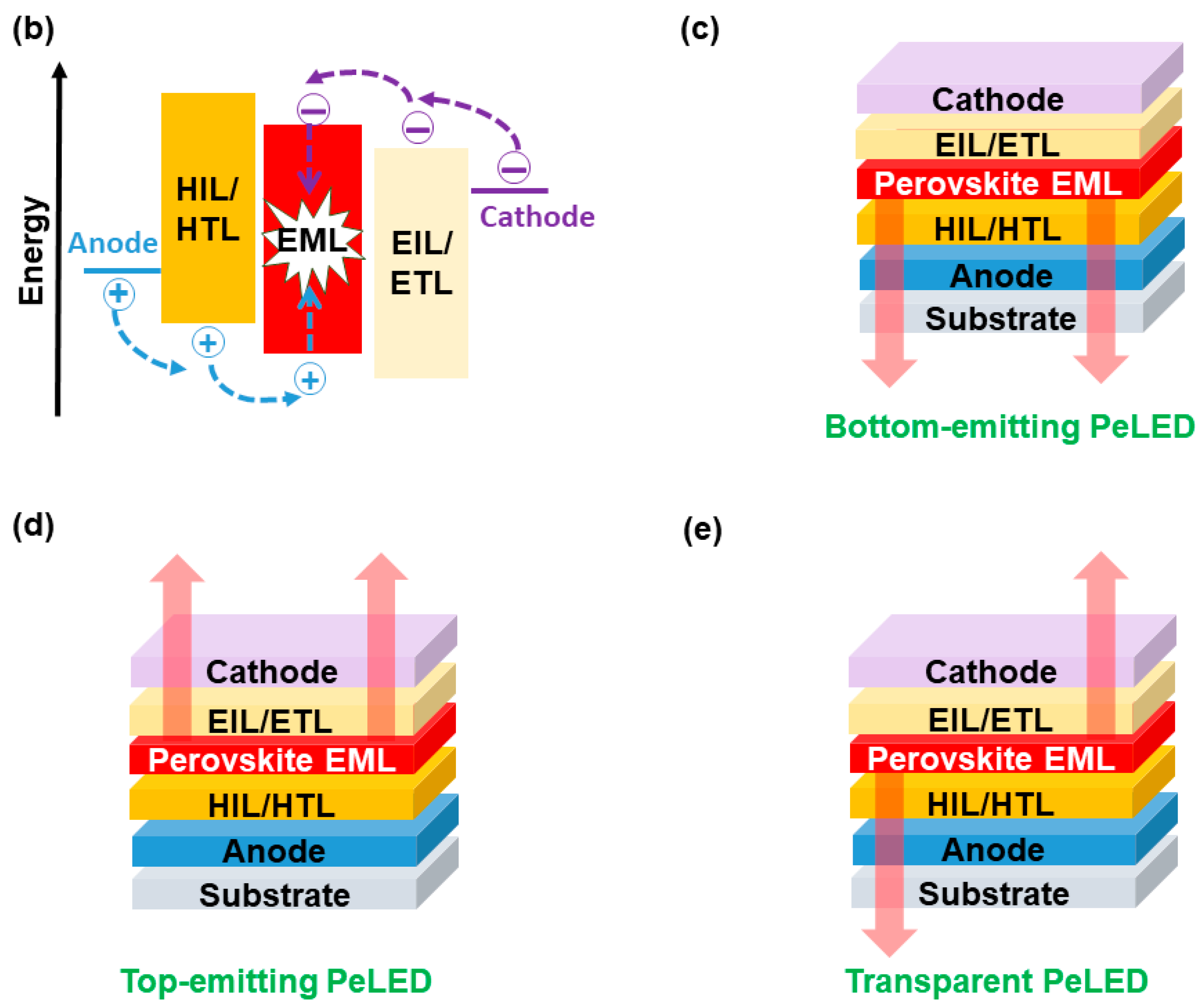
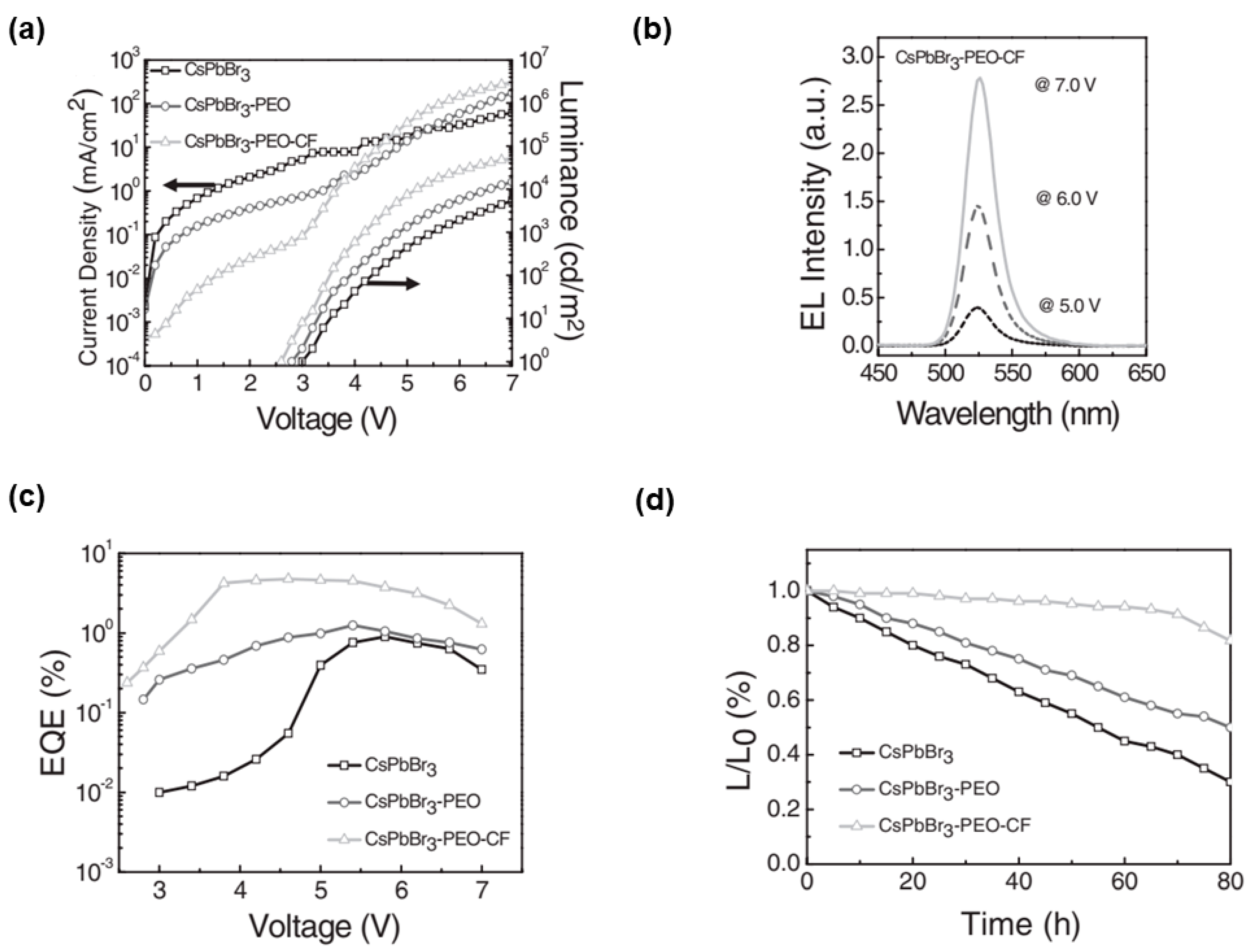
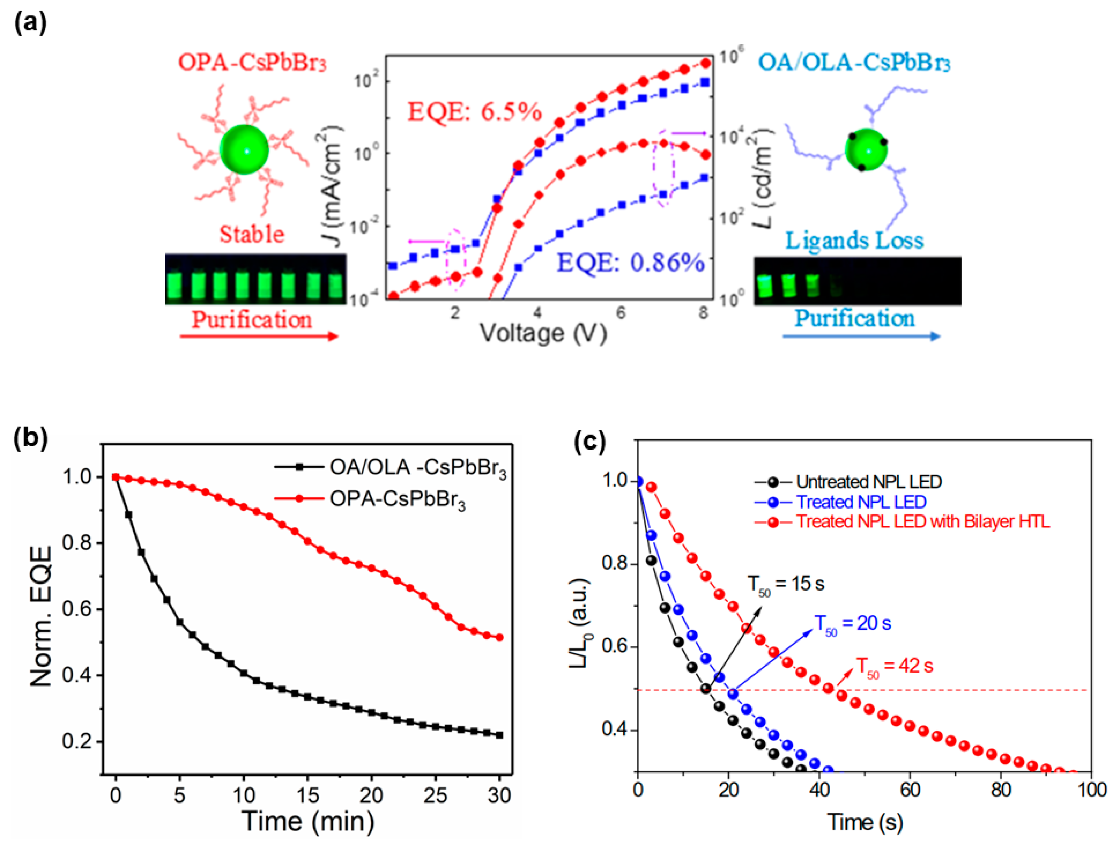
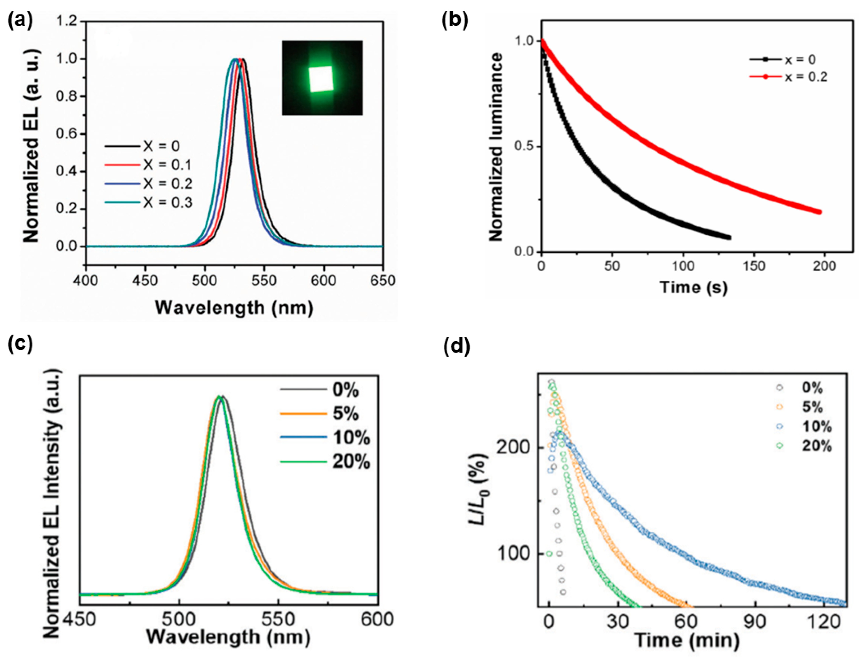
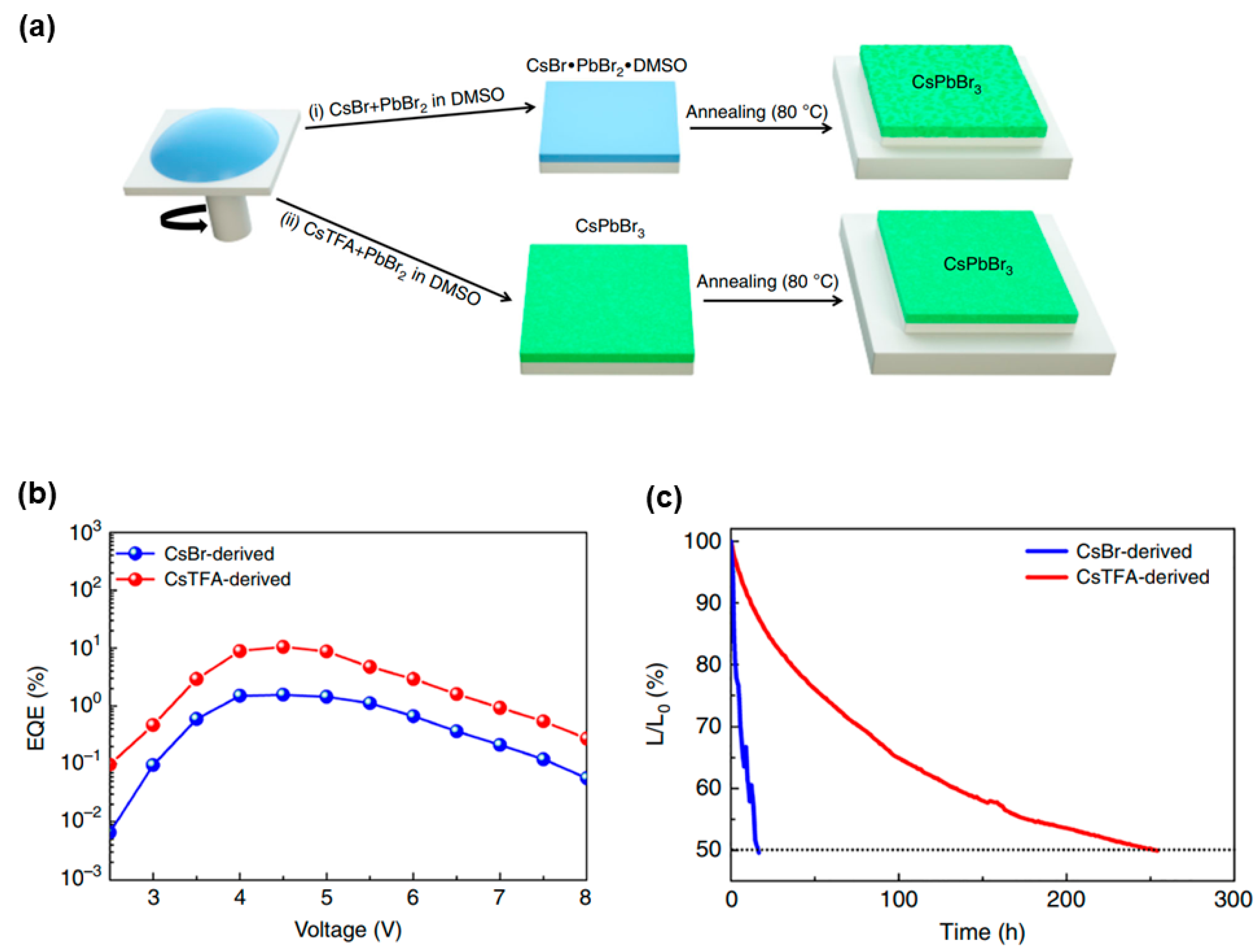
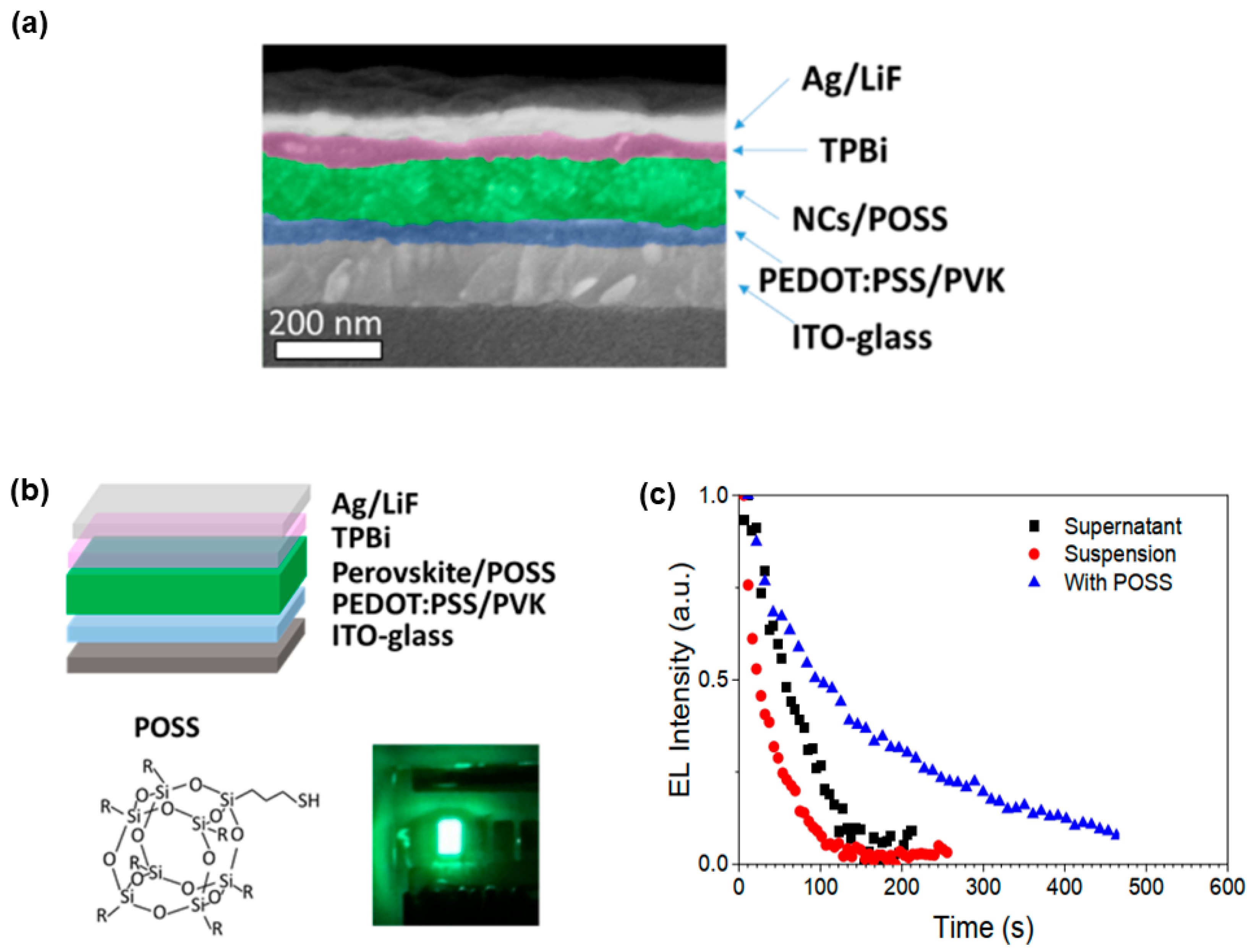
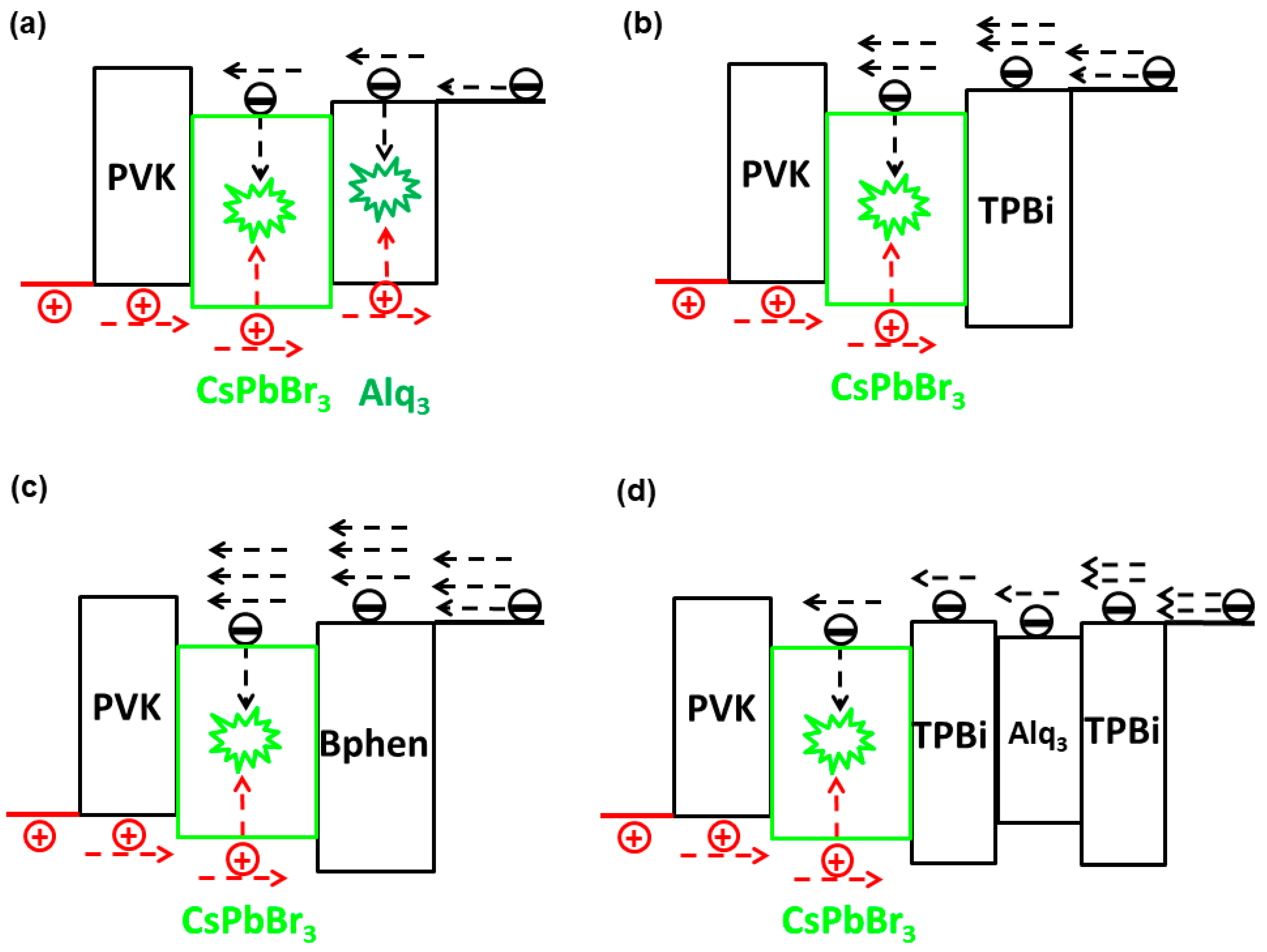
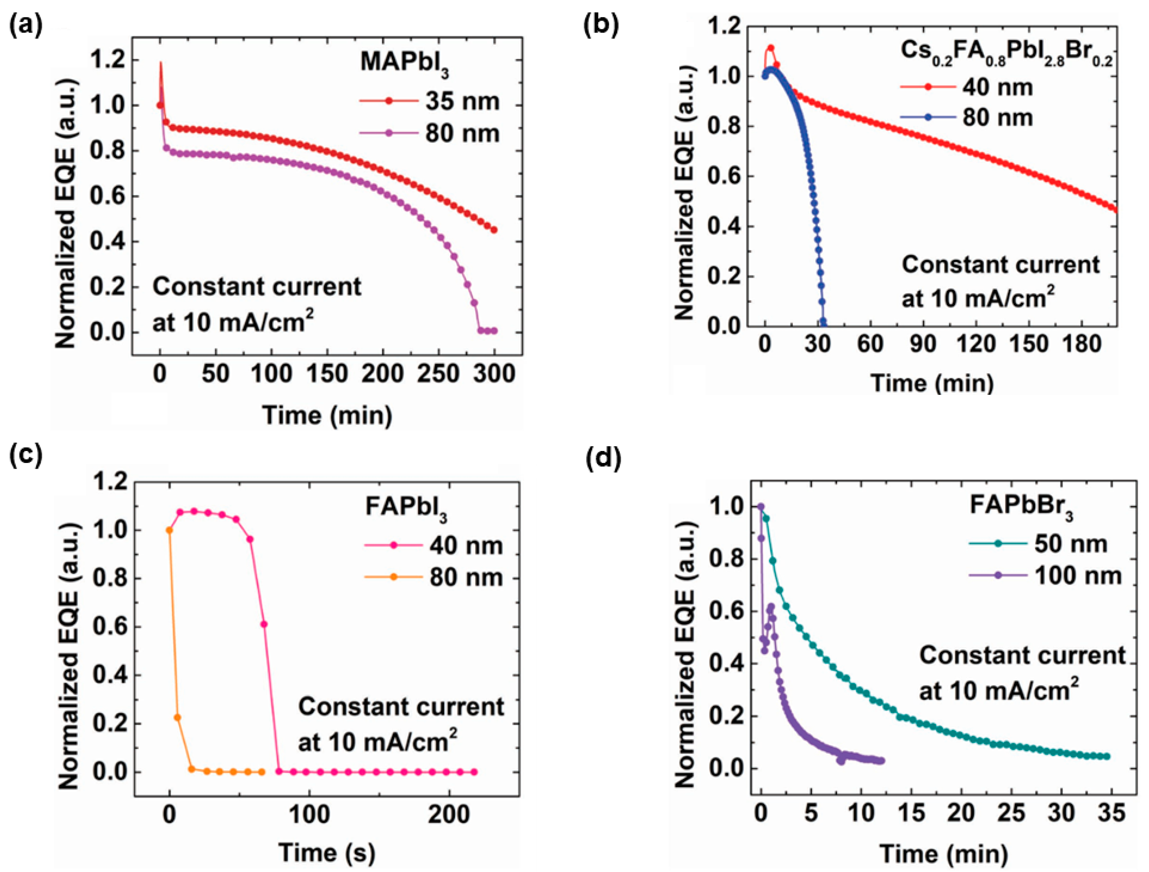
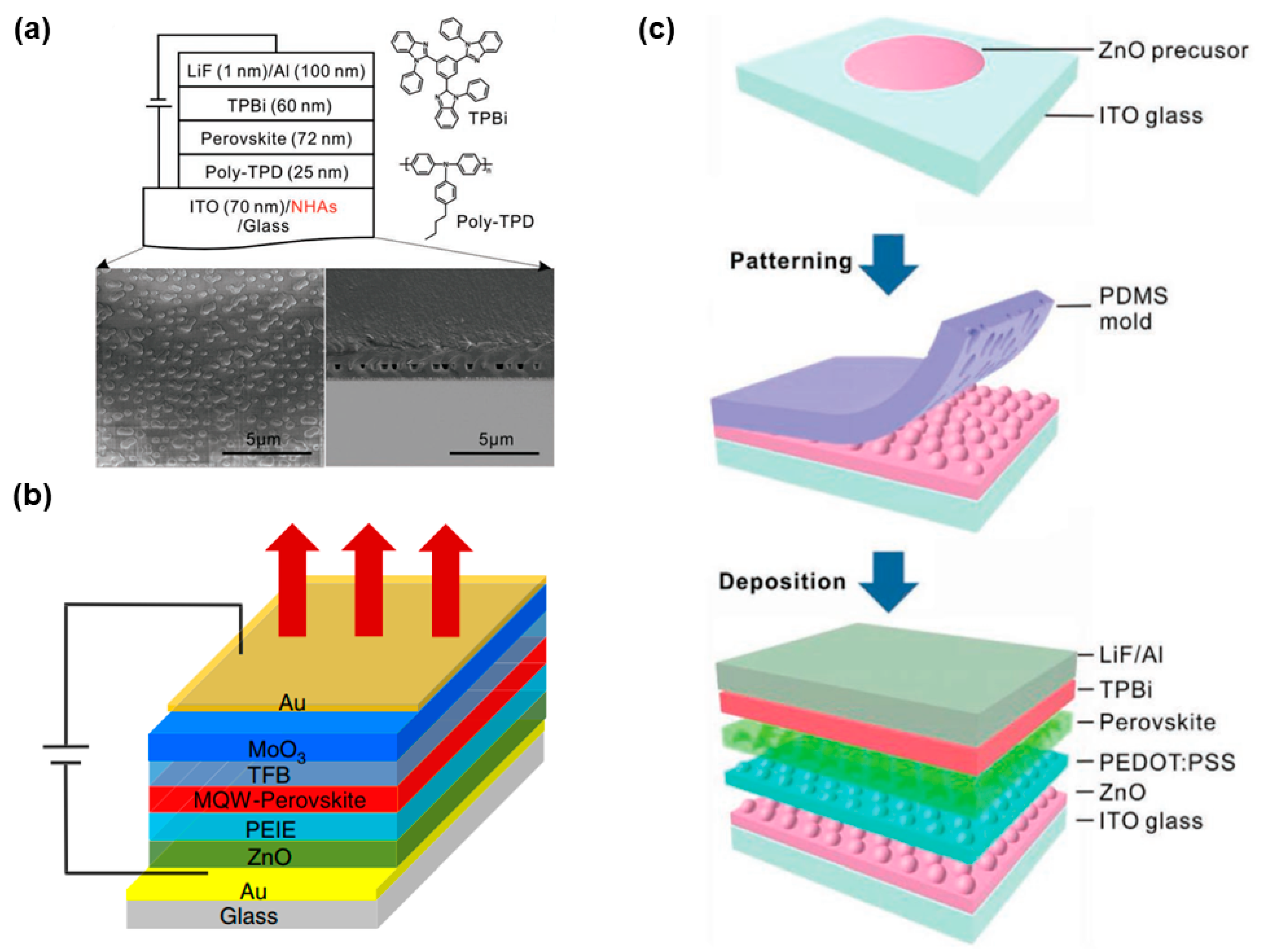
Table 1.
Summarized performances for representative PeLEDs possessing improved lifetime.
| Emitters a | Von b (V) | EQEmax c (%) | Lmax d (cd m−2) | Lifetime e | Reference |
|---|---|---|---|---|---|
| CsTFA-derived CsPbBr3 | 2.8 | 10.5 | 16,436 | T50 = 250 h at 100 cd m−2 | [28] |
| CsPbBr3-PEO-CF | 2.6 | 4.76 | 51,890 | 82% of the initial efficiency after 80 h | [124] |
| OPA-CsPbBr3 | 2.8 | 6.5 | 7085 | >50% of the initial efficiency after 30 min | [137] |
| DDAB-CsPbBr3 NPLs | 3.6 | 1.42 | 41.8 | T50 ≈ 42 s at 1 mA cm−2 | [138] |
| FA0.8Cs0.2PbBr3 | 3.5 | 2.8 | 55,005 | T50 ≈ 85 s | [158] |
| CsPb0.9Mg0.1Br3 | ~2.7 | 3.6 | 25,450 | T50 = 138 min at ~100 cd m−2 | [167] |
| CsPbBr3 | 5.8 | 0.35 | 2983 | T50 ≈ 120 s at 7 V | [193] |
| CsPbBr3 | 4.8 | 1.43 | 452 | T50 = 460 s at 9 V | [202] |
| CsPbBr3 | 3.0 | 2.39 | 3809 | ~80% of the initial efficiency after 10 h | [211] |
| FAPbBr3 | - | 11.3 | 79,700 | T50 ≈ 6 min at 10 mA cm−2 | [229] |
a The employed emitters in PeLEDs. b Turn-on voltage. c Maximum EQE. d Maximum luminance. e The lifetime of PeLEDs.
Publisher’s Note: MDPI stays neutral with regard to jurisdictional claims in published maps and institutional affiliations. |
© 2021 by the authors. Licensee MDPI, Basel, Switzerland. This article is an open access article distributed under the terms and conditions of the Creative Commons Attribution (CC BY) license (http://creativecommons.org/licenses/by/4.0/).
Share and Cite
MDPI and ACS Style
Xiao, P.; Yu, Y.; Cheng, J.; Chen, Y.; Yuan, S.; Chen, J.; Yuan, J.; Liu, B. Advances in Perovskite Light-Emitting Diodes Possessing Improved Lifetime. Nanomaterials 2021, 11, 103. https://doi.org/10.3390/nano11010103
AMA Style
Xiao P, Yu Y, Cheng J, Chen Y, Yuan S, Chen J, Yuan J, Liu B. Advances in Perovskite Light-Emitting Diodes Possessing Improved Lifetime. Nanomaterials. 2021; 11(1):103. https://doi.org/10.3390/nano11010103
Chicago/Turabian StyleXiao, Peng, Yicong Yu, Junyang Cheng, Yonglong Chen, Shengjin Yuan, Jianwen Chen, Jian Yuan, and Baiquan Liu. 2021. "Advances in Perovskite Light-Emitting Diodes Possessing Improved Lifetime" Nanomaterials 11, no. 1: 103. https://doi.org/10.3390/nano11010103
Note that from the first issue of 2016, this journal uses article numbers instead of page numbers. See further details here.