Frequency Selective Surfaces: A Review


1
School of Computer and Communication Engineering, University of Science and Technology Beijing, Beijing 100083, China
2
Beijing Engineering Research Center for Cyberspace Data Analysis and Applications, Beijing 100083, China
*
Author to whom correspondence should be addressed.
Appl. Sci. 2018, 8(9), 1689; https://doi.org/10.3390/app8091689
Submission received: 6 August 2018
/
Revised: 8 September 2018
/
Accepted: 10 September 2018
/
Published: 18 September 2018
Abstract
:The intent of this paper is to provide an overview of basic concepts, types, techniques, and experimental studies of the current state-of-the-art Frequency Selective Surfaces (FSSs). FSS is a periodic surface with identical two-dimensional arrays of elements arranged on a dielectric substrate. An incoming plane wave will either be transmitted (passband) or reflected back (stopband), completely or partially, depending on the nature of array element. This occurs when the frequency of electromagnetic (EM) wave matches with the resonant frequency of the FSS elements. Therefore, an FSS is capable of passing or blocking the EM waves of certain range of frequencies in the free space; consequently, identified as spatial filters. Nowadays, FSSs have been studied comprehensively and huge growth is perceived in the field of its designing and implementation for different practical applications at frequency ranges of microwave to optical. In this review article, we illustrate the recent researches on different categories of FSSs based on structure design, array element used, and applications. We also focus on theoretical breakthroughs with fabrication techniques, experimental verifications of design examples as well as prospects and challenges, especially in the microwave regime. We emphasize their significant performance parameters, particularly focusing on how advancement in this field could facilitate innovation in advanced electromagnetics.
1. Introduction
Metasurfaces are broadly named as planar metamaterials with subwavelength thickness and they can be easily fabricated while using lithography and nano-printing techniques. Both metamaterials and metasurfaces are rapidly growing research directions, and with their use, spatially varying EM or optical responses can be achieved at will, with scattering phase, amplitude, and polarization. Through a good selection of materials and design, the ultra-thin structure of MSs can considerably suppress the detrimental and undesirable losses in the wave propagation direction. When considering the polarization response, all metasurfaces can be categorized based on the operating principle of array element, i-e their functionalities (frequency selective surfaces (FSS), high impedance surfaces, perfect absorbers, reflecting surfaces, etc.).
According to the definition in [1], FSSs are metasurfaces that merely exhibit an electric response [2,3]. Since, in order to tailor the frequency selectiveness in transmission/reflection characteristics, only electrical polarization may be sufficient. From the theory of antenna and microwave engineering, these surfaces are made by planar and periodic arrays of metallic patches or strips with different shapes. The patch is of negligible thickness as compared to the wavelength, although it is larger enough in contrast to the metal’s skin depth. Consequently, such a structure can impeccably be estimated as a minuscule thin array of perfect conducting resonant elements. This approximation is also applicable to the complementary FSSs structures i-e apertures. However, aperture-type FSSs face a limitation when the area of the cavity/aperture becomes equal to the unit cell (a wire-mesh type) [2,3]. Square and hexagonal wire-mesh unit cells have typically been used and are also termed as the capacitive grid. The existence of the resonating size of array element causes the emergence of the side lobes in the transmitted and reflected fields, which are the defining feature of FSSs. However, as compared to the FSSs, the resonating element and unit cell of metasurface is relatively much smaller than the wavelength and it helps to eliminate the grating lobes in the frequency response. Therefore, FSSs in the terahertz domain are usually termed as metasurfaces [4].
Frequency selective surface (FSS) is a robustly studied topic of electromagnetic (EM) science, which are two-dimensional periodic structures having planar metallic array elements (patch or apertures) on a dielectric substrate, exhibiting transmission and reflection at certain resonant frequency [2]. Depending on the array element design, an incoming plane wave will be either transmitted or reflected, completely or partially. This happens when the frequency of the plane wave matches the resonance frequency of the FSS elements. Therefore, an FSS can pass or block the EM waves with certain frequencies in free space; so they are best identified as spatial filters.
Traditionally, the element size, shape, and periodicity of an FSS result in the resonance. FSSs have extensively been investigated over six decades and a range of microwave and optical FSSs structures have been evolved. In past, they were frequently used in reflector antennas [5], including diplexers for quasi-optical microwave devices, resonant beam splitters, and antenna radomes [6,7]. Nowadays, FSSs have been employed in dichroic sub-reflectors [8], radio frequency identification (RFID) [9], lenses antennas [10], and protection from electromagnetic interference [11]. Currently, the most famous applications of FSSs are as antennas radomes and controlling radar cross-section (RCS). Their performance is limited by the design complications, including the requirement of compact size and insensitivity to the incidence angle, as well as polarization of EM wave, consequently stipulating to improve their design features.
Traditional FSSs are narrow band and they do not provide adequate spatial filtering response. Extensive research is going on to miniaturize the FSSs and improve the frequency response with broader bandwidth (BW) at higher incidence angles and dual polarization. However, single layered FSS structures have been proved inefficient due to unstable performance with the variation of EM wave incident angle. To overcome the limitations of conventional single layer FSSs, multilayered FSSs have been introduced, which offer additional flexibility of varying parameters for desired performance [12,13,14,15,16,17]. At present, FSSs based on fractal elements and miniaturized arrays (2.5 dimensional) are employed for compactness [18,19,20]. Three-dimensional FSS structures and active FSSs have opened new doors in microwave technology [21,22,23,24]. Additionally, embedded FSS (with inserted metallic rods and plates based on stepped-impedance resonator) [25], integrated FSS and Electromagnetic band gap structures (EBG) [26], and metamaterial FSSs [27,28] are the most recent advances implemented by microwave researchers.
In the past, dispersion properties of FSSs have been explored through approximate analytical techniques, for example, which involve equivalent circuit method to analyze the transmission line characteristics (By Quasi-static approximation). However, with the growth of more complex structures, state-of-the-art numerical methods have been introduced, which use periodic boundary conditions (PBC) allowing for the design analysis quite straightforward. Some of these include finite element method (FEM), method of moments (MoM), finite difference time domain method (FDTD), and the integral equation (boundary element) method (IEM/BEM) [29,30,31,32,33,34,35]. A well-known technique is IEM/BEM used in combination with the MoM [36,37,38,39]. Various designs of FSSs and schemes to examine their EM characteristics are well presented in [2,3].
Regardless of its importance, a detailed review of the various types FSS is undeniably in its infancy. Particularly, an adequate demonstration of recent advancements in innovative FSS structures that are linked with their frequency responses is required. In fact, a detailed overview of different varieties of FSS from the standpoint of structure design, applications, and types of array elements, is yet to emerge in the literature. Although a few review articles are available on FSSs or FSS based EM structures in broad frequency regimes [4,22,37,40,41,42], however, in this article we specifically discuss the different kinds of FSSs operating at wavelengths in microwave range. Figure 1 depicts a comparison of presented review with already available survey articles on FSSs. A more detailed assessment of existing surveys in the literature is outlined in Table 1.
As shown in Figure 1, the category 1 details theoretical reviews; for example, which discusses a number of techniques to analyze FSSs as filters in the microwaves and optical ranges, and circuit analytical review to underline the range validity of some model with their accuracies. In category 2, while there exist some survey articles that target architectures of particular types of FSS, more focus has been set in the literature toward the specific FSSs types (including metamaterials or metasurfaces FSSs), FSS based antennas, and other FSS based EM structures.
On the other hand, researchers have less considered the survey on the different types of FSSs that have recently evolved based on structural design, applications, and nature of array element used and have taken this lack as for granted. Therefore, in this review paper, we provide an outlook of skyrocketing research field of FSSs by assessing the progress during the past years primarily focusing on categorizing the FSSs as mentioned above. The contributions of our effort in this review paper are as follows.
- (1)
- Through a careful study of the existing surveys on the FSSs, we identify the survey gap in the existing reports, as briefed in Table 1, which accentuates the requirement to report most up-to-date FSS types, especially in the microwave regime.
- (2)
- Next, we present a classification of the FSSs, focus on the importance of their functionalities, and categorize FSS on the basis of nature of array element used, structure design, and applications.
- (3)
- This paper targets to link among their crucial theoretical, structure geometry, and significant performance parameters.
- (4)
- For every functionality, the polarization state of the array elements and the physical mechanism of their functions must be related to the frequency responses provided by FSSs. By knowing the polarization characteristics of FSS periodic elements for a specific function, the implementation of required FSS response in certain frequency band becomes straightforward and therefore, we elaborate all types of FSS from this perspective.
- (5)
- We illustrate an extensive survey of most recent researches on FSSs and also include their fabrication techniques, experimental verifications of FSSs design. Prospects and challenges, particularly in the microwave regime, are discussed focusing on how the innovation in this field could smooth the progress in advanced electromagnetics. The article is organized, as described below. In Section 2, we overview the concept of periodic surfaces with some of their types. In Section 3, we introduce FSSs in detail and its theoretical background, along with some history and significant advances in recent years. In Section 4, we review different types of FSSs, their related properties, implementation, and fabrication techniques. Section 5 presents future challenges, trends, and potential applications of FSSs. In the last section, we provide concluding remarks and a point of view about future research directions.
2. Periodic Structures
When identical elements are arranged in an infinite array of one or two-dimensions, a periodic surface is formed [2]. Two basic means to excite a periodic array are known: one is through an incident plane wave (a passive array type) or by the attached generators to individual element (an active array type). In the former type, the incoming plane wave (Ei) will partially be transmitted (Et) in the forward direction and in part reflects (Er) specularly. In the condition of resonance and without grating lobes, the amplitude of the reflected wave Er may be equal to incident wave Ei, while the transmitted signal Et is equal to zero. The specular reflection coefficient (Γ) can be defined by (1).
Similarly, the transmission coefficient (T) can be defined by (2).
In the active array type, the voltage generators must possess the same amplitude and also a linear variation of the phase across whole active array elements so that it may be regarded as a periodic surface [2]. Dipole and slot arrays with a similar shape of elements constitute complementary arrays so that when both of these arrays are positioned on top of one another (cascaded), a perfect conducting plane is created. The transmission coefficient of one array is equal to the specular reflection coefficient of its complementary array and is simply termed as Babinet’s principle. In order to obtain a stable resonance with variation in the angle of incidence for a periodic surface, the inter-element spacing must be kept very small (<0.4λ) [2].
High impedance surfaces (HISs) [45] are electrically smart, two-dimensional arrays that are designed to totally reflect an in phase incoming plane wave and reject bounded surface waves. They can be employed to suppress propagation of surface modes. EBG possess such characteristics and similar type of structures, named photonic band gap structures (PBG), explain an impulsive and forbidden emission. Perfect conducting surfaces (PCSs) create destructive interference when excited by antennas, horizontally polarized and closely-spaced. Conversely, perfect magnetic conductors (PMC) provide constructive interference due to magnetically induced surface currents. PMCs are naturally non-existent, however; artificial magnetic conductors (AMCs) are artificially produced PMCs, and from EM perspective, these are dual to PCSs. AMCs are based on periodically engineered structures that act as a sheet of magnetic currents having magnetic polarisability.
FSSs are usually designed by periodic metallic arrays of elements on a dielectric substrate and exhibit transmission and reflection characteristics at a certain resonant frequency. Mushroom structures are the class of FSSs that is designed to resonate at low frequencies as the distance between metal array element and a metal plane creates an inductive effect at microwave regime. Similarly, perfect absorbing surfaces are thin layer structures which absorb nearly all the incident power of EM wave at a particular frequency and angle of incidence at microwave to optical operating frequency ranges. In conclusion, it is worth mentioning that if the periodicity of the array elements (Inter-element spacing) is not very small when compared to the wavelength in free space, it may not be possible for periodic structures to reach a stable resonance with varying angles of incidence [2].
3. Frequency Selective Surfaces (FSSs)
At microwave and optical frequency ranges, spatial filtering is the most desirable operation in all signal processing systems. Frequency selective surfaces (FSS), also called spatial filters, are used to modify the EM wave incident on such surfaces and provide dispersive transmitted and/or reflected characteristics. FSSs are usually designed by periodic metallic arrays of elements on a dielectric substrate. The change brought to the transmitted wave can be both in amplitude or phase when compared to the incident wave. In any case, selectivity may be introduced against the incident polarization to improve the irregularities in the emission pattern, which is exhibited through a change of the phase or amplitude of the transmitted wave. A variety of applications according to different requirements can be facilitated, depending on the nature of modification added to the transmitted wave.
Low profile, reduced periodicity, dual polarization, angular stability, multi-pole frequency response with higher out-of-band rejections, and easy manufacturability are some of the desired properties of FSSs. Nevertheless, achieving all the aforementioned characteristics for an optimized design has been a challenge for the FSSs designers [2]. Different techniques to dig out best EM properties utilize various element shapes and varying geometric design parameters, such as adjusting the structure element size (patch or aperture), dielectric substrate, and tuning the inter-element spacing [2,46,47]. In this paper, we present different varieties of FSS structures that are used for specific EM applications. Additionally, approaches for implementation, fabrication, and testing of these structures are also studied.
3.1. Operating Theory of FSS
FSS structures (capacitive and inductive), also called spatial filters, are analogous to the microwave filters according to the circuit theory. Filtering characteristics of FSS can be categorized into the four kinds, including low pass, high pass, stop band, and passband. Low pass FSS filters permit a lower range of frequencies to pass through the structure, while bypass higher range of frequencies. High pass FSS filter operation is a counterpart of low pass filter function by applying Babinet principle. Similarly, stopband FSS filter blocks undesired frequencies while passband FSS filter allows only specific frequency range. For a desired resonant operation, FSSs are designed by periodic arrays of metal patches and/or slots etched on a dielectric material. The appropriate selection of FSSs array elements, shape, dimension, and substrate material is the most important part of the design process.
The operational theory of FSS based structures has been explained by Munk in detail [2]. Figure 2 shows the functionality of FSS achieved by a complementary self-resonating network. Simply, when EM waves are incident on FSS structure, they incite electric currents into the array elements. The level of coupling energy defines the amplitude of the produced currents. However, these generated currents also work as EM sources and they create additional scattered fields. Incident EM fields combined with these scattered fields make up the resultant field in the surrounding of FSS. Consequently, the required currents and field characteristics can be obtained by properly designed elements and create the filter response.
The patch elements (dipole FSSs) are designed to act as stopband filters for incoming plane waves and work as completely reflecting surfaces in a narrow band of frequencies. Their counterparts, the aperture elements (slot FSSs), demonstrate passband characteristics, means that they behave as transparent surfaces to incident EM waves within the working band of frequencies. Nevertheless, to accomplish the functional necessities for a variety of EM applications, conventional FSSs come across a limited use due to their inadequate filter response, low angular stability, and narrow bandwidth.
Figure 3a shows two basic types of element, equivalent circuits, and filters responses for low and high pass FSSs [2]. FSS patches create resistance (R) and inductance (L), while gaps among the FSS elements generate capacitance (C). Simple electrostatic principle applies to manipulate the physical significance of these passive values for different FSS elements, e.g., L of two parallel wires and C generated by a parallel plate capacitor. So, a required filter response is constructed by the combination of these capacitive and inductive elements. However, any change in the FSS dimensional parameters leads to an equivalent variation in the L and C values. Physically, when a unit cell of an FSS is illuminated by the EM wave, it can be converted to an equivalent resonance circuit. The resonance frequency can be found by (3), in which L and C represent the equivalent inductance and the capacitance of an FSS unit cell, respectively.
Choosing an appropriate array element is very crucial in designing FSS. While various unit cell geometries have been implemented, out of which some are easily controllable and so more famous in FSS community. A classification of frequently used FSS elements types is summarized in [4] based on their resonant properties. For example, non–resonant element (patch, wire grid) can be modeled by a capacitance, whereas single resonant element (like loop, cross, dipole) can be represented by a series combination of capacitor and inductor. It is to note that the number of resonances has a direct relationship with the count of lumped elements.
3.2. Principle of Periodic Structures (e.g., FSS)
Principally, there are two ways to find the impedance and scattering properties of periodic structures [2], first is mutual impedance method which is linked to MoM and second is the plane wave expansion approach, also called the spectral method. Periodic FSS structure can be designed based on Floquet theorem. By definition, a periodic structure must be infinite in extent. A planar array which is infinite in x- and z-direction with identical inter-element spacing (Dx = Dz) is termed as a truly periodic configuration (infinite × infinite) and is shown in Figure 3b. Assume if the array is incident by an incoming EM wave propagating in certain ŝ direction is given in (4).
The amplitude of currents on the entire element will be equal, while the phase of the incident EM field will match with the phases of these currents. By Floquet’s theorem, the element currents in column m and row n are given as (5) [31].
Using Ohm’s law for reference element 0, 0 gives (6).
and, array scan impedance is given by (7).
3.3. History and Significant Advances of FSS in Recent Years
FSSs have extensively been explored over the past five decades [2,3] and the evolution process extends from simple geometries to the complex designs. Strict requirements of performance in advanced applications have stimulated considerable advancements in analytical techniques, computational power management, and manufacturing technology. Huge potential for military use has lead to intensive studies of such surfaces since mid-1960s. Although on record, the oldest patent came in 1919 to the well-known Marconi and Franklin. The earlier FSSs research focused on developing Cassegrain sub reflectors used in the parabolic antennas. During the Persian Gulf War, the Lockheed F-117 Nighthawk was openly launched by US air force, which increased the significance of stealth technology and FSSs. Although the adjustment of radar cross section is considered as the most thrilling function of this technology, FSS are employed in many other useful applications. These include dichroic sub-reflectors, radomes, RFIDs, lenses, and electromagnetic interference (EMI) protection.
Mode matching methods were initially applied in waveguide problems for the behavior analysis of FSS, which gave rise to approach for equivalent circuit modeling [43]. This was partially based on the transmission line theory. However, it had a limited analysis capability to model the FSS geometry. More precise numerical techniques have been developed with the introduction of fast processing computers e.g., MoM, FEM, FDTD, and IEM/BEM. Verification process has now replaced the bolometer used in earlier experiments with modern Vector Network Analyzers with high capabilities of measurements for amplitude and phase of the scattered EM fields. Fabrication ease and cost effectiveness are essential factors that are investigated so far, since the precision in etching defines the performance of an FSS and it is usually required to be achieved over vast areas of such surface.
Starting with a simple FSS or multiple cascaded FSS realizing a band-pass or band-stop characteristic, the slot and patch elements are complementary and are linked by Babinet principle. Generally, FSS applications presume those geometries which are periodic and represented by a unit cell repeating itself indefinitely [2]. However, several practical applications of non-periodicity exist, for example, in the use of curved surfaces, and infinite smooth surfaces, which may have randomness in geometry and its constituent properties [43]. Moreover, the selection of direction-dependent screening has been achieved by non-reciprocal FSS structures. Some initial uses of FSS lie in the design of radomes and sub-reflectors for reflector antennas and still extensively studied. Capabilities of functioning at lower frequencies and broader bandwidth have been facilitated by the lightweight, conductor-backed thin radar absorbing FSSs.
Furthermore, since the “metamaterial” term was coined, there has been a stirring revitalization of interest in metamaterial EM structures, especially metamaterial inspired FSSs are investigated for compact filters, absorbers, and sensing applications. Recently, periodic structures having three-dimensional (3D) elements is being used with great interest as they allow the electric currents to flow with components at right angles to the surface and therefore, FSS geometries insensitive to the incidence angles may be designed [43]. Complex FSS structures are manufactured with advanced fabrication techniques by joining together consecutive layers of different shapes, such as tetrahedral Calthrop, is fabricated with a printer employing the fabrication process of fuse-filament.
With the increase in satellite communication and pulse-powered devices, metallic FSSs have been proved incapable to operate the power/heat produced by such systems efficiently. In such applications, enhanced field, heat generated by Ohmic-losses, and dangerous emission of electrons, are exceedingly frequent problems that result in the flashover and electric discharge. Quite recently, a miniature element FSS has been encapsulated in a dielectric by means of a high break-down power to minimize the amplitude of the electric field [48]. Peak power of about 25 kW could be handled with this method. From the above illustration, it is evident that FSS is a massively growing area and needs more state-of-the-art methodologies and innovative research to support foreseen novel applications of FSSs.
4. Types of FSSs
Here, in this section, we categorize the FSSs on the basis of array element, structure design, and application. Figure 4 gives the taxonomy of the FSS presented in this article.
4.1. FSS Based on Array Elements
In this review article, we cover three types of FSSs based on array elements, including basic element type FSSs, convoluted/meandered FSSs, and fractal FSSs.
4.1.1. Basic Element Type FSSs
In general, four basic types of FSS element groups have been classified [2] and are illustrated in Figure 5. This includes Group-1 (centrally connected or N-poles, such as dipole, tripole, square-spiral, Jerusalem crosses), Group-2 (looped shapes, e.g., circular, square, hexagonal loops), Group-3 (solid interiors or patch shapes of different shapes), and Group-4 (combinations of above all). Depending on the potential application, FSS designers select array element from any of these groups and/or use a combination of these as well. A good element should present a stable resonance response with the variation in incidence angles. Commonly, selecting a group-2 element with a larger loop area is beneficial and it enhances the bandwidth [2].
Simple circular loops, square loops to advance loaded elements with three or four legs have been utilized; especially hexagonal loop structures are useful for wideband applications. When circumference (perimeter) of the loop element becomes equal to a full wavelength, FSS reaches the resonance. It is found that an ample range of bandwidth can be achieved by changing the shape of these loop elements i-e loaded three or four-legged elements, which are narrow band, whereas hexagon loops are ultra wideband.
Nevertheless, the bandwidth of almost all types of FSSs can be varied by altering the inter-element spacing, which must be small in terms of the wavelength. If the inter-element spacing is greater than half of the wavelength, it will result in the early onset of the grating lobes, pushing the main resonance towards downside with varying incidence angles.
Depending on the effective permittivity and with convincingly large inter-element spacing, such FSS resonates when the circumference is equal to a wavelength [2]. The bandwidth increases when the inter-element spacing is reduced. On the other hand, at a certain closer distance, this increases the inter-element capacitance as well, thereby pushing the resonant frequency towards the lower side. To overcome this discrepancy and regain the desired resonant frequency, the circumference of an element should be reduced. Group-1 stands next to loop family. With proper design of elements in this group, inter-element spacing can be reasonably reduced to experience extremely large bandwidth, for example, in case of gangbuster elements. This way, the inception of grating lobes is significantly delayed. Group 3 consisting of solid interior elements are mostly used in combination with complementary elements that are adjacent to it.
Conventionally, the general attribute of FSSs is that they reach resonance at the desired frequency only when the patch or slot size in the unit cell becomes at least in the order of half of the wavelength. However, this limitation can be overcome by minimizing the electrical dimensions of the constituting element/inclusions at subwavelength level to ensure insensitivity to variations of incident angle and polarization. To facilitate such a requirement, FSS with miniaturized element is proposed by Sarabandi et al. [49], in which small metallic arrays are periodically printed in patch layer (capacitive mesh) on one side of a dielectric substrate. Wire grid patterns (inductive mesh) with equal subwavelength periodicity are arranged on the other side. Both capacitive and inductive layer in combination with the dielectric substrate, produce a parallel resonating LC-circuit. With such a structure arrangement, it is possible to organize a higher quantity of unit cells in a compact space [12], which is of practical importance for some sensitive low-spaced applications, like radomes. It is noted that an arbitrary phase front can efficiently be achieved for miniaturized unit cells, which can reduce the angular sensitivity of the incident plane wave. However, the double or multilayer FSS structures face errors resulting from fabrication process, sensitivity in response, and also a substantial amount of insertion loss at the resonance arising from strong effects of the localized electric field within the lossy dielectric medium. Table 2 presents different types of FSS structures utilizing some basic type and advanced elements showing their nature of filter and number of layers.
4.1.2. Convoluted or Meandered FSSs
Some applications demand miniaturized FSS, especially in radomes where flexibility is a challenge for FSS designers. FSSs with relatively small electrical dimensions are enviable, so that the unit cell size is reduced without affecting the angular stability. It is proved in [50] that the convoluted square loop FSS structures can present better stability in polarization as compared to the simple element.
Furthermore, in [62], it was studied that smaller unit cells are less distorted for a specified amount of curvature. Through convolution square loop, the element area can be minimized by a significant factor that may exceed an order of magnitude. The concept of convoluting the elements to reduce the unit size is a constructive approach to tighten the curved structures and evidently isolate the grating lobes effect from the fundamental resonance. However, manufacturing limitation falls on the way as a penalty to pack the resonating length to diminish the unit cell of a particular area.
Miniaturized FSS with convoluted square loop array elements was initially coined in [62], and Figure 6a shows such a structure shape [50]. This FSS provides effective shielding in X-band with 3dB fractional bandwidth (FBW) of approximately 48% enough to cover this band [50]. Miniaturized array elements with interwoven geometry, as shown in Figure 6b, have efficiently been used to provide selective frequency isolation in office windows and thus signal-to-noise ratio is improved, delivering great advancement in the reliability of mobile communications [63]. Similarly, to address the challenge of minimizing the unit cell, meandered elements are introduced in [64] to increase the resonant lengths, in which four symmetrical and spiral shapes of metallic FSS element are printed on one side of a dielectric substrate, as shown in Figure 6c. It is observed that these meandered lines are different from previous works as in this research; the element slots are nested with their neighborhood. The length span of resulting cross spiral slot is long enough to efficiently increase the equivalent inductance as well as the capacitance at the same time, allowing for this compact arrangement to demonstrate promising stability under oblique incident angles and polarizations.
A similar concept of meandered lines was studied in [65,66]. The conception of meandered array element not only trims down the unit cell size, but also gives a stable stopband frequency response (in case of loop type FSS) for higher oblique angles of incidence, and segregates the main resonant frequency from the grating lobes. With the inclusion of meander lines, small partitions exit between the wire elements and hence the capacitance produced between them having effectively reduces the resonant frequency, as shown by the graph in Figure 6d [66]. Further, it is deduced that considerable bandwidth variation is attained by cascading two FSS arrays with air-gap separation (2–80 mm), as shown in Figure 6e. Cascading of FSSs produces a cyclic effect in the bandwidth with the change of the thickness and it also may be due to the standing waves that were created by the EM fields in the partition region that couple the power from one FSS layer to the next.
Although FSSs that are designed by using space-filling curves possess simple geometry, which is an attractive choice for smart applications requiring higher stability in dual/multi band performance. The reduced independent controllability, high insertion loss, and fabrication/implementation difficulties are some of the problems faced in miniaturized dual-band single screen FSSs. Comparatively, FSS in [67] is made up of crossed-dipole aperture element united with meandered mono-pole symmetrical aperture element, as shown in Figure 6f, and provides passband responses at C and X bands. It is noticed that two pass bands are adjustable independently, simply by changing the geometric parameters of the elements while offering wider bandwidth and lower insertion loss. It is observed that the cross-dipole element largely controls the first resonating frequency, whereas the second resonant frequency is primarily determined by the meandered mono-pole element.
4.1.3. Fractal Based FSSs
Nowadays, significant research in microwave engineering is reported in the design and development of new FSS designs based on the theory of fractal geometry due to its attractive features [29,68]. Geometric patterns generate fractals through an iterative procedure for an infinite number of times [69]. However, pre-fractal shapes originate by truncating the iterative method after a finite number of iterations. FSS with fractal elements was originally proposed in [62] to cut down the size of the structure by applying the space-filling curves of Hilbert and Minkowski. Later, the innovation in recently reported researches has brought unprecedented prospects for engineers to investigate unlimited possible fractal configurations that had not existed in earlier time. Important performance attributes that are realized by fractal arrays include efficient methodologies to element size reduction, multi-band behavior, low-side lobe designs, and improvement in fast beam forming algorithms by utilizing the recursive property of the fractals [70,71].
Fractal FSSs are famous for their self-similarity nature, thereby creating multi-band response and compactness. The multi-band frequency response of Sierpinski fractals has lucratively been used in the past for designing dual-band FSSs [72,73]. Additionally, the impact on the frequency response has been investigated via the scaling factor, iteration level, and width of the metallic patch [29,74,75]. It is proved with the increase in the electrical length of the fractal patch, a decrease of the working frequency is achieved, and for that reason, a lessening in the structural dimensions is observed. Figure 7a–h gives an overview of some of the fractal shapes used in recent researches.
Fractals occupy a much smaller area because of their efficient space usage. The Koch dipole (Koch curve family) is much smaller than a straight wire dipole whereas both of them resonate at the same frequency. A Koch curve is generated by an iterative process, as shown in Figure 8a [76]. The whole length of a Koch curve at its Nth iteration is (4/3)N of the length at zeroth iteration (a straight line). Therefore, a Koch dipole starting and ending at the same point as its normal dipole counterpart effectively offers a much greater length and thus a lower resonance frequency. In fact, this results in a miniaturized element design.
(1) Fractal Dimension and its Generation by Iterated Function System
To obtain self-similar dimension, the fractal geometry is divided by scaling it down with replicas of itself. If the scaling fraction is “sf” and “N” copies of the original geometry to be made, and then the self-similarity dimension (SFD) is defined in (8) [76].
As an example, four copies of a fractal square can be made with sf = 1/2, nine copies with sf = 1/3, 16 copies sf = 1/4, or N2 copies of sf = 1/N. Using above formula, the SFD is established to be equal to 2. SFD of several fractal geometries can be determined with this approach. A wide range of practical fractal element structures can be generated while using an extremely adaptable method called Iterated Function System (IFS) [71]. IFS is an effective design tool in fractal antenna engineering and fundamentally offers a generic structure for the characterizing and manipulating the fractals.
(2) Research on Fractal FSS
Fractal FSS surfaces design based on the Minkowski islands, inset crossed dipole periodic cells, and Sierpinski carpet fractals were investigated in [29]. The simulation methods incorporating periodic boundary conditions allow for periodic arrays of complex elements to be analyzed. These include periodic MoM, which gives liberty to simulate tilted FSS surfaces for varying incidence angles and periodic finite difference time domain (FDTD) technique by which complex periodic arrays elements can efficiently be simulated. It is observed that the two later kinds of fractals provide multiband responses with a superior relationship between the structure geometry and the prediction of stop bands, while former fractal gives most closely spaced resonances. Conversely, transmission in the passband between the two stop bands is relatively lossy which can be made constructive for some applications. Importantly, a number of bands with the desired bandwidth are possible, and the passband performance can be improved by making a trade off among geometric shape, periodicity, and supporting dielectrics substrate.
An interesting property of fractals is the opportunity of acquiring arbitrarily longer curvature confined in a specified area/volume. This characteristic has been effectively utilized in reducing the inter-element spacing between the resonating shapes of FSS. The fascinating feature of “self-similarity” facilitates to realize a multiband performance. However, a truly multiband FSS design encounters a major limitation, i.e., appearance of grating lobes, which can be overcome by minimizing the spacing between neighboring elements as compared to the free space wavelength. On the other hand, the inter-elements spacing cannot be smaller than their length. The Sierpinski dipole exhibits a multiband response that is known after the invention of Sierpinski gaskets or Sierpinski triangles [69]. Earlier, it is proved by Romeu et al. that Sierpinski fractal FSS without dielectric substrate can merely show dual band behavior [77]. This is to note that in Sierpinski gasket, a scale ratio exists between a triangle and the triangles built in the subsequent iterations of one half.
The Sierpinski dipole shape gives enough freedom to modify its geometry and tune frequency response [73]. It is recognized in this research that the resonant frequencies are related to the span length of the dipole edge (2*h) instead of its height. As a result, the resonant frequency becomes low at a certain height when the flare angle of dipoles is widened, as seen in the trend graph of Figure 8b. Additionally, the distance between the first and the second resonance roughly remains the same with the variation of flare angle. It has been examined that by suitably perturbing the shape i-e the scale factor, the ratio between resonant frequencies can be modified. Trends of the resonant frequency in Figure 8c shows the effect of different scale factors, and it can be inferred that it is possible to adjust the frequency response to a definite extent for a Sierpinski dipole FSS.
Gosper hexagonal and Dürer pentagon patch fractals were proposed in designing of compact FSS based filters in [78,79]. Stopband filtering with dual-band responses and broad bandwidth is exhibited by these spatial structures. Their EM performance parameters (resonant frequency and bandwidth) can be adjusted without modifying their original size. The tuning at the required frequencies range is possible because resonant frequency decreases by increasing the number of fractal iterations. Also, with an increase in the periodicity of the structure, the resonant frequency is lowered while narrowing the bandwidth. Nonetheless, a reduced effect is pronounced when the fractal iteration is increased. Metallic Koch fractal with two-dimensional periodic array elements is reported in [80] for miniaturization of FSS. Recently, fractals have been used to design compact and angularly stable FSSs [81].
Promising and desirable FSS performance characteristics with Peano pre-fractals is claimed in [82], for instance, adjustable transmission features, compact designs, higher frequency compression factor, stable frequency responses for oblique angles of incidence wave, and multiband behavior. Any fractal geometry whose fractal dimension (SFD) is equal to 2 is named as Peano curve [68]. Originally, Peano curve consists of a base-motif fractal, which makes use of a line segment for its base. Figure 9a shows Peano fractals (k = 1 and k = 2) with an octagonal base of metallic patches printed on a single layer of fiber glass has been used for reconfiguration which is an attractive feature for some antenna systems and transmission management in buildings requiring wireless applications [82]. The possibility of FSS reconfiguration is facilitated by assuming particular switches to be turned off (S1–S8).
As seen in Figure 9b, with the increase of iteration level, the number of resonances increases from 3 to 7. Analysis of increasing the inter-element spacing shows that for k = 0, the resonance frequency lessens and the BW narrows down, as depicted in Figure 9c. However, for k = 1 and k = 2, a slight increase in resonant frequency is examined. Figure 9d gives the trend graph of varying angle of incidence and shows stability for fractal level 1 and 2, while deviations of 33% and 0.49% in resonance frequencies are found for k = 0 and k = 2, respectively. Similarly, an increase in BW is seen for higher oblique angles with level 1 and 2 as compared to level 0 and tendency is shown in Figure 9e. Such flexible fractal patch element can provide many combinations of reconfigurations, though the drawback is that a reconfigured patch loses its symmetry and hence dual polarisability.
Fractal elements can also be employed in designing FSSs for wireless security and mobile communication especially to protect security staff in buildings against harmful EM radiation in L or S-band. In this band of frequencies, FSS proposed in [81] demonstrates good reflection characteristic to screen out the EM energy; while at 900/1800/1900 MHz and 5.2/5.8 GHz, this fractal structure works as a good transmitter (a passband filter). The design made by regular hexagonal patches and equilateral triangle shaped array while using a fractal structure can efficiently reduce the unit size and maintains the stopband characteristic of this ring shaped FSS. Through proper symmetric configuration and a small gap between the two adjacent cells, the resonance frequency can be diminished by using high permittivity material, as revealed in Figure 9f. With resonance frequency in vacuum f0 and relative permittivity ϵr, the resonance frequency fr can be calculated by (9).
Desired resonance frequency in reject-band can conveniently be gained by using the certain dielectric material, for screening out the WiMax, WLAN, mobile communication, and other unwanted signals. Usually, self-similarity feature of fractal structures increases the number of resonances by augmenting the fractal iteration. One such fractal configuration, named as the SZ curve, is utilized in miniaturizing the FSS element giving two passbands (in S and C band) [83]. The element in slot shape is joined by four symmetric SZ curves of the second iteration, giving it a meandered aperture appearance.
An improvement in the FSS bandwidth can be achieved by cascading two or multiple layers of fractal elements. Another approach to develop double or multiband FSSs is by creating geometries with dissimilar fractal array elements as compared to those geometries with identical fractal elements. Sierpinski fractals with dissimilar patch elements on a single-layer substrate have been used to improve the multiband frequency response and for the trimness of the FSS [84]. It is noticed that the integration of dissimilar fractal motif geometries enables the realization of multi-stop band filtering characteristics, also allowing for the adjustment of resonant frequency and bandwidth. Such multiband FSSs have potential use in modern designs of civil construction with optimized propagation for the indoor environments. Furthermore, Table 3 details different types of fractal and meandered FSSs when comparing structure dimensions and performance parameters.
4.2. FSSs Based on Structure
Based on the structure, we review four types of FSSs in this survey, including single layer FSSs, multilayer FSSs, antenna-filter-antenna FSSs, and three-dimensional FSSs.
4.2.1. Single Layer FSSs
Single layer FSSs are composed of two-dimensional array of periodic resonant element. As is well known, FSSs act as either passband or stopband filters based on the two characteristics exhibited by the patch or slot elements. Single layer FSSs with such filter response have been used in wide range of applications. However, their potential use is restricted by the limited space available for the unit cell. Hence, arranging a high count of large-sized array elements and creating a better performing finite FSS is exigent. Additionally, large inter-element spacing and element sizes may result in many challenges particularly in realizing curved surfaces [64]. For that reason, the conception of miniaturized array element FSSs is emerged and enhanced the angular stability of the structure. Such miniaturized elements are considered broadly, because they cause the working bands to be separate from the grating lobes region as defined by the period of the array [62,89]. Recently, FSS miniaturization has been achieved by different elements, such as simple loops, multi-poles, patches, or their complementary structures, convoluted, meandered, and fractal elements.
A range of two-dimensional single layer FSSs have been proposed with a fast transition from in-band to out-of-band features along with insensitivity to incidence angle [90,91]. Table 2 outlines some of the single layer FSS utilizing different types of array elements that are used by researchers exhibiting single, dual, or multiband response. Table 3 demonstrates few fractals based single layer FSS working in different frequency bands and exhibiting a range of FBW, depending on the element geometry and FSS size. It can be inferred that single layer FSSs are efficient structures with less mass, volume, and cost and therefore, easily integrable and mountable to many EM structures such as bigger antenna apertures, to be used in multitude applications of advanced and complex communication systems, including radar configurations.
4.2.2. Multilayer FSSs
A significant challenge in FSSs theory is the limitation of its operating bandwidth, particularly it is very difficult to improve the BW performance of single layer FSS. From Table 3, it can be deduced that even when the implementation of a fractal element on a single layer is employed, still the FBW is limited. However, meandered/convoluted and fractal technique has been able to reduce the unit cell size and also the profile of the FSS. In [29], we can observe very narrow band behavior of single layer FSS by using different fractal array elements, and the reference of insertion loss does not reach better than 20 dB. Separation of consecutive FSSs frequency bands is possible with wider transmission/reflection bands and also faster roll-off in some of the applications. However, the frequency response is declined gradually on both sides of the resonant frequency in the case of single layer FSSs, making them inappropriate for such critical applications. The problem can be solved essentially by using resonating elements of complex geometry or through multilayer FSSs construct [92]. The first choice typically results in multiband response and overall enhanced BW without improving it for single resonance and occasionally decreasing it in some cases. As a consequence, the second alternative is more suitable to increase the BW of single resonance.
A broadband response in the desired frequency range is achievable by multilayered FSS structures due to the discontinuity provided by the layers. Higher order passband FSS can achieve better performance with faster roll-off and smooth in-band frequency response. The thickness of the substrate turns out to be approximately a quarter of a wavelength in implementing passband FSSs by use of resonant surfaces, which is deplorable in many smart applications nowadays. Alternatively, non-resonant array elements largely increase the FSS size. Therefore, a trade-off is ascertained depending on the type of application. The design parameters of multilayer FSSs can be optimized through different optimization approaches, such as particle swarm optimization (PSO), genetic algorithm (GA), winning particle optimization (WPO), and artificial neural network (ANN).
A low-profile second-order passband FSS was realized by using non-resonant conventional patch and mesh in [93] and a miniaturized higher order dual-band FSS in [94]. A second-order passband FSS with narrowband frequency response by using inductively coupled miniaturized array element is detailed in [95]. The design technique is based on dielectric spacers as the key resonating filter elements and is coupled together by means of shunt inductors, which are employed as two-dimensional wire grids with subwavelength periodicity. It is noted that, in this way, the FSS periodic structure does not utilize any metallic elements to achieve the desired resonating filter response. Nonetheless, using such a non-resonant configuration possibly affects in miniaturization the array elements.
FSS designed by two compact resonating layers of our stepped-impedance transmission lines joined to an outer square ring and coupled by a non-resonant inductive cross dipole layer, as seen in Figure 10a, exhibits a second-order passband response [96]. Worthy to mention that conventional higher-order passband FSSs are usually designed for higher bands of frequencies, such as X, Ku, K, and Ka, due to their relatively bulky configurations. However, the proposed structure is exceptionally compact and low-profile having a functional frequency of about 3.8 GHz and applicable to very low-frequency applications. Furthermore, Figure 10b shows fractal Koch elements of different levels used in a double layer FSS [97] and Figure 10c gives the topology of a three layer FSS proposed in [98] based on fractal complementary elements.
Table 4 demonstrates a comparison of different multilayer FSS presented in recent researches, and it is observed that achieving higher FBW is a challenge with smaller unit size and reduced profile. Although multilayer construct helps to achieve the optimum design, getting higher BW at lower operating frequency is a major obstacle for the FSS designers.
4.2.3. Antenna-Filter-Antenna (AFA) FSSs
A traditional FSS or a first-order FSS cannot cover the demands of wider BW. Additionally, by cascading multiple first order FSSs layers with the interval of quarter wavelength between each other, multi-pole or wideband FSS can be obtained. Resultantly, this technique of the adding dielectric slabs enlarges the thickness of the FSS. The use of advanced FSSs configurations, such as active FSS, fractal FSS, and multilayer FSS, may significantly enhance the bandwidth [41]. Another option of designing a multiband FSS can be accomplished by multilayered surfaces. It has been proved earlier that fractal structures are employed for size reduction, while the stacking models can improve the bandwidth of FSS [2,29,92].
Recently proposed, FSS based on the array of Antenna-Filter-Antenna (AFA) are considered as low profile and employed to accomplish high frequency selectivity [74,75,106,107,108]. It consists of carefully designed receive and transmit antenna elements as the building blocks of FSS, coupled to resonant or non-resonating element structure to synthesize a filter response in a particular frequency band. Use of the resonant element permits an arbitrarily higher order filter response. However, the periodicity of FSS is of primary concern along with the requirement of broader BW, high angular stability, multi-pole characteristics, and stable performance. Smaller period of the FSS element (miniaturization) can help to postpone the inception of grating lobes and it results in the diminution of the FSS distortion.
A three layer AFA topology is carried out in [74], as shown in Figure 11, to design passband FSS in C band with the multi-pole response by means of fractal geometric structure (Minkowski fractals). The incorporation of such an AFA arrangement with fractal elements yields a low profile and miniaturizes FSS for high selectivity applications, such as passband waveguide filters, dichroic reflectors, and as narrowband radomes to control the RCS. It is prominent the structure parameters relating to fractal iteration order, ratios of Minkowski patches, and cross-shaped fractal coupling aperture impact the frequency response and control the miniaturization level, as well as the coupling strength.
A comparison of recently demonstrated AFA based FSS structures is presented in Table 5, elaborating layers count, patch/apertures fractal shapes, and functionality. It can be inferred that AFA based FSSs are helpful in the enhancement of BW, especially when the fractal geometries are utilized in the array element. However, such structures appear to increase the thickness and/or periodicity of the element.
4.2.4. Three-Dimensional FSSs (3D FSSs)
Generally, the required qualities of an FSS are wide passband, fast roll-off (sharp edges), and insensitivity to incident angles and polarizations of an incoming EM wave in applications, such as RCS reduction, terahertz sensing, EM compatibility, and telecommunication. Unfortunately, two-dimensional periodic elements (patch/apertures), planar FSSs (2D FSS) with the single layer or multilayer are inefficient to realize all of the above-mentioned features simultaneously [22]. Although such structures are easy to manufacture, but the inability to provide satisfactory performance, restricts these in many potential applications. Recently, a unique class of FSSs, distinguished from traditional FSS, has been introduced as 3D FSSs to beat the limitations of 2D FSS [22,109].
Equivalent LC resonance circuit, waveguide cut-off, or multilayer coupling technique is mostly used to deduce the filtering characteristics of 2D FSS. Same methods apply to the existing 3D FSS too. However, additional structures/cavities between planar layers of 2D FSS are introduced instead of the conventional multilayer structure to create 3D FSS design. The inter-structure additions can be periodic arrays of microstrip line board, metal plate bits, vias (holes), or some resonating metal lines. These 3D configurations grant superfluous choice of design methods, and therefore, adaptable for advanced performance characteristics of in-band response stability, sharper cut-off, superior flexibility, and wider out-of-band rejection.
Theory of cascading the cavity filters implies that by cascading the Substrate Integrated Waveguide (SIW) cavities in an FSS, selective performance can be amazing as compared to single cavity FSS. Therefore, conventional FSS with grid slot is united with cascaded SIW cavity structure, thereby improving the selectivity response and giving faster roll off in sidebands [110]. Given the lumped element parameters along with structure geometry, the frequency responses of an FSS with an arbitrary number of cascading SIW cavities (1–8) can be obtained, and it is noticed from this reference that the transmission properties reach closer to the ideal passband transmission response. Additionally, the BW and insertion loss are not sensitive to the cavity count
A novel design concept of guiding and confining the surface wave propagation through the transmission tunnels, by subwavelength metallic staggered rectangular frames, as shown in Figure 12a, has been utilized for spatial filtering as compared to earlier investigated planar surface structured waveguides [111]. A transmission curve with rectangular shape, sharp roll-off, and wider out-of-band rejection is obtained while five transmission poles within the passband (12.1 to 15.4 GHz) are observed. 3D printing technique is utilized to construct this uncommon structure with photo polymerization using ultraviolet light cured resin. The physical theory of this 3D FSS is evidently inferred with the explanation of current loop path to precisely recognize the passband, as depicted in Figure 12b. For such structures, surface waveguides allow the EM waves to pass by limiting the power along the metal surface instead of trapping the energy inside the cavity. This resolves the restriction of cut-off frequency and facilitates the miniaturization of unit cells. Ultimately, the strong coupling mechanism provides fast roll-off than any other multilayer FSS designs. Such 3D FSSs possess the benefits of flexibility in shape, reduced weight, free-standing, and integrated design in all types of radomes.
The desired number of transmission zeros and/or poles at fixed frequencies can be realized by 3D FSS as compared to 2D FSS, by utilizing some specific count of resonators and/or propagation modes. Therefore, the filtering characteristics e.g., frequency selectivity, out-of-band rejection, can simply be improved by controlling the resonances of these added resonators. A general equivalent circuit model of a unit cell of 3D FSS is shown in Figure 13, including a number of resonators [112]. Here Rai (i = 1, 2, …, N) represents resonators that link the input and the output ports, Rbj (j = 1, 2, …, N) and Rck (k = 1, 2, …, N) are resonators attached only either to the input or to the output port, respectively. Rai can present transmission zeros/poles at their resonating frequencies. Rbj and Rck can achieve extra transmission zeros at the required frequencies, further improving the selectivity of a passband FSS.
To overcome the problem of poor filtering in single resonant element based single layer 2D FSS (e.g., in [56]) exhibiting one transmission pole, an improved design of 3D broadband FSS with four poles passband response is presented in [112], in which each unit cell has two microstrip lines that are split by a horizontally laid long and thin metallic rectangular bar in the air region. Additionally, both of these lines are shorted to ground through a shorting via hole in the centre. The top line is printed on a substrate with high dielectric constant, while the bottom line is printed on a low dielectric constant substrate. The inserted metallic bar can block the air propagating paths while two propagating paths by two different substrates are still present there. Moreover, first resonance occurs due to resonators on the top substrate since the guided wavelength is shorter (high dielectric constant) as compared to the bottom substrate (low dielectric constant).
Table 6 gives an overview of some of the 3D FSS reported in recent years and it is noticed that, although good ranges of frequency responses are exhibited by these 3D structures, the challenge that is linked with this advanced technology is the complication in manufacturing and realization. A lot of research is going to overcome this problem as recently a solution has been presented by Lee et al. of using four-legged loop element, implemented by using via holes in a multilayer PCB geometry for stopband applications [113]. Superior performance and ground-breaking implementations are envisaged by future explorations in 3D FSS design scenarios.
4.3. FSSs Based on Applications
FSSs have been used in various applications ranging in different frequency bands from RF, micro-, millimeter wave, and terahertz regions [97,114,115]. Some of the researches are well demonstrated in radio frequency identifications [9,116], wireless communications [117,118], shielding purposes/EMI/EMC problems [58,81,82,119], polarization transformation [120], stealth radomes [75,98,103,121], EMI protection from portable electronics/wireless charging pad [122,123], directional multi-band antenna [124], polarization detection [125], and sensing [28,126]. Although a diverse categorization of FSSs can be made based on their applications, here we investigate six types of FSSs in this survey including microwave absorbers, active FSSs, wearable FSS, meta-skin FSS, optical FSS, and textile FSSs.
4.3.1. Microwave Absorbing FSSs
In general, an FSS generates good reflection characteristics in a specific range of frequencies in its stopband, as shown in Figure 14a. Because for some specific applications in the stopband at the microwave range, such strong reflection should be reduced, defining a terminology as frequency selective absorber, also called microwave FSS absorbers illustrated in Figure 14b. The reflected signals are absorbed in the stopband usually by introducing some absorbing array elements in the FSS design. Therefore, instead of reflecting the incident EM waves back, microwave absorbers are chiefly used to absorb them. They are specifically useful in making military aircraft/targets undetectable from the radars. If Γ and T are the reflection and transmission coefficients, respectively, the absorption factor A can be calculated by (10).
Commonly, FSSs with reflect/transmit characteristics are integrated into walls of the buildings to secure the wireless local area network (WLAN). Purposely, they allow for mobile phone signals to pass while blocking the WLAN signals. However, serious stopband reflections from FSS plane take place and cause extra delay spread and multi-path fading in WLANs.
Lossy FSSs as absorbers have recently been investigated [27,132,133]. Achieving a compact design with reduced space between the FSS and the resistive sheets, a stable response for higher angles of incidence and both polarizations are the main challenges in absorber designs. Circuit analog absorbers have proved efficient in achieving stable frequency responses with oblique incidences and dual polarization [134]. A novel transmit/absorb FSS, which was designed in [135], provides security and/or isolation to systems at 5 GHz by absorbing signal but permits mobile phone signals to pass. It is noticed that surface impedance can be altered by etching a small circular opening at the centre of a conducting cross dipole, as shown in Figure 15a. The cross dipoles are packed in between two dielectric layers in order to give further frequency stability and power management [2].
Microwave FSS absorber is a class of functional FSS that is being used in stealth technology. Aircraft applications, such as helicopters, airplanes, airships (including blimps), gliders, and missiles require highly efficient broadband absorbers to diminish the likelihood of being detected. Ideal and multiband absorption are the chief objectives of such absorber. Nowadays, lossy FSS absorbers made of the resistive element and dielectric substrates are the top option for a broadband absorber. Their design is easy and makes use of simple elements whose impedance can be characterized by series RLC circuit, for instance, patches with square, interlaced, and ring [136]. Any element pattern can design such absorbers with the single layer; nevertheless, the pre-eminent bandwidth performing FSS microwave absorbers have not been known so far.
A broadband lossy FSS absorber is reported in [27] with a combination of fractal square patch and criss-cross as seen in the inset of Figure 15b. It is observed from Figure 15b that, by increasing the thickness of FSS from 3 to 4 mm, the unit cell coupling can generate absorption nulls in the lower frequency and also improves the bandwidth of the lossy absorber. For comparison, Figure 15c gives the impedance of a 4 mm grounded substrate (obtained from transmission line method) and impedance of proposed FSS absorber (calculated according to the equivalent circuit model) with its periodicity, highlighting the resonances of the FSS and the absorber. Such a fractal FSS can solve the issue of tradeoffs between FSS thickness and the bandwidth, thereby allowing for the development of a thinner, broadband absorber for stealth technology.
Polarization insensitive features are imperative in numerous EM applications and some microwave absorbers). Conventionally, good symmetric unit cells are designed for this purpose, such as a 90° rotational symmetry [137], four axis symmetry [27], or upper symmetry [138] in which periodic resonating elements resonate equally at the different polarization of incident waves. This strategy has also been exploited to realize tunable polarization in-sensitive absorber in reference [139] in which an inventive FSS absorber at 1.6–8 GHz is investigated.
It has four axial symmetric shapes and includes an array of PIN diodes with bias lines of inductors. Figure 16b are shown the unit cell geometry with geometrical parameters and the topology of tunable FSS absorber. When the equivalent resistance of PIN diodes is reduced, gradually by increasing the bias voltage, multi-resonant tunable absorption peaks are created, as can be observed from the trend graph that is drawn in Figure 16a. Various attempts by researchers have been set to enhance the performance of microwave absorbers and a comparison is provided in Table 7 explains the types of elements that are used.
4.3.2. Active FSSs (AFSS)
Generally, once conventional passive FSSs (consisting of conducting patches and/or apertures on a dielectric substrate) are built, they turn to be inflexible in performance due to their permanent physical characteristics after manufacturing. Although their design and fabrication are relatively easy, yet, certain applications require amendment in their frequency response. Nowadays, a solution to such a challenge is Active Frequency Selective Structure (AFSS), which can potentially control the EM performance by dynamically fine tuning the exterior excitations, for example, DC voltage range, light strength, or the field energy [151,152,153]. As compared to the invariable frequency characteristics of passive FSS, the EM properties of AFSS, such as resonant frequency and polarization, are reconfigurable during its operation. The addition of active elements in the FSS structure provides this reconfiguration feature. Commonly used active elements in microwave AFSS include On/Off switches, PIN diodes (heavily doped P and N regions split by a broad intrinsic region), Varactor diodes, Varicap, Schottky diode, and some others.
The response of the FSS changes when the state of such active device (e.g., PIN diode) switches from ON to OFF or vice versa, which depends on the external DC bias source. Broadly, two classes of electrically controlled AFSSs are defined including the switchable AFSSs, and the tunable AFSSs [154]. The first kind of AFSS toggles its response at the desired frequency band, between the transmission and reflection characteristics [155], whereas the second type of AFSS can shift the resonant frequency in a certain frequency band [152]. A switchable AFSS based absorber/reflector has recently been reported in [156], where it works as an absorber in absorptive condition, while it acts as a reflector in opposite state. EM structural design of buildings is an important application in which propagation of EM wave is controlled by means of switchable AFSS absorber [157]. Similarly, different designs of tunable FSSs are presented so far. Figure 17 shows some AFSSs presented in different researches.
Earlier, a tunable AFSS is designed in [158] by the use of a magnetically tunable ferrite substrate, while graphene-based tunable FSS has also been reported in [159,160]. Ref. [161] illustrates the possibility of two FSS switching modes by using ferroelectric materials. Barium strontium titanate (BSTO)-magnesia compound is used for transmission/reflection switching by the shift in the transmission peak frequencies or reflection nulls. It is noticed that when a bias voltage is applied, a change in the dielectric constant of the ferroelectric substrate is observed. BSTO-alumina compound is suitably used for absorption/reflection switching. It is observed that a higher range of tunability is linked with the large values of dielectric constants. However, thin substrate layers facilitate in generating higher operating BW. Thick layers are to be employed for both switching modes, with large values of dielectric being constant to avoid smaller BWs. The drawback of implementing such AFSSs is exigent due to the complexity in controlling the conductivity of the surface layers.
Generally, extra feeder lines are inserted within the AFSS array elements to control the impedance of the active components. However, such a biasing arrangement may significantly influence the performance of AFSS, for example, deviation in operating frequency, high insertion losses, and fallacious response. Besides the impact on performance, the bias network also demands additional cost and fabrication difficulties. A practical and efficient approach is to utilize FSSs configuration as an integrated component of the bias network to reduce the extra use of feeder lines within the element array, as done in [163]. Thus, realizing AFSSs with different polarizations without any extra bias circuitry within its array arrangement can be a very attractive scheme.
Polarization is a salient characteristic of EM waves that is desired to be manipulated in controlling incident waves. A prospective useful alternative solution to earlier single featured AFSS has been given in [154], in which a novel multifunctional AFSS structure, concurrently exhibiting over one operating mode, is proposed at working frequency band of LTE 2.1 GHz. It consists of two orthogonal metallic layers with a thin dielectric spacer in between. PIN diodes are used for dual modes of EM switching and polarization selection (with On/Off states) and four working states (dual polarized passband for code 00, dual polarized shielding for code 11 and TE/TM wave selection for code 10, and TE/TM wave selection for code 01).
Figure 18a shows the top view of proposed AFSS with the position of PIN diode. For such an arrangement, the resonating elements themselves perform the function of linking the PIN diodes and allow DC currents to pass through. Thus, no supplementary feeding lines are required within the AFSS array configuration, greatly diminishing the negative effect of the bias network, as in traditional AFSSs [151,164]. RF/dc isolation is provided by RF chokes arranged on both top and bottom layers. This unique AFSS offers more liberty in manipulating EM waves especially for EM shielding, stealth technology, electrically configurable mechanisms, and scalability feature of periodic structures, which is applicable to the concept at microwave and millimeter wave regimes.
Table 8 briefly shows some of AFSSs presented in recent researches along with their element types, configurations, and frequency ranges. The metallic elements of the conventional FSSs bear oxidization, corrosion, and reduced breakdown voltage, particularly in high temperature and high power applications. So, the development of novel types of FSSs without metallic composition is essential. Tunable FSSs are mainly based on liquid crystals [165,166,167], but the tuning ranges are comparatively limited, nevertheless still metallic screens are required to be embedded.
High permittivity ceramic particles have been utilized as a basic unit cell to construct all-dielectric MM FSSs. The ceramic particles are of subwavelength size due to their high permittivity. Accordingly, the macroscopic EM properties of all-dielectric FSS can equivalently be illustrated by the effective permittivity and permeability, which can be tuned at will, and so the effective impedance of such FSSs can be designed at the required frequencies.
The FSS in [168] composed of cross-shaped ceramic resonators exhibit different stopband responses with the change in orientation of ceramic resonators, as depicted in Figure 18b. The resonant frequencies of ceramic particles can be adjusted by varying the geometric parameters, to properly separate the two initial resonant modes and create two neighboring stopbands. The AFSS can toggle between a stopband (0.4 GHz) in the frequency range of 4.54–4.94 GHz (State 1) and a stopband (1.0 GHz) in range of 3.55–4.60 GHz (State 2). This easily reconfigurable FSS, just by rotating the structure, can be used in RCS reduction systems and reconfigurable antennas.
EM shielding has gained revived interest due to emerging AFSS with varactors and PIN diodes as an efficient solution of this problem, so far, mostly proposed varactor controlled tunable AFSS are asymmetrical structures, and thus demonstrate sensitivity to polarization and experience small tuning range as in [163,171]. AFSS structure in [172], offers numerous noteworthy novelties to solve the aforementioned challenges. Figure 19a shows the 2D array structure in which a periodic arrangement of circular metallic loops is printed on a dielectric substrate and each loop is coupled crosswise with four neighboring loops through varactor diodes (SMT).
This makes the design fourfold symmetric, thus inherently tunable for all polarization and higher incident angles. With applied reverse bias voltage from 0 to 8 V of the varactor diode, the overall capacitance is varied from 38.08 to 1.72 pF, thereby shifting the resonant frequency smoothly from 0.54 to 2.50 GHz (FBW 152% at 0 V and 49.61% at 8 V), as seen from trend graph in Figure 19b. Although the performance of FSS for different polarizations and incidence angles is only evaluated by simulations without considering the horizontal bias lines and no measured results are presented after the addition of additional biasing. Furthermore, such a technique in AFSS reduces the resonance frequency due to higher junction capacitance as compared to passive FSSs. Such a wideband tunable AFSS finds potential application for EM shielding in different frequency bands (GSM, ISM, UNII, WLAN). The stopband performance of AFSS meant for shielding application is usually calculated by shielding effectiveness (SE) given by (11) [91], in which ET and EI are the transmitted and incident electric field components, respectively.
Exploration of active or tunable 3D FSS structures has been in emergent attention since soldering a lumped circuit element into the microstrip transmission line is quite simple. As an example, the microstrip line in [173] was substituted by a microstrip stepped impedance resonator in every unit cell of the structure [127], lowering the main resonance frequency, and thus a miniaturized and low profile 3D FSS is realized. Additionally, employing a lumped capacitor reduces the primary spurious resonant frequency, subsequently widening the operating bandwidth.
Interesting performance features can be predicted by implanting semiconductor devices, such as small transistor-based amplifiers, diodes, or mixers in a unit cell of a 3D FSS. Tunable and/or 3D FSS may find potential use in electronically steerable reflectors and radiators [118,174]. From the time of its discovery, graphene and carbon-based nano-composites have been exemplified and studied to recognize the tunable MSs in a very wide band, but only a few researches on graphene based FSS are available. A stopband 3D FSS with a periodic array of vertical graphene micro-ribbons has been proposed by Xu et al., as shown in Figure 20, in which substrates (GaAs) are kept parallel to the direction of incident EM wave, such that it can easily penetrate into the structure at non-resonating frequencies and generate a small insertion loss [159].
It is noticed the incident EM wave concentrates in the graphene micro-ribbons and decays during its propagation along the structure at the plasmonic resonant frequency. The frequency response can be adjusted, while a superior selectivity in THz resonance frequency and BW may be preserved by varying the applied electrostatic bias on graphene. As an emerging class of MSs, tunable 3D FSSs present an arbitrarily pseudo-elliptical functionality by implementing microstrip line resonators, through the excitation of an appropriate number of propagation modes and control their coupling with the air.
A useful evaluation of categories of AFSS is presented in Table 9, for FBW, the presence/absence of sensitivity to polarization, and most importantly, tuning range (TR) of tunable AFSS. The tuning range shows how much the resonant frequency shifts by a change of capacitance (tuning by using different approaches). For example, if the capacitance is varied from Ca to Cb, then, the resonance frequency is shifted from fa to fb and TR can be evaluated by (12) [175].
From comparison in Table 9, it can be deduced that tunable AFSSs loaded with varactor diodes provide a reasonable tuning range and FBW [164,172,175,176]; although in some cases the FBW is not necessarily found with a satisfactory percentage. Likewise, switchable AFSS loaded with PIN diode also perform convincingly with good FBW [156,157]. However, polarization insensitivity is an issue with some applications, which, in most cases, is not achievable due to unsymmetrical design. It is worthy to mention that active FSS have many linked issues. Higher fabrication cost and complexity in manufacturing are of serious concern. A huge biasing system is usually required that effects the performance of the system with sensitivity to polarization and reduced selectivity. If an increased number of active elements are employed, power management becomes another severe dilemma.
4.3.3. Wearable FSSs
Recently, modulated FSSs have been proposed as transponders for RFID applications. Earlier researches show the possibility of these transceiver devices for localization use in the UWB radars [116] or frequency modulated continuous wave radars [178]. Another work [179] presented a semi-passive RFID arrangement having low power utilization modulated FSSs that could be attached to the body for wearable applications based on back-scattering communication in 2.45 GHz ISM band. This also includes a temperature sensor that works on modulation of the back-scattered field of FSS as an initial proposal. It displays a reading range of greater than 3 m for near-line-of-sight situations.
Diversity is anticipated as a distinctive property for transponders based on FSS because numerous FSS devices can be modulated at the same time, while sharing the modulated signal from a sensor at low-frequency by use of wires integrable into the fabrics. The inherent characteristics of the larger BW of FSSs offer robustness against the de-tuning originated by the variation of the electrical features of the body [179,180]. The FSS can be directly in contact or a bit spaced with the body/skin for tiny textile stuff without any additional adjustments (fine change of dipole length). The FSS device can be positioned in different parts of the body or by using different surfaces, as required by the application. For example, an optical heart rate monitor that is designed with an LED and a photodiode can be attached to the finger, as seen in [181]. The interior analog to digital converter (ADC) of the microcontroller is used to digitize the photodiode output, and later the blood flow modulates its amplitude. From the samples of ADC, the heart rate is acquired by time measurement between two successive peaks. The average heart beat rate is sent periodically by concurrent modulation by two FSS, singly at every arm. Numerous sensors and checksum bit can send data and easily be incorporated by utilizing communication protocols.
4.3.4. Meta-Skin FSSs
In recent times, liquid metal has been incorporated as active components to realize the stretchable and flexible electronic devices. When the liquid metal is injected into a pattern, it can be shaped in form of stretchable devices, such as electrical interconnects, probes, antennas, artificial skin sensors, micro-electrodes based micro-fluidic devices, and switchable MM micro-fluidic structures [182].
Conventional stealth technologies are used to reduce the backscattering phenomenon (power reflected to probing radar), in contrast, recently, a different meta-skin technology has been introduced to fill the space between the single stretchable meta-atom to large-scale MMs [183]. The possibility of tuning the resonance of the planar MMs and cloaking effect, the curved MMs is being investigated. In [182], a meta-skin with properties of flexibility and stretchability at microwave regime is presented along with its frequency selectivity and cloaking effects. An array of liquid metal split ring resonator is encased inside an Elastomer. A high performance tunable FSS with a wide tuning range is demonstrated by stretching the multiple layers of meta-skins alongside their surfaces in a planar direction and also by altering the distance between the meta-skin sheet in a vertical direction, as shown in Figure 21a. More importantly, it can be wrapped around an object with an arbitrary shape (e.g., curved dielectric material) and a considerable scattering suppression (cloaking effect) is examined along different directions in a designed frequency band through experiment.
4.3.5. Optical FSSs Based on Nano-Particle Arrays (NPAs)
While FSSs are well-known for spatial filtering applications in the microwave domain, but recently, FSS technology has attracted great interest for even higher frequencies. Far infrared stacked FSSs filters with good response are offered in [184] and with single-layer topology showing strong stop-bands in [185]. Near-infrared FSS made by metallic sub-micron patches of circular elements is presented in [186]. It should be noticed that metallic periodic inclusions, such as patches or apertures on the dielectric substrate, are key elements of FSSs. FSSs in the visible range is proposed based on plasmonic metasurfaces, where the EM wave interacts with metal plasmons and create plasmonic resonance.
An optical filter is proposed [187], which is based on subwavelength gratings in an array of protrusions extending in the substrate. Most recently, nano particle arrays are used as spatial angular filters and also as metasurfaces [188,189] in the optical frequency regime, the possibility of cascading two or more NPAs is also explored. NPAs exhibit a sharp frequency response with peak always centering the same resonant frequency, independent of the EM incidence angle. A synthesis procedure is demonstrated to design a stopband optical FSS [190] with 2D periodic array element of nano-particles having subwavelength dimensions of unit cell and cascaded NPA layers as coupled resonators, as shown in Figure 21b. The closed-form solution is used to derive equivalent circuit for an NPA and excited by a plane wave in the boundary of the dipole approximation. This comprises a function derived from individual and collective plasmonic modes.
4.3.6. Textile FSSs
Although rare good researches on textile FSS are found in literature, however, it is another emerging class after wearable FSS. FSSs printing on flexible and smooth surfaces, like paper or Polyethylene Terephthalate, have been demonstrated while using screen printing, lithographic processes, inkjet printing, and stamping [191]. A unique application is to integrate them into clothes to provide on-body and off-body communications [192]. Textile structures offer benefits of flexibility, lightweight, smoothness, and higher strength-to-weight ratio.
Fabric production techniques have been used to produce conductive components, and similarly, textile surfaces may be used to construct fabrics to control the propagation of EM waves at microwave frequency regime to embed into buildings [193]. Such fabrics based FSSs that may have short-term use and are easily controllable; find application facilities in conferences, museums, art galleries, and also screening on the clothing. A novel FSS on the scale of the scattering elements by an array of squares is screen printed on a woven textile with conductive inks [191]. Each square printed is of textile weave order, presenting a challenge of printing with high reliability. The squares jointly respond close to their resonant wavelength. Two FSS knitted from conducting yarn on a computerized flat-bed knitting machine are shown in Figure 22a [192]. Figure 22b shows a fabric FSS fabricated by the screen printing technique.
4.4. Selection of FSSs Based on Its Classification and Performance
From the detailed discussion on FSSs in earlier Section 4, we deduce that it is not possible to identify a particular element shape, which can work well in a certain band of frequencies or provide a specific response. From Table 2, it can be seen that single/double/multiband response may be achieved with the different number of FSS layers, such as dual band response is achieved by single layer as well as double layer FSS. Similarly, different element shapes have been used in the literature for this purpose, like a square patch with L shape realizes dual band, whereas some can be reached by circular loops of nested geometry. However, the frequency band and BW would depend on different geometric parameters, including patch/slot element dimensions, dielectric profile, and periodicity.
Traditionally, two types of resonating elements are popular, including loop and the cross shape. The resonance of the former type reaches when the element length becomes equal to a wavelength, while the later mentioned resonates when the element length approaches half a wavelength. However, when the array elements are printed or etched on a dielectric substrate layer in the form of a patch or slot, the resonant frequencies are reduced by approximately a factor of , as defined by (12) [2]. Furthermore, combinations of different basic element types (Figure 5) have been employed in the literature to accomplish customized FSS structures and responses depending on the applications. Notably, higher FBW might be achieved by single layer, multilayer, and other complex FSS structures. However, again, this depends on the structure profile. Here, we summarize some of the key factors generally affecting the frequency response in Table 10 and may link the structure geometries, and performance characteristics keeping in view the theoretical behavior.
5. Future Challenges and Potential Applications of FSSs
FSSs have been used in many applications, including reflectors, antenna radomes, radar absorbing materials, polarizers, and composite metamaterials. Although this research area is relatively old but enormously dynamic and fast growing, it bears a broad pedigree in applications as well as theory since numerous matured design and analysis tools have been developed. However, noteworthy problems related to theoretical and practical importance still to be solved, for example, the development of doubly curved FSS, non-periodic FSS.
Generally speaking, required performance characteristics of an FSS are broader bandwidth, faster roll-off (sharp band edges), and stability with the variation of incident angles and polarizations of an incoming EM wave. It has been well identified from the earlier literature and in this review paper that the array element nature, its geometry, inter-element spacing, dielectric, and structure profiles are the defining structure parameters of an FSS [165]. Several critical challenges are to be addressed in successful designing of FSS structures. Choice of an appropriate FSS element, unit cell dimensions, substrate profile, and layer/iterations are of the major importance. Controlling these parameters to fit in demanding and compact applications has been a challenging task and it generally requires critical and good EM behavior analysis of an FSS. We perceive a number of challenging areas in significant exploration and practical applications of FSS where they might sharply impact the future trends include:
1. Pragmatic FSS design
In order to achieve a constant BW with the variation of incidence angle, low dielectric constant substrates and subwavelength thickness are required on the outer layers (for planar elements) [2]. However, currently, such low dielectric constant materials are not available, even if it is the case; they might not fit for mechanical reasons. An approach would be to engineer such demanding materials or find other appropriate solutions to this dilemma.
2. Design tools
Another issue is linked with design tools. Full wave analysis techniques for all types of FSS geometries are very common nowadays as compared to two or three decades before. Therefore, it has become difficult to keep a record of such methods. Many commercial softwares are available providing accurate analysis with more reliability. However, periodic surfaces can be best analyzed with such analytical packages, because the structure is represented by a global unit cell with subwavelength dimensions. This limits the analysis for other types of complex or uneven FSS geometries including curved surfaces, tightly bound multiple FSS, and structures with non-periodicity [43]. It is not possible to apply approximation rules on such geometries that are commonly applied to the global unit cell.
3. Optimization Dilemma
An abundance of approaches to optimization has been illustrated or put forward so far. Conversely, these should be utilized at the appropriate occasion and right place. No optimization process is followed in chapter 7 of ref. [2]. For-example, all of the results has been analyzed by examining each component of FSS. However, certain designs become questionable or difficult to optimize by calculations, as hundreds or thousands of test cases would require to be solved for different incidence angles and polarizations. A quick computer and program would be essential here. On the contrary, for immature designers, this may be the worst experience in real life scenarios. As an example, when the resonant frequency and the BW change all over in some FSS designs, it may be unsuccessful for even moderate variations of incidence angles and polarizations. The computer program might continue simulating in a loop without a good solution. Importantly, most designers possibly may not be aware to check the dielectric profile, and instead would focus on changing other geometric parameters (typically inter-element spacing), without noticing the effect on the grating lobes, cross-polarization, and instability of the resonating frequency. It is challenging to sort the chaos that is created by such optimization computer program. Therefore, it is very exigent and a big problem for the designer to appropriately define parameters during the optimizing process about the good and bad result.
4. Accurate Analysis
Generally, a good estimated FSS analysis yields very accurate response and is reliable, as predicted [2]. However, surprisingly this does not sometimes work in a few designs. The reason is that it is assumed the distribution of current on the array elements remains constant and only amplitude and/or phase vary with the incidence angle. On the contrary, in some cases, the odd-modes may alter the current distribution for oblique incidence angle, and so the BW is no more constant, thereby failing the analysis. A solution to this problem might be using compact array elements such that only the primary current distribution lies in the resonant area. However, there is a limitation to reduce the element size and inter-element spacing. Also, this may impact the flatness of the transmission curve’s top. Therefore, a trade-off needs to be made between constant bandwidth and flat top of the frequency response.
5. Miniaturized Design
Miniaturized FSS are required in some applications, especially in antenna radomes, because of flexibility requirement. In addition, large inter-element spacing and element dimensions may not be suitable in realizing curved surfaces [64]. Reduced unit cell size is enviable with fairly small electrical dimensions and higher angular stability of the FSSs. Therefore, the concept of the miniaturized array element has been evolved broadly, since they separate the operating bands from the grating lobes [62,89]. Recently, various FSS miniaturization techniques have been utilized by different element shapes, Still, this challenge needs to be solved for many low-space and rigid applications.
6. Higher operating bandwidth
A key challenge in FSSs design and theory is its limited operating BW, especially it is important to improve the BW for single layer FSS structures, as seen in Table 3 in this review. Although multilayer FSS and many schemes are presented in this regards, however, FBW is still not satisfactory. Meandered/convoluted/Interwoven, loop and fractal elements have been used to minimize the unit cell dimensions along with the thickness of the FSS, but these may not necessarily improve the BW. Even though multilayer build helps to achieve an optimal design, but attaining higher BW, especially at lower operating frequency is the foremost challenge for the FSS designers.
7. Fabrication challenges in 3D structures
As compared to conventional FSS that is composed of 2D periodic array elements that experience poor frequency selectivity, slow roll-offs, and instability under different incident angles, recently reported 3D-FSS are innovative and alleviate the problems faced with 2D FSS. Although good frequency ranges of response have been demonstrated by these 3D structures, the real challenge related tothis advanced technology is the complexity of realization and fabrication. Extensive research is going on to beat this difficulty, such as in [112,113,131]. Ground-breaking implementations and superior performance in 3D FSS are predicted in the near future with broader bandwidth, in-band stable response, sharp cut-off, and wider out-of-band rejection.
8. Transmission through energy saving Glass
Passband FSSs are designed to allow for the transmission of useful wireless communication signals through energy saving window glass in modern buildings with the key requirements of stable frequency response, and reasonably higher BW. However, FSS apertures need to be narrow as much possible for higher thermal insulation and offer a big challenge. Coating of FSS is to be etched carefully to reduce the degradation of thermal insulation and to maintain the aesthetic feature of the window glass. The possibility of getting a strong resonating FSS and perfect transmission response is a challenge due to oxide that is present in the coated layer; however, recently improved performances are reported by careful designing.
9. Active FSS issues
Active FSSs solve the problem of permanent constituent characteristics in the performance of conventional FSS and potentially control the EM response by dynamically tuning through external excitations. Various issues that are associated with active FSSs require the focus of the designers in this area. Occasionally, degradation of FSS performance is observed which occurs from signal interference by a large-sized biasing network. The fabrication difficulty and increased cost are additional issues linked to such structures. Power consumption has been a major problem in active FSS due to high number of active devices. The number of active elements may considerably reduce by using an active high impedance surface (HIS), on the other hand, a complex structure is formed.
10. FSS for smart cities applications
Nowadays, wireless mobile communication takes place mostly in the 6 GHz and below frequency bands. A significant issue occurs in the Wifi band with the dense working environment, such as conference venues and Condo buildings. Besides, smart city applications require access at millimeter wave frequencies higher than 24 GHz. Practical challenges for such higher band are poor EM wave propagation through the objects and structure materials. The FSS placed on and inside buildings are specifically designed to improve the reception and transmission of radio frequency signals. Still, smart cities applications require managing these propagation and interference issues to properly perform at these low and higher bands of frequencies.
11. Problem of Transmission losses
FSS structures have been designed to exhibit lossless transmission response, such as in radome design; nonetheless, they show high transmission losses in real scenarios. Although fundamental theoretical analysis suggests these to be only a fraction, in measurement these losses are quite high on a low-loss substrate. Many sources may account for such losses e.g., Ohmic-losses, dielectric heating losses, radiation losses, and separating all of them is not easy.
12. Future Trends of FSS
On the basis of current trends, future developments of FSS in coming years can be predicted, since it is obvious that much progressive research is going on. Potential applications of FSS include, but are not limited to:
| Applications | Applications |
|
|
|
|
|
|
|
|
|
|
|
|
|
|
|
|
|
|
|
|
6. Conclusions
This review provides a useful perspective of rapidly growing directions in the modern electromagnetism: the study of an important periodic structure, named as Frequency Selective Surfaces, types, and functionalities. With recent emergent trends in communication, until now, diverse research works on FSS structures have been presented. This includes traditional single layer FSS, advanced multilayer FSS, antenna filter antenna FSS, three-dimensional FSS, convoluted/meandered FSS, fractal-based FSS, microwave absorbing FSS, active FSS, and many other types. This range consists of simple single screen 2D FSS, with low mass, cost, and volume that can be applicable in myriads of applications, to highly complex and advanced 3D active FSS whose superior performance can be compensated for their fabrication complexity. Extensive information in the form of tables is provided, when comparing different design techniques employed, array element structures, frequency ranges, bandwidths, and polarisability.
This review can be interesting and helpful to a broad circle of microwave researchers and FSS design community, to make a comparison and set off new methodology for development. Important to mention that various promising and practical application can be facilitated by FSS design in the range of different frequency bands from microwave, millimeter wave, terahertz, to optical regimes. Table 11 summarizes the current major achievements by FSSs engineering in different applications. Thus far, as more research is carried out in FSS architecture, modern or new implementation, and fabrication procedures are being adopted, many of the foreseen challenges will be resolved in the near future. This will make the novel FSSs more viable alternatives to traditional low performing FSSs approaches. It is expected that this review will assist to ascertain closer linkages among theoretical background, structure parameters, and performance features in cutting edge designs of FSSs.
Author Contributions
R.S.A. conducted the literature retrieval and information, concluded the categorization for FSSs, summarized the core design and applications involved, proposed the paper structure and wrote the manuscript; L.M. helped to reorganize and finalize the article, and H.N. decided the topic and proposed challenges and open issues.
Funding
This work was supported in part by the National Natural Science Foundation of China (Grant No. 61774014) and the Fundamental Research Funds for the Central Universities (Grant No. FRF-BD-18-016A).
Conflicts of Interest
The authors declare no conflict of interest.
References
- Glybovski, S.B.; Tretyakov, S.A.; Belov, P.A.; Kivshar, Y.S.; Simovski, C.R. Metasurfaces: From microwaves to visible. Phys. Rep. 2016, 634, 1–72. [Google Scholar] [CrossRef]
- Munk, B.A. Frequency Selective Surfaces: Theory and Design; Wiley Online Library: Hoboken, NJ, USA, 2000; Volume 29. [Google Scholar]
- Vardaxoglou, J.C. Frequency Selective Surfaces: Analysis and Design; Research Studies Press: Boston, MA, USA, 1997. [Google Scholar]
- Costa, F.; Monorchio, A.; Manara, G. An overview of equivalent circuit modeling techniques of frequency selective surfaces and metasurfaces. Appl. Comput. Electromagn. Soc. J. 2014, 29, 960–976. [Google Scholar]
- Arnaud, J.; Pelow, F. Resonant-grid quasi-optical diplexers. Bell Syst. Tech. J. 1975, 54, 263–283. [Google Scholar] [CrossRef]
- Lee, S.-W. Scattering by dielectric-loaded screen. IEEE Trans. Antennas Propag. 1971, 19, 656–665. [Google Scholar]
- Pelton, E.; Munk, B. A streamlined metallic radome. IEEE Trans. Antennas Propag. 1974, 22, 799–803. [Google Scholar] [CrossRef]
- Agahi, S.; Mittra, R. Design of a cascaded frequency selective surface as a dichroic subreflector. In Proceedings of the Antennas and Propagation Society International Symposium: AP-S Merging Technologies for the 90’ (Digest), Dallas, TX, USA, 7–11 May 1990; pp. 88–91. [Google Scholar]
- Costa, F.; Genovesi, S.; Monorchio, A.; Manara, G. A robust differential-amplitude codification for chipless RFID. IEEE Microw. Wirel. Compon. Lett. 2015, 25, 832–834. [Google Scholar] [CrossRef]
- Pozar, D. Flat lens antenna concept using aperture coupled microstrip patches. Electron. Lett. 1996, 32, 2109–2111. [Google Scholar] [CrossRef]
- Li, D.; Li, T.-W.; Li, E.-P.; Zhang, Y.-J. A 2.5-D Angularly Stable Frequency Selective Surface Using Via-Based Structure for 5G EMI Shielding. IEEE Trans. Electromagn. Compat. 2018, 60, 768–775. [Google Scholar] [CrossRef]
- Chiu, C.-N.; Chang, K.-P. A novel miniaturized-element frequency selective surface having a stable resonance. IEEE Antennas Wirel. Propag. Lett. 2009, 8, 1175–1177. [Google Scholar] [CrossRef]
- Martinez-Lopez, L.; Rodriguez-Cuevas, J.; Martinez-Lopez, J.I.; Martynyuk, A.E. A multilayer circular polarizer based on bisected split-ring frequency selective surfaces. IEEE Antennas Wirel. Propag. Lett. 2014, 13, 153–156. [Google Scholar] [CrossRef]
- Abdelrahman, A.H.; Elsherbeni, A.Z.; Yang, F. Transmission phase limit of multilayer frequency-selective surfaces for transmitarray designs. IEEE Trans. Antennas Propag. 2014, 62, 690–697. [Google Scholar] [CrossRef]
- Abadi, S.M.A.M.H.; Li, M.; Behdad, N. Harmonic-suppressed miniaturized-element frequency selective surfaces with higher order bandpass responses. IEEE Trans. Antennas Propag. 2014, 62, 2562–2571. [Google Scholar] [CrossRef]
- Abadi, S.M.A.M.H.; Behdad, N. Design of wideband, FSS-based multibeam antennas using the effective medium approach. IEEE Trans. Antennas Propag. 2014, 62, 5557–5564. [Google Scholar] [CrossRef]
- Xu, N.; Gao, J.; Zhao, J.; Feng, X. A novel wideband, low-profile and second-order miniaturized band-pass frequency selective surfaces. AIP Adv. 2015, 5, 077157. [Google Scholar] [CrossRef] [Green Version]
- Campos, A.L.P.; de Oliveira, E.E.C.; da Fonseca Silva, P.H. Design of miniaturized frequency selective surfaces using Minkowski island fractal. J. Microw. Optoelectron. Electromagn. Appl. (JMOe) 2010, 9, 43–49. [Google Scholar]
- Shi, Y.; Tang, W.; Zhuang, W.; Wang, C. Miniaturised frequency selective surface based on 2.5-dimensional closed loop. Electron. Lett. 2014, 50, 1656–1658. [Google Scholar] [CrossRef]
- Yu, Y.-M.; Chiu, C.-N.; Chiou, Y.-P.; Wu, T.-L. A novel 2.5-dimensional ultraminiaturized-element frequency selective surface. IEEE Trans. Antennas Propag. 2014, 62, 3657–3663. [Google Scholar] [CrossRef]
- Li, B.; Shen, Z. Three-dimensional bandpass frequency-selective structures with multiple transmission zeros. IEEE Trans. Microw. Theory Tech. 2013, 61, 3578–3589. [Google Scholar] [CrossRef]
- Rashid, A.K.; Li, B.; Shen, Z. An overview of three-dimensional frequency-selective structures. IEEE Antennas Propag. Mag. 2014, 56, 43–67. [Google Scholar] [CrossRef]
- Kiani, G.I.; Ford, K.L.; Esselle, K.P.; Weily, A.R.; Panagamuwa, C.; Batchelor, J.C. Single-layer bandpass active frequency selective surface. Microw. Opt. Technol. Lett. 2008, 50, 2149–2151. [Google Scholar] [CrossRef] [Green Version]
- Li, L.; Li, Y.; Wu, Z.; Huo, F.; Zhang, Y.; Zhao, C. Novel polarization-reconfigurable converter based on multilayer frequency-selective surfaces. Proc. IEEE 2015, 103, 1057–1070. [Google Scholar] [CrossRef]
- Li, B.; Shen, Z. Bandpass frequency selective structure with wideband spurious rejection. IEEE Antennas Wirel. Propag. Lett. 2014, 13, 145–148. [Google Scholar]
- Huang, C.; Ji, C.; Wu, X.; Song, J.; Luo, X. Combining FSS and EBG Surfaces for High-Efficiency Transmission and Low-Scattering Properties. IEEE Trans. Antennas Propag. 2018, 66, 1628–1632. [Google Scholar] [CrossRef]
- Sun, L.; Cheng, H.; Zhou, Y.; Wang, J. Broadband metamaterial absorber based on coupling resistive frequency selective surface. Opt. Express 2012, 20, 4675–4680. [Google Scholar] [CrossRef] [PubMed]
- Song, K.; Mazumder, P. Design of highly selective metamaterials for sensing platforms. IEEE Sens. J. 2013, 13, 3377–3385. [Google Scholar] [CrossRef]
- Gianvittorio, J.P.; Romeu, J.; Blanch, S.; Rahmat-Samii, Y. Self-similar prefractal frequency selective surfaces for multiband and dual-polarized applications. IEEE Trans. Antennas Propag. 2003, 51, 3088–3096. [Google Scholar] [CrossRef] [Green Version]
- Kern, D.J.; Werner, D.H.; Monorchio, A.; Lanuzza, L.; Wilhelm, M.J. The design synthesis of multiband artificial magnetic conductors using high impedance frequency selective surfaces. IEEE Trans. Antennas Propag. 2005, 53, 8–17. [Google Scholar] [CrossRef]
- Yang, F.; Rahmat-Samii, Y. Electromagnetic Band Gap Structures in Antenna Engineering; Cambridge University Press: Cambridge, UK, 2009. [Google Scholar]
- Kunz, K.S.; Luebbers, R.J. The Finite Difference Time Domain Method for Electromagnetics; CRC Press: Boca Raton, FL, USA, 1993. [Google Scholar]
- Bagby, J.S.; Nyquist, D.P.; Drachman, B.C. Integral formulation for analysis of integrated dielectric waveguides. IEEE Trans. MTT-33 1985, 33, 906–915. [Google Scholar] [CrossRef]
- Koshiba, M.; Suzuki, M. Application of the Boundary-Element Method to Waveguide Discontinuities (Short Paper). IEEE Trans. Microw. Theory Tech. 1986, 34, 301–307. [Google Scholar] [CrossRef] [Green Version]
- Mink, J.W.; Schwering, F.K. Special Issue on Numerial Methods. IEEE Trans. Microw. Theory Tech. 1985, MTT-33, 10. [Google Scholar]
- Chen, C.-C. Transmission through a conducting screen perforated periodically with apertures. IEEE Trans. Microw. Theory Tech. 1970, 18, 627–632. [Google Scholar] [CrossRef]
- Mittra, R.; Chan, C.H.; Cwik, T. Techniques for analyzing frequency selective surfaces-a review. Proc. IEEE 1988, 76, 1593–1615. [Google Scholar] [CrossRef]
- Orta, R.; Tascone, R.; Zich, R. A unified formulation for the analysis of general frequency selective surfaces. Electromagnetics 1985, 5, 307–329. [Google Scholar] [CrossRef]
- Bozzi, M.; Perregrini, L. Efficient analysis of thin conductive screens perforated periodically with arbitrarily shaped apertures. Electron. Lett. 1999, 35, 1085–1087. [Google Scholar] [CrossRef]
- Costa, F.; Monorchio, A.; Manara, G. Efficient analysis of frequency-selective surfaces by a simple equivalent-circuit model. IEEE Antennas Propag. Mag. 2012, 54, 35–48. [Google Scholar] [CrossRef]
- Panwar, R.; Lee, J.R. Progress in frequency selective surface-based smart electromagnetic structures: A critical review. Aerosp. Sci. Technol. 2017, 66, 216–234. [Google Scholar] [CrossRef]
- Wang, J.; Qu, S.; Li, L.; Wang, J.; Feng, M.; Ma, H.; Du, H.; Xu, Z. All-dielectric metamaterial frequency selective surface. J. Adv. Dielectr. 2017, 7, 1730002. [Google Scholar] [CrossRef] [Green Version]
- Mackay, A.; Sanz-Izquierdo, B.; Parker, E.A. Evolution of frequency selective surfaces. FERMAT 2014, 2, 1–7. [Google Scholar]
- Thakur, S.; Yadava, R.; Das, S. A review on Adaptive Frequency Selective Surfaces (AFSS) based patch antennas. In Proceedings of the Computing, Communications and IT Applications Conference (ComComAp), Hong Kong, China, 1–4 April 2013; pp. 120–124. [Google Scholar]
- Sievenpiper, D.; Zhang, L.; Broas, R.F.; Alexopolous, N.G.; Yablonovitch, E. High-impedance electromagnetic surfaces with a forbidden frequency band. IEEE Trans. Microw. Theory Tech. 1999, 47, 2059–2074. [Google Scholar] [CrossRef]
- Costa, F.; Genovesi, S.; Monorchio, A. On the bandwidth of high-impedance frequency selective surfaces. IEEE Antennas Wirel. Propag. Lett. 2009, 8, 1341–1344. [Google Scholar] [CrossRef]
- Raiva, A.P.; Harackiewicz, F.J.; Lindsey, J., III. Frequency Selective Surfaces: Design of Broadband Elements and New Frequency Stabilization Techniques; Southern Illinois University at Carbondale School of Technology: Carbondale, IL, USA, 2003. [Google Scholar]
- Li, M.; Behdad, N. Frequency selective surfaces for pulsed high-power microwave applications. IEEE Trans. Antennas Propag. 2013, 61, 677–687. [Google Scholar] [CrossRef]
- Sarabandi, K.; Behdad, N. A frequency selective surface with miniaturized elements. IEEE Trans. Antennas Propag. 2007, 55, 1239–1245. [Google Scholar] [CrossRef]
- Nauman, M.; Saleem, R.; Rashid, A.K.; Shafique, M.F. A miniaturized flexible frequency selective surface for X-band applications. IEEE Trans. Electromagn. Compat. 2016, 58, 419–428. [Google Scholar] [CrossRef]
- Zanganeh, E.; Fallah, M.; Abdolali, A.; Komjani, N. New approach to design dual-band frequency selective surface based on frequency response tunning of each individual layer. Microw. Opt. Technol. Lett. 2016, 58, 1423–1429. [Google Scholar] [CrossRef]
- Yao, X.; Bai, M.; Miao, J. Equivalent circuit method for analyzing frequency selective surface with ring patch in oblique angles of incidence. IEEE Antennas Wirel. Propag. Lett. 2011, 10, 820–823. [Google Scholar]
- Ünaldı, S.; Cimen, S.; Çakır, G.; Ayten, U.E. A novel dual-band ultrathin FSS with closely settled frequency response. IEEE Antennas Wirel. Propag. Lett. 2017, 16, 1381–1384. [Google Scholar] [CrossRef]
- Qiao, S.; Zhang, Y.; Zhao, Y.; Zhou, Y.; Liang, S.; Yang, Z. Multiband frequency-selective surface with five resonance peaks in terahertz band. IEEE Trans. Terahertz Sci. Technol. 2016, 6, 292–299. [Google Scholar] [CrossRef]
- Lee, I.-G.; Hong, I.-P. Scalable frequency selective surface with stable angles of incidence on a thin flexible substrate. Int. J. Antennas Propag. 2016, 2016, 6891065. [Google Scholar] [CrossRef]
- Li, W.; Wang, C.; Zhang, Y.; Li, Y. A miniaturized frequency selective surface based on square loop aperture element. Int. J. Antennas Propag. 2014, 2014, 701279. [Google Scholar] [CrossRef]
- Hussein, M.N.; Zhou, J.; Huang, Y.; Kod, M.; Sohrab, A.P. Frequency Selective Surface Structure Miniaturization Using Interconnected Array Elements on Orthogonal Layers. IEEE Trans. Antennas Propag. 2017, 65, 2376–2385. [Google Scholar] [CrossRef]
- Huang, F.-C.; Chiu, C.-N.; Wu, T.-L.; Chiou, Y.-P. A circular-ring miniaturized-element metasurface with many good features for frequency selective shielding applications. IEEE Trans. Electromagn. Compat. 2015, 57, 365–374. [Google Scholar] [CrossRef]
- Fang, C.; Gao, J.; Liu, H. A novel metamaterial filter with stable passband performance based on frequency selective surface. AIP Adv. 2014, 4, 077114. [Google Scholar] [CrossRef] [Green Version]
- Wu, W.; Liu, X.; Cui, K.; Ma, Y.; Yuan, Y. An Ultrathin and Polarization-Insensitive Frequency Selective Surface at Ka-Band. IEEE Antennas Wirel. Propag. Lett. 2018, 17, 74–77. [Google Scholar] [CrossRef]
- Döken, B.; Kartal, M. Easily Optimizable Dual-Band Frequency Selective Surface Design. IEEE Antennas Wirel. Propag. Lett. 2017, 16, 2979–2982. [Google Scholar] [CrossRef]
- Parker, E.A. Convoluted array elements and reduced size unit cells for frequency-selective surfaces. In IEE Proceedings H (Microwaves, Antennas and Propagation); IET Digital Library: Stevenage, UK, 1991; pp. 19–22. [Google Scholar]
- Parker, E.A.; Batchelor, J.C.; Chiang, R.; Williamson, A.; Sanz-Izquierdo, B.; Neve, M.; Sowerby, K. Frequency selectively screened office incorporating convoluted FSS window. Electron. Lett. 2010, 46, 317–318. [Google Scholar] [CrossRef] [Green Version]
- Yan, M.; Qu, S.; Wang, J.; Zhang, J.; Zhang, A.; Xia, S.; Wang, W. A novel miniaturized frequency selective surface with stable resonance. IEEE Antennas Wirel. Propag. Lett. 2014, 13, 639–641. [Google Scholar]
- Dewani, A.A.; O’Keefe, S.G.; Thiel, D.V.; Galehdar, A. Miniaturised meandered square frequency selective surface on a thin flexible dielectric with selective transmission. Flex. Print. Electron. 2016, 1, 025001. [Google Scholar] [CrossRef] [Green Version]
- Azemi, S.; Ghorbani, K.; Rowe, W. Angularly stable frequency selective surface with miniaturized unit cell. IEEE Microw. Wirel. Compon. Lett. 2015, 25, 454–456. [Google Scholar] [CrossRef]
- Sheng, X.-J.; Fan, J.-J.; Liu, N.; Zhang, C.-B. A Miniaturized Dual-Band FSS With Controllable Frequency Resonances. IEEE Microw. Wirel. Compon. Lett. 2017, 27, 915–917. [Google Scholar] [CrossRef]
- Mandelbrot, B.B. The Fractal Geometry of Nature; WH Freeman: New York, NY, USA, 1983; Volume 173. [Google Scholar]
- Peitgen, H.-O.; Jürgens, H.; Saupe, D. Chaos and Fractals: New Frontiers of Science; Springer Science & Business Media: Berlin, Germany, 2006. [Google Scholar]
- Werner, D.H.; Mittra, R. Frontiers in Electromagnetics; Wiley-IEEE Press: Hoboken, NJ, USA, 2000; Volume 2. [Google Scholar]
- Werner, D.H.; Ganguly, S. An overview of fractal antenna engineering research. IEEE Antennas Propag. Mag. 2003, 45, 38–57. [Google Scholar] [CrossRef]
- Romeu, J.; Rahmat-Samii, Y. Dual band FSS with fractal elements. Electron. Lett. 1999, 35, 702–703. [Google Scholar] [CrossRef]
- Romeu, J.; Rahmat-Samii, Y. Fractal FSS: A novel dual-band frequency selective surface. IEEE Trans. Antennas Propag. 2000, 48, 1097–1105. [Google Scholar] [CrossRef]
- Zheng, S.; Yin, Y.; Fan, J.; Yang, X.; Li, B.; Liu, W. Analysis of miniature frequency selective surfaces based on fractal antenna–filter–antenna arrays. IEEE Antennas Wirel. Propag. Lett. 2012, 11, 240–243. [Google Scholar] [CrossRef]
- Li, Y.; Li, L.; Zhang, Y.; Zhao, C. Design and synthesis of multilayer frequency selective surface based on antenna-filter-antenna using Minkowski fractal structures. IEEE Trans. Antennas Propag. 2015, 63, 133–141. [Google Scholar] [CrossRef]
- Vinoy, K.; Abraham, J.K.; Varadan, V.K. On the relationship between fractal dimension and the performance of multi-resonant dipole antennas using Koch curves. IEEE Trans. Antennas Propag. 2003, 51, 2296–2303. [Google Scholar] [CrossRef]
- Puente, C.; Romeu, J.; Pous, R.; Garcia, X.; Benitez, F. Fractal multiband antenna based on the Sierpinski gasket. Electron. Lett. 1996, 32, 1–2. [Google Scholar] [CrossRef]
- Silva, P.H.d.F.; dos Santos, A.F.; Cruz, R.; D’Assunção, A.G. Dual-band bandstop frequency selective surfaces with gosper prefractal elements. Microw. Opt. Technol. Lett. 2012, 54, 771–775. [Google Scholar] [CrossRef]
- Trindade, J.I.; Silva, P.H.d.F.; Campos, A.L.; D’Assuncao, A.G. Analysis of stop-band frequency selective surfaces with Dürer’s pentagon pre-fractals patch elements. IEEE Trans. Magn. 2011, 47, 1518–1521. [Google Scholar] [CrossRef]
- Campos, A.; De Oliveira, E.; Silva, P.d.F. Miniaturization of frequency selective surfaces using fractal Koch curves. Microw. Opt. Technol. Lett. 2009, 51, 1983–1986. [Google Scholar] [CrossRef]
- Wang, W.T.; Zhang, P.; Gong, S.; Lu, B.; Ling, J.; Wan, T.T. Compact angularly stable frequency selective surface using hexagonal fractal configurations. Microw. Opt. Technol. Lett. 2009, 51, 2541–2544. [Google Scholar] [CrossRef]
- Da Silva, M.R.; de Lucena Nóbrega, C.; da Fonseca Silva, P.H.; D’Assunção, A.G. Stable and compact multiband frequency selective surfaces with Peano pre-fractal configurations. IET Microw. Antennas Propag. 2013, 7, 543–551. [Google Scholar] [CrossRef]
- Sheng, X.; Fan, J.; Liu, N.; Zhang, C. A dual-band fractal FSS with SZ curve elements. IEICE Electron. Express 2017, 14, 20170518. [Google Scholar] [CrossRef]
- Nóbrega, C.d.L.; da Silva, M.R.; Silva, P.H.d.F.; D’Assunção, A.G.; Siqueira, G.L. Simple, compact, and multiband frequency selective surfaces using dissimilar sierpinski fractal elements. Int. J. Antennas Propag. 2015, 2015, 614780. [Google Scholar] [CrossRef]
- Mannaa, Y.; Aldhaheri, R.W. New dual-band frequency selective surface for GSM shielding in secure-electromagnatic buildings using square loop fractal configurations. In Proceedings of the 2016 16th Mediterranean Microwave Symposium (MMS), Abu Dhabi, UAE, 14–16 November 2016; pp. 1–4. [Google Scholar]
- Silva Neto, V.; Duarte, M.; D’assunçao, A. Full-wave analysis of stable cross fractal frequency selective surfaces using an iterative procedure based on wave concept. Int. J. Antennas Propag. 2015, 2015, 401210. [Google Scholar] [CrossRef]
- Wu, T. Sharp transition frequency selective surface with concentric double fractal elements. Microw. Opt. Technol. Lett. 2016, 58, 1388–1390. [Google Scholar] [CrossRef]
- De Lucena Nóbrega, C.; Ribeiro da Silva, M.; da Fonseca Silva, P.H.; D’Assunção, A.G. Analysis and design of frequency selective surfaces using teragon patch elements for WLAN applications. J. Electromagn. Waves Appl. 2014, 28, 1282–1292. [Google Scholar] [CrossRef]
- Sanz-Izquierdo, B.; Parker, E.A.; Robertson, J.-B.; Batchelor, J.C. Singly and dual polarized convoluted frequency selective structures. IEEE Trans. Antennas Propag. 2010, 58, 690–696. [Google Scholar] [CrossRef]
- Wu, T. Improved dual band FSS performance with fractal elements. Microw. Opt. Technol. Lett. 2012, 54, 833–835. [Google Scholar] [CrossRef]
- Syed, I.S.; Ranga, Y.; Matekovits, L.; Esselle, K.P.; Hay, S.G. A single-layer frequency-selective surface for ultrawideband electromagnetic shielding. IEEE Trans. Electromagn. Compat. 2014, 56, 1404–1411. [Google Scholar] [CrossRef]
- Zhang, J.; Yin, Y.; Zheng, S. Double screen FSSs with multi-resonant elements for multiband, broadband applications. J. Electromagn. Waves Appl. 2009, 23, 2209–2218. [Google Scholar] [CrossRef]
- Al-Joumayly, M.; Behdad, N. A new technique for design of low-profile, second-order, bandpass frequency selective surfaces. IEEE Trans. Antennas Propag. 2009, 57, 452–459. [Google Scholar] [CrossRef]
- Gao, M.; Abadi, S.M.A.M.H.; Behdad, N. A dual-band, inductively coupled miniaturized-element frequency selective surface with higher order bandpass response. IEEE Trans. Antennas Propag. 2016, 64, 3729–3734. [Google Scholar] [CrossRef]
- Abadi, S.M.A.M.H.; Behdad, N. Inductively-coupled miniaturized-element frequency selective surfaces with narrowband, high-order bandpass responses. IEEE Trans. Antennas Propag. 2015, 63, 4766–4774. [Google Scholar] [CrossRef]
- Hussein, M.; Zhou, J.; Huang, Y.; Al-Juboori, B. A Low-Profile Miniaturized Second-Order Bandpass Frequency Selective Surface. IEEE Antennas Wirel. Propag. Lett. 2017, 16, 2791–2794. [Google Scholar] [CrossRef]
- De Siqueira Campos, A.L.P.; Maniçoba, R.H.C.; d’Assunção, A.G. Investigation of enhancement band using double screen frequency selective surfaces with koch fractal geometry at millimeter wave range. J. Infrared Millim. Terahertz Waves 2010, 31, 1503–1511. [Google Scholar] [CrossRef]
- Anwar, R.S.; Wei, Y.; Ning, H.S. A broadband third-order antenna-filter-antenna based frequency selective surface at high oblique angle of incidence. In Proceedings of the Progress in Electromagnetics Research Symposium-Fall (PIERS-FALL), Singapore, 19–22 November 2017; pp. 513–518. [Google Scholar]
- Li, M.; Behdad, N. A third-order bandpass frequency selective surface with a tunable transmission null. IEEE Trans. Antennas Propag. 2012, 60, 2109–2113. [Google Scholar] [CrossRef]
- Varuna, A.; Ghosh, S.; Srivastava, K.V. An ultra thin polarization insensitive and angularly stable miniaturized frequency selective surface. Microw. Opt. Technol. Lett. 2016, 58, 2713–2717. [Google Scholar] [CrossRef]
- Yan, M.; Qu, S.; Wang, J.; Zhang, A.; Zheng, L.; Pang, Y.; Zhou, H. A miniaturized dual-band FSS with second-order response and large band separation. IEEE Antennas Wirel. Propag. Lett. 2015, 14, 1602–1605. [Google Scholar] [CrossRef]
- Gao, M.; Abadi, S.M.A.M.H.; Behdad, N. A Hybrid Miniaturized-Element Frequency Selective Surface With a Third-Order Bandpass Response. IEEE Antennas Wirel. Propag. Lett. 2017, 16, 708–711. [Google Scholar] [CrossRef]
- Liu, N.; Sheng, X.; Zhang, C.; Guo, D. Design of Frequency Selective Surface Structure with High Angular Stability for Radome Application. IEEE Antennas Wirel. Propag. Lett. 2018, 17, 138–141. [Google Scholar] [CrossRef]
- Zhao, Z.; Li, J.; Shi, H.; Chen, X.; Zhang, A. A Low-Profile Angle-Insensitive Bandpass Frequency-Selective Surface Based on Vias. IEEE Microw. Wirel. Compon. Lett. 2018, 28, 200–202. [Google Scholar] [CrossRef]
- Taghizadeh, M.; Maddahali, M. New class of frequency selective surface based on non-resonant elements with high stability. IET Microw. Antennas Propag. 2017, 12, 406–409. [Google Scholar] [CrossRef]
- Abbaspour-Tamijani, A.; Schoenlinner, B.; Sarabandi, K.; Rebeiz, G.M. A new class of bandpass frequency selective structures. In Proceedings of the Antennas and Propagation Society International Symposium, Columbus, OH, USA, 22–27 June 2003; pp. 817–820. [Google Scholar]
- Abbaspour-Tamijani, A.; Sarabandi, K.; Rebeiz, G.M. Antenna-filter-antenna arrays as a class of bandpass frequency-selective surfaces. IEEE Trans. Microw. Theory Tech. 2004, 52, 1781–1789. [Google Scholar] [CrossRef]
- Pous, R.; Pozar, D.M. A frequency-selective surface using aperture-coupled microstrip patches. IEEE Trans. Antennas Propag. 1991, 39, 1763–1769. [Google Scholar] [CrossRef]
- Azemi, S.N.; Ghorbani, K.; Rowe, W.S. A reconfigurable FSS using a spring resonator element. IEEE Antennas Wirel. Propag. Lett. 2013, 12, 781–784. [Google Scholar] [CrossRef]
- Luo, G.Q.; Hong, W.; Tang, H.J.; Wu, K. High performance frequency selective surface using cascading substrate integrated waveguide cavities. IEEE Microw. Wirel. Compon. Lett. 2006, 16, 648–650. [Google Scholar] [CrossRef]
- Liang, B.; Bai, M. Subwavelength three-dimensional frequency selective surface based on surface wave tunneling. Opt. Express 2016, 24, 14697–14702. [Google Scholar] [CrossRef] [PubMed]
- Li, B.; Shen, Z. Three-dimensional bandpass frequency selective structures. In Proceedings of the 2013 URSI International Symposium on Electromagnetic Theory (EMTS), Berlin, Germany, 16–19 August 2010; pp. 687–690. [Google Scholar]
- Lee, I.; Hong, I. 3D frequency selective surface for stable angle of incidence. Electron. Lett. 2014, 50, 423–424. [Google Scholar] [CrossRef]
- Cahill, R.; Sturland, I.; Bowen, J.; Parker, E.A.; de Lima, A. Frequency selective surfaces for millimetre and submillimetre wave quasi optical demultiplexing. Int. J. Infrared Millim. Waves 1993, 14, 1769–1788. [Google Scholar] [CrossRef]
- Wang, Y.; Yang, B.; Tian, Y.; Donnan, R.S.; Lancaster, M.J. Micromachined thick mesh filters for millimeter-wave and terahertz applications. IEEE Trans. Terahertz Sci. Technol. 2014, 4, 247–253. [Google Scholar] [CrossRef]
- Lazaro, A.; Ramos, A.; Girbau, D.; Villarino, R. A novel UWB RFID tag using active frequency selective surface. IEEE Trans. Antennas Propag. 2013, 61, 1155–1165. [Google Scholar] [CrossRef]
- Kim, D.; Yeo, J.; Choi, J. Compact Spatial Triple-Band-Stop Filter for Cellular/PCS/IMT-2000 Systems. ETRI J. 2008, 30, 735–737. [Google Scholar] [CrossRef]
- Zhang, L.; Wu, Q.; Denidni, T.A. Electronically radiation pattern steerable antennas using active frequency selective surfaces. IEEE Trans. Antennas Propag. 2013, 61, 6000–6007. [Google Scholar] [CrossRef]
- Roberts, J.; Ford, K.L.; Rigelsford, J.M. Secure electromagnetic buildings using slow phase-switching frequency-selective surfaces. IEEE Trans. Antennas Propag. 2016, 64, 251–261. [Google Scholar] [CrossRef]
- Morrow, I.; Thomas, P. Compact frequency selective surface for polarisation transform. Electron. Lett. 2014, 50, 64–65. [Google Scholar] [CrossRef]
- Kim, P.C.; Seo, I.S.; Kim, G.H. Nanocomposite stealth radomes with frequency selective surfaces. Compos. Struct. 2008, 86, 299–305. [Google Scholar] [CrossRef]
- Kwon, D.; Yeo, T.-D.; Oh, K.-S.; Yu, J.-W.; Lee, W.-S. Dual resonance frequency selective loop of near-field wireless charging and communications systems for portable device. IEEE Microw. Wirel. Compon. Lett. 2015, 25, 624–626. [Google Scholar] [CrossRef]
- Wu, P.; Bai, F.; Xue, Q.; Liu, X.; Hui, S.R. Use of frequency-selective surface for suppressing radio-frequency interference from wireless charging pads. IEEE Trans. Ind. Electron. 2014, 61, 3969–3977. [Google Scholar] [CrossRef]
- So, H.; Ando, A.; Seki, T.; Kawashima, M.; Sugiyama, T. Directional multi-band antenna employing frequency selective surfaces. Electron. Lett. 2013, 49, 243–245. [Google Scholar] [CrossRef]
- Zhang, B.; Zhang, Y.; Duan, J.; Zhang, W.; Wang, W. An omnidirectional polarization detector based on a metamaterial absorber. Sensors 2016, 16, 1153. [Google Scholar] [CrossRef] [PubMed]
- Lee, Y.; Kim, S.-J.; Park, H.; Lee, B. Metamaterials and Metasurfaces for Sensor Applications. Sensors 2017, 17, 1726. [Google Scholar] [CrossRef] [PubMed]
- Li, B.; Shen, Z. Miniaturized bandstop frequency-selective structure using stepped-impedance resonators. IEEE Antennas Wirel. Propag. Lett. 2012, 11, 1112–1115. [Google Scholar]
- Huang, X.-J.; Yang, C.; Lu, Z.-H.; Liu, P.-G. A novel frequency selective structure with quasi-elliptic bandpass response. IEEE Antennas Wirel. Propag. Lett. 2012, 11, 1497–1500. [Google Scholar] [CrossRef]
- Pelletti, C.; Mittra, R.; Bianconi, G. Three-dimensional FSS elements with wide frequency and angular response. In Proceedings of the 2013 URSI International Symposium on Electromagnetic Theory (EMTS), Hiroshima, Japan, 20–24 May 2013; pp. 698–700. [Google Scholar]
- Wang, C.; Zhuang, W.; Tang, W. Novel three-dimensional frequency selective surface with incident angle and polarization independence. In Proceedings of the 2015 International Symposium on Antennas and Propagation (ISAP), Hobart, Australia, 9–12 November 2015; pp. 1–3. [Google Scholar]
- Li, B.; Shen, Z. Three-dimensional dual-polarized frequency selective structure with wide out-of-band rejection. IEEE Trans. Antennas Propag. 2014, 62, 130–137. [Google Scholar] [CrossRef]
- Zhang, K.; Jiang, W.; Ren, J.; Gong, S.-X. Design of Frequency Selective Absorber Based on Parallel LC Resonators. Prog. Electromagn. Res. 2018, 65, 91–100. [Google Scholar] [CrossRef]
- Silva, M.; Campos, A.; Kretly, L. Design of thin microwave absorbers using lossy frequency selective surfaces. Microw. Opt. Technol. Lett. 2015, 57, 928–933. [Google Scholar] [CrossRef]
- Munk, B.A.; Munk, P.; Pryor, J. On designing Jaumann and circuit analog absorbers (CA absorbers) for oblique angle of incidence. IEEE Trans. Antennas Propag. 2007, 55, 186–193. [Google Scholar] [CrossRef]
- Kiani, G.I.; Ford, K.L.; Esselle, K.P.; Weily, A.R.; Panagamuwa, C.J. Oblique incidence performance of a novel frequency selective surface absorber. IEEE Trans. Antennas Propag. 2007, 55, 2931–2934. [Google Scholar] [CrossRef]
- Costa, F.; Monorchio, A.; Manara, G. Analysis and design of ultra thin electromagnetic absorbers comprising resistively loaded high impedance surfaces. IEEE Trans. Antennas Propag. 2010, 58, 1551–1558. [Google Scholar] [CrossRef]
- Seman, F.C.; Cahill, R. Performance enhancement of Salisbury screen absorber using resistively loaded spiral FSS. Microw. Opt. Technol. Lett. 2011, 53, 1538–1541. [Google Scholar] [CrossRef]
- Li, S.; Gao, J.; Cao, X.; Li, W.; Zhang, Z.; Zhang, D. Wideband, thin, and polarization-insensitive perfect absorber based the double octagonal rings metamaterials and lumped resistances. J. Appl. Phys. 2014, 116, 043710. [Google Scholar] [CrossRef]
- Wang, H.; Kong, P.; Cheng, W.; Bao, W.; Yu, X.; Miao, L.; Jiang, J. Broadband tunability of polarization-insensitive absorber based on frequency selective surface. Sci. Rep. 2016, 6, 23081. [Google Scholar] [CrossRef] [PubMed]
- Nguyen, T.T.; Lim, S. Wide incidence angle-insensitive metamaterial absorber for both TE and TM polarization using eight-circular-sector. Sci. Rep. 2017, 7, 3204. [Google Scholar] [CrossRef] [PubMed]
- Chen, Q.; Chen, L.; Bai, J.; Fu, Y. Design of absorptive frequency selective surface with good transmission at high frequency. Electron. Lett. 2015, 51, 885–886. [Google Scholar] [CrossRef]
- Zhang, M.; Jiang, T.; Feng, Y. Design and measurement of microwave absorbers comprising resistive frequency selective surfaces. J. Electromagn. Anal. Appl. 2014, 6, 203. [Google Scholar] [CrossRef]
- Sui, S.; Ma, H.; Wang, J.; Pang, Y.; Qu, S. Topology optimization design of a lightweight ultra-broadband wide-angle resistance frequency selective surface absorber. J. Phys. D Appl. Phys. 2015, 48, 215101. [Google Scholar] [CrossRef] [Green Version]
- Panaretos, A.H.; Brocker, D.E.; Werner, D.H. Ultra-thin absorbers comprised by cascaded high-impedance and frequency selective surfaces. IEEE Antennas Wirel. Propag. Lett. 2015, 14, 1089–1092. [Google Scholar] [CrossRef]
- Deng, G.; Xia, T.; Fang, Y.; Yang, J.; Yin, Z. A Polarization-Dependent Frequency-Selective Metamaterial Absorber with Multiple Absorption Peaks. Appl. Sci. 2017, 7, 580. [Google Scholar] [CrossRef]
- Tang, W.; Goussetis, G.; Legay, H.; Fonseca, N.J. Efficient synthesis of low-profile angularly-stable and polarization-independent frequency-selective absorbers with a reflection band. IEEE Trans. Antennas Propag. 2015, 63, 621–629. [Google Scholar] [CrossRef]
- Zabri, S.; Cahill, R.; Schuchinsky, A. Compact FSS absorber design using resistively loaded quadruple hexagonal loops for bandwidth enhancement. Electron. Lett. 2015, 51, 162–164. [Google Scholar] [CrossRef] [Green Version]
- Lin, C.-W.; Shen, C.-K.; Wu, T.-L. Ultracompact Via-Based Absorptive Frequency-Selective Surface for 5-GHz Wi-Fi With Passbands and High-Performance Stability. IEEE Trans. Compon. Packag. Manuf. Technol. 2018, 8, 41–49. [Google Scholar] [CrossRef]
- Panwar, R.; Puthucheri, S.; Agarwala, V.; Singh, D. Fractal frequency-selective surface embedded thin broadband microwave absorber coatings using heterogeneous composites. IEEE Trans. Microw. Theory Tech. 2015, 63, 2438–2448. [Google Scholar] [CrossRef]
- Liao, Z.; Gong, R.; Nie, Y.; Wang, T.; Wang, X. Absorption enhancement of fractal frequency selective surface absorbers by using microwave absorbing material based substrates. Photonics Nanostruct.-Fundam. Appl. 2011, 9, 287–294. [Google Scholar] [CrossRef]
- Kiani, G.I.; Ford, K.L.; Olsson, L.G.; Esselle, K.P.; Panagamuwa, C.J. Switchable frequency selective surface for reconfigurable electromagnetic architecture of buildings. IEEE Trans. Antennas Propag. 2010, 58, 581–584. [Google Scholar] [CrossRef] [Green Version]
- Sanz-Izquierdo, B.; Parker, E.A. Dual polarized reconfigurable frequency selective surfaces. IEEE Trans. Antennas Propag. 2014, 62, 764–771. [Google Scholar] [CrossRef]
- Deng, F.; Xi, X.; Li, J.; Ding, F. A method of designing a field-controlled active frequency selective surface. IEEE Antennas Wirel. Propag. Lett. 2015, 14, 630–633. [Google Scholar] [CrossRef]
- Li, H.; Cao, Q.; Wang, Y. A Novel 2-B Multifunctional Active Frequency Selective Surface for LTE-2.1 GHz. IEEE Trans. Antennas Propag. 2017, 65, 3084–3092. [Google Scholar] [CrossRef]
- Li, H.; Yang, C.; Cao, Q.; Wang, Y. A novel active frequency selective surface with switching performance for 2.45 GHz WLAN band. Microw. Opt. Technol. Lett. 2016, 58, 1586–1590. [Google Scholar] [CrossRef]
- Ghosh, S.; Srivastava, K.V. Polarization-insensitive single-and broadband switchable absorber/reflector and its realization using a novel biasing technique. IEEE Trans. Antennas Propag. 2016, 64, 3665–3670. [Google Scholar] [CrossRef]
- Zhang, Q.; Shen, Z.; Wang, J.; Lee, K.S. Design of a switchable microwave absorber. IEEE Antennas Wirel. Propag. Lett. 2012, 11, 1158–1161. [Google Scholar] [CrossRef]
- Chang, T.; Langley, R.J.; Parker, E.A. Frequency selective surfaces on biased ferrite substrates. Electron. Lett. 1994, 30, 1193–1194. [Google Scholar] [CrossRef]
- Xu, Y.-L.; Wei, X.-C.; Li, E.-P. Three-dimensional tunable frequency selective surface based on vertical graphene micro-ribbons. J. Electromagn. Waves Appl. 2015, 29, 2130–2138. [Google Scholar] [CrossRef]
- Huang, X.; Zhang, X.; Hu, Z.; Aqeeli, M.; Alburaikan, A. Design of broadband and tunable terahertz absorbers based on graphene metasurface: Equivalent circuit model approach. IET Microw. Antennas Propag. 2014, 9, 307–312. [Google Scholar] [CrossRef]
- Parker, E.A.; Savia, S. Active frequency selective surfaces with ferroelectric substrates. IEE Proc.-Microw. Antennas Propag. 2001, 148, 103–108. [Google Scholar] [CrossRef]
- Bayatpur, F.; Sarabandi, K. Tuning performance of metamaterial-based frequency selective surfaces. IEEE Trans. Antennas Propag. 2009, 57, 590–592. [Google Scholar] [CrossRef]
- Bao-Qin, L.; Shao-Bo, Q.; Chuang-Ming, T.; Hang, Z.; Heng-Yang, Z.; Wei, L. Varactor-tunable frequency selective surface with an embedded bias network. Chin. Phys. B 2013, 22, 094103. [Google Scholar]
- Kong, P.; Yu, X.; Liu, Z.; Zhou, K.; He, Y.; Miao, L.; Jiang, J. A novel tunable frequency selective surface absorber with dual-DOF for broadband applications. Opt. Express 2014, 22, 30217–30224. [Google Scholar] [CrossRef] [PubMed]
- Novin, S.N.; Jarchi, S.; Yaghmaee, P. Tunable frequency selective surface based on IDC-loaded electric-LC resonator incorporated with liquid crystal. In Proceedings of the 2017 Conference on Microwave Techniques (COMITE), Brno, Czech Republic, 20–21 April 2017; pp. 1–4. [Google Scholar]
- Doumanis, E.; Goussetis, G.; Dickie, R.; Cahill, R.; Baine, P.; Bain, M.; Fusco, V.; Encinar, J.; Toso, G. Electronically reconfigurable liquid crystal based Mm-wave polarization converter. IEEE Trans. Antennas Propag. 2014, 62, 2302–2307. [Google Scholar] [CrossRef] [Green Version]
- Dickie, R.; Baine, P.; Cahill, R.; Doumanis, E.; Goussetis, G.; Christie, S.; Mitchell, N.; Fusco, V.; Linton, D.; Encinar, J. Electrical characterisation of liquid crystals at millimetre wavelengths using frequency selective surfaces. Electron. Lett. 2012, 48, 611–612. [Google Scholar] [CrossRef]
- Li, L.; Wang, J.; Wang, J.; Ma, H.; Du, H.; Zhang, J.; Qu, S.; Xu, Z. Reconfigurable all-dielectric metamaterial frequency selective surface based on high-permittivity ceramics. Sci. Rep. 2016, 6, 24178. [Google Scholar] [CrossRef] [PubMed] [Green Version]
- de Oliveira, M.; de Melo, M.; Llamas-Garro, I.; Neto, A.G. Reconfigurable Cross Dipole-Hash Frequency Selective Surface. IET Microw. Antennas Propag. 2017, 12, 224–229. [Google Scholar] [CrossRef]
- Ling, K.; Kim, H.K.; Yoo, M.; Lim, S. Frequency-switchable metamaterial absorber injecting eutectic gallium-indium (EGaIn) liquid metal alloy. Sensors 2015, 15, 28154–28165. [Google Scholar] [CrossRef] [PubMed]
- Withayachumnankul, W.; Fumeaux, C.; Abbott, D. Planar Array of Electric- LC Resonators With Broadband Tunability. IEEE Antennas Wirel. Propag. Lett. 2011, 10, 577–580. [Google Scholar] [CrossRef]
- Ghosh, S.; Srivastava, K.V. Broadband polarization-insensitive tunable frequency selective surface for wideband shielding. IEEE Trans. Electromagn. Compat. 2018, 60, 166–172. [Google Scholar] [CrossRef]
- Rashid, A.K.; Shen, Z. A novel band-reject frequency selective surface with pseudo-elliptic response. IEEE Trans. Antennas Propag. 2010, 58, 1220–1226. [Google Scholar] [CrossRef]
- Wang, E.; Zhang, L.; Yang, G.; Gu, X. A electronically steerable radiator and reflector array antenna based on Three-Dimensional Frequency Selective Structure. In Proceedings of the 2012 5th Global Symposium on Millimeter Waves (GSMM), Harbin, China, 27–30 May 2012; pp. 119–122. [Google Scholar]
- Huang, X.; Shen, Z.; Feng, Q.; Li, B. Tunable 3-D bandpass frequency-selective structure with wide tuning range. IEEE Trans. Antennas Propag. 2015, 63, 3297–3301. [Google Scholar] [CrossRef]
- Sanz-Izquierdo, B.; Parker, E.A.; Robertson, J.-B.; Batchelor, J.C. Tuning patch-form FSS. Electron. Lett. 2010, 46, 329–330. [Google Scholar] [CrossRef] [Green Version]
- Yuan, H.; Zhu, B.; Feng, Y. A frequency and bandwidth tunable metamaterial absorber in x-band. J. Appl. Phys. 2015, 117, 173103. [Google Scholar] [CrossRef]
- Lazaro, A.; Lorenzo, J.; Villarino, R.; Girbau, D. Backscatter transponder based on frequency selective surface for FMCW radar applications. Radioengineering 2014, 23, 632–641. [Google Scholar]
- Lorenzo, J.; Lázaro, A.; Villarino, R.; Girbau, D. Modulated frequency selective surfaces for wearable RFID and sensor applications. IEEE Trans. Antennas Propag. 2016, 64, 4447–4456. [Google Scholar] [CrossRef]
- Lorenzo, J.; Lazaro, A.; Girbau, D.; Villarino, R.; Gil, E. Analysis of on-body transponders based on frequency selective surfaces. Prog. Electromagn. Res. 2016, 157, 133–143. [Google Scholar] [CrossRef]
- Lorenzo, J.; Lazaro, A.; Villarino, R.; Girbau, D. Diversity Study of a Frequency Selective Surface Transponder for Wearable Applications. IEEE Trans. Antennas Propag. 2017, 65, 2701–2706. [Google Scholar] [CrossRef]
- Yang, S.; Liu, P.; Yang, M.; Wang, Q.; Song, J.; Dong, L. From flexible and stretchable meta-atom to metamaterial: A wearable microwave meta-skin with tunable frequency selective and cloaking effects. Sci. Rep. 2016, 6, 21921. [Google Scholar] [CrossRef] [PubMed]
- Liu, P.; Yang, S.; Jain, A.; Wang, Q.; Jiang, H.; Song, J.; Koschny, T.; Soukoulis, C.M.; Dong, L. Tunable meta-atom using liquid metal embedded in stretchable polymer. J. Appl. Phys. 2015, 118, 014504. [Google Scholar] [CrossRef] [Green Version]
- Smith, H.A.; Rebbert, M.; Sternberg, O. Designer infrared filters using stacked metal lattices. Appl. Phys. Lett. 2003, 82, 3605–3607. [Google Scholar] [CrossRef]
- Bossard, J.A.; Werner, D.H.; Mayer, T.S.; Smith, J.A.; Tang, Y.U.; Drupp, R.P.; Li, L. The design and fabrication of planar multiband metallodielectric frequency selective surfaces for infrared applications. IEEE Trans. Antennas Propag. 2006, 54, 1265–1276. [Google Scholar] [CrossRef]
- Govindaswamy, S.; East, J.; Terry, F.; Topsakal, E.; Volakis, J.L.; Haddad, G.I. Frequency-selective surface based bandpass filters in the near-infrared region. Microw. Opt. Technol. Lett. 2004, 41, 266–269. [Google Scholar] [CrossRef]
- Werner, D.H.; Mayer, T.S.; Baleine, C.R. Multi-Spectral Filters, Mirrors and Anti-Reflective Coatings with Subwavelength Periodic Features for Optical Devices. U.S. Patent Application No. 12/900,967, 14 April 2011. [Google Scholar]
- Monti, A.; Bilotti, F.; Toscano, A.; Vegni, L. Possible implementation of epsilon-near-zero metamaterials working at optical frequencies. Opt. Commun. 2012, 285, 3412–3418. [Google Scholar] [CrossRef]
- Di Falco, A.; Zhao, Y.; Alú, A. Optical metasurfaces with robust angular response on flexible substrates. Appl. Phys. Lett. 2011, 99, 163110. [Google Scholar] [CrossRef] [Green Version]
- Saeidi, C.; van der Weide, D. Nanoparticle array based optical frequency selective surfaces: Theory and design. Opt. Express 2013, 21, 16170–16180. [Google Scholar] [CrossRef] [PubMed]
- Ghebrebrhan, M.; Aranda, F.; Walsh, G.; Ziegler, D.; Giardini, S.; Carlson, J.; Kimball, B.; Steeves, D.; Xia, Z.; Yu, S. Textile Frequency Selective Surface. IEEE Microw. Wirel. Compon. Lett. 2017, 27, 989–991. [Google Scholar] [CrossRef]
- Tennant, A.; Hurley, W.; Dias, T. Experimental knitted, textile frequency selective surfaces. Electron. Lett. 2012, 48, 1386–1388. [Google Scholar] [CrossRef]
- Seager, R.; Chauraya, A.; Bowman, J.; Broughton, M.; Philpott, R.; Nimkulrat, N. Fabric based frequency selective surfaces using weaving and screen printing. Electron. Lett. 2013, 49, 1507–1509. [Google Scholar] [CrossRef] [Green Version]
- Bossard, J.A.; Liang, X.; Li, L.; Yun, S.; Werner, D.H.; Weiner, B.; Mayer, T.S.; Cristman, P.F.; Diaz, A.; Khoo, I. Tunable frequency selective surfaces and negative-zero-positive index metamaterials based on liquid crystals. IEEE Trans. Antennas Propag. 2008, 56, 1308–1320. [Google Scholar] [CrossRef]
- Ford, K.; Roberts, J.; Zhou, S.; Fong, G.; Rigelsford, J. Reconfigurable frequency selective surface for use in secure electromagnetic buildings. Electron. Lett. 2013, 49, 861–863. [Google Scholar] [CrossRef]
- Ma, H.F.; Cui, T.J. Three-dimensional broadband and broad-angle transformation-optics lens. Nat. Commun. 2010, 1, 124. [Google Scholar] [CrossRef] [PubMed] [Green Version]
- Pendry, J.B. Negative refraction makes a perfect lens. Phys. Rev. Lett. 2000, 85, 3966. [Google Scholar] [CrossRef] [PubMed]
- Puente, C.; Romeu, J.; Bartoleme, R.; Pous, R. Perturbation of the Sierpinski antenna to allocate operating bands. Electron. Lett. 1996, 32, 2186–2188. [Google Scholar] [CrossRef]
- Yang, G.; Zhang, T.; Li, W.; Wu, Q. A novel stable miniaturized frequency selective surface. IEEE Antennas Wirel. Propag. Lett. 2010, 9, 1018–1021. [Google Scholar] [CrossRef]
- Dewani, A.A.; O’Keefe, S.G.; Thiel, D.V.; Galehdar, A. Window RF Shielding Film Using Printed FSS. IEEE Trans. Antennas Propag. 2018, 66, 790–796. [Google Scholar] [CrossRef]
- Kou, N.; Liu, H.; Li, L. A Transplantable Frequency Selective Metasurface for High-Order Harmonic Suppression. Appl. Sci. 2017, 7, 1240. [Google Scholar] [CrossRef]
- Wu, G.; Hansen, V.; Gemuend, H.-P.; Kreysa, E. Multi-layered Submillimeter FSS of Shifted Crossed Slot Elements for Applications in Radio Astronomy. In Proceedings of the German Microwave Conference, Ulm, Germany, 5–7 April 2005. [Google Scholar]
Figure 1.
Comparison of the presented survey with previous review articles on FSSs.

Figure 2.
The functionality of an FSS.

Figure 3.
(a) FSS periodic structure consisting of complimentary array elements, their equivalent circuits and the frequency responses (Left to right). The patch array element exhibits a capacitive response (low pass), whereas the grid array element shows an inductive response (high pass) [31] (b) A true periodic structure showing inter-element spacing (Dx and Dz) and element length of L.

Figure 4.
A taxonomy of FSSs as reviewed in this survey.

Figure 5.
Typical shapes of FSS elements [2].
Figure 5.
Typical shapes of FSS elements [2].

Figure 6.
(a). Convoluted square loop FSS (b). Array element with interwoven geometry (c) The geometry of the miniaturized element based on meandered lines showing 2 × 2 unit cells [64] (d) FSS based on meandered elements showing the variation of resonant frequency with the inclusion of meandered stage [65]. (e) Bandwidth versus air separation of cascaded FSS [65] (f) Evolution process of the FSS unit cell in [67].

Figure 7.
Some typical fractal FSS geometries investigated in different applications.

Figure 8.
(a) Koch curve generation [76]. Effect on resonant frequency for the Sierpinski dipole FSS with (b) variation of flare angle (c) variation of scale factors [73].

Figure 9.
(a) FSS pre-fractal based patch element showing reconfiguration possibilities for k = 1 with switch positions (b) Number of resonances versus resonant frequency for different fractal levels. (c) Effect Inter-element spacing on resonance frequency. Effect of changing the angle of incidence for different fractal levels on (d) resonance frequency (e) Bandwidth [82]. (f) The effect on the resonant frequency by varying the dielectric constant [81].


Figure 10.
(a) Pattern of two compact resonating layers of FSS (b) Elements of double screen Koch FSS (c) Structural diagram of FSS based on complementary Minkowski Fractal elements.
Figure 10.
(a) Pattern of two compact resonating layers of FSS (b) Elements of double screen Koch FSS (c) Structural diagram of FSS based on complementary Minkowski Fractal elements.

Figure 11.
The Configuration of fractal Antenna-Filter-Antenna (AFA) based FSS with top and side view [74].
Figure 11.
The Configuration of fractal Antenna-Filter-Antenna (AFA) based FSS with top and side view [74].

Figure 12.
(a) Surface waveguide made of metallic frames. (b) Coupling of current through Three-Dimensional FSS (3D FSS) structure at transmission poles [111].
Figure 12.
(a) Surface waveguide made of metallic frames. (b) Coupling of current through Three-Dimensional FSS (3D FSS) structure at transmission poles [111].

Figure 13.
General equivalent circuit model of a 3D FSS with multiple resonators or modes [112].
Figure 13.
General equivalent circuit model of a 3D FSS with multiple resonators or modes [112].

Figure 14.
(a) FSS with good reflection characteristics (b) FSS with absorber characteristics.

Figure 15.
(a) Novel transmit/absorb FSS element (b) Broadband lossy FSS absorber in the inset and optimized reflectivity graph for 3 mm and 4 mm thickness (c) Impedances of 4mm grounded substrate and proposed FSS highlighting the resonances and absorption nulls.
Figure 15.
(a) Novel transmit/absorb FSS element (b) Broadband lossy FSS absorber in the inset and optimized reflectivity graph for 3 mm and 4 mm thickness (c) Impedances of 4mm grounded substrate and proposed FSS highlighting the resonances and absorption nulls.

Figure 16.
(a) Trend graph showing effect of altering the bias voltage on resonance frequency. (b) Unit cell geometry (c) The topology of tunable FSS absorber.
Figure 16.
(a) Trend graph showing effect of altering the bias voltage on resonance frequency. (b) Unit cell geometry (c) The topology of tunable FSS absorber.
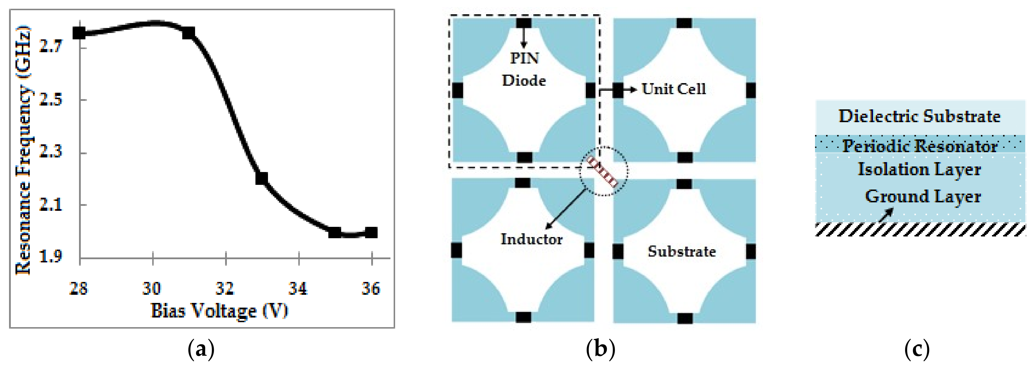
Figure 17.
(a) A unit cell of the broadband tunable AFSS absorber with of its bias lines (b) Tunable metamaterial based Active Frequency Selective Structure (AFSS) with lumped capacitors [162] (c) Reconfigurable cross dipole-hash FSS with two states by using PIN diode.
Figure 17.
(a) A unit cell of the broadband tunable AFSS absorber with of its bias lines (b) Tunable metamaterial based Active Frequency Selective Structure (AFSS) with lumped capacitors [162] (c) Reconfigurable cross dipole-hash FSS with two states by using PIN diode.

Figure 18.
(a) Top-view of AFSS with unit cell display. (b) Reconfigurable all-dielectric FSS with two states (1 and 2) and unit cell.
Figure 18.
(a) Top-view of AFSS with unit cell display. (b) Reconfigurable all-dielectric FSS with two states (1 and 2) and unit cell.

Figure 19.
(a) Fabricated two-dimensional (2D) array AFSS structure. (b) Effect on resonance frequency under different reverse bias voltages measured by parallel plate waveguide.
Figure 19.
(a) Fabricated two-dimensional (2D) array AFSS structure. (b) Effect on resonance frequency under different reverse bias voltages measured by parallel plate waveguide.

Figure 20.
3D FSS structure with one cell of graphene micro-ribbons and cross-section of the whole structure (in xy plane).
Figure 20.
3D FSS structure with one cell of graphene micro-ribbons and cross-section of the whole structure (in xy plane).

Figure 21.
(a) Photograph of the un-stretched and stretched meta-skin, wrapped around dielectric nylon rod, flexibility demonstration with a glass flask [182]. (b) Topology of the third-order stopband optical FSS. (a) Adapted from [182] and reproduced from under Creative Commons Attribution 4.0 International License.

Figure 22.
(a) Two knitted, conducting textile FSSs with conducting grid (Left), conducting patch (Right), white area knitted from polyester yarn & dark areas knitted from conducting yarn [192] (b) Microscopic image of screen printed fabric FSS [191]. (a,b) Adapted from [191,192] and reproduced by permission of the Institution of Engineering & Technology.


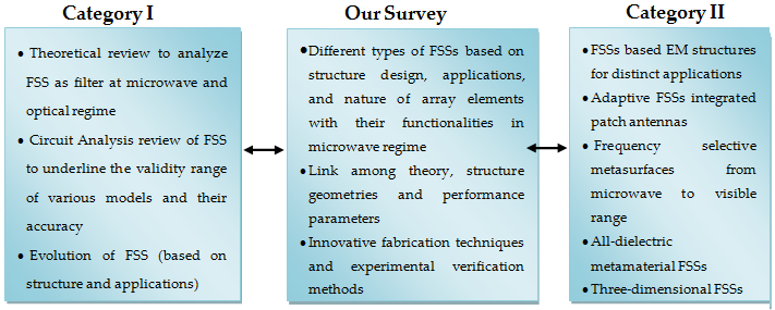
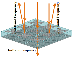
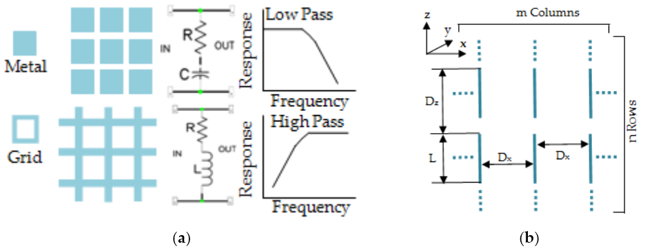
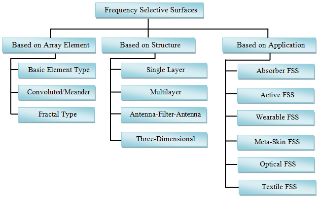
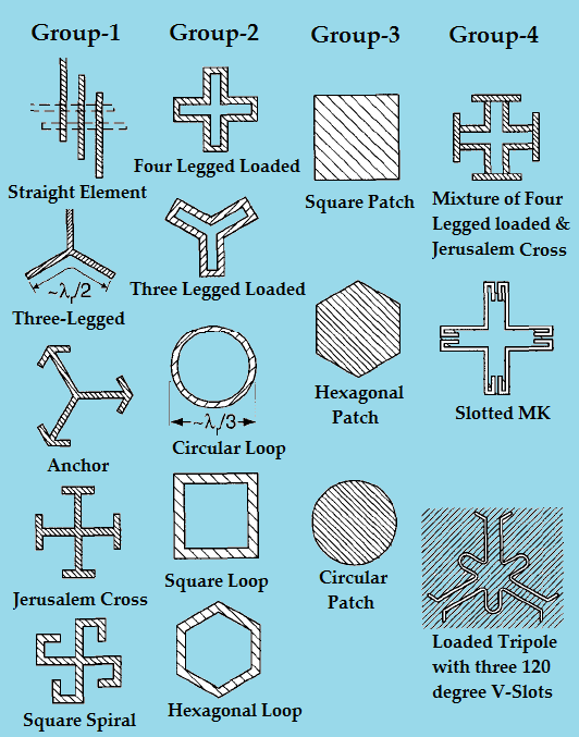
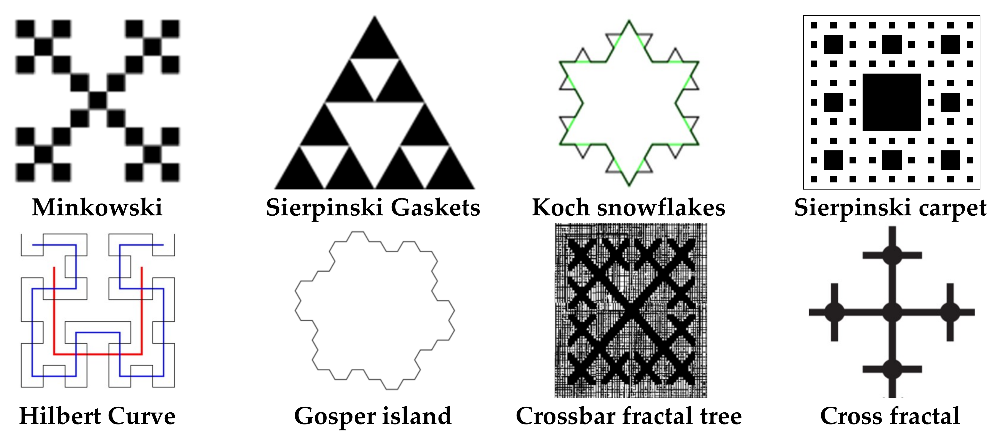
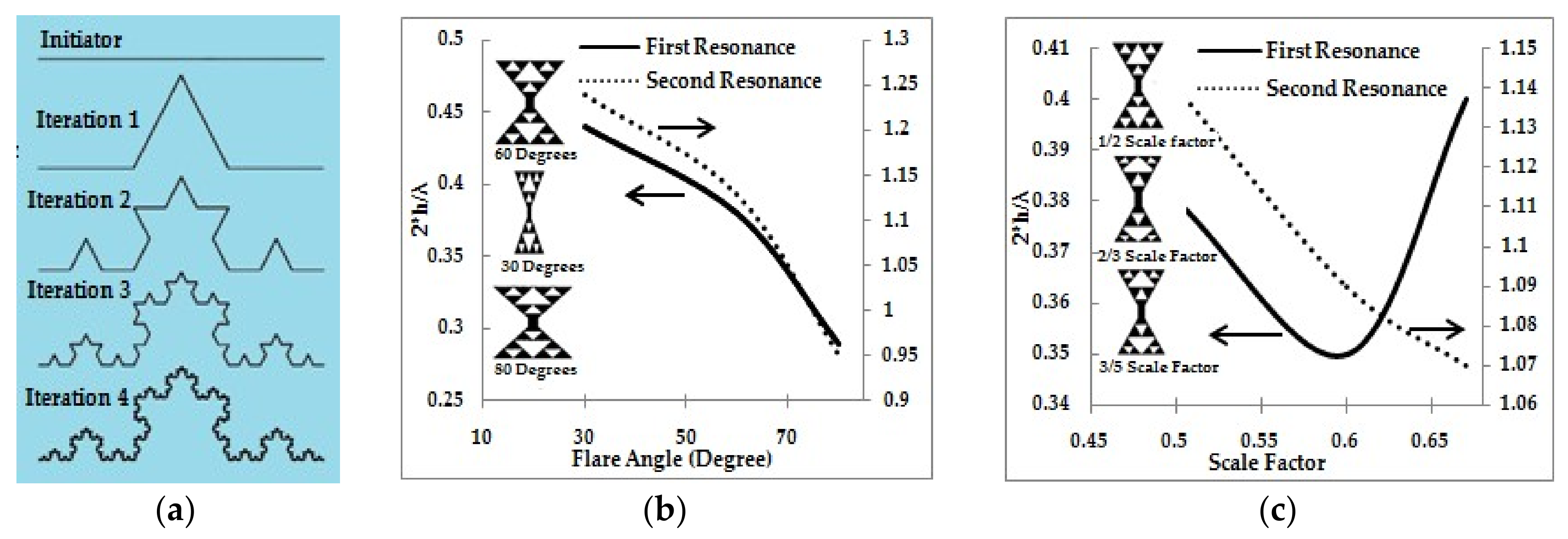
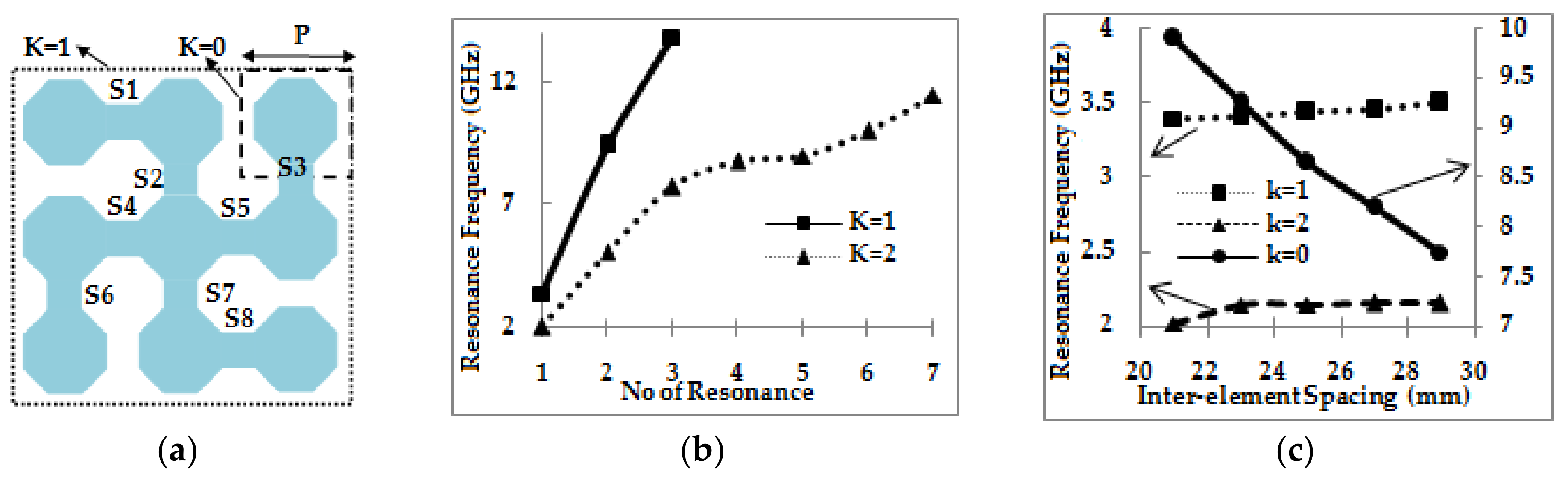
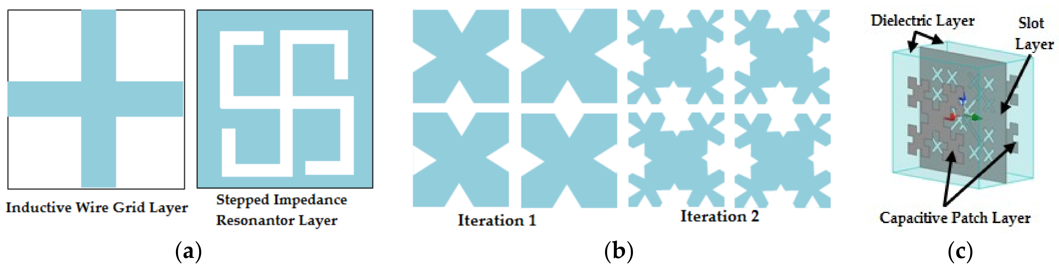
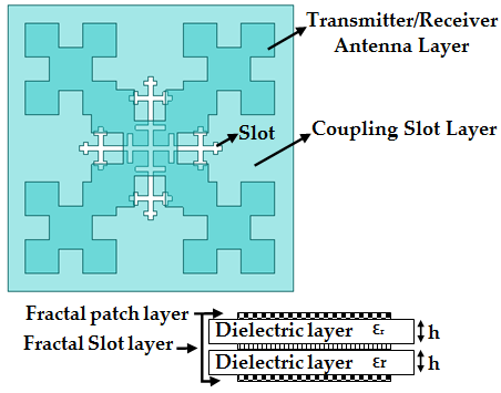
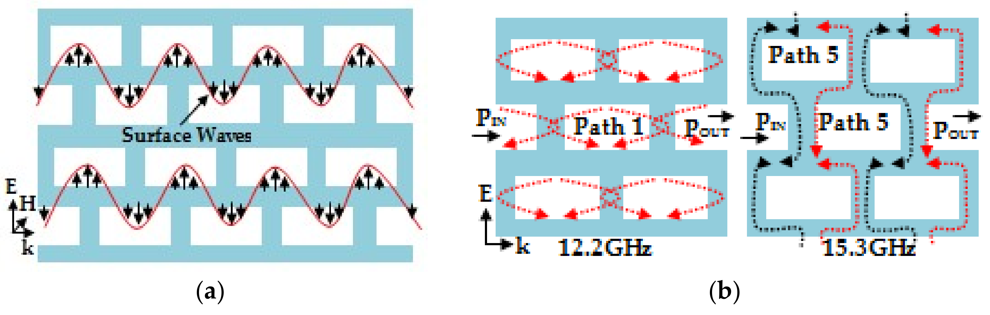
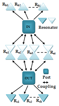
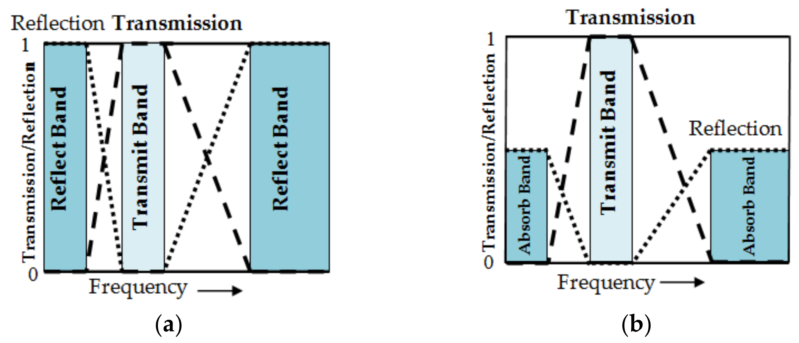
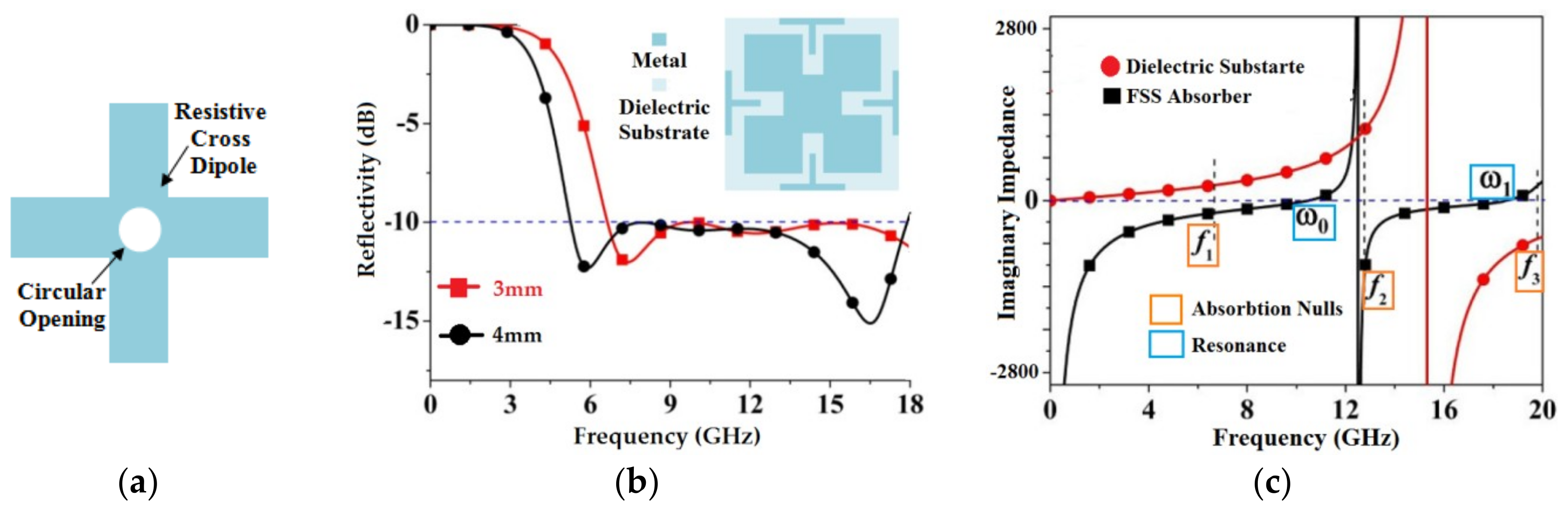
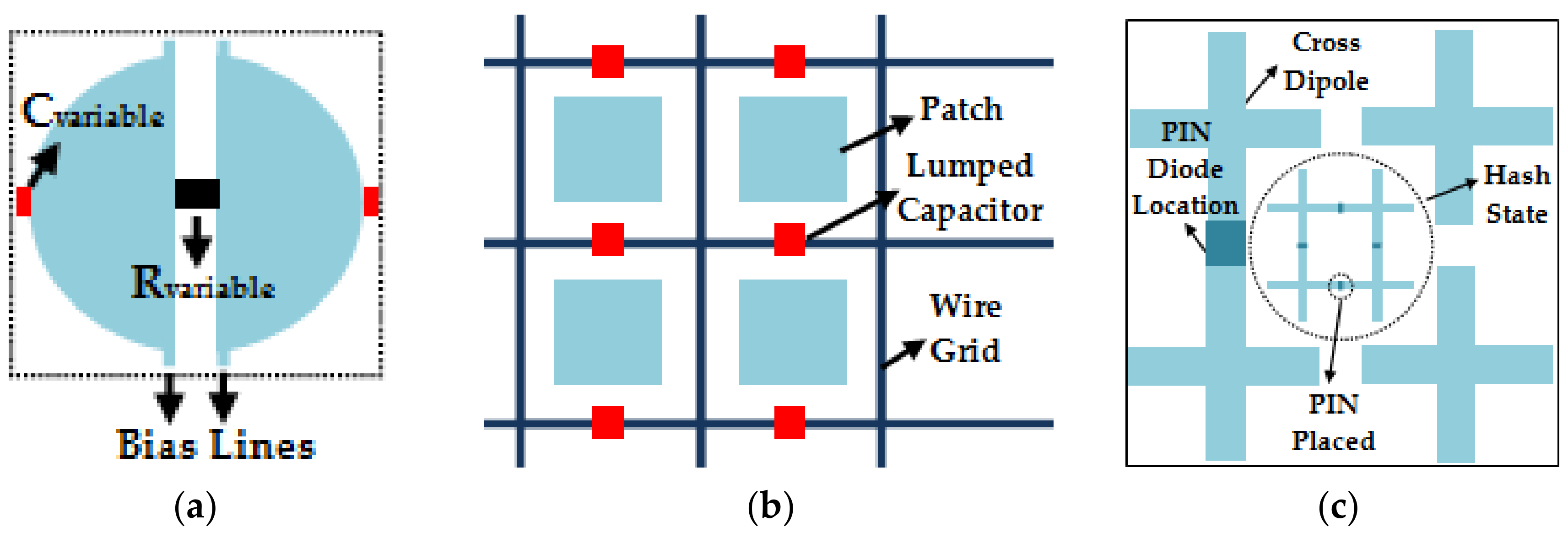
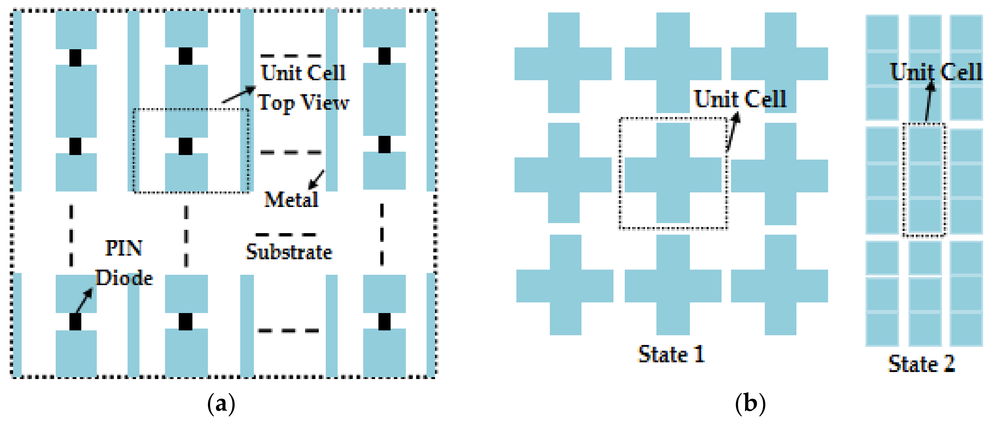
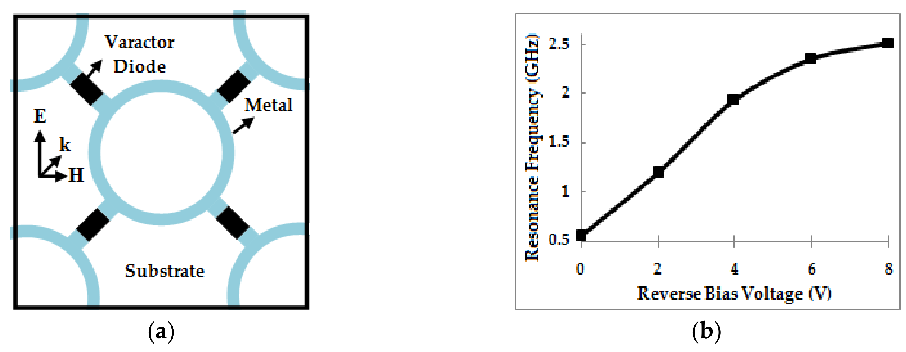
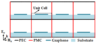
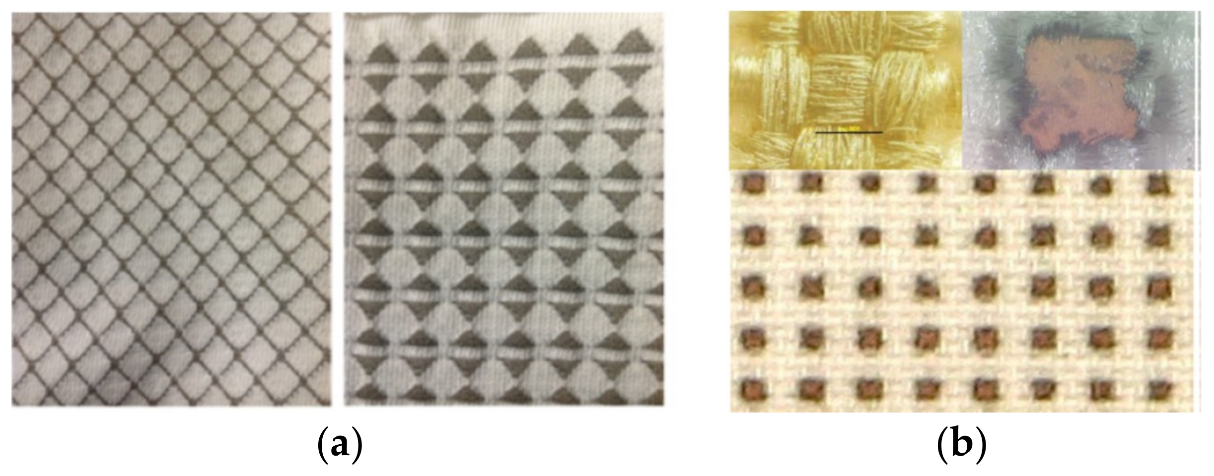
Table 1.
Summary of focused topics of frequency selective surfaces (FSSs) covered by existing surveys.
Table 1.
Summary of focused topics of frequency selective surfaces (FSSs) covered by existing surveys.
| Focused Topics | Description |
|---|---|
| Theoretical Analysis |
|
| Evolution of FSS |
|
| FSS based EM structures |
|
| Individual type of FSSs |
|
Table 2.
Different types of FSSs.
| FSS Ref. | Layers | Patch/Aperture | Filter Type |
|---|---|---|---|
| [51] | 2 | Interconnected non-complementary planes | Dual Band |
| [52] | 2 | Offset-circular ring patches | Single band |
| [53] | 1 | Centered square patch and connected L-shaped arms | Dual Band |
| [54] | 1 | Three capacitive and several inductive loops | Multi Band |
| [55] | 1 | Hexagonal-form with circular arrangement of triangular loops | Single band |
| [56] | 1 | Four sides loading aperture element into the inner side of the square loop. | Single band |
| [57] | 2 | Interconnected ring resonator element with two splits arranged orthogonally in two layers | Single band |
| [58] | 1 | Circular ring elements consisting of meander-slots with multi turns | Dual Band |
| [59] | 1 | Neighboring Y-hole elements rotated by 90° | Single band |
| [60] | 1 | Unit cell of single ring slot pair with similar three pairs concentrically used | Single band |
| [61] | 1 | Two circular loops of the nested structure with Recesses | Dual Band |
Table 3.
Different types of fractal and meandered FSSs.
| FSS Ref. | Layers | fr (GHz) | Array Element Size | Total Thickness | FBW % | Iteration | Patch and Aperture Element |
|---|---|---|---|---|---|---|---|
| [29] | 1 | 15 | 0.377λ | 0.075λ | 37 | 1 | Minkowski fractal patch |
| [64] | 1 | 4 | 0.058λ | 0.013λ | 101 | -- | Meandered spiral lines nested with neighborhood |
| [85] | 1 | 0.96 | 0.11λ | 0.005λ | 14 | 1 | Double square loop (first iteration) with folded strips at the four corners |
| [86] | 1 | 2.73 | 0.293λ | --- | 23.8 | 1 | Circular and cross dipole conductive fractal patches |
| [87] | 1 | 11.95 (stop Band) | 0.2λ | 0.002λ | 4.2 | 1 | Concentric double Minkowski fractal |
| [88] | 1 | 2.02 | 0.012λ | 0.162λ | 31 | SFD = 1.8617 | Teragon fractals |
Table 4.
Different multilayer FSSs.
| FSS Ref. | Conductive Layers | fr (GHz) | Array Element Size | Total Thickness | FBW % | Order | Patch and Aperture Elements |
|---|---|---|---|---|---|---|---|
| [93] | 3 | 10 | 0.15λ | 0.033λ | 20 | 2 | Inter-digital capacitance patch with wire grid |
| [94] | 5 | 16.5 | 0.104λ | 0.22λ | 10 | 2 | Capacitive patch and inductive wire grid |
| [96] | 3 | 3.8 | 0.076λ | 0.038λ | 10 | 2 | Patches of outer square ring with four inner stepped-impedance transmission lines and wire grid |
| [12] | 2 | 2.4 | 0.104 | 0.013 | 29.2 | -- | Meandered lines (printed patterned wires) and 4 symmetric square metal patches |
| [99] | 3 | 10.4 | 0.225λ | 0.035λ | 23 | 3 | Capacitive patches & hybrid resonator (wire grid & balanced spiral resonators) |
| [17] | 3 | 10.8 | 0.144λ × 0.125λ | 0.075λ | 75 | 2 | Connected Capacitive patches and slots of modified triples |
| [100] | 2 | 1.42 | 0.0378λ | 0.0013λ | 37 | -- | Four-fold symmetric meander lines and convoluted dipole |
| [95] | 4 | 21 | 0.21λ | 0.273λ | 5 | 2 | All wire grid layers |
| [101] | 3 | 10 | 0.1λ | 0.067λ | 21 | 2 | Double concentric square loops patch with wire grid |
| [102] | 3 | 8.5 | 0.2λ | 0.257λ | 15 | 3 | Wire grid and Hybrid (I-shaped) resonator |
| [103] | 2 | 15 | 0.3λ | 0.545λ | 13 | 2 | Gridded square loop and cross-loop aperture embedded in five dielectric substrate layers |
| [104] | 2 | 7.95 | 0.12λ | 0.042λ | 23 | -- | Crossed slot element convoluted three circles with vertical vias |
| [105] | 2 | 12.24 | 0.245λ | 0.03λ | 96 | -- | Patch of four square loops at four corners and non-resonant inductive layer with a square loop |
| [97] | 2 | 45.91 | 0.53λ | 0.055λ | 28.4 | -- | Fractal Koch elements cascaded with air gap in between |
Table 5.
Comparison of Antenna-Filter-Antenna fractal FSS structures.
| FSS Ref. | Conducting Layers | f0 (GHz) | Array Element Size | Total Thickness | FBW % | Order | Patch and Aperture Elements |
|---|---|---|---|---|---|---|---|
| [75] | 5 | 10 | 0.25λ | 0.267λ | 37 | 3 | Minkowski fractal patch with slot ground |
| [74] | 3 | 5.1 | 0.2λ | 0.07λ | 19.6 | 2 | Minkowski fractal patch with slot ground |
| [107] | 3 | 36 | 0.632λ | 0.116λ | 8.2 (1 dB) | -- | Hexagonal patch and CPW quarter wave resonator (U slot) |
| [98] | 3 | 10 | 0.25λ | 0.23λ | 60 | 3 | Fractal patch with slotted ground |
Table 6.
An overview of 3D FSSs reported in different researches.
| FSS Ref. | 3D FSS | Element Type | 3 dB BW Range (GHz) |
|---|---|---|---|
| [112] | Wide passband FSS | Two microstrip lines split by a horizontally laid long and thin metallic rectangular bar | 5–10 |
| [111] | Passband FSS with rapid roll-off based on surface wave tunneling | Subwavelength staggered vertical and horizontal metallic rectangular frames | 11.8–13.2 |
| [127] | Miniaturized, thinner FSS with steep quasi-elliptical band-stop filtering | Lumped capacitor on microstrip stepped-impedance resonator | 4.3–4.8 |
| [128] | Flat passband and sharp rejection response FSS | A symmetric unit cell in three dimensions | 12.4–16.3 |
| [129] | Wide and flat passband FSS | Periodic array of square waveguides | 12–24.7 |
| [22] | Wide passband with four transmission poles | Two parallel U-shaped suspended strip lines, double printed on a thin substrate and located inside a square waveguide | 8.4–16.2 |
| [130] | Novel miniaturized 3D FSS independent of polarizations & incident angles | Square metallic waveguide with modified dumbbell slots in all waveguide walls | 3.7–4 |
| [131] | Dual-polarized FSS with wide out-of-band rejection | Two arrays of vertically and horizontally placed double sided parallel strip lines connected together by a centered via and a number of inserted metallic plates | 7–8.3 |
Table 7.
An overview of microwave FSS absorbers.
| FSS Ref. | Type of Microwave Absorber | Element Type |
|---|---|---|
| [140] | Wide Incidence angle insensitive dual polarized two layers MM absorber | Symmetric geometry of eight-circular sectors and Bottom ground plane |
| [141] | Miniaturized FSS absorber | Minkowski fractal loops |
| [142] | Resistive FSS with Ferromagnetic nan-ofilms based on high-impedance surfaces | A square patch of capacitive impedance. |
| [143] | Lightweight, ultra-broadband, wide incidence angle resistive FSS absorber based on topology optimization | Resistive patches on top, middle Polyurethane foam substrate & metal ground on bottom |
| [144] | Ultra-thin absorber with cascaded high impedance & FSS | Pixelized metallic surface placed above the high impedance surface |
| [145] | Polarization dependent FSS absorber with multiple absorption peaks | C shaped slot in a circular patch, ground bottom and polyimide film as dielectric substrate |
| [146] | FSS absorber with low profile | Capacitive patches and inductive mesh |
| [147] | Compact broadband FSS absorber | Resistively loaded quadruple hexagonal loops |
| [148] | Ultra compact partly transmissible absorptive FSS at 5-GHz Wi-Fi band, to solve EMI/RFI problems in mixed-signal systems. | Via-based structure with staggered patterns on front and back metal layer while back metal layer has air vents in the ground plane |
| [149] | Thin broadband FSS embedded absorber | Double layer composite coating of higher iteration of Sierpinski gasket patches |
| [150] | High absorptive FSS embedded absorber | Fractal FSS with top metal and bottom Aluminum metal plate |
Table 8.
An overview of AFSS with their applications.
| FSS Ref. | AFSS | Element Type and Configuration | Frequency (Range) | Applications |
|---|---|---|---|---|
| [169] | Reconfigurable FSS with two states (stopband) | Cross-dipole element (Reconfigurable cross dipole & hash simply by changing the state of PIN diode) (1 layer) | 12.61 (12–13) GHz | Adaptive & RFID antennas |
| [23] | Single-layer single polarized AFSS (Pass band) | Circular aperture with four PIN diodes placed orthogonally (1 layer) | 2.63 (2–3) GHz | Intelligent spectrum selective island |
| [168] | Reconfigurable by orthogonal rotation, all-dielectric MM AFSS (stopband) | Cross-shaped high-permittivity ceramic resonators (No metal layer) | (3.55–4.60) & (4.54–4.94) GHz | RCS reduction, reconfigurable antenna systems, high temperature & high power environment. |
| [139] | Tunable broadband polarization insensitive absorber | Four quarter circles and plates create the gaps, series PIN diodes as variable resistor and inductors place between two metallic plates for isolation (2 layers) | (1.6–8) GHz | Stealth technology & EM shielding |
| [162] | Tunable MM based AFSS (Passband) | An array of metallic square loops, a wire grid and lumped, variable capacitors inserted in the gap between the loops (2 layers) | 8.49–11.48 GHz | X band |
| [159] | 3D tunable FSS (Stopband) | 2D array of vertical graphene micro-ribbons, tunable by change of chemical potential | 21.787–24.088 THz (BW = 1.2) | Terahertz band |
| [164] | Tunable AFSS absorber | Pattern with gradational edges and PIN diode as variable resistor, Varactor diode as a variable capacitor (2 layers) | (1–5) GHz | Smart stealth systems |
| [170] | Frequency tunable Metamaterial Absorber with high absorption ratio. | Metallic patterns, a liquid metalalloy Eutectic Gallium-Indium (EGaIn) injected in a micro-fluidic channel, engraved on Polymethyl Methacrylate | 10.96–10.61 GHz | Large area sensor applications with micro-pumps |
Table 9.
An overview of types of AFSS with the comparison of their FBW and tuning range (TRs).
| FSS Ref. | Type of AFSS | Switching/Tuning Element Used | FBW% | Tuning Range % | Polarization Insensitivity |
|---|---|---|---|---|---|
| [169] | Switchable | PIN diode | 2 (−20 dB), (fr = 12.6 GHz) | -- | Yes |
| [151] | Switchable | PIN diode | 40 (−5 dB) | -- | No |
| [156] | Switchable Absorber/Reflector | PIN diode | 79.5 (−10 dB) | -- | Yes |
| [154] | Switchable | PIN diode | 39.1 (−3 dB) | -- | No |
| [155] | Switchable | PIN diode | 7.3 (−15 dB) | -- | Yes |
| [157] | Switchable Absorber | PIN diode | 65 (−10 dB) | -- | No |
| [23] | Switchable (Passband) | PIN diodes | 17 (−5 dB), (fr = 2.63 GHz) | -- | N0 |
| [171] | Tunable (Stopband) | Varactor diode | 12.5 (−10 dB) | 32 | No |
| [177] | Tunable Absorber (Passband) | Varactor diode | 4 (−5 dB) | 5 | No |
| [176] | Tunable (Stopband) | Varactor diode | 81.4 (−10 dB) | 69.5 | No |
| [172] | Tunable | Varactor diode | 152.4 (−20 dB) | 129 | Yes |
| [168] | Tunable (Stopband) | High-permittivity ceramics | 25.8 (First state), 8.4 (Second State (−10 dB) | 22.9 (1st Resonance) | No |
| [139] | Tunable Absorber | PIN diode | 91 (−10 dB) | 31.6 | Yes |
| [162] | Tunable (Passband) | Chip capacitor | 5.9 (−5 dB), (fr = 8.5 GHz) | 30 | No |
| [159] | 3D Tunable AFSS (Stopband) | Graphene micro-ribbons | 5.5 (0.5 S21max) | 10 | No |
| [164] | Tunable Absorber | PIN, Varactor diode | 113 (−10 dB) | 47.3 | No |
| [175] | Tunable 3D AFSS (Passband) | Varactor diode | 14 (−3 dB) (fr = 2.75 GHz) | 65 | No |
| [163] | Tunable (Passband) | Varactor diode | 11.5 (0.5 S21max) | 24.6 | No |
Table 10.
Summary of the key factors linking the structure geometries, and performance characteristics.
Table 10.
Summary of the key factors linking the structure geometries, and performance characteristics.
| Category | Factor | Impact/Outcomes |
|---|---|---|
| Type of array element | Slot element | Passband |
| Patch element | Stopband | |
| Large Loop element | High BW | |
| Hexagonal Loop | Wide band | |
| Loaded 3 or 4 Legged element | Narrow band | |
| Meandered/Convoluted element | Unit cell size reduction but manufacturing limitation may occur | |
| Fractals patch | Reduces the electrical length, Inter-element spacing (IES) & so resonant frequency | |
| Self similar feature of fractal | Multiband response but drawback of early appearance of grating lobes | |
| Dissimilar fractal geometric patterns in single FSS | Double/Multiband response | |
| Tunable FSS (Active element based) | Tunability in polarization and resonant frequency | |
| Active element in AFSS | Deviation in operating frequency, power management issues, high insertion losses and erroneous response | |
| Array profile | Reduce the IES of gangbuster | Large BW and delay in onset of grating lobes |
| Reduce the Unit cell (small electrical dimensions) | High angular stability | |
| Increase in periodicity | BW and resonant frequency reduces, higher distortion and early onset of grating lobes | |
| Electrically subwavelength array separation at resonant frequency | Elimination of unwanted interference Nulls | |
| Decrease of IES | Stable resonant frequency, delayed onset of grating lobes | |
| IES variation | BW change | |
| Circumference of element change | Effect on electrical length & so resonant frequency | |
| Structure profile | Cascaded surfaces | Faster roll-off |
| Multilayer FSS (stacking structure) | Increase in BW | |
| AFA configuration | Higher selectivity and BW | |
| 3D FSS | Complex structures but faster roll-off, stable response (In- and out-band) | |
| Air gap separation | BW variation | |
| Dielectric profile | No dielectric substrate | Unstable BW of transmission curves |
| Dielectric Profile & IES | Defines the ripples (Flatness of response) | |
| Low dielectric constant | Constant BW with AOI | |
| High dielectric constant | More angular stability |
Table 11.
Practical applications of FSSs.
| FSS Ref. | Application | FSS Ref. | Application |
|---|---|---|---|
| [162,168,194] | MMs FSS | [117,119,154,195] | FSS for mobile communication |
| [10,196,197] | MM/MSs Lens | [50,162,177] | X band |
| [191,192,193] | Textile FSS | [74,198] | C band |
| [188,189,190] | Optical FSS/MSs | [11] | 5G EMI reduction |
| [186] | Near Infrared | [168] | RCS reduction |
| [184,185] | Infrared | [61,88,155] | Secure wireless network |
| [187] | Multi spectral filter/Mirrors/Anti-reflecting coating | [25,123,199,200,201] | RF interference and harmonic suppression |
| [179,180,181,182] | Wearable FSS | [11,91,151,172] | EMI shielding |
| [139,140,145,150] | FSS absorber | [202] | Radio Astronomy |
| [28,126] | Sensors | [8] | Dichroic sub-reflector |
| [9,116,178] | RFID | [159,160] | Terahertz band |
| [77,118,124,169,174] | FSS antenna | [75,103,121,139,164] | Stealth radome |
| [154] | Electrically reconfigurable mechanisms | [122] | Wireless charging of portable devices |
© 2018 by the authors. Licensee MDPI, Basel, Switzerland. This article is an open access article distributed under the terms and conditions of the Creative Commons Attribution (CC BY) license (http://creativecommons.org/licenses/by/4.0/).
Share and Cite
MDPI and ACS Style
Anwar, R.S.; Mao, L.; Ning, H. Frequency Selective Surfaces: A Review. Appl. Sci. 2018, 8, 1689. https://doi.org/10.3390/app8091689
AMA Style
Anwar RS, Mao L, Ning H. Frequency Selective Surfaces: A Review. Applied Sciences. 2018; 8(9):1689. https://doi.org/10.3390/app8091689
Chicago/Turabian StyleAnwar, Rana Sadaf, Lingfeng Mao, and Huansheng Ning. 2018. "Frequency Selective Surfaces: A Review" Applied Sciences 8, no. 9: 1689. https://doi.org/10.3390/app8091689
Note that from the first issue of 2016, this journal uses article numbers instead of page numbers. See further details here.