Determination of Interface-State Distributions in Polymer-Based Metal-Insulator-Semiconductor Capacitors by Impedance Spectroscopy

 , ,
, , 
Abstract
:1. Introduction
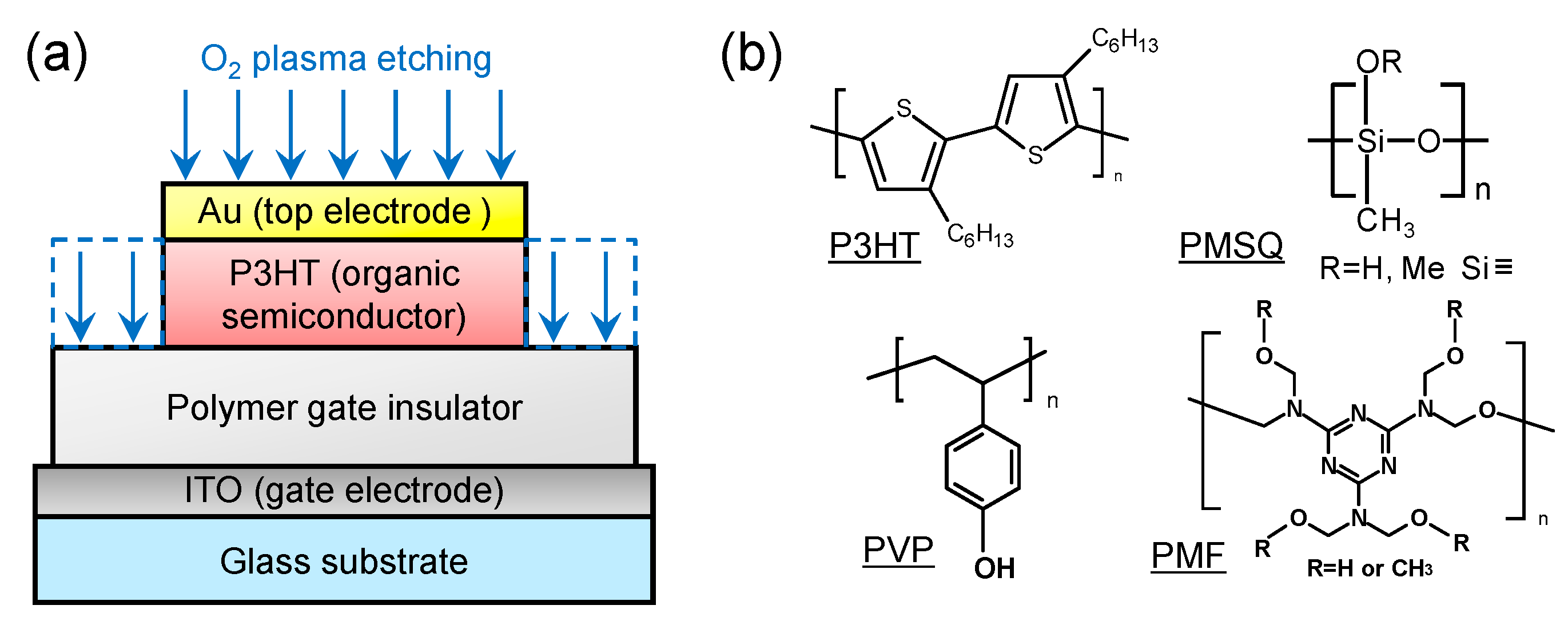
2. Experimental
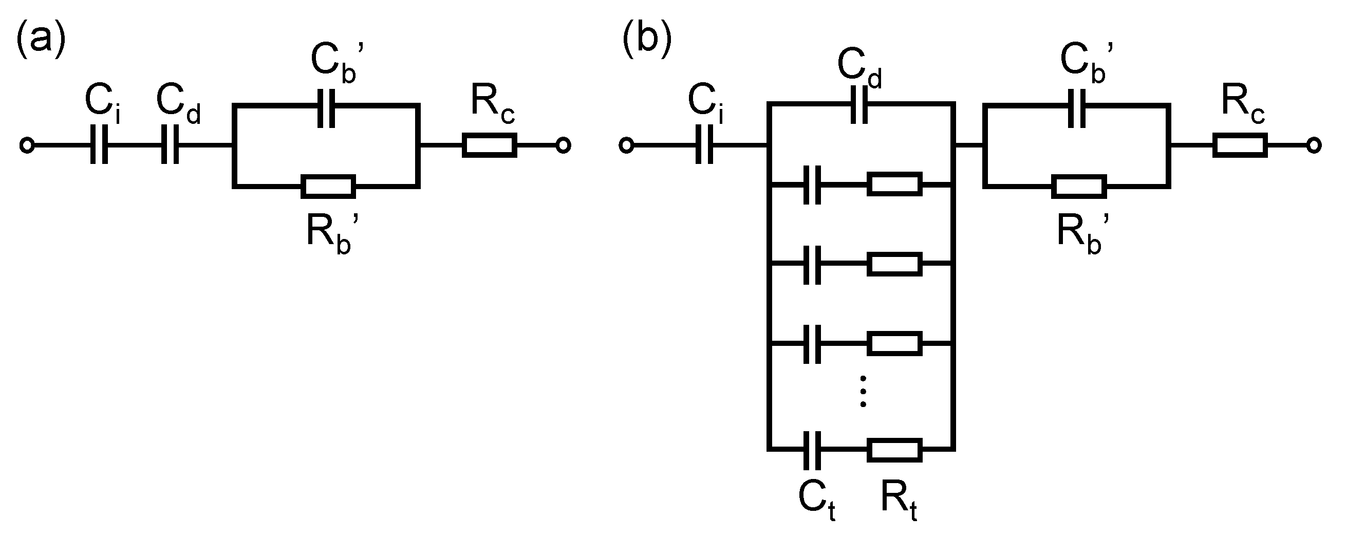
3. Results and Discussion
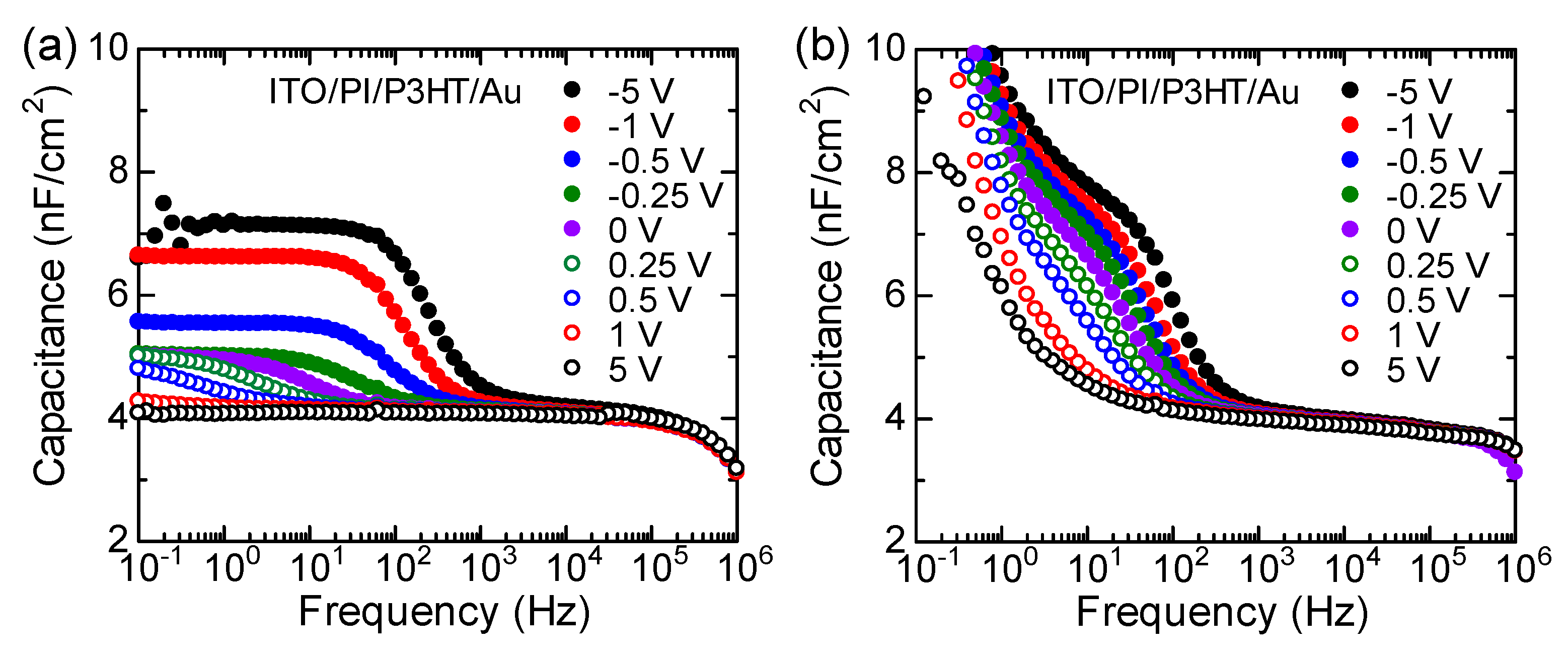
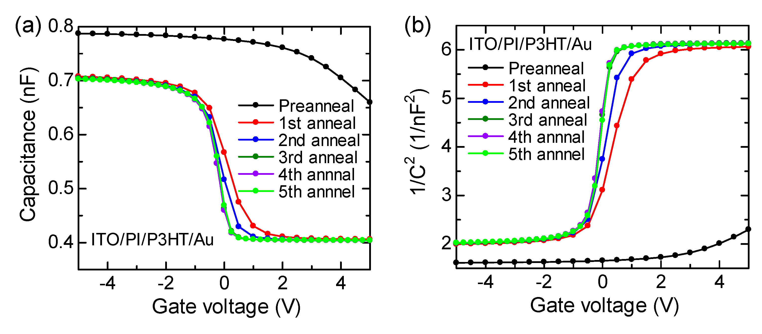
3.1. Optimization of the Fabrication Processes of Organic MIS Capacitors
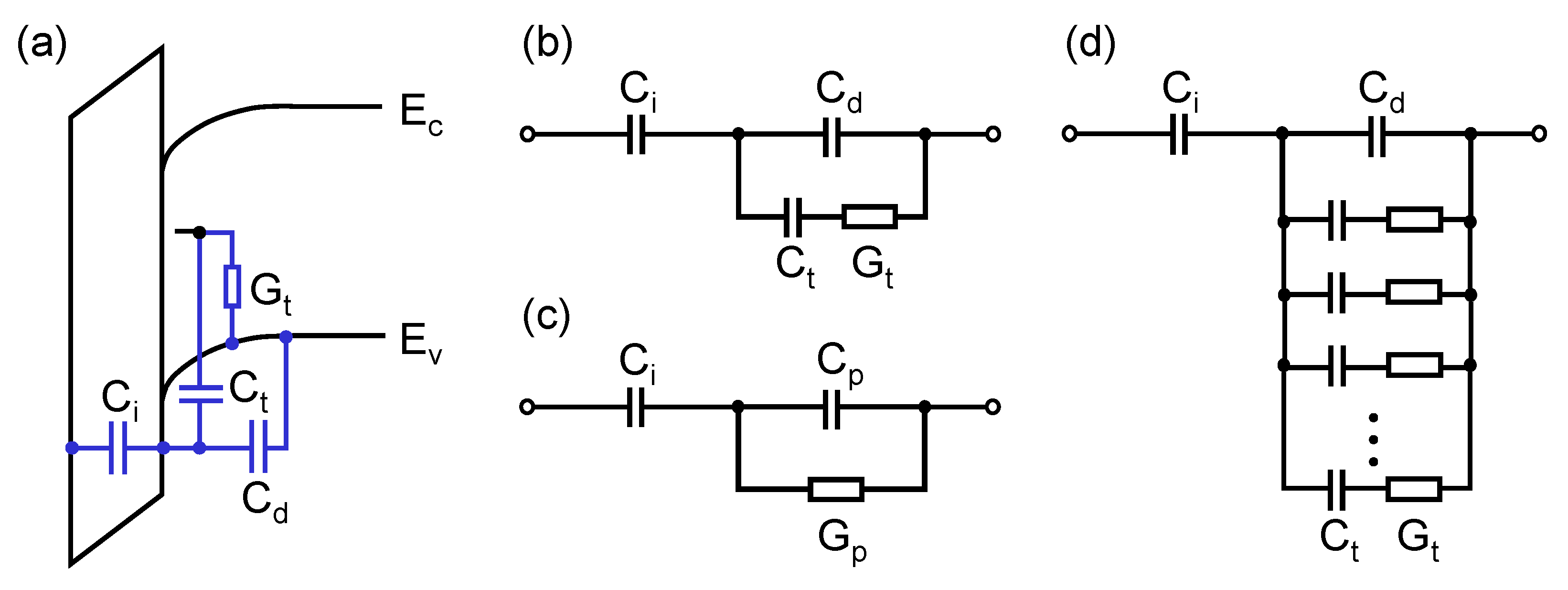
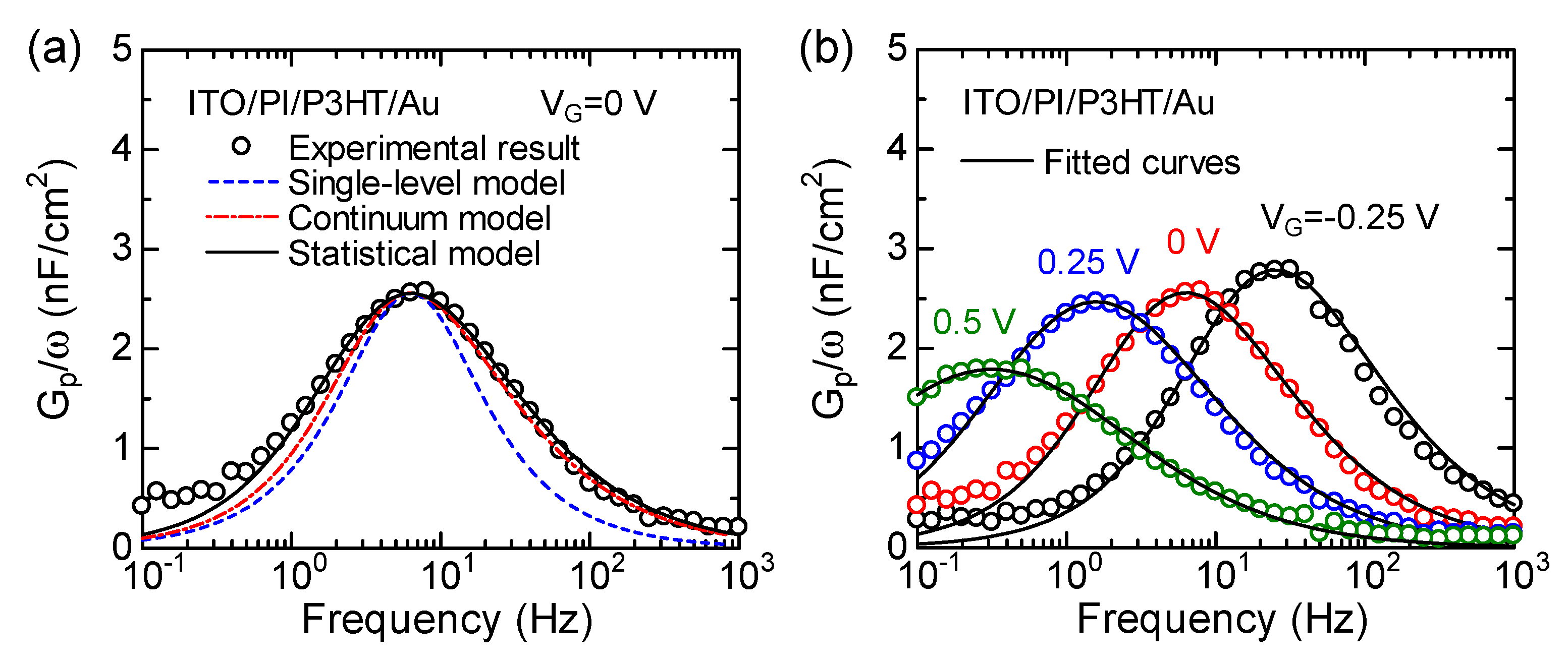
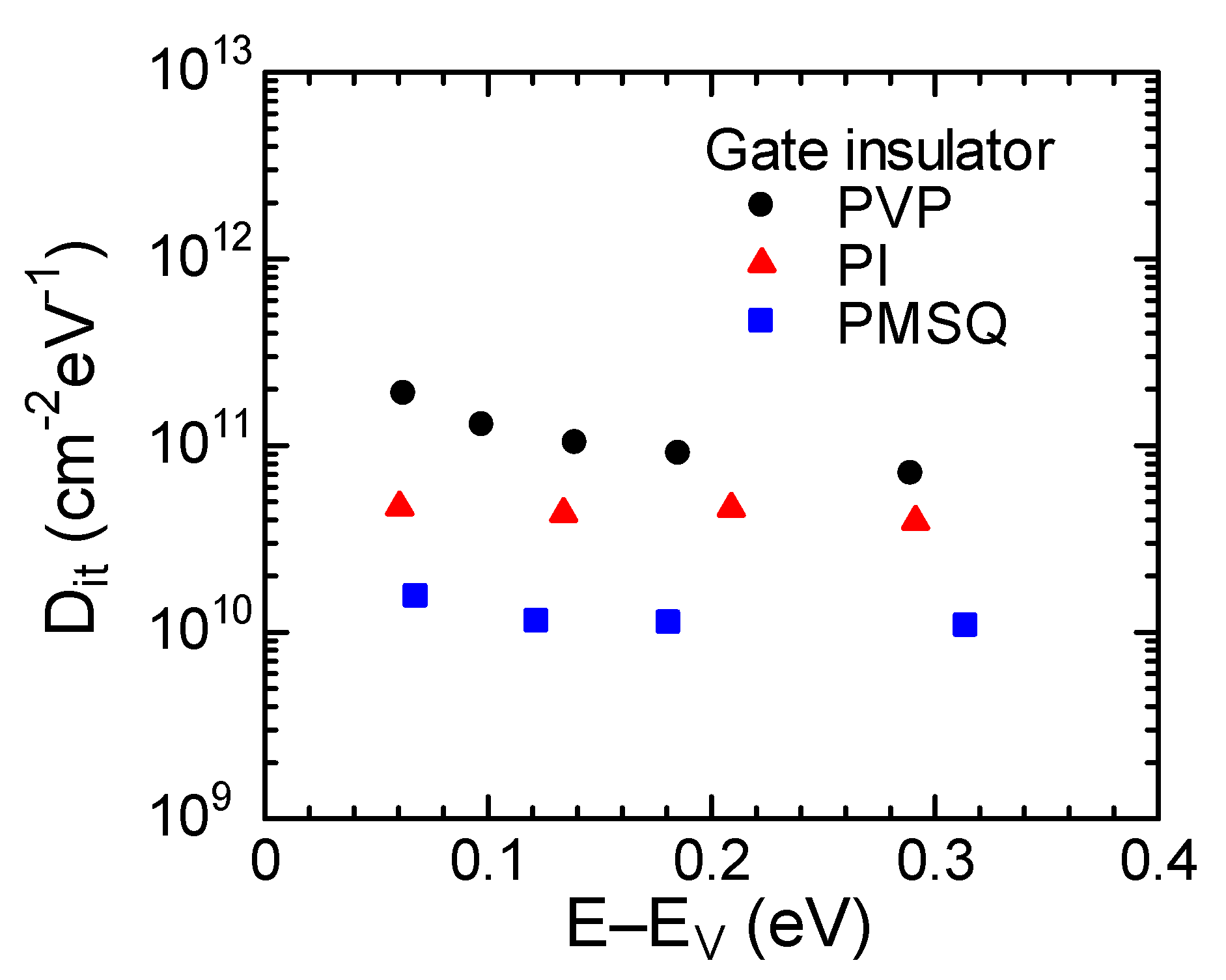
3.2. Determination of the Interface States of MIS Capacitors with Different Polymer Gate Insulators
4. Conclusions
Author Contributions
Funding
Acknowledgments
Conflicts of Interest
References
- Sirringhaus, H. Organic field-effect transistors: The path beyond amorphous silicon. Adv. Mater. 2014, 26, 1319–1335. [Google Scholar] [CrossRef] [PubMed]
- Klauk, H. Organic thin-film transistors. Chem. Soc. Rev. 2010, 39, 2643–2666. [Google Scholar] [CrossRef] [PubMed]
- Veres, J.; Ogier, S.; Lloyd, G.; de Leeuw, D. Gate insulators in organic field-effect transistors. Chem. Mater. 2004, 16, 4543–4555. [Google Scholar] [CrossRef]
- Kline, R.J.; McGehee, M.D.; Toney, M.F. Highly oriented crystals at the buried interface in polythiophene thin-film transistors. Nat. Mater. 2006, 5, 222–228. [Google Scholar] [CrossRef]
- Jung, Y.; Kline, R.J.; Fischer, D.A.; Lin, E.K.; Heeney, M.; McCulloch, I.; DeLongchamp, D.M. The effect of interfacial roughness on the thin film morphology and charge transport of high-performance polythiophenes. Adv. Funct. Mater. 2008, 18, 742–750. [Google Scholar] [CrossRef]
- Sheraw, C.D.; Gundlach, D.J.; Jackson, T.N. Spin-on polymer gate dielectric for high performance organic thin film transistors. Mater. Res. Soc. Symp. Proc. 2000, 558, 403–408. [Google Scholar] [CrossRef]
- Sekitani, T.; Iba, S.; Kato, Y.; Someya, T. Bending effect of organic field-effect transistors with polyimide gate dielectric layers. Jpn. J. Appl. Phys. 2005, 44, 2841–2843. [Google Scholar] [CrossRef]
- Klauk, H.; Halik, M.; Zschieschang, U.; Schmid, G.; Radlik, W.; Weber, W. High-mobility polymer gate dielectric pentacene thin film transistors. J. Appl. Phys. 2002, 92, 5259–5263. [Google Scholar] [CrossRef]
- Bao, Z.; Kuck, V.; Rogers, J.A.; Paczkowski, M.A. Silsesquioxane resins as high-performance solution processible dielectric materials for organic transistor applications. Adv. Funct. Mater. 2002, 12, 526–531. [Google Scholar] [CrossRef]
- Tomatsu, K.; Hamada, T.; Nagase, T.; Yamazaki, S.; Kobayashi, T.; Murakami, S.; Matsukawa, K.; Naito, H. Fabrication and characterization of poly(3-hexylthiophene)-based field-effect transistors with silsesquioxane gate insulators. Jpn. J. Appl. Phys. 2008, 47, 3196–3199. [Google Scholar] [CrossRef]
- Nagase, T.; Hamada, T.; Tomatsu, K.; Yamazaki, S.; Kobayashi, T.; Murakami, S.; Matsukawa, K.; Naito, H. Low-temperature processable organic-inorganic hybrid gate dielectrics for solution-based organic field-effect transistors. Adv. Mater. 2010, 22, 4706–4710. [Google Scholar] [CrossRef] [PubMed]
- Matsukawa, K.; Watanabe, M.; Hamada, T.; Nagase, T.; Naito, H. Polysilsesquioxanes for gate-insulating materials of organic thin-film transistors. Int. J. Polym. Sci. 2012, 2012, 852063. [Google Scholar] [CrossRef]
- Meijer, E.J.; Mangnus, A.V.G.; Hart, C.M.; de Leeuw, D.M.; Klapwijk, T.M. Frequency behavior and the Mott–Schottky analysis in poly(3-hexyl thiophene) metal–insulator–semiconductor diodes. Appl. Phys. Lett. 2001, 78, 3902–3904. [Google Scholar] [CrossRef]
- Torres, I.; Taylor, D.M.; Itoh, E. Interface states and depletion-induced threshold voltage instability in organic metal-insulator-semiconductor structures. Appl. Phys. Lett. 2004, 85, 314–316. [Google Scholar] [CrossRef]
- Torres, I.; Taylor, D.M. Interface states in polymer metal-insulator-semiconductor devices. J. Appl. Phys. 2005, 98, 073710. [Google Scholar] [CrossRef]
- Itoh, E.; Torres, I.; Taylor, D.M. The influence of interfacial charge exchange phenomena at the insulator-semiconductor interface on the electrical properties of poly(3-hexylthiophene) based field effect transistors. Jpn. J. Appl. Phys. 2005, 44, 641–647. [Google Scholar] [CrossRef]
- Yun, M.; Gangopadhyay, S.; Bai, M.; Taub, H.; Arif, M.; Guha, S. Interface states in polyfluorene-based metal-insulator-semiconductor devices. Org. Electron. 2007, 8, 591–600. [Google Scholar] [CrossRef]
- Alves, N.; Taylor, D.M. Determining the interfacial density of states in metal-insulator-semiconductor devices based on poly(3-hexylthiophene). Appl. Phys. Lett. 2008, 92, 103312. [Google Scholar] [CrossRef] [Green Version]
- Nicollian, E.H.; Goetzberger, A. The Si-SiO2 interface—Electrical properties as determined by the metal-insulator-silicon conductance technique. Bell. Syst. Tech. J. 1967, 46, 1055–1133. [Google Scholar] [CrossRef]
- Nicollian, E.H.; Brews, J.R. MOS (Metal Oxide Semiconductor) Physics and Technology; Wiley Interscience: New York, NY, USA, 2003; ISBN 978-0-471-43079-7. [Google Scholar]
- Noh, Y.-Y.; Kim, D.-Y.; Yase, K. Highly sensitive thin-film organic phototransistors: Effect of wavelength of light source on device performance. J. Appl. Phys. 2005, 98, 074505. [Google Scholar] [CrossRef]
- Nicollian, E.H.; Goetzberger, A. Lateral AC current flow model for metal-insulator-semiconductor capacitors. IEEE Trans. Electron. Devices 1965, 12, 108–117. [Google Scholar] [CrossRef]
- Itoh, E.; Torres, I.; Hayden, C.; Taylor, D.M. Excimer-laser micropatterned photobleaching as a means of isolating polymer electronic devices. Synth. Met. 2006, 156, 129–134. [Google Scholar] [CrossRef]
- Jung, K.-D.; Lee, C.A.; Park, D.-W.; Park, B.-G.; Shin, H.; Lee, J.D. Admittance measurements on OFET channel and its modeling with R–C network. IEEE Electron Device Lett. 2007, 28, 204–206. [Google Scholar] [CrossRef]
- Hoshino, S.; Yoshida, M.; Uemura, S.; Kodzasa, T.; Takada, N.; Kamata, T.; Yase, K. Influence of moisture on device characteristics of polythiophene-based field-effect transistors. J. Appl. Phys. 2004, 95, 5088–5093. [Google Scholar] [CrossRef]
- Sze, S.M.; Ng, K.K. Physics of Semiconductor Devices, 3rd ed.; John Wiley & Sons, Inc.: New York, NY, USA, 2007; ISBN 978-0-471-14323-9. [Google Scholar]
- Grecu, S.; Roggenbuck, M.; Opitz, A.; Brütting, W. Differences of interface and bulk transport properties in polymer field-effect devices. Org. Electron. 2006, 7, 276–286. [Google Scholar] [CrossRef] [Green Version]
- Nicollian, E.H.; Goetzberger, A.; Lopez, A.D. Expedient method of obtaining interface state properties from MIS conductance measurements. Solid-State Electron. 1969, 12, 937–944. [Google Scholar] [CrossRef]
- Simonne, J.J. A method to extract interface state parameters from the MIS parallel conductance technique. Solid-State Electron. 1973, 16, 121–124. [Google Scholar] [CrossRef]
- Berglund, C.N. Surface states at steam-grown silicon-silicon dioxide interfaces. IEEE Trans. Electron Devices 1966, 13, 701–705. [Google Scholar] [CrossRef]
- Shur, M.; Hack, M. Physics of amorphous silicon based alloy field-effect transistors. J. Appl. Phys. 1984, 55, 3831–3842. [Google Scholar] [CrossRef]


| Annealing Cycle | NA (cm−3) |
|---|---|
| Before annealing | 1.6 × 10¹⁶ |
| 1st | 2.8 × 10¹⁵ |
| 2nd | 2.0 × 10¹⁵ |
| 3rd | 1.4 × 10¹⁵ |
| 4th | 1.4 × 10¹⁵ |
| 5th | 1.4 × 10¹⁵ |
| Insulator | µ (cm2 V‒1 s‒1) | SS (V/decade) | WCA (degree) |
|---|---|---|---|
| PMSQ | 1.0 × 10⁻² | 4.7 | 93 |
| PI | 1.7 × 10⁻³ | 7.3 | 80 |
| PVP | 1.0 × 10⁻⁴ | 9.3 | 64 |
© 2018 by the authors. Licensee MDPI, Basel, Switzerland. This article is an open access article distributed under the terms and conditions of the Creative Commons Attribution (CC BY) license (http://creativecommons.org/licenses/by/4.0/).
Share and Cite
Hatta, H.; Miyagawa, Y.; Nagase, T.; Kobayashi, T.; Hamada, T.; Murakami, S.; Matsukawa, K.; Naito, H. Determination of Interface-State Distributions in Polymer-Based Metal-Insulator-Semiconductor Capacitors by Impedance Spectroscopy. Appl. Sci. 2018, 8, 1493. https://doi.org/10.3390/app8091493
Hatta H, Miyagawa Y, Nagase T, Kobayashi T, Hamada T, Murakami S, Matsukawa K, Naito H. Determination of Interface-State Distributions in Polymer-Based Metal-Insulator-Semiconductor Capacitors by Impedance Spectroscopy. Applied Sciences. 2018; 8(9):1493. https://doi.org/10.3390/app8091493
Chicago/Turabian StyleHatta, Hideyuki, Yuhi Miyagawa, Takashi Nagase, Takashi Kobayashi, Takashi Hamada, Shuichi Murakami, Kimihiro Matsukawa, and Hiroyoshi Naito. 2018. "Determination of Interface-State Distributions in Polymer-Based Metal-Insulator-Semiconductor Capacitors by Impedance Spectroscopy" Applied Sciences 8, no. 9: 1493. https://doi.org/10.3390/app8091493