Optimized Multiport DC/DC Converter for Vehicle Drivetrains: Topology and Design Optimization
by
 , , and
Duong Tran
1,2, 
Sajib Chakraborty
1,2 ,
,
Yuanfeng Lan
1,2 ,
,
Joeri Van Mierlo
1,2 and
and
Omar Hegazy
1,2,* 1
Department of Electrical Machines and Energy Technology (ETEC) & MOBI Research Group, Vrije Universiteit Brussel (VUB), Pleinlaan 2, Brussels 1050, Belgium
2
Flanders Make, Heverlee 3001, Belgium
*
Author to whom correspondence should be addressed.
Appl. Sci. 2018, 8(8), 1351; https://doi.org/10.3390/app8081351
Submission received: 20 June 2018
/
Revised: 7 August 2018
/
Accepted: 9 August 2018
/
Published: 11 August 2018
(This article belongs to the Special Issue Plug-in Hybrid Electric Vehicle (PHEV))
Abstract
:DC/DC Multiport Converters (MPC) are gaining interest in the hybrid electric drivetrains (i.e., vehicles or machines), where multiple sources are combined to enhance their capabilities and performances in terms of efficiency, integrated design and reliability. This hybridization will lead to more complexity and high development/design time. Therefore, a proper design approach is needed to optimize the design of the MPC as well as its performance and to reduce development time. In this research article, a new design methodology based on a Multi-Objective Genetic Algorithm (MOGA) for non-isolated interleaved MPCs is developed to minimize the weight, losses and input current ripples that have a significant impact on the lifetime of the energy sources. The inductor parameters obtained from the optimization framework is verified by the Finite Element Method (FEM) COMSOL software, which shows that inductor weight of optimized design is lower than that of the conventional design. The comparison of input current ripples and losses distribution between optimized and conventional designs are also analyzed in detailed, which validates the perspective of the proposed optimization method, taking into account emerging technologies such as wide bandgap semiconductors (SiC, GaN).
1. Introduction
The recent technological developments in the fields of batteries, electric motors and power electronics interface (PEI) support electro-mobility transition. These advances introduce several possibilities, generating a broad variety of powertrain architectures as presented in [1]. Multiport converters (MPCs) are increasingly attracting research interest. By employing MPC, it is possible to diversify the energy sources so that power system availability can be increased in hybrid electric powertrain systems. MPCs can provide a unique solution to combine multiple energy sources (i.e., battery, supercapacitor, fuel Cell), which have different voltage-current (V-I) characteristics and energy density versus power density performances. Figure 1 illustrates the power distribution role of MPC in the Electric Variable Transmission (EVT)-based powertrain, which has been recognized as a promising and emerging technology for vehicles.
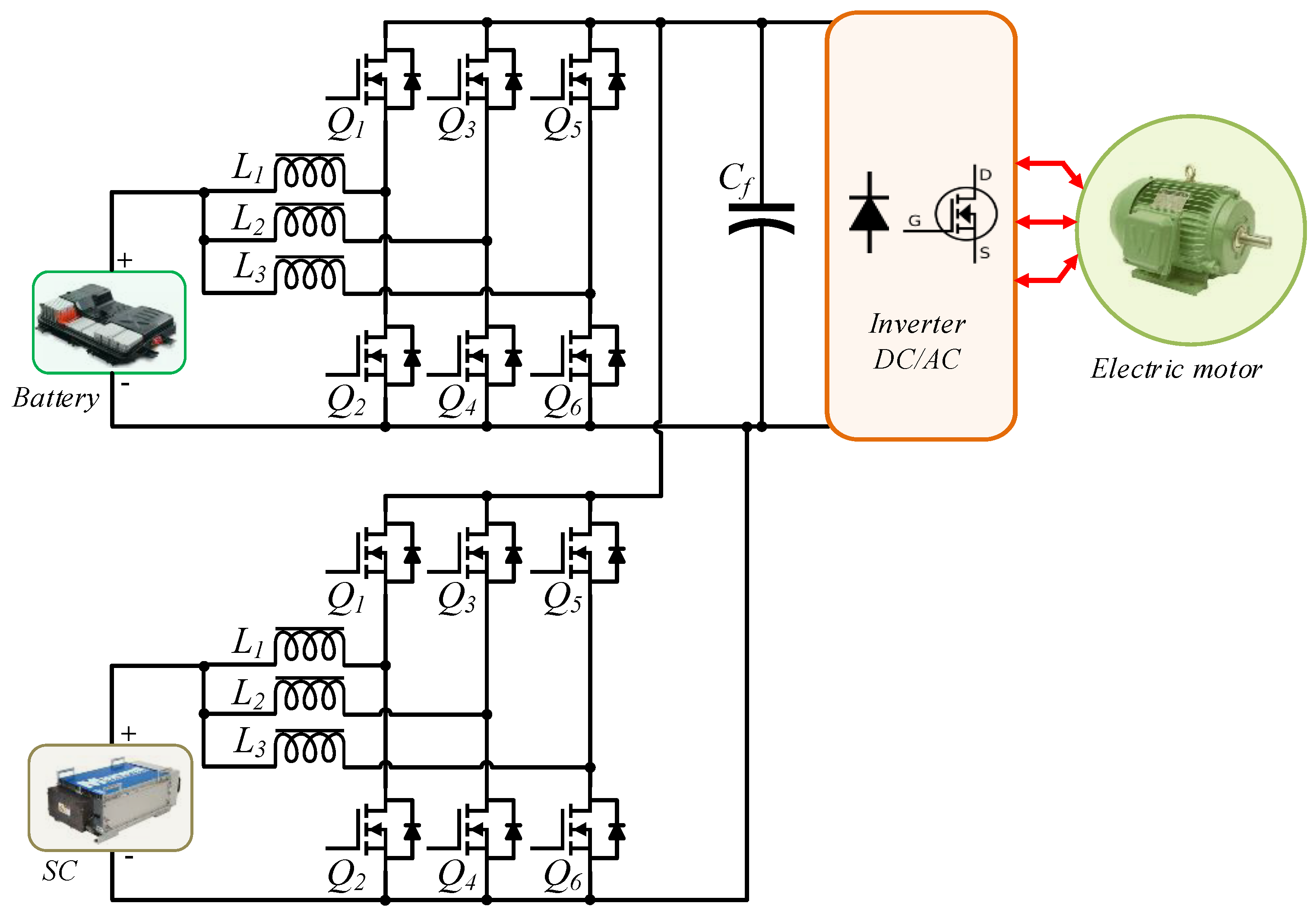
A family of MPCs is classified as non-isolated and isolated topology. In an isolated topology, the sources are usually connected to a half bridge converter to achieve DC-AC conversion, which allows the use of a high frequency transformer for high voltage ratios. In addition, the transformer enables the galvanic isolation between the inputs and outputs. Furthermore, with a transformer, it is easier to connect several outputs at different voltage level by properly selecting the number of turns of the secondary winding. However, for high power applications, the transformer is a bulky component. Thus, in vehicular applications, non-isolated topologies are preferred. Non-isolated MPC can be divided into parallel ports topologies and shared components topologies. The advantage of a shared component topology is that less switches are needed and thus the price is expected to be lower; however some topologies as presented in [2] are unable to deliver energy simultaneously. Parallel ports instead inherently increase the system reliability as the ports can be driven either simultaneously or independently, relying on different active components [3]. The advantage of paralleling the ports in a single converter is the gain in flexibility on the energy management techniques, compared to shared component. In fact, the ports can be controlled separately. In addition, better packaging and thermal management can be achieved compared to standard DC/DC converters. Despite being lighter compared to isolated converters, weight and cost is the main drawback in confront of shared components MPCs. Therefore, the interleaving technique can be applied to reduce the global converter weight and cost. Several MPCs have been developed based on [3] as in [4,5], proving a high efficient and compact solution for vehicle applications with a centralized control. Figure 2 shows a typical configuration of non-isolated bidirectional interleaved MPC in the vehicle powertrain.
The design of MPC power electronics system requires multidisciplinary knowledge and a large number of design variables in different engineering fields (electrical, magnetic, thermal, mechanical). The ability and expertise of the designer may end up with a good, but not optimal design. It may require more effort for further iterations through hardware prototype testing to obtain better performance in term of efficiency and weight. Therefore, mathematical optimization techniques and computer-aided software have been developed to tackle the design problem. In the literature, optimization for the power converter design can be classified into two main techniques: the gradient-based techniques using the derivative information and the metaheuristic-based techniques using the stochastic search. Several gradient-based methods have been employed for the optimization problem of power converter. Seeman et al. [6] used the Nonlinear Programming (NP) based on Lagrangian functions to optimize a switched-capacitor converter. Wu et al. [7] used the Augmented Lagrange Penalty Function (ALPF) technique to optimize a half-bridge dc-dc converter. Sergio et al. [8] utilized the Sequential Quadratic Programming (SQP) for a boost power-factor-correction converter optimization. However, the main drawback of gradient-based algorithms is that if the design space contains several local minima, there is a possibility that a gradient-based optimizer may be trapped by a local minimum, and the result depends on the selection of the initial design point. So far in the literature, no existing gradient-based algorithms are able to find the global optimization solution [9]. Furthermore, the gradient-based methods are mathematically guided algorithms, which require stringent mathematical formulations, causing a complexity of the system when variables increase. The metaheuristic-based optimization method was thus developed to solve the derivative-free and multi-objective problem with a large number of variables. Metaheuristic methods imitate the best features in nature, based on natural selection and social adaption. Among numerous metaheuristic methods, Genetic Algorithm (GA) [10] and Particle Swarm Optimization (PSO) [11] have been widely utilized to design the circuity of a power converter. The GA can be applied to optimize the medium-frequency transformer [12] of isolated converter, heatsink and bus capacitor volumes [13] of a three-phase inverter to archive minimum weight, losses and cost, with respect to constraints of design specification and physical limitation of components. The PSO, combined with Differential Evolution (DE), helps find an optimal transformer design for the Dual-Active-Bridge converter [14], the resonant tank of isolate bidirectional series resonant converter [15], and the inductor using EE core geometry [16]. So far, almost all researches have formulated a single objective formulation (efficiency, or weight, or cost [8]) or aggregated multiple conflicting objectives (weight, and loss, and cost) into one single objective. The multi-objective optimization of transformer design was solved by the Non-dominated Sorted Genetic Algorithm (NSGA-II) [12]; however, the final design selected from Pareto-solutions was not explained clearly.
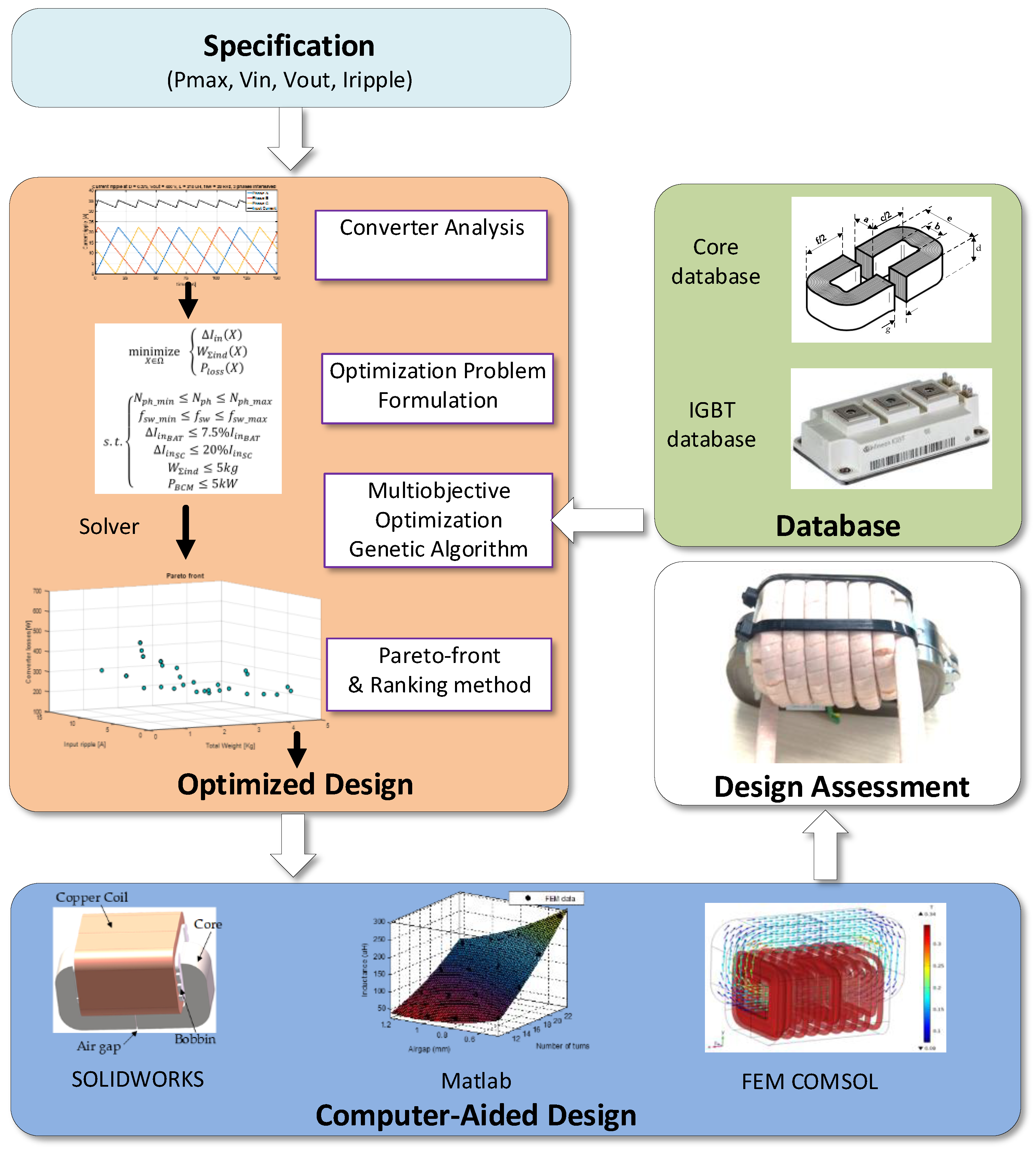
In this paper, a new optimization methodology as shown in Figure 3 is proposed for the non-isolated interleaved MPC. The main characteristics of the interleaved converter are analyzed by predefined specifications such as maximum power Pmax, input voltage Vin, output voltage Vout and required input current ripples Iripple for battery and Supercapacitor (SC) ports, to derive objective functions that can be used for optimization problem formulation. A multi-objective genetic algorithm and Average Ranking technique are then employed to find three design variables (the number of phases , switching frequency , and core index representing geometry parameters of the core) to simultaneously minimize three trade-off objectives: weight of inductors, converter losses and input current ripples. To closely attain a practical design, a database was developed, which included commercial available inductor cores (23 cores) and Insulated Gate Bipolar Transistor (IGBT) modules (8 IGBT modules) for the optimization process. A hypothesis is that an optimal solution can be found in the database. The SOLIDWORKS software (Solidworks Premium 2018, Dassault Systèmes SolidWorks Corporation, Waltham, MA, USA, 2018) is then used to visualize the physical structure of optimal inductors that are imported into the COMSOL Multiphysics (Version 5.3a, COMSOL, Inc., Burlington, MA, USA, 2018), a Finite Element Method (FEM)-based software, to simulate the electromagnetic field of the designed inductor. The curve fitting Matlab function is also used to plot the inductance value in the function of air-gap and number of turns. The simulation results show reduction of weight in the optimized design compared to a conventional design.
The organization of this paper includes six sections. Section 2 presents an analysis of input current ripple, weight of inductor, and converter losses. Section 3 formulates the multiple objectives optimization problem. Section 4 explains about the proposed design framework based on NSGA-II and Average Ranking method and Section 5 discusses improvement in the optimized design compared to the conventional design. The conclusions are given in Section 6.
2. Analysis of Non-Isolated Interleaved DC-DC Converter
As analyzed in the Introduction, isolated MPCs are usually used for low-power systems due to the limitation of magnetic designs for transformers. Non-isolated MPC topologies are more suitable for high-power powertrain system of vehicles. Thus, in this paper, the topology of MPC in Figure 2 has been selected for optimization. The MPC consists of two Interleaved Bidirectional Converters (IBC) interfacing with a battery port and SC port, respectively. The objective of design optimization is to minimize input current ripple, converter losses, and inductor weight of IBC for each port. Some key parameters are foreseen intuitively to have an impact on optimization objectives. Firstly, if the switching frequency increases, the size of the inductor core can be reduced; however, switching loss is increased. Secondly, the more number of phases added, the more current flowing in each phase can be reduced, leading to less semiconductor losses and reduction in inductor sizing. However, this adds more weight to the power electronics system. Finally, a bulky inductor can reduce the input current ripple that is important for battery lifespan; however, it introduces more weight and core losses. Therefore, the relationship of optimization objectives and design variables needs to be thoroughly analyzed.
2.1. Input Current Ripple
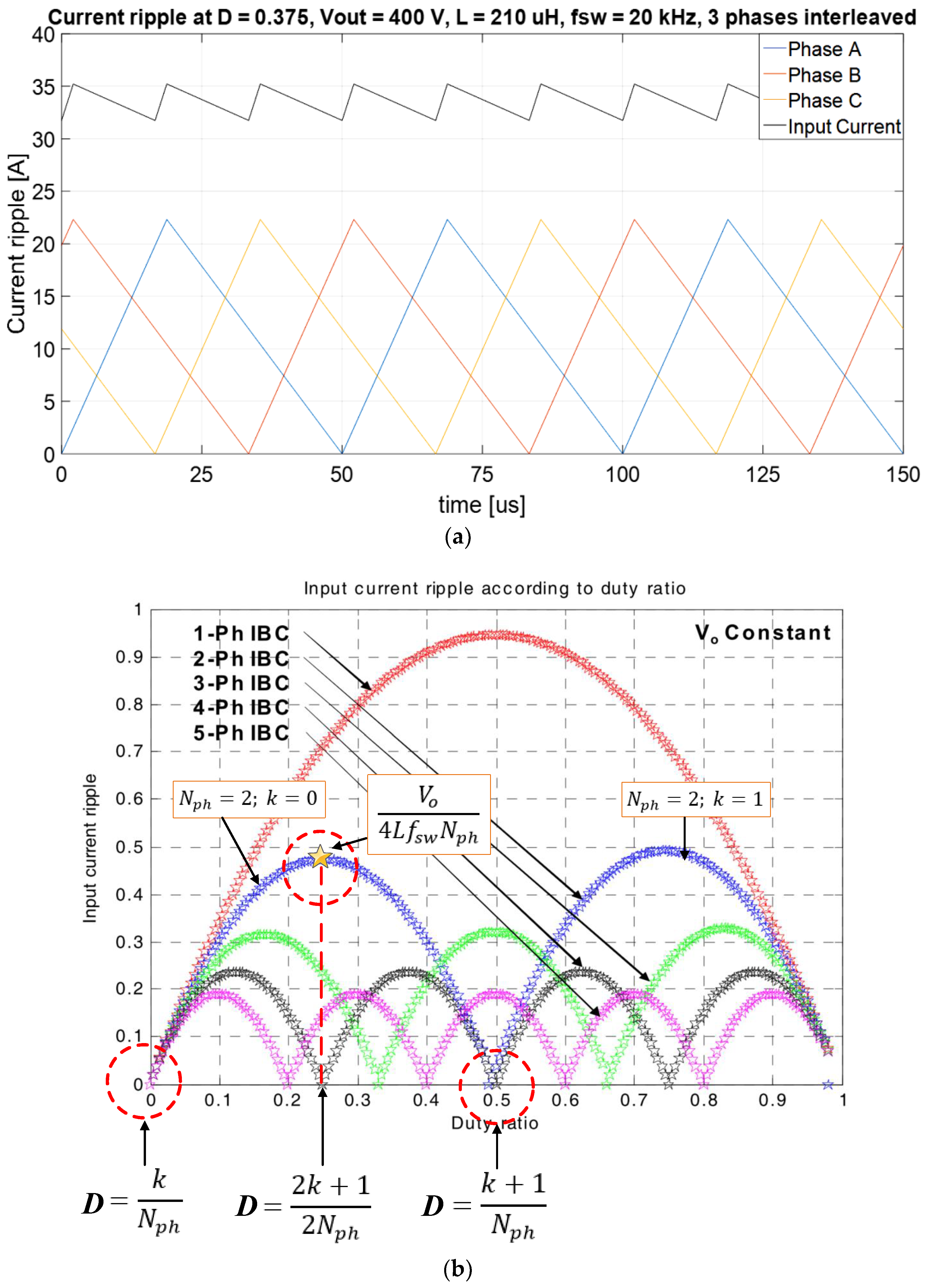
In the IBC, the phase interleaving technique enables one to decrease the input current ripple by shifting each interleaved phase by such that the current is cancelled out, as shown in Figure 4a. More phases are added in the interleaved converter; the peak is further reduced for each additional phase added. However, even though the amplitude of the ripples is reduced, the frequency of the ripples increases with increase in the number of phases.
The input current ripple cancellation effect of an interleaved converter in the Continuous Conduction Mode (CCM) has been analyzed and quantified in [17,18,19]. However, their derived equations are complicated to use in formulating the optimization problem. For the sake of convenience in the optimization process, we rewrite the function of input current ripple in terms of the duty ratio.
According to [17,18,19], the function of input current ripple with regard to the duty ratio can be recognized as a parabolic equation, , as shown in Figure 4b. As can be seen, if the IBC has phases, the peak of current ripple occurs separately in regions of duty ratio. Each region is associated with an integer number k ∈ [0, −1].
The vertex of the parabola and the points where is zero (dashed red circles in Figure 4b) are considered to determine the coefficients a, b and c. It is noted that the peak of the inductor current ripple in one single phase is calculated as Equation (1), therefore, the peak of the input current ripple becomes Equation (2):
As a result, the input current ripple analytical equation can be derived by the following system in Equation (3):
By solving the system, the analytical expression of is derived as Equations (4) and (5):
2.2. Weight of Inductors.
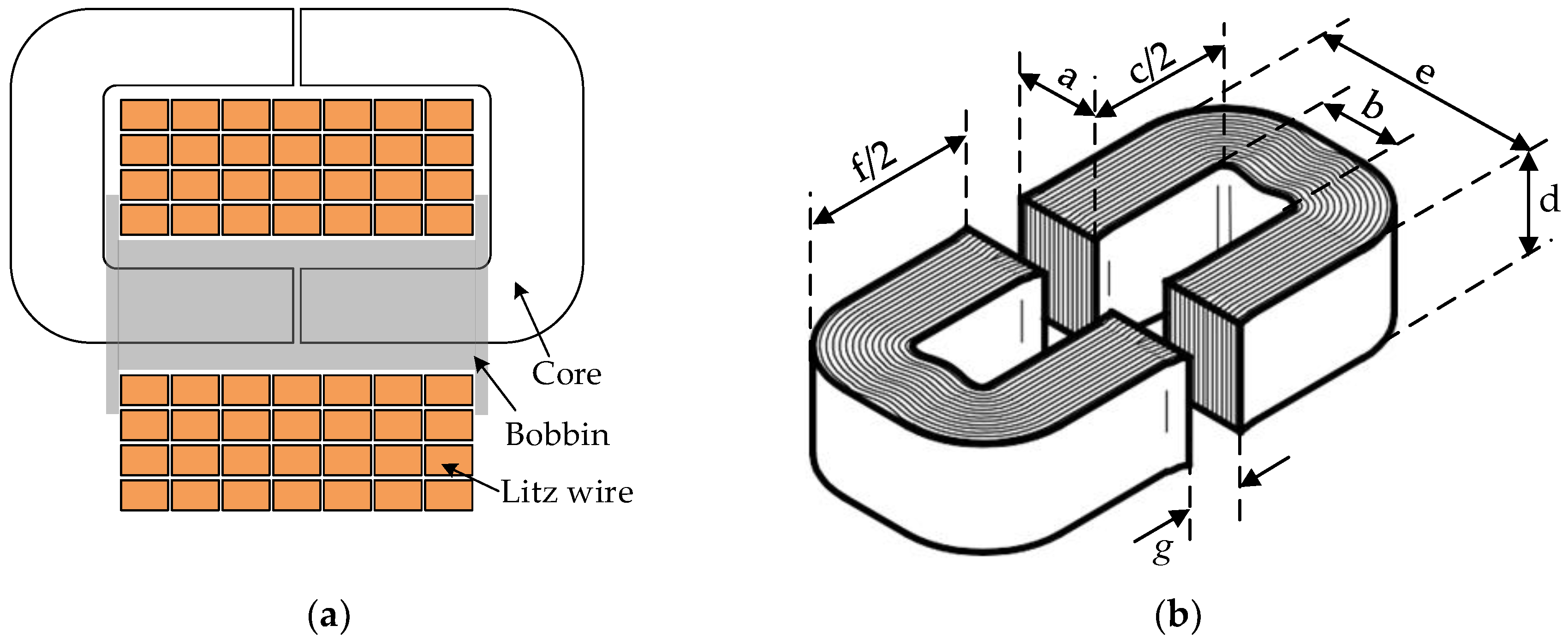
The weight of an inductor mainly consists of the weight of copper coil (or winding) and the weight of core. An inductor design is illustrated in Figure 5. The weight of a coil is dependent on the physical structure of winding (i.e., length, diameter, number of turns, and number of layers) while the weight of the core is dependent on the type of core (i.e., material, shape). The air gap is added to prevent saturation in the inductor.
To determine the weight of a coil , it is first necessary to calculate the number of turns as in Equation (6); (−) is utilization factor, is window area, is cross section of the wire:
The diameter of the wire conductor is calculated as Equation (7), where is current density:
which gives the number of layers as in Equation (8):
where the function returns the nearest integer less than or equal to X. And is the height window of the core as shown in Figure 5b.
The number of turns on each layer is then calculated as Equation (9):
where the function returns to the nearest integer with X.
TThe length of the coil as in Equation (10) is then based on the number of turns , the number of layers and the geometric parameters of the core ( and in Figure 5b).
The weight of the coil is finally calculated as in Equation (11), where is the mass density of copper:
For one port, the total weight of inductors is based on the number of inductors according to the number of phases , the weight of core , the weight of coil . (assumed that the weight of bobbin is constant):
The inductor design is not straightforward. In practical design, the core is selected from available commercial products and the wire is decided by the amplitude of the inductor current. For the sake of optimization, it is necessary to derive the dependence of the inductance value on the design specifications (i.e., input current, switching frequency, output voltage). The main idea is that the designed inductor should guarantee the pre-defined current ripple which is also dependent on the duty cycle and the switching frequency . In addition, the core of the inductor is not saturated. The inductance value can be derived from a second-degree polynomial equation as Equation (13). The detailed derivation steps are explained in the Appendix.
From Equation (13), it is possible to calculate the maximum inductance that can be achieved by a given core. It is obvious that out of the two roots of (13), only the real root has a physical meaning.
2.3. Losses of Converter
Losses of one phase consist of IGBT losses (conduction loss and switching loss), inductor losses (conduction loss and core loss) and air-gap loss. The loss caused by the skin effect can be neglected.
2.3.1. IGBT Losses and Diode Losses
The losses of IGBTs () and diodes () are due to the conduction losses and switching losses, which are evaluated based on [20], but neglecting the effect of the temperature variation.
where the IGBT and diode characteristics (, , , , , , , , IF and ) are given by the IGBT and diode datasheets; in addition, the effect of temperature variation is neglected. , , and are the switch and diode current.
2.3.2. Inductor Losses
The inductor losses consist of conduction loss , core loss , and air-gap loss . As shown in Equation (17), the conduction loss known as ohmic loss is dependent on the internal resistance of winding . The core loss as in Equation (18) are produced from the flux density ripple , which is proportional to the inductor current ripple . The core losses are estimated based on the charts given by the manufacturer (METGLAS, Inc., CC core) [21]. In addition, high-frequency gap loss in nanocrystalline cores [22] can be computed as in Equation (19).
where = 1.68 × 10⁻³ a numerical constant, c (mm): the depth of the iron core.
The total losses of interleaved converter for one port is calculated in Equation (20).
3. Optimization Problem Formulation
The optimization process aims at the optimal set of the inductor, the number of phases, and switching frequency to minimize three objective functions: the input current ripple ( as shown in Equation (4)), the total losses of the converter ( as shown in Equation (20)), and the weight of all inductors ( as shown in Equation (12)) that contributes critically to the whole weight of the converter. It is assumed that the weight of other components such as heat sink, IGBT modules, bus bar, and filter capacitor is fixed during the optimization process. The multi-objective optimization problem is mathematically presented in Equation (21).
The design vector containing three variables (continuous , discrete , and discontinuous Core index) must be found in the feasible solution space and subject to several constraints according to design specifications, physical limitation, and component safe operating areas. The minimum CCM power is added in the optimization routine to consider the negative effect of interleaving to ensure the Boundary Condition Mode (BCM) is at high power. In fact, as the current is split into several phases, the power at which the converter work in BCM is given by Equation (22):
4. NSGA-II Optimizer for the Proposed Optimization Design Framework
Figure 3 shows the flowchart of the proposed optimization framework based on Non-dominated Sorting Genetic Algorithm-II (NSGA-II) for the converter of individual ports in the MPC. The NSGA-II is the second version of the famous “Non-dominated Sorting Genetic Algorithm” based on the work of Prof. Kalyanmoy Deb et al., which solves non-convex and non-smooth single and multi-objective optimization problems. The detailed working principle of the NSGA-II can be found in [23]. The NSGA-II can achieve good performance while solving a type of multidimensional problem defined in Equation (21) with discontinuous variable, providing highly accurate results with a reduced number of evaluations. The design methodology uses the large database of commercial standard core and IGBT modules to guarantee a hypothesis that the optimal core can be found in the database.
The main principle of the NSGA-II is that each design solution is represented by its chromosome made of the different genes, where the genes represent the integer associated with the design variable; the new design solutions are then produced by reproduction of the parents (design choices). The Blend Crossover (BLX) during the reproduction is based on the arithmetical average of each gene and a random variable α. In addition, polynomial mutation is also considered to introduce diversity in the design choices.
Based on the principle of NSGA-II [23], in this research an existing Multi-Objective Genetic Algorithm (MOGA) has been modified. A built-in Matlab function called “gamultiobj” is used to create modified NSGA-II. In the Matlab setting “gaoptimset”, three primary functions are adapted: crossover operators (‘CrossoverFcn’), mutation operators (‘MutationFcn’) and the population selection of the next generation (‘CreationFcn’).
The presence of multiple objectives in a problem results in a set of Pareto-optimal solutions known as Pareto-front instead of a single optimal solution. A solution is called a Pareto-optimal solution if none of the objective functions can be improved in value without degrading some of the other objective values. Without any further information, one of these Pareto-optimal solutions cannot be said to be better than the other one, which demands a designer to find as many Pareto-optimal solutions as possible. Thus, the Average Ranking (AR) [24] is employed to underpin the final solution from the Pareto-front. In the AR method, the tensor is formulated as a three-dimensional matrix in Equation (23):
where is the objective function and is the design solution. records −1, 0 or 1 depending on whether the choice is better, equal to, or worse than on objective . The AR method calculates a score for each choice by summing the ranks of for each objective. For example, with 3 objectives, if is 2nd best on two of those objectives and 5th best on the other, its AR score will be 2 + 2 + 5 = 9. Therefore, for , where is the Pareto set as Equation (24):
The inner sum calculates a score for for a given objective, and this will be 1 if is the best on that objective. Generally, z + 1 if z members of P are better at that objective.
5. Optimization Results Assessment
To validate the proposed optimization framework, the optimized design and a conventional design are needed to satisfy the same specification as summarized in Table 1.
In the proposed optimization design, the upper bound and lower bound of design variables are defined in advance, as shown in Table 2. To be more detailed, the setting of NSGA-II parameters is shown in Table 3.
After executing the NSGA-II optimizer for the problem in Equation (21), the Pareto optimal solutions are sketched in Figure 6. The final optimal solution found by AR method shows that the optimal number of phases is three and optimal switching frequency is 60 kHz. The optimal core is AMCC50 from Metglas® Inc, a subsidiary of Hitachi Metals America, Ltd, Conway, SC, USA.
For the sake of a fair comparison, the switching frequency and number of phases, both found from the proposed methodology, are kept unchanged to design inductors in the conventional design that are based on well-established equations of a boost converter.
The inductance value of conventional design, as shown in Equation (25), should be sufficient to ensure the predefined input current ripple under the worst case (minimum input voltage ).
The selected core is AMCC50 with cross-section area , the maximum flux density . Without air gap, number of turns in the conventional design can be calculated by Equation (26).
The conventional and optimal design of inductors for battery and SC port are shown in Table 4. As can be seen, the inductance values increase from 166 (conventional design) to 177 (optimized design) for battery port, and from 148 (conventional design) to 150 (optimized design) for SC port even though the number of turns for both are reduced. The number of turns are reduced from 19 turns (conventional design) to 17 turns (optimized design) for the battery port, and from 18 turns (conventional design) to 15 turns (optimized design) for the SC port. It is understandable since the air-gaps 0.55 mm are added into the optimized inductor designs for two ports. As the results, the values of three objective functions are decreased considerably.
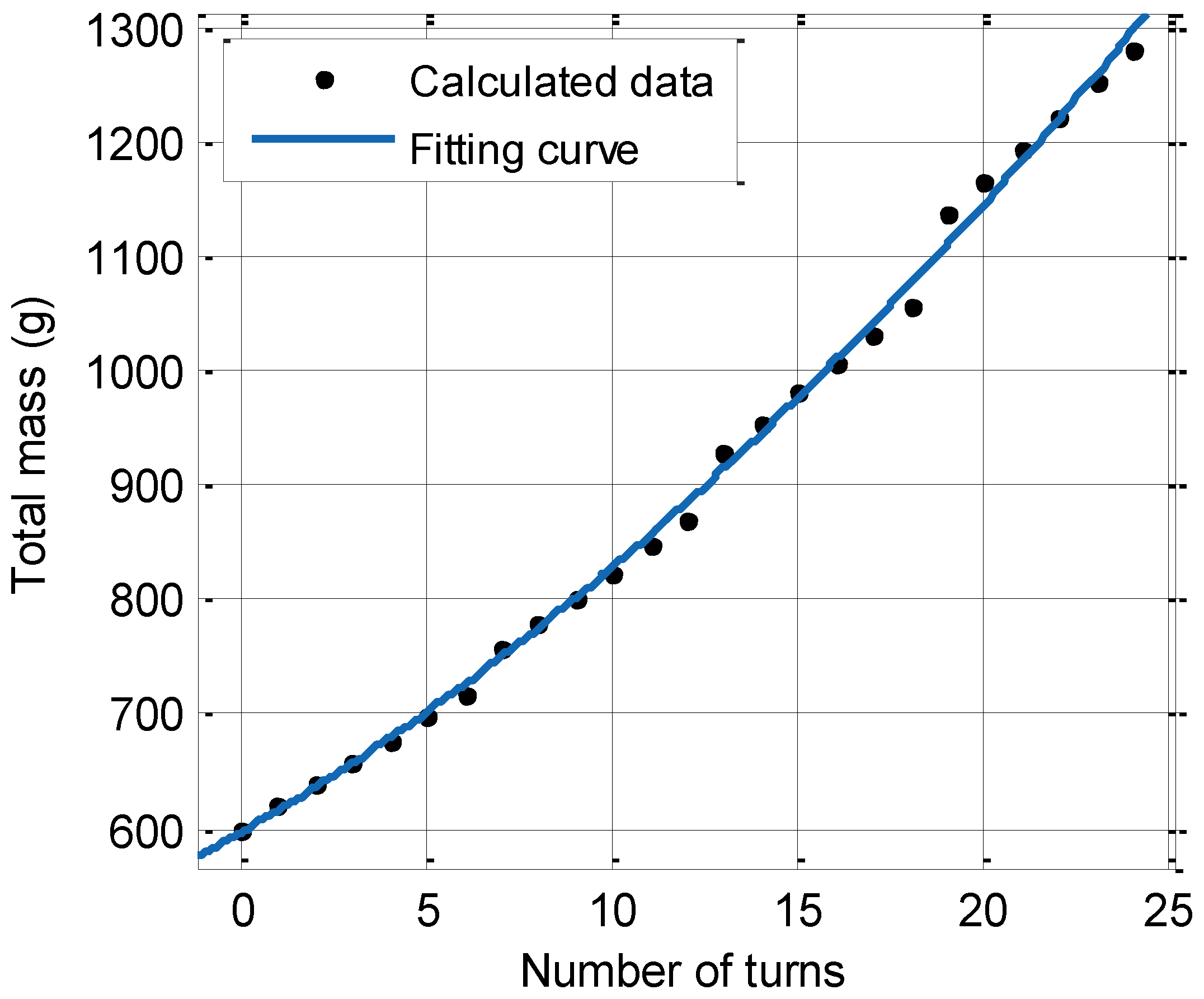
As shown before in Equation (12), the weight of the inductor consists of the weight of core, the weght of coil that is dependent on the length of wire, and the weight of the bobbin. The weight of AMCC50 core is 586 g and the weight of bobbin is 14 g. The Litz wire used for the wire of inductors is rectangular HF-LITZ WIRE covered with Polyester PET tape from Von Roll Isola France SA, Belfort, France, which has 0.2 kg/meter, 2600 strands, and the diameter of each strand is 0.1 mm. According to Equation (10), the length of wire for inductor coil can be calculated. Afterward, the weight of an inductor can be determined in a function of number of turns. For fast calculation, the relation between the weight of an inductor and the number of turns can be assumed as a 2nd-order polynomial curve that can be derived by using the fitting-curve function in Matlab as shown in Equation (27). Figure 7 illustrates the relation described in Equation (27). As can see from Table 4, the total weight of inductors is reduced by 20% and 17.6% for the battery port and the SC port, respectively.
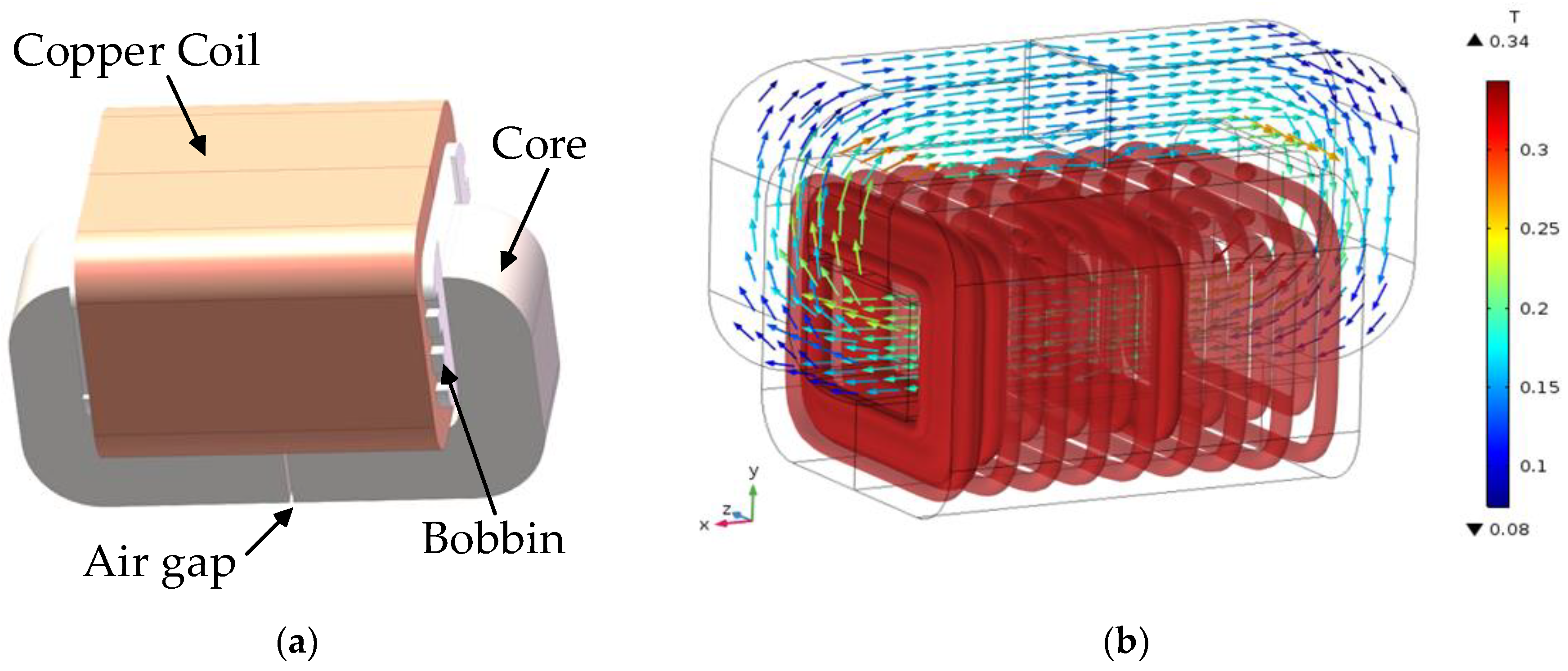
Since the input current ripple and converter losses are highly dependent on the inductance value, it is important to ensure that the real inductor can obtain value as close as possible to that of theoretical inductance. To fulfill this purpose, the commercial COMSOL Multiphysics software is employed to compute the model of the inductor based on Finite Element Method. Figure 8 illustrates the inductor design in SOLIDWORKS that is imported to the COMSOL software.
The material name of the core is METGLAS Alloy 2605SA1 that has high saturation flux density (1.56T) and a low loss resulting from micro-thin Metglas ribbon (25 ). To ease the computation time, the fitting technique is also used to find the inductance value in a function of air-gaps and number of turns. To do so, 16 inductance values are generated from COMSOL Multiphysics with air-gap range from 0–1.2 mm and number of turns from 10–22 turns. Using Matlab fitting function, a 2nd-order polynomial surface can be found as Equation (28).
where is inductance (µH); is airgap (mm). The impact of air gap and number of turns is simulated by FEM. The result is fitted by 2-degree polynomial function, mentioned as above. Figure 9 illustrates the impact of air-gap and the number of turns on the inductance value.
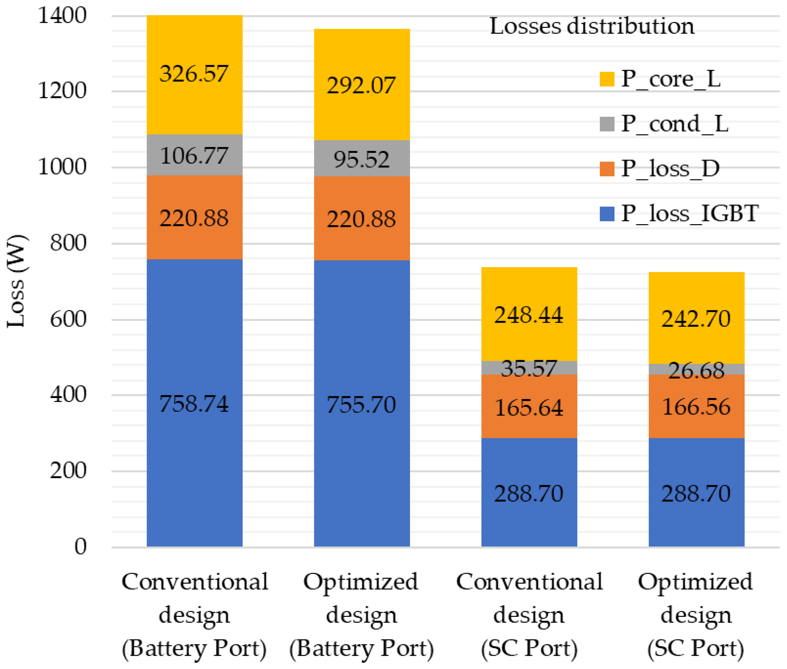
To calculate the reduction of losses, the SiC-based semiconductor switch (2MBI150U2A-060) is used and switching frequency is kept as 60 kHz. The power losses of converters at full load 30 kW are reduced by 3.5% and 2.02% for battery port and SC port, respectively. More reduction of total loss, 7.2% and 2.56% for battery and SC port respectively, can be seen at low load 5 kW. The losses distribution at full load is shown in detail in Figure 10.
The maximum input current ripple current, which is considered as a third objective function is also reduced by 38% and 34% for battery and SC converter ports, respectively. All diminution values that are shown in Table 4 validate the optimization methodology based on a multi-objective genetic algorithm and Average Ranking technique.
6. Conclusions
Several MPC topologies have been proposed in recent years with the aim to decrease the weight and component counts of DC/DC converters applied in hybrid drivetrain systems. Thus, the complex multidisciplinary design of these converters is a key challenge in the development phase of vehicle or machine drivetrains.
In this paper, a new optimization methodology based on Nondominated Sorting Genetic-Algorithm-II has been developed for MPC design to find optimization variables: a number of phases, inductor design, and switching frequency. The Average Ranking method is proposed to finalize the optimal solution among several Pareto-front solutions. Theoretically, the optimized design can archive better performance than the conventional design in terms of weight of inductors, input current ripple, and converter losses. The Finite Element Method such as COMSOL software is used to validate inductor designs, which is a crucial step for the future work. The proposed optimization process opens up new possible configurations in the optimization of MPC. Future research will involve the development of high-fidelity models of inductor design considering fringing effects, and fabrication of the prototype of MPC to validate design methodology compared to conventional design.
Author Contributions
D.T. has written the manuscript and presented the optimization methodology; S.C. analyzed multiport converter; Y.L. designed and analyzed the inductors by COMSOL and SOLIDWORK, J.v.M. and O.H. reviewed and edited the manuscript and they also provided supervision guidance to this research.
Funding
This research was funded by EMTECHNO project (Emerging Technologies in Multiport Systems for Energy Efficient Drivetrains), grant number IWT150513.
Acknowledgments
We acknowledge Flanders Make and VLAIO for the support to our research group.
Conflicts of Interest
The authors declare no conflict of interest.
Appendix A
This Appendix section explains how to derive the Equation (13) in which the inductance value can be found from a given core and design specification. Main steps are highlighted as following.
Appendix A.1. Maximum Flux Density
The reluctance of the core can be neglected compared to the one of the air gap results in Equation (A1):
where is the number of turns, the magnetic flux, the air gap, the vacuum magnetic permeability and the net cross-sectional area of the core.
Given a peak winding current , it is desired to operate the core flux density at a peak value below the saturation flux density . Therefore:
Appendix A.2. Inductance
The inductance is related to the number of turns and the reluctance.
Appendix A.3. Winding Area
The wire must fit through the core window . However, the wire does not pack perfectly which reduces the utilization factor of the core window. Furthermore, insulation and the bobbin itself take some other place causing the utilization factor to drop to values between 0.3 and 0.6. As a result, the number of turns in the core is limited by Equation (A4).
where is the conductor cross section.
Appendix A.4. Conductor Cross Section
The conductor needs to carry the peak current; therefore, another constraint is as Equation (A5):
By substituting Equation (A5) into Equation (A4) and then into Equation (A2) an expression of the maximum air-gap for the maximum number of turns can be derived in Equation (A6):
It is clear that is a function of only the material and geometry of the core and it expresses the needed air gap to avoid that the material saturates when the core window is filled with conductors. In standard design techniques, is calculated by the specifications on the . However, in this design algorithm, is a design variable, while the specification is set to which can be met with the phase interleaving. As a result, becomes a design variable and it is related to the selected core. Moreover, it is worth expressing the peak current explicitly in terms of the inductance . Therefore, as Equation (A7):
where in the interleaved case is as Equation (A8):
By substituting (A7) and a version of Equation (A1) rearranged in into Equation (A2) a second-degree polynomial expression of can be derived.
References
- Chan, C.C.; Bouscayrol, A.; Chen, K. Electric, Hybrid, and Fuel-Cell Vehicles: Architectures and Modeling. IEEE Trans. Veh. Technol. 2010, 59, 589–598. [Google Scholar] [CrossRef]
- Dobbs, B.G.; Chapman, P.L. A multiple-input DC-DC converter topology. IEEE Power Electron. Lett. 2003, 1, 6–9. [Google Scholar] [CrossRef]
- Solero, L.; Lidozzi, A.; Pomilio, J.A. Design of Multiple-Input Power Converter for Hybrid Vehicles. IEEE Trans. Power Electron. 2005, 20, 1007–1016. [Google Scholar] [CrossRef]
- Jiang, W.; Fahimi, B. Multiport Power Electronic Interface—Concept, Modeling, and Design. IEEE Trans. Power Electron. 2011, 26, 1890–1900. [Google Scholar] [CrossRef]
- Hegazy, O.M.; Baghdadi, E.; Van Mierlo, J.; Lataire, P.; Coosemans, T. Analysis and modeling of a bidirectional multiport DC/DC power converter for battery electric vehicle applications. In Proceedings of the 2014 16th European Conference on Power Electronics and Applications, Lappeenranta, Finland, 26–28 August 2014. [Google Scholar]
- Seeman, M.D.; Sanders, S.R. Analysis and Optimization of Switched-Capacitor DC–DC Converters. IEEE Trans. Power Electron. 2008, 23, 841–851. [Google Scholar] [CrossRef]
- Wu, C.J.; Lee, F.C.; Balachandran, S.; Goin, H.L. Design Optimization for a Half-Bridge DC-DC Converter. IEEE Trans. Aerosp. Electron. Syst. 1982, 4, 497–508. [Google Scholar] [CrossRef]
- Busquets-Monge, S.; Crebier, J.C.; Ragon, S.; Hertz, E.; Boroyevich, D.; Gurdal, Z.; Arpilliere, M.; Lindner, D.K. Design of a boost power factor correction converter using optimization techniques. IEEE Trans. Power Electron. 2004, 19, 1388–1396. [Google Scholar] [CrossRef]
- De Leon-Aldaco, S.E.; Calleja, H.; Aguayo Alquicira, J. Metaheuristic Optimization Methods Applied to Power Converters: A Review. IEEE Trans. Power Electron. 2015, 30, 6791–6803. [Google Scholar] [CrossRef]
- Man, K.F.; Tang, K.S.; Kwong, S. Genetic algorithms: Concepts and applications [in engineering design]. IEEE Trans. Ind. Electron. 1996, 43, 519–534. [Google Scholar] [CrossRef]
- Kennedy, J.; Eberhart, R. Particle swarm optimization. In Proceedings of the ICNN’95-International Conference on Neural Networks, Perth, WA, Australia, 27 November–1 December 1995. [Google Scholar]
- Garcia-Bediaga, A.; Villar, I.; Rujas, A.; Mir, L.; Rufer, A. Multiobjective Optimization of Medium-Frequency Transformers for Isolated Soft-Switching Converters Using a Genetic Algorithm. IEEE Trans. Power Electron. 2017, 32, 2995–3006. [Google Scholar] [CrossRef]
- Ledoux, C.; Lefranc, P.; Larouci, C. Pre-sizing optimization of an inverter and the passive components. In Proceedings of the 2011 14th European Conference on Power Electronics and Applications, Birmingham, UK, 30 August–1 September 2011. [Google Scholar]
- Qin, H.; Kimball, J.W.; Venayagamoorthy, G.K. Particle swarm optimization of high-frequency transformer. In Proceedings of the IECON 2010-36th Annual Conference on IEEE Industrial Electronics Society, Glendale, AZ, USA, 7–10 November 2010. [Google Scholar]
- Kundu, U.; Sikder, S.; Kumar, A.; Sensarma, P. Frequency domain analysis and design of isolated bidirectional series resonant Dc-dc converter. In Proceedings of the 2016 IEEE International Conference on Power Electronics, Drives and Energy Systems (PEDES), Trivandrum, India, 14–17 December 2016. [Google Scholar]
- Mirjafari, M.; Balog, R.S. Multi-objective design optimization of renewable energy system inverters using a Descriptive language for the components. In Proceedings of the 2011 Twenty-Sixth Annual IEEE Applied Power Electronics Conference and Exposition (APEC), Fort Worth, TX, USA, 6–11 March 2011. [Google Scholar]
- Zhang, S. Analysis and minimization of the input current ripple of Interleaved Boost Converter. In Proceedings of the 2012 Twenty-Seventh Annual IEEE Applied Power Electronics Conference and Exposition (APEC), Fort Worth, TX, USA, 6–11 March, 5–9 February 2012. [Google Scholar]
- Choe, G.-Y.; Kim, J.-S.; Kang, H.-S.; Lee, B.-K. An Optimal Design Methodology of an Interleaved Boost Converter for Fuel Cell Applications. J. Electr. Eng. Technol. 2010, 5, 319–328. [Google Scholar] [CrossRef] [Green Version]
- High Efficiency, High Density, PolyPhase Converters for High Current Applications. Available online: http://bee.mif.pg.gda.pl/ciasteczkowypotwor/Noty%20aplikacyjne/Linear%20Technology/an77f.pdf (accessed on 26 July 2018).
- Determining Switching Losses of SEMIKRON IGBT Modules. Available online: https://www.semikron.com/dl/service-support/downloads/download/semikron-application-note-switchinglosses-en-2014-08-19-rev-00/ (accessed on 26 July 2018).
- Metglas, Inc. Inductor Cores, Powerlite Technical Bulletin. Available online: http://www.metglas.com (accessed on 26 July 2018).
- Wang, Y.; Calderon-Lopez, G.; Forsyth, A.J. High-Frequency Gap Losses in Nanocrystalline Cores. IEEE Trans. Power Electron. 2017, 32, 4683–4690. [Google Scholar] [CrossRef]
- Deb, K.; Pratap, A.; Agarwal, S.; Meyarivan, T. A fast and elitist multiobjective genetic algorithm: NSGA-II. IEEE Trans. Evol. Comput. 2002, 6, 182–197. [Google Scholar] [CrossRef] [Green Version]
- Corne, D.W.; Knowles, J.D. Techniques for highly multiobjective optimisation. In Proceedings of the 9th annual Genetic and Evolutionary Computation Conference, London, UK, 7–11 July 2007. [Google Scholar]
Figure 1.
Multiport Converter integrated into the EVT-based powertrain.
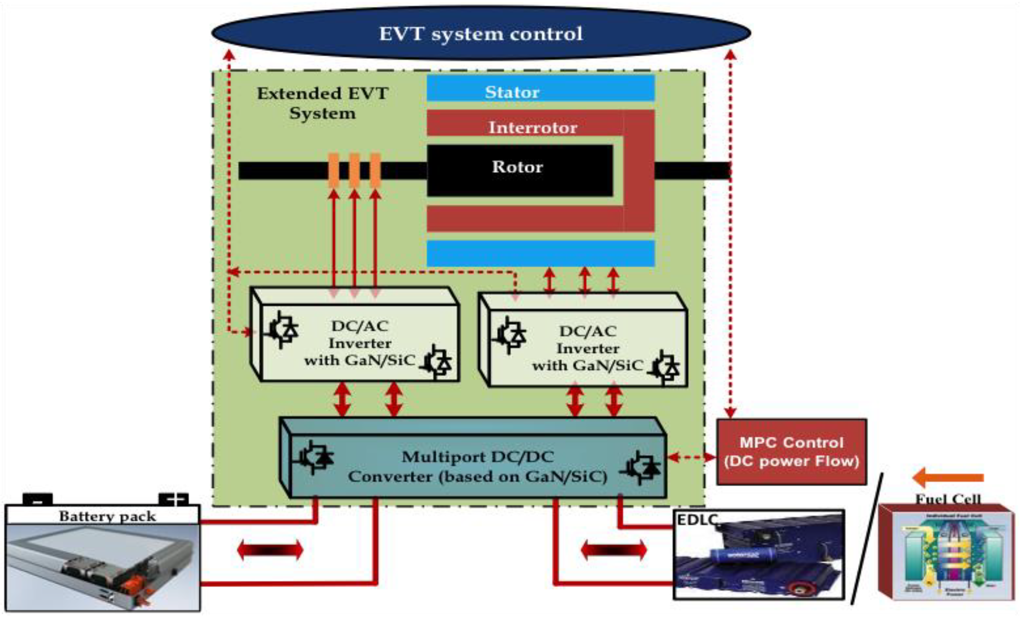
Figure 2.
Non-isolated MPC using an interleaved bidirectional converter for each port in the Full Electric Bus powertrain.
Figure 2.
Non-isolated MPC using an interleaved bidirectional converter for each port in the Full Electric Bus powertrain.

Figure 3.
Proposed design optimization methodology.

Figure 4.
(a) Reduction of input current ripple through phase interleaving. (b) Normalized peak-to-peak input current ripple as a function of the duty ratio.
Figure 4.
(a) Reduction of input current ripple through phase interleaving. (b) Normalized peak-to-peak input current ripple as a function of the duty ratio.

Figure 5.
(a) Structure of an inductor; (b) Geometry parameters of a core.

Figure 6.
A three-dimensional Pareto optimal solution.
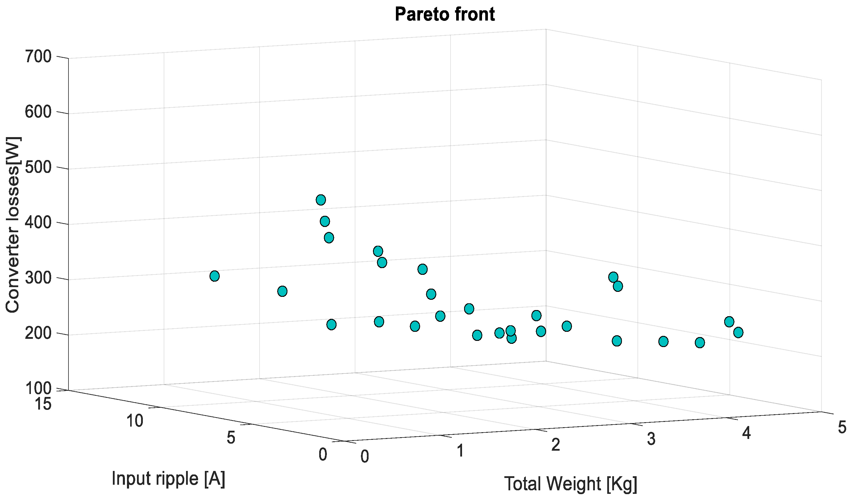
Figure 7.
Weight of an inductor in function of number of turns.

Figure 8.
(a) SOLIDWORKS inductor design, (b) Magnetic flux distribution and current distribution of inductor in the COMSOL Multiphysics (Version 5.3a, COMSOL, Inc., Burlington, MA, USA, 2018).
Figure 8.
(a) SOLIDWORKS inductor design, (b) Magnetic flux distribution and current distribution of inductor in the COMSOL Multiphysics (Version 5.3a, COMSOL, Inc., Burlington, MA, USA, 2018).

Figure 9.
Inductance value in function of air-gap and number of turns.
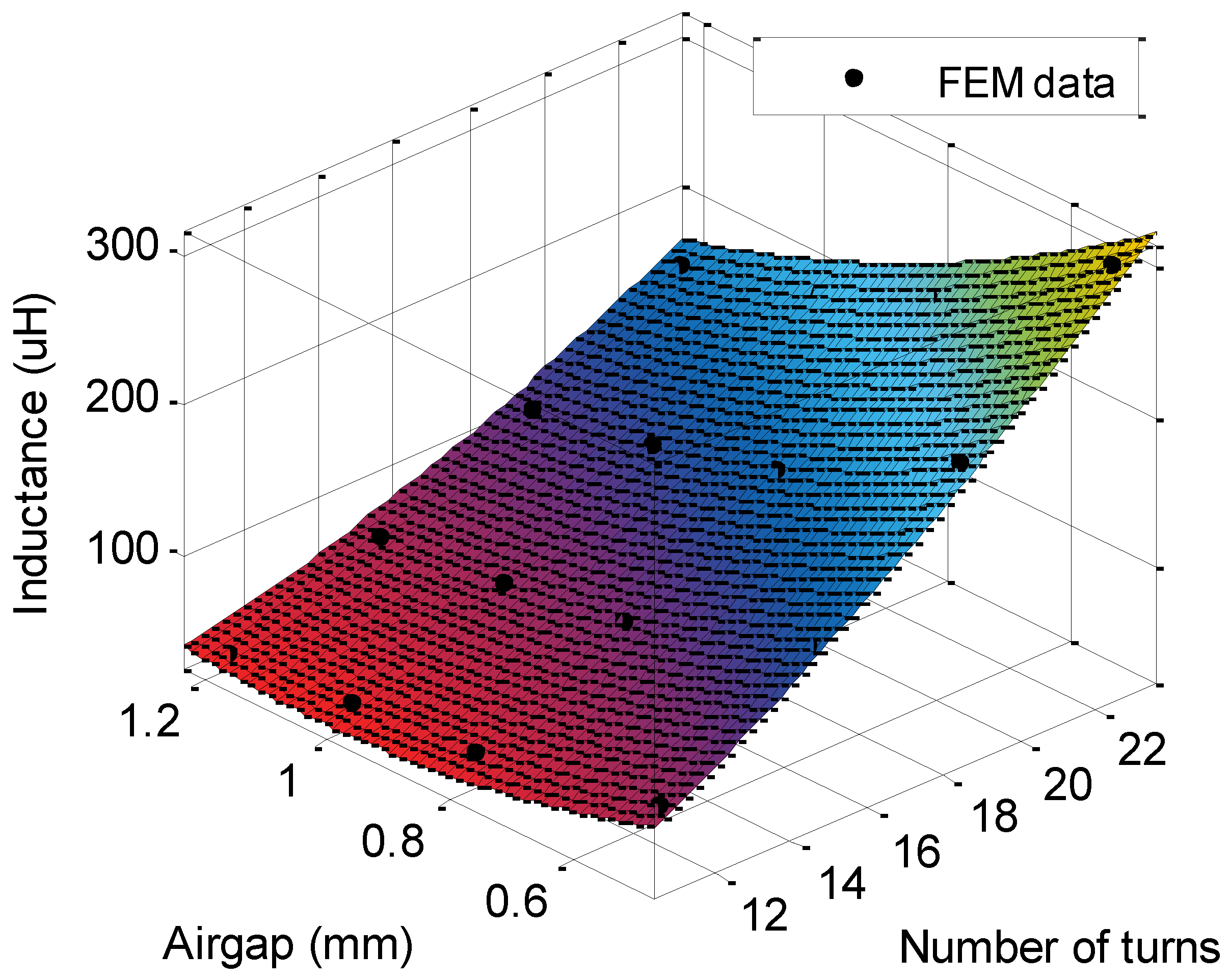
Figure 10.
Losses distribution comparison at full load 30 kW.

Table 1.
Design specification for MPC.
| Notation | Description | Unit | Battery Port | SC Port |
|---|---|---|---|---|
| Rating power | kW | 30 | ||
| Number of phases | [−] | 3 | ||
| Output voltage | V | 400 | ||
| Maximum input voltage | V | 250 | 400 | |
| Minimum input voltage | V | 200 | 200 | |
| Input current | A | 150 | 166.67 | |
| Input ripple current | A | 15 | 16.67 | |
| Input peak current | A | 157.5 | 175 | |
| Minimum output current | A | 5 | ||
Table 2.
Design variable bounds.
| Design Variables | Symbol | Lower Bound | Upper Bound | Unit |
|---|---|---|---|---|
| Number of phases | 2 | 4 | − | |
| Switching frequency | 20 | 100 | kHz | |
| Core database | 23 | |||
Table 3.
Parameter settings used in GA.
| Parameters | Value |
|---|---|
| Generation number | 200 |
| Population size | 50 |
| Crossover probability | 0.85 |
| Mutation probability | 0.1 |
Table 4.
Comparison between the conventional and optimized design for Battery and SC ports.
| Notation & Description | Unit | Battery Port | SC Port | |||||
|---|---|---|---|---|---|---|---|---|
| Conventional | Optimized | Conventional | Optimized | |||||
| Inductance | 166 | 177 | - | 148 | 150 | - | ||
| Number of turns for inductor | turns | 19 | 17 | - | 18 | 15 | - | |
| Air gap for inductor core | mm | 0 | 0.55 | - | 0 | 0.55 | - | |
| Weight of inductors for 3 phases | kg | 3.41 | 2.73 | 20% | 3.17 | 2.61 | 17.6% | |
| Power losses of converter at full load (30 kW) | kW | 1.41 | 1.36 | 3.5% | 0.74 | 0.72 | 2.02% | |
| Power losses of converter at low load (5 kW) | kW | 0.55 | 0.51 | 7.2% | 0.39 | 0.38 | 2.56% | |
| Maximum input current ripple | A | 15 | 9.32 | 38% | 16.67 | 11 | 34% | |
© 2018 by the authors. Licensee MDPI, Basel, Switzerland. This article is an open access article distributed under the terms and conditions of the Creative Commons Attribution (CC BY) license (http://creativecommons.org/licenses/by/4.0/).
Share and Cite
MDPI and ACS Style
Tran, D.; Chakraborty, S.; Lan, Y.; Van Mierlo, J.; Hegazy, O. Optimized Multiport DC/DC Converter for Vehicle Drivetrains: Topology and Design Optimization. Appl. Sci. 2018, 8, 1351. https://doi.org/10.3390/app8081351
AMA Style
Tran D, Chakraborty S, Lan Y, Van Mierlo J, Hegazy O. Optimized Multiport DC/DC Converter for Vehicle Drivetrains: Topology and Design Optimization. Applied Sciences. 2018; 8(8):1351. https://doi.org/10.3390/app8081351
Chicago/Turabian StyleTran, Duong, Sajib Chakraborty, Yuanfeng Lan, Joeri Van Mierlo, and Omar Hegazy. 2018. "Optimized Multiport DC/DC Converter for Vehicle Drivetrains: Topology and Design Optimization" Applied Sciences 8, no. 8: 1351. https://doi.org/10.3390/app8081351
Note that from the first issue of 2016, this journal uses article numbers instead of page numbers. See further details here.