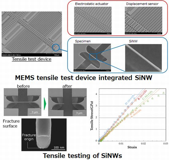
Tensile Strength of Silicon Nanowires Batch-Fabricated into Electrostatic MEMS Testing Device


Department of Micro Engineering, Kyoto University, Kyoto 615-8540, Japan
*
Author to whom correspondence should be addressed.
Appl. Sci. 2018, 8(6), 880; https://doi.org/10.3390/app8060880
Submission received: 20 April 2018
/
Revised: 16 May 2018
/
Accepted: 19 May 2018
/
Published: 28 May 2018
(This article belongs to the Special Issue Silicon Nanowires and Their Applications)
Abstract
:Featured Application
Piezoresistive sensors, Torsional mirrors.
Abstract
The tensile strength of a silicon nanowire (SiNW) that had been integrated into a silicon-on-insulator (SOI)-based microelectromechanical system (MEMS) device was measured using electrostatic actuation and sensing. SiNWs of about 150 nm diameter and 5 μm length were batch-fabricated into a 5-μm-thick SOI device layer. Since there was no interface between the SiNW and the MEMS device and the alignment was perfect, the SiNW integration into an SOI-MEMS was expected to be useful for developing highly sensitive biochemical sensors or highly reliable torsional mirror devices. The SiNW was tensile tested using the electrostatic MEMS testing device. The integration was achieved using a combination of anisotropic and an isotropic dry etching of silicon, with an inductively coupled plasma reactive ion etching. A fabricated silicon beam of 800 nm square was thinned by a sacrificial oxidation process. The tensile strength of the wire was 2.6–4.1 GPa, which was comparable to that of microscale silicon MEMS structures. The reliability of such a thin device was successfully verified for future applications of the device structures.

1. Introduction
Micro-electro-mechanical systems (MEMS), which are devices with electrical circuits, mechanical components, and electro-mechanical transducers, are now widely employed in various electrical systems, including those in automobile, portable, amusement, environmental, or infrastructure monitoring systems. The mechanical components in the conventional MEMS devices are only micrometers in scale and are based on well-developed semiconductor microfabrication technologies. Recently, for further miniaturization, higher performance, and more functionality, the integration of nanoscale components into MEMS has been widely investigated. These are referred to as nano-electro-mechanical systems (NEMS). The nano-carbons (graphene [1,2], carbon nanotubes [3,4], and fullerene [5]), biomolecules (proteins [6], lipids [7,8], and nucleic acids [9,10]), and metal nanoparticles [11,12] are examples of nanoscale components that have been integrated into MEMS or microfluidic devices. They provide a new functionality, better sensitivity, and higher reliability. However, there continues to be problems with the mechanical and electrical interfaces in their integration with the microscale structures in MEMS devices.
Silicon nanowire (SiNW) is also a candidate as a nanoscale component for mechanical or chemical sensing [13,14,15,16,17,18,19]. The piezoresistive strain gauge performs better when the dimensions are reduced [16,17]. The higher surface-to-volume ratio provides a higher sensitivity to chemical and biological sensing, which works as a molecular-sensitive field effect transistor [18,19]. One of the merits of using silicon is its well-developed fabrication technology. We can easily fabricate a nanowire on the substrate using nanoscale lithography and etching technology. However, creating a freestanding nanowire on a device is still a challenge. The pick-and-place technique was employed for the characterization of free-standing SiNWs fabricated using focused-ion-beam (FIB) processing [20,21], however it is not compatible with large-scale fabrication. Local chemical vapor deposition (CVD) growth has been used, but it requires an additional structure for heating and may not be compatible with the device structures [18,22]. Multi-step deposition and etching with wafer bonding has also been developed. The integration of MEMS and SiNW, using batch fabrication, has been achieved, however the fabrication process is costly [19]. An integration process that uses a simple silicon-on-insulator (SOI) wafer and standard process machines (deep reactive ion etching [DRIE]) is needed for low-cost fabrication to be realized.
In this research, we have proposed a fabrication process for a free standing SiNW on a SOI wafer, in which a SiNW of a few hundred micrometers in diameter is integrated into a device layer of 5 micrometers thickness. In the same device layer, the electrostatic transducers, which are responsible for force actuation and displacement sensing, and for the mechanical components such as the mass and springs, are integrated. The advantages of this process are as follows:
- No interface between a MEMS device structure and a SiNW;
- Perfect alignment; and
- Free from a complicated and time-consuming assembly process.
For a technical demonstration and material properties characterization, a MEMS tensile testing device for a SiNW of 100 nm thickness was fabricated and the tensile strength was measured in this research.
2. MEMS Tensile Testing Device with SiNW
A MEMS device for the tensile testing of SiNW was designed based on the device for a fullerene thin film [5]. We set the target diameter at 100 nm, and the tensile force that was required for the testing was estimated to be 30 μN, by assuming the tensile strength was 3 GPa. Upon performing a tensile test, the parallel plate actuator on the top was actuated to apply a tensile load on the specimen. The tensile force on the specimen was calculated by subtracting the restoring force of the supporting beams from the electrostatic force that was generated by the parallel plate actuator. The force was much higher than in our previous work, so we changed the electrostatic actuator from a comb drive type to a parallel plate type, which generated a larger force. The capacitive displacement sensor was used for the elongation measurement. The moving parts of both the actuator and sensor were supported by four folded beams and three o-shaped beams, and they were connected to the moving end of the SiNW. The schematic diagram and mask design of the device are shown in Figure 1 and the detailed design is presented in the Supplementary Materials.
3. Fabrication
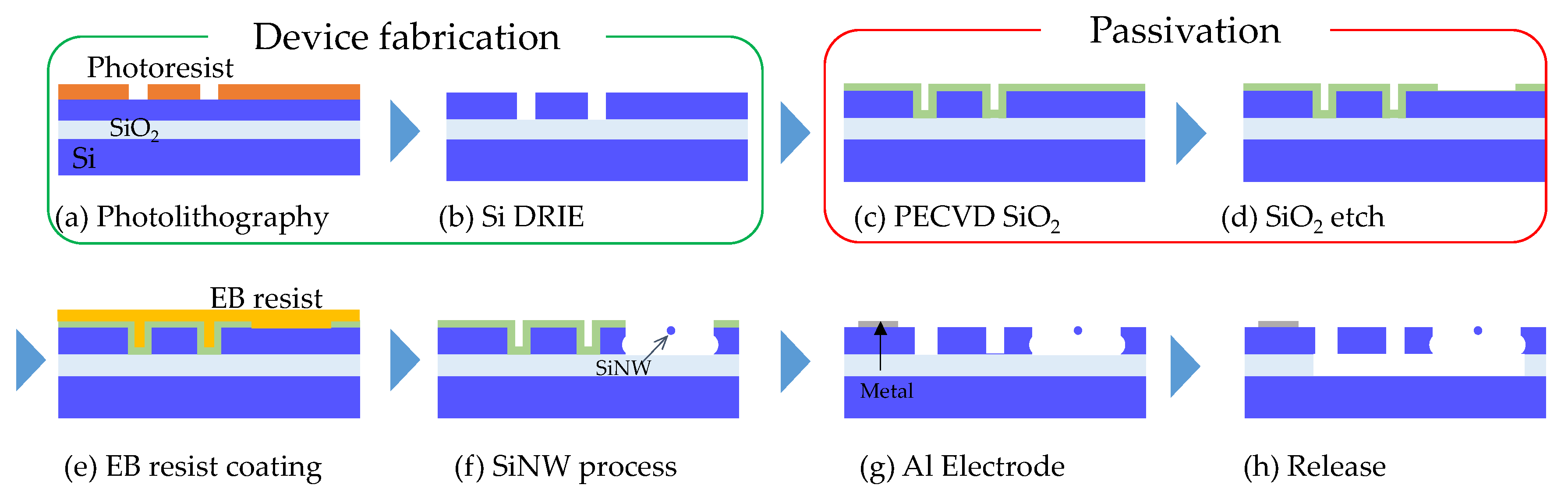
The key point of the fabrication process was the integration of the SiNW fabrication steps into the SOI-MEMS fabrication steps. As we employed an oxidation process to thin the SiNW in this research, we should have deposited the metal pads after the thinning process. However, it was difficult to keep the SiNW intact during the fabrication of the tensile testing structure. We started with the testing device fabrication first, except for the pad formation, as well as a sacrificial release. After the nanowire fabrication and thinning, aluminum pads were deposited using a stencil mask. The schematic diagram of the fabrication process is given in Figure 2.
3.1. Device Structure
The process was started with a 4 inch SOI wafer, whose device layer was a 5 μm thick p-type, heavily boron-doped silicon. The MEMS device structures were patterned with a photoresist (OFPR-800LB, Tokyo-Ohka, Kawasaki, Japan) using a contact photolithography tool (PEM-800, Union Optics, Tokyo, Japan). The device layer was etched using DRIE with the Bosch process (RIE-800iPB, Samco, Kyoto, Japan). After the resist removal, an oxide layer of 600 nm was deposited using a plasma enhanced chemical vapor deposition (PECVD) (MPX-CVD, SPP Technologies, Tokyo, Japan). The oxide layer was used to protect the electrostatic tensile test device structure from oxidation, therefore, the oxide was removed at the area where the SiNWs were fabricated. Then, the wafer was diced into 7 mm square chips using a blade dicer (DAD322, Disco, Tokyo, Japan). After the fabrication of the SiNW with the chips, a 600 nm thick aluminum film was deposited using an electron beam (EB) deposition. The stencil mask was aligned to the chip with an accuracy of less than 100 μm, using a deposition zig. Finally, the 2 μm thick buried oxide layer, as well as the passivation oxide layer, were etched using vapor hydrofluoric acid (vapor HF), so as to release the MEMS structure.
3.2. SiNW Fabrication
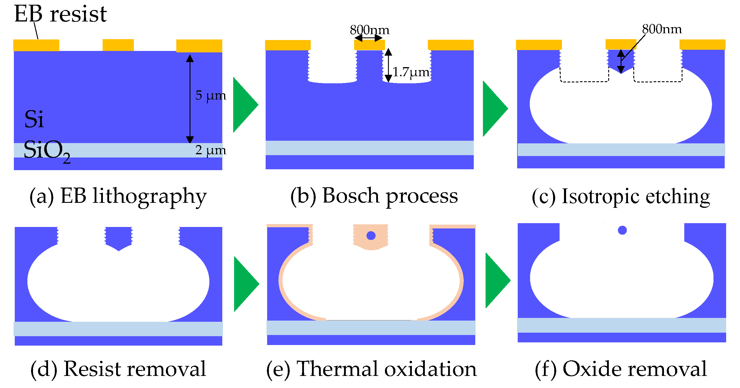
Firstly, the window openings on the 7 mm square oxide-covered chip were created at the areas where the SiNWs were going to be fabricated. The photoresist was used for masking and a buffered hydrofluoric acid solution with surfactant (LAL-1000, Stella Chemifa, Osaka, Japan) was used for the etching. Then, 800 nm wide tensile specimens were patterned using EB lithography (ELS-F125HS, Elionix, Hachioji, Japan). The SiNWs of 800 nm square in the cross section were then fabricated using the two step etching of the Bosch process and isotropic etching (Figure 3).
The SiNWs were thinned using oxidation thinning. We also tried to fabricate 100 nm wide and thick SiNWs using a 100 nm wide mask pattern and dry etching [23]. However, the thickness control was difficult and the side surfaces were rough, which meant that the tensile strength was low. Therefore, we employed a combination of dry etching and oxide thinning in this work. In the oxidation thinning of the silicon nanowire, it was known that the oxidation process was suppressed by stress so as to limit the thinness of the wire [24]. However, in this research, this self-limiting process was not used to obtain a thinner wire. The device chip was oxidized, using a furnace, (MILA-5000, Advance Riko, Yokohama, Japan) at 1100 °C in dry oxygen, in which the self-limiting did not occur [25]. In order to control the diameter of the SiNW, the oxidation process was repeated twice in some conditions. In that case, the oxide layer was removed by a vapor HF etching between the oxidations.
4. Measurement Procedure
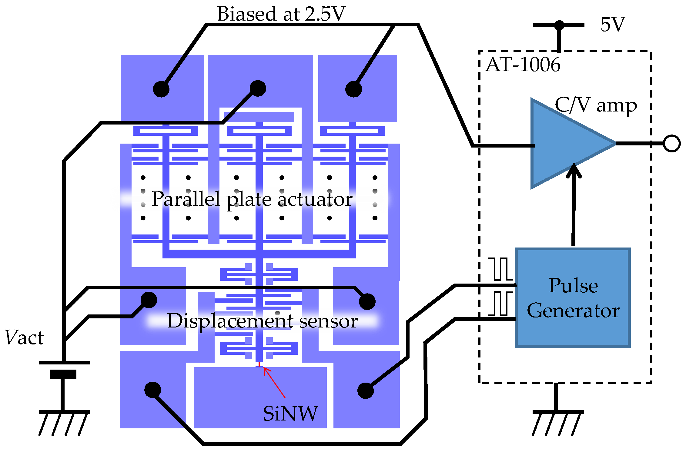
The fabricated chips were mounted on 28-pin dual-in-line packages (DIPs). Wire bonding using aluminum wires was utilized for the electrical connections. The circuit diagram for tensile testing is shown in Figure 4. A multi-axis capacitive accelerometer interface integrated circuit (IC) (AT-1006, ACT-LSI, Atsugi, Japan) was used for capacitance detection at the differential capacitance of the displacement sensor. The sensitivity of the IC was 150 V/pF at its maximum. The actuation voltage was applied with consideration of the bias voltage for the capacitance detection. The moving part was biased at 2.5 V by the capacitance amplifier.
The tensile testing was conducted first. The voltage at the parallel plate actuator was slowly increased from 2.5 V until the output of the displacement sensor was jumped up and saturated. The saturation indicated a pull-in of the capacitances at the displacement sensor, which was caused by the sudden fracture of the specimens. After checking the specimen’s fracture, the obtained voltage–displacement curves were converted to stress–strain curves with the following calibration steps. The calibration was undertaken for each specimen because of the fabrication variation that has been described below.
Firstly, the displacement sensor was calibrated. The device was actuated again to measure the voltage-capacitance relationships. The displacement sensitivity was calculated and the voltage–displacement relationship was calculated with the observed maximum displacement, using a digital microscope. The force that was applied on the specimen was calculated from the finite element analysis that considered the shrinkage of the dimensions, which was caused by the oxidation thinning process. The change in dimensions (width) was measured directly with a scanning electron microscope. Finally, the tapered part at both ends of the specimen was taken into account in the measured displacement. The tensile force–displacement curve was thus obtained. The tensile stress was calculated from the measured width and thickness by assuming that the cross section was ellipsoidal. The tensile strain was calculated by dividing the elongation with the initial length of the test part.
5. Results
5.1. SiNW Device Fabrication
A fabricated tensile testing device with a free standing SiNW is shown in Figure 5. The parallel plate electrostatic comb actuator and capacitive displacement sensor were in 5 μm thick structures, and the SiNW was a few hundred nanometers thick. They were all made in the same device layer of the SOI wafer. Table 1 lists the device design, process conditions for oxidation thinning, and the fabricated width of the four devices that were used for the tensile testing. The width of the SiNWs ranged from 100–200 nm. As a result of the variation in the EB lithography, the width varied significantly and no clear relationship to the oxidation time was observed. Therefore, the dimensions of the specimens were measured using field emission scanning electron microscope (FESEM) observation and all of the specimens are shown in Figure 6. The dimensions of the test device structures were also reduced by oxidation thinning. The width of the beams was measured and the change from the designed width was 330–480 nm, depending on the oxidation time, as listed in Table 1.
5.2. Tensile Testing
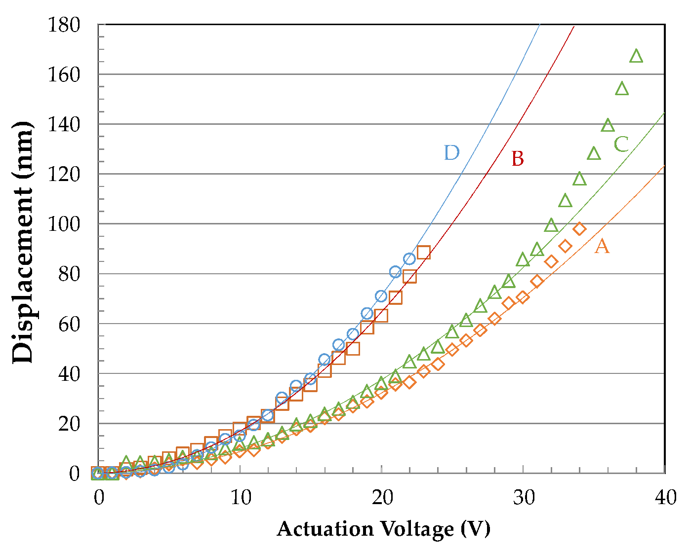
Figure 7 shows the calculated displacement against the voltage on the electrostatic actuator. The specimens were fractured at 22–38 V. The summary of the test results is shown in Table 2. The specimens after testing are shown in Figure 6. The center part of the specimen was missing. The fracture surface of Specimen A is shown in Figure 8.
The calibration test determined the displacement sensitivity as 10.5–13.3 V/μm, depending on the actual dimensions of the testing device. Using the calculated stiffness of the tapered part of the specimen, the force–displacement and stress–strain curves are plotted in Figure 9. The tensile strength ranged from 2.6–4.1 GPa for four samples. All samples showed a brittle fracture and the center part was missing on each of the fractures due to catastrophic fracture at high tensile strengths.
6. Discussion
The dimensions of the testing device were reduced by about 350 nm. One of the reasons for this was the oxidation thinning process. From the Deal–Groove model [26], the oxide thickness had increased by 91 nm and 120 nm when the silicon that was covered with 800 nm oxide was oxidized for 6 h and 8 h, in a dry oxidation process at 1100 °C, which consumed 42 nm and 56 nm of silicon, respectively. The consumption of silicon during the second oxidation was not known, since the remaining oxide thickness after stripping the oxide on the SiNWs was not controlled or measured. Assuming that the remaining oxide thickness was 400 nm, considering the over-etching time in the stripping, the consumption of the silicon layer was only a few nanometers. The rest of the difference would have been caused by the lithography process.
The smaller width of the structure caused a larger gap between the parallel plates, which reduced the electrostatic force and capacitance change. The electrostatic force reduced by 25% from the designed value, which made the actuation voltage higher on testing. The displacement sensitivity was about 12 V/μm, which was smaller by 35%, because the initial gap was wider. The measured noise level of the voltage output of the circuit was 10.3 mVrms, which corresponded to a displacement of 0.9 nm. This was about 1% of the total displacement and it was sufficient for the experiments.
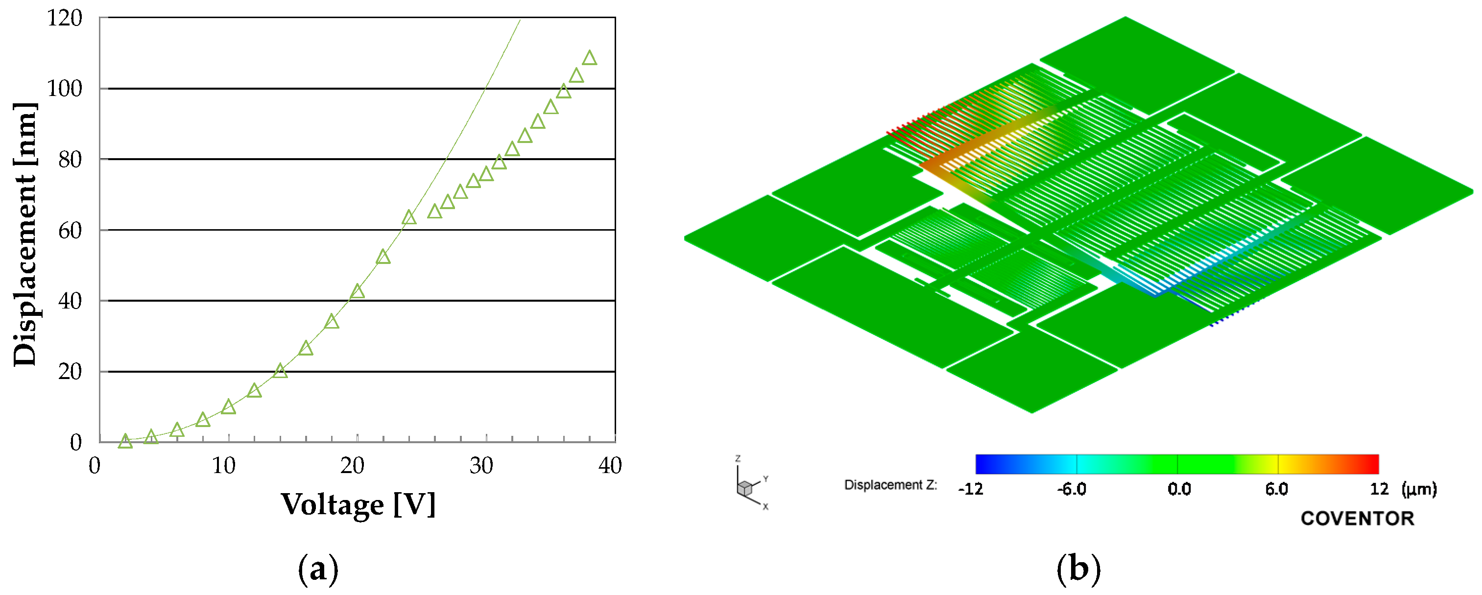
The force–displacement curves of the test results showed good linearity up to an 80 nm displacement. Then, nonlinearity was observed at larger displacements, which was likely as a result of the nonlinearity of the electrostatic transducer. The electrostatic force of the parallel plate actuator was proportional to the square of the voltage and inversely proportional to the square of the gap. We have took into account this effect in the design, but we did not consider the effect of lateral bending of the thin and long electrodes. The whole device structure was further analyzed using the finite element analysis (CoventorWare, Coventor, Cary, NC, USA). There was bending of the electrode beams, however, the capacitance change against the displacement showed a small nonlinearity, which did not explain the voltage–displacement observed nonlinearity in the force–displacement relationship. On the other hand, the voltage–displacement curve in Figure 10a indicates that the displacement did not follow the square of the voltage at a displacement of more than 80 nm. At this displacement range, we found that the device started to tilt around the tensile axis (Figure 10b) and that the force was reduced as a result of the reduction of the overlapped area of the parallel plate electrostatic actuators. Insufficient support at both sides of the device caused the tilt. Therefore, the force might have been overestimated at the large displacement region. However, it was difficult to calculate the amount of the overestimation in our measurement results, as the actual tilting angle might have been different from the simulated results, because the rotation was unstable and might have changed.
Large deviations were seen in the slopes of the stress–strain curves, the main reason for which was the thick non-uniformity of the SiNWs. As we can see in some of the specimens in Figure 6 and in the enlarged view of specimen A in Figure 11, the bottom of the SiNW had a large degree of waviness and the calculated Young’s modulus showed a large deviation. The thickness of the specimens was measured at the fracture surface and was the smallest in this specimen, which caused the overestimation of stiffness. From the SEM image in Figure 6, the thickness variations ranged from 10 to 100%. For example, specimen A showed a uniform thickness and the measured Young’s modulus agreed well with the theoretical value. On the other hand, specimen D showed a large variation in thickness, which resulted in the larger value of the Young’s modulus. The reason for the waviness was the uneven width of the EB resist pattern and the non-uniform opening width for the SiNW etching process. Both of which had caused the thickness variation of the sidewall passivation layer during the DRIE process, which resulted in a low controllability of the thickness dimensions. As mentioned above, the thickness uniformity of the EB resist should have been improved by optimizing the coating process, and the width of the openings near the specimen should have been revised.
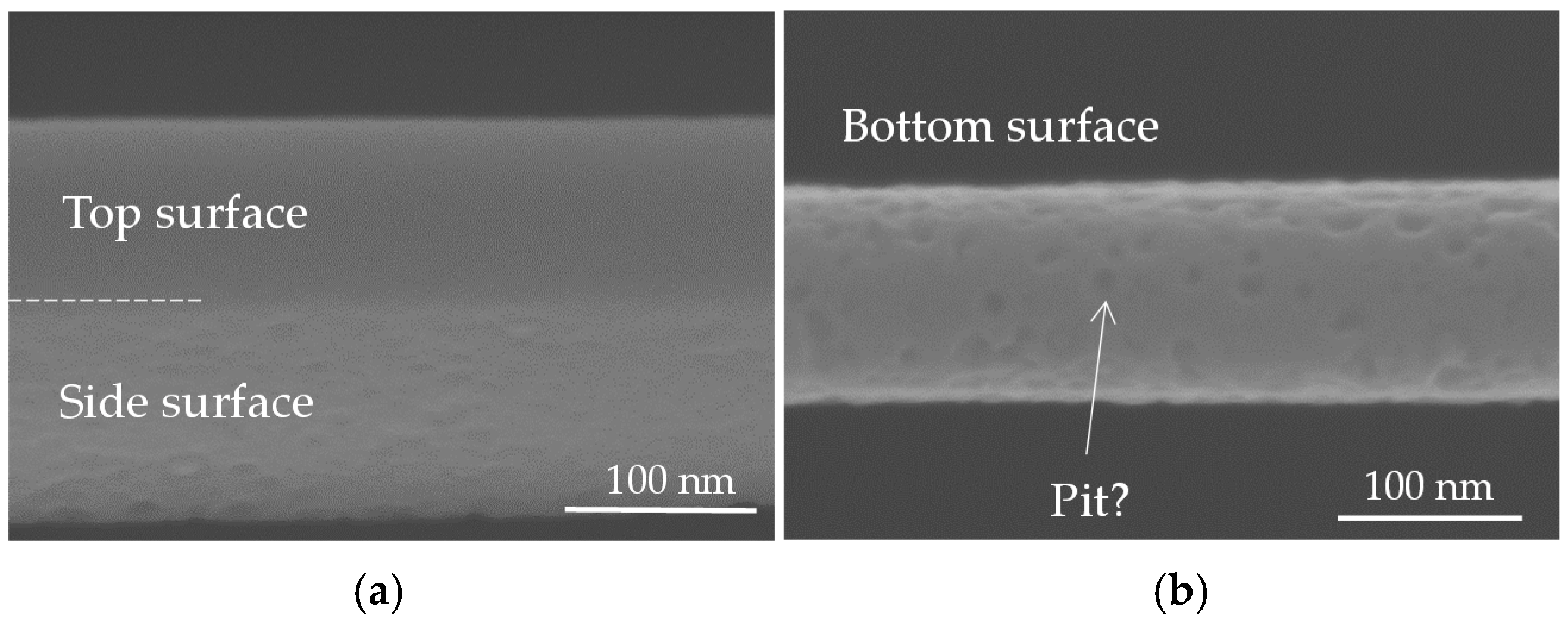
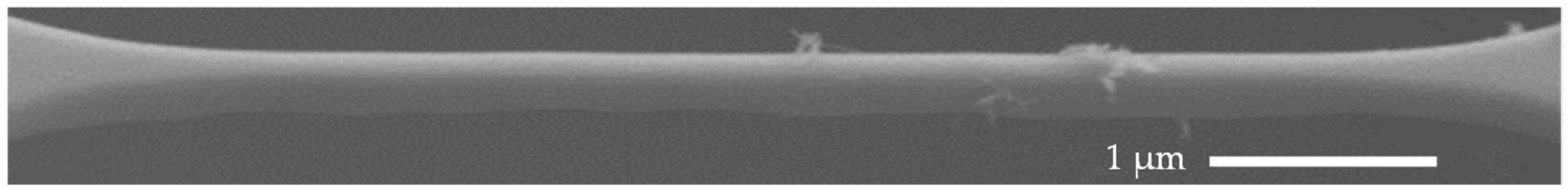
The tensile strength was comparable to the microscale specimens [27], which we did not expect to find. As a result of the surface oxidation process, the surface of the silicon would have been smoothed of any roughness that was caused by patterning, such as the jagged edge of the EB resist and the scallops that were generated in the Bosch process. The top surface was smooth (as seen in Figure 6), whereas the side and bottom surfaces had a degree of roughness (as seen in Figure 12). The size of the pit in these surfaces was about 10 nm, and it might have acted as the fracture origin [28]. The roughness of the SF6 etching on the side and bottom surfaces was not removed by oxidation or oxide precipitation during the oxidation thinning process. We needed to improve the process in order to obtain a higher strength and better structural reliability for future applications.
Through the fabrication and operation of the electrostatic MEMS tensile testing device with integrated SiNW, we confirmed that the proposed fabrication process integrated a SiNW into the micrometer scale Si MEMS structures, using a top down fabrication process. This process would be useful for further miniaturization of sensors and actuators, such as those that are required for piezoresistive sensors and torsional mirror devices.
7. Conclusions
The tensile testing of SiNWs batch-integrated into micrometer scale Si MEMS structures was conducted using an electrostatic tensile testing device. SiNWs of about 100 nm in diameter and 5 μm in length were successfully fabricated into the 5 μm thick device layer of an SOI wafer, using a combination of the Bosch process and isotropic undercut etching. In addition, a sacrificial oxidation thinning process was used to control the diameter and remove the damage during the plasma etching processes. The tensile strength was successfully measured as 2.6–4.1 GPa, which was comparable to that of the microscale specimens and was adequate for the device applications, however, it needed to be improved by reducing the roughness that was caused by the oxidation process and the non-uniformity of the thickness.
Supplementary Materials
The details of the device design are available online at https://www.mdpi.com/2076-3417/8/6/880/s1. Figure S1: Schematic of tensile testing device; Figure S2: Unit design of parallel plate electrostatic actuator; Figure S3: Calculation of parallel drive actuator; Figure S4: Unit design capacitive displacement sensor; Figure S5: Differential capacitance change of displacement sensor; Figure S6: Electrostatic differential force generated by displacement senor; Figure S7: Type A spring; Figure S8: Type B spring; Table S1: Design target values and specifications; Table S2: Design value of parallel drive actuator; Table S3: Design value of displacement sensor; Table S4: Parameters of designed spring (Type A); Table S5: Parameters of designed spring (Type B); Table S6: Spring constants.
Author Contributions
T.T. and O.T. conceived and designed the experiments; J.S. and T.H. designed and fabricated the devices; T.H. and T.T. analyzed the data; T.T. wrote the paper; and all of the authors discussed the results and contributed to the writing and editing of the manuscript.
Acknowledgments
This work was supported by JSPS KAKENHI Grant Number 26600062. A part of this work was supported by Kyoto University Nano Technology Hub in ‘Nanotechnology Platform Project’, which was sponsored by the Ministry of Education, Culture, Sports, Science, and Technology (MEXT), Japan. The authors would like to thank to K. Ishikawa and T. Sumigawa for their help on the SEM observation.
Conflicts of Interest
The authors declare no conflict of interest.
References
- Smith, A.D.; Niklaus, F.; Paussa, A.; Vaziri, S.; Fischer, A.C.; Sterner, M.; Forsberg, F.; Delin, A.; Esseni, D.; Palestri, P.; et al. Electromechanical piezoresistive sensing in suspended graphene membranes. Nano Lett. 2013, 13, 3237–3242. [Google Scholar] [CrossRef] [PubMed]
- Sayed, S.; Gamil, M.; El-Bab, A.F.; Nakamura, K.; Tsuchiya, T.; Tabata, O.; El-Moneim, A.A. Graphene film development on flexible substrate using a new technique: Temperature dependency of gauge factor for graphene-based strain sensors. Sens. Rev. 2016, 36, 140–147. [Google Scholar] [CrossRef]
- Lee, S.-W.; Muoth, M.; Hierold, C. Photomask-based integration process of low-defect suspended carbon nanotubes into SOI MEMS. Nanotechnology 2014, 25, 215301. [Google Scholar] [CrossRef] [PubMed]
- Shiomi, Y.; Hirai, Y.; Tabata, O.; Tsuchiya, T. High-yield bridged assembly of ssDNA-modified SWCNT using dielectrophoresis. Int. J. Autom. Technol. 2018, 12, 29–36. [Google Scholar] [CrossRef]
- Tsuchiya, T.; Ura, Y.; Sugano, K.; Tabata, O. Electrostatic tensile testing device with nanonewton and nanometer resolution and its application to C60 nanowire testing. J. Microelectromech. Syst. 2012, 21, 523–529. [Google Scholar] [CrossRef]
- Bai, J.; Ma, T.; Chu, W.; Wang, R.; Silva, L.; Michal, C.; Chiao, J.C.; Chiao, M. Regenerated spider silk as a new biomaterial for MEMS. Biomed. Microdevices 2006, 8, 317–323. [Google Scholar] [CrossRef] [PubMed]
- Funakoshi, K.; Suzuki, H.; Takeuchi, S. Lipid bilayer formation by contacting monolayers in a microfluidic device for membrane protein analysis. Anal. Chem. 2006, 78, 8169–8174. [Google Scholar] [CrossRef] [PubMed]
- Malmstadt, N.; Nash, M.A.; Purnell, R.F.; Schmidt, J.J. Automated formation of lipid-bilayer membranes in a microfluidic device. Nano Lett. 2006, 6, 1961–1965. [Google Scholar] [CrossRef] [PubMed]
- Yamahata, C.; Collard, D.; Legrand, B.; Takekawa, T.; Kumemura, M.; Hashiguchi, G.; Fujita, H. Silicon nanotweezers with subnanometer resolution for the micromanipulation of biomolecules. J. Microelectromech. Syst. 2008, 17, 623–631. [Google Scholar] [CrossRef]
- Akishiba, T.; Tamura, N.; Ichii, T.; Hirai, Y.; Sugano, K.; Tsuchiya, T.; Sugimura, H.; Tabata, O. DNA origami assembly on patterned silicon by AFM based lithography. In Proceedings of the 26th IEEE International Conference on Micro Electro Mechanical Systems (MEMS 2013), Taipei, Taiwan, 20–24 January 2013; pp. 307–310. [Google Scholar]
- Takeshita, T.; Suekuni, K.; Aiba, K.; Sugano, K.; Isono, Y. Surface-Enhanced Raman Spectroscopy Analysis Device with Gold Nanoparticle Arranged Nanochannel. Electron. Commun. Jpn. 2017, 100, 33–41. [Google Scholar] [CrossRef]
- Schwalb, C.H.; Grimm, C.; Baranowski, M.; Sachser, R.; Porrati, F.; Reith, H.; Das, P.; Müller, J.; Völklein, F.; Kaya, A.; et al. A tunable strain sensor using nanogranular metals. Sensors 2010, 10, 9847–9856. [Google Scholar] [CrossRef] [PubMed]
- Peng, K.; Xu, Y.; Wu, Y.; Yan, Y.; Lee, S.-T.; Zhu, J. Aligned single-crystalline Si nanowire arrays for photovoltaic applications. Small 2005, 1, 1062–1067. [Google Scholar] [CrossRef] [PubMed]
- Li, Z.; Chen, Y.; Li, X.; Kamins, T.I.; Nauka, K.; Williams, R.S. Sequence-Specific Label-Free DNA Sensors Based on Silicon Nanowires. Nano Lett. 2004, 4, 245–247. [Google Scholar] [CrossRef]
- Feng, X.L.; He, R.; Yang, P.; Roukes, M.L. Very high frequency silicon nanowire electromechanical resonators. Nano Lett. 2007, 7, 1953–1959. [Google Scholar] [CrossRef]
- Cui, Y.; Wei, Q.; Park, H.; Lieber, C.M. Nanowire nanosensors for highly sensitive and selective detection of biological and chemical species. Science 2001, 293, 1289–1292. [Google Scholar] [CrossRef] [PubMed]
- Toriyama, T.; Tanimoto, Y.; Sugiyama, S. Single crystal silicon nano-wire piezoresistors for mechanical sensors. J. Microelectromech. Syst. 2002, 11, 605–611. [Google Scholar] [CrossRef]
- He, R.; Feng, X.L.; Roukes, M.L.; Yang, P. Self-transducing silicon nanowire electromechanical systems at room temperature. Nano Lett. 2008, 8, 1756–1761. [Google Scholar] [CrossRef] [PubMed]
- Robert, P.; Nguyen, V.; Hentz, S.; Duraffourg, L.; Jourdan, G.; Arcamone, J.; Harrisson, S. M&NEMS: A new approach for ultra-low cost 3D inertial sensor. In Proceedings of the IEEE Sensors (SENSORS 2009), Christchurch, New Zealand, 25–28 October 2009; pp. 963–966. [Google Scholar] [CrossRef]
- Fujii, T.; Sudoh, K.; Inoue, S.; Namazu, T. Design and development of electrostatically driven uniaxial tensile test device for silicon nanowires. Sens. Mater. 2016, 28, 89–102. [Google Scholar] [CrossRef]
- Zhang, D.; Breguet, J.M.; Clavel, R.; Sivakov, V.; Christiansen, S.; Johann Michler, J. In situ electron microscopy mechanical testing of silicon nanowires using electrostatically actuated tensile stages. J. Microelectromech. Syst. 2010, 19, 663–673. [Google Scholar] [CrossRef]
- Zhu, Y.; Xu, F.; Qin, Q.; Fung, W.Y.; Lu, W. Mechanical properties of Vapor−Liquid−Solid synthesized silico nanowires. Nano Lett. 2009, 9, 3934–3939. [Google Scholar] [CrossRef] [PubMed]
- Tsuchiya, T.; Hemmi, T.; Suzuki, J.; Hirai, Y.; Tabata, O. Tensile fracture of integrated single-crystal silicon nanowire using MEMS electrostatic testing device. Procedia Struct. Integr. 2016, 2, 1405–1412. [Google Scholar] [CrossRef]
- Kedzierski, J.; Bokor, J. Fabrication of planar silicon nanowires on silicon-on-insulator using stress limited oxidation. J. Vac. Sci. Technol. B 1997, 15, 2825–2828. [Google Scholar] [CrossRef]
- Liu, H.I.; Biegelsen, D.K.; Ponce, F.A.; Johnson, N.M.; Pease, R.F.W. Self limiting oxidation for fabricating sub 5 nm silicon nanowires. Appl. Phys. Lett. 1994, 64, 1383–1385. [Google Scholar] [CrossRef]
- Deal, B.E.; Grove, A.S. General Relationship for the Thermal Oxidation of Silicon. J. Appl. Phys. 1965, 36, 3770–3778. [Google Scholar] [CrossRef]
- Uesugi, A.; Hirai, Y.; Sugano, K.; Tsuchiya, T.; Tabata, O. Effect of crystallographic orientation on tensile fractures of (100) and (110) silicon microstructures fabricated from SOI wafers. Micro Nano Lett. 2015, 10, 678–682. [Google Scholar] [CrossRef] [Green Version]
- Tsuchiya, T.; Miyamoto, K.; Sugano, K.; Tabata, O. Fracture behavior of single crystal silicon with thermal oxide layer. Eng. Fract. Mech. 2016, 163, 523–532. [Google Scholar] [CrossRef]
Figure 1.
Design of electrostatic tensile testing device. (a) Schematic diagram. Light blue parts indicate the fixed regions; (b) mask design.
Figure 1.
Design of electrostatic tensile testing device. (a) Schematic diagram. Light blue parts indicate the fixed regions; (b) mask design.
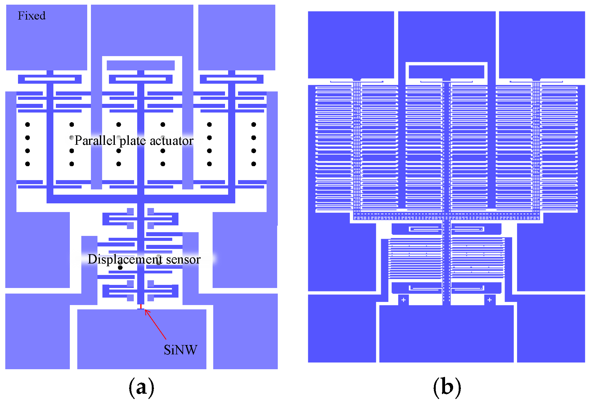
Figure 2.
Fabrication process flow. EB—electron beam; SiNW—silicon nanowire; PECVD—plasma enhanced chemical vapor deposition; DRIE—deep reactive ion etching.
Figure 2.
Fabrication process flow. EB—electron beam; SiNW—silicon nanowire; PECVD—plasma enhanced chemical vapor deposition; DRIE—deep reactive ion etching.

Figure 3.
SiNW fabrication process. For further thinning, steps (e,f) are repeated twice.

Figure 4.
Tensile test circuit setup. The common input of interface integrated circuit (IC) is biased at 2.5 V, which is half of the power supply. The actuation voltage has an offset of 2.5 V.
Figure 4.
Tensile test circuit setup. The common input of interface integrated circuit (IC) is biased at 2.5 V, which is half of the power supply. The actuation voltage has an offset of 2.5 V.

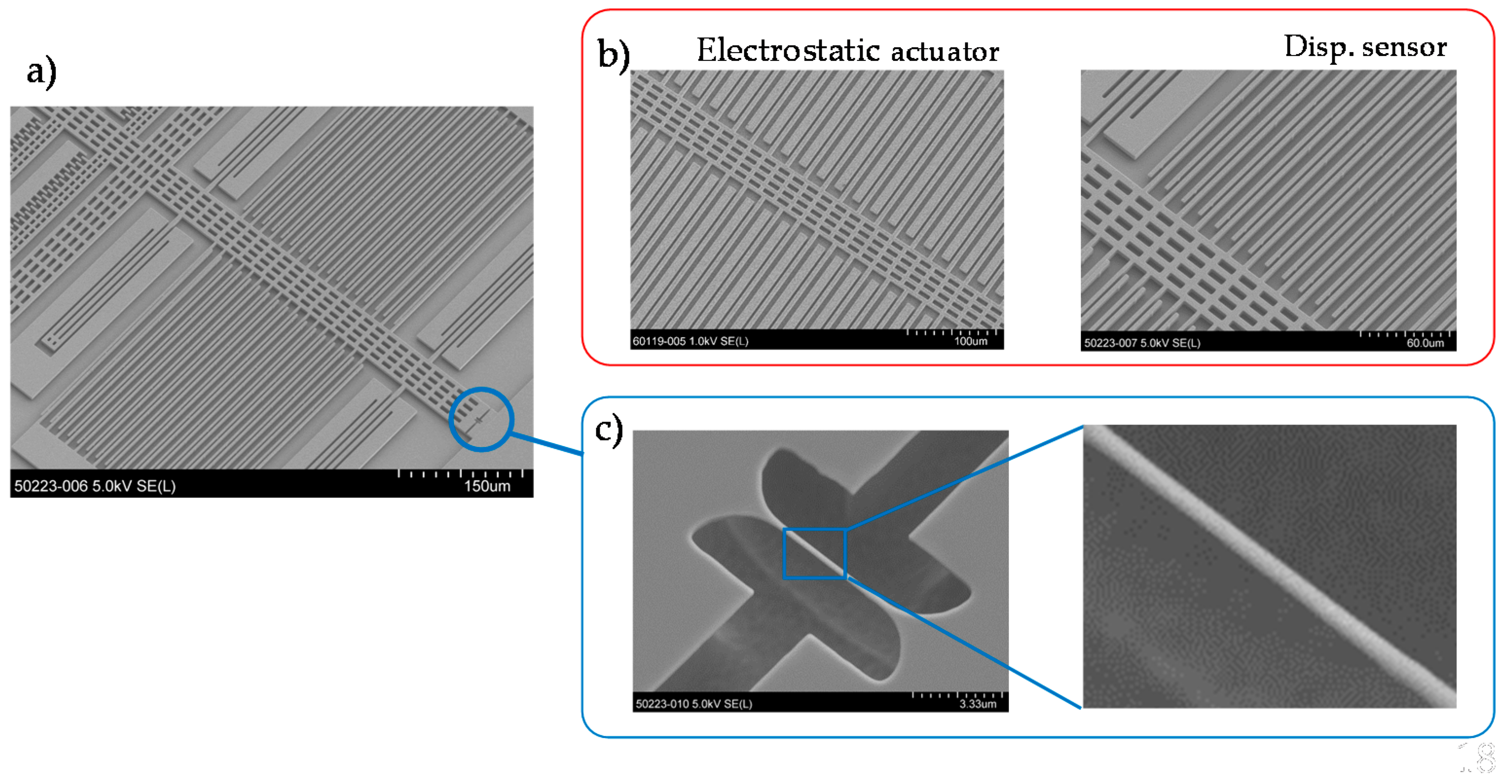
Figure 5.
Fabricated device. (a) Center moving part with the displacement sensor supported by the suspending beams. The electrostatic actuator is located upper left of this image. (b) Close-up view of the electrostatic actuator and the displacement sensor. (c) Close-up view of the SiNW specimen.
Figure 5.
Fabricated device. (a) Center moving part with the displacement sensor supported by the suspending beams. The electrostatic actuator is located upper left of this image. (b) Close-up view of the electrostatic actuator and the displacement sensor. (c) Close-up view of the SiNW specimen.

Figure 6.
Tensile-tested specimens. (Upper row) before testing. (Lower row) after fracture.
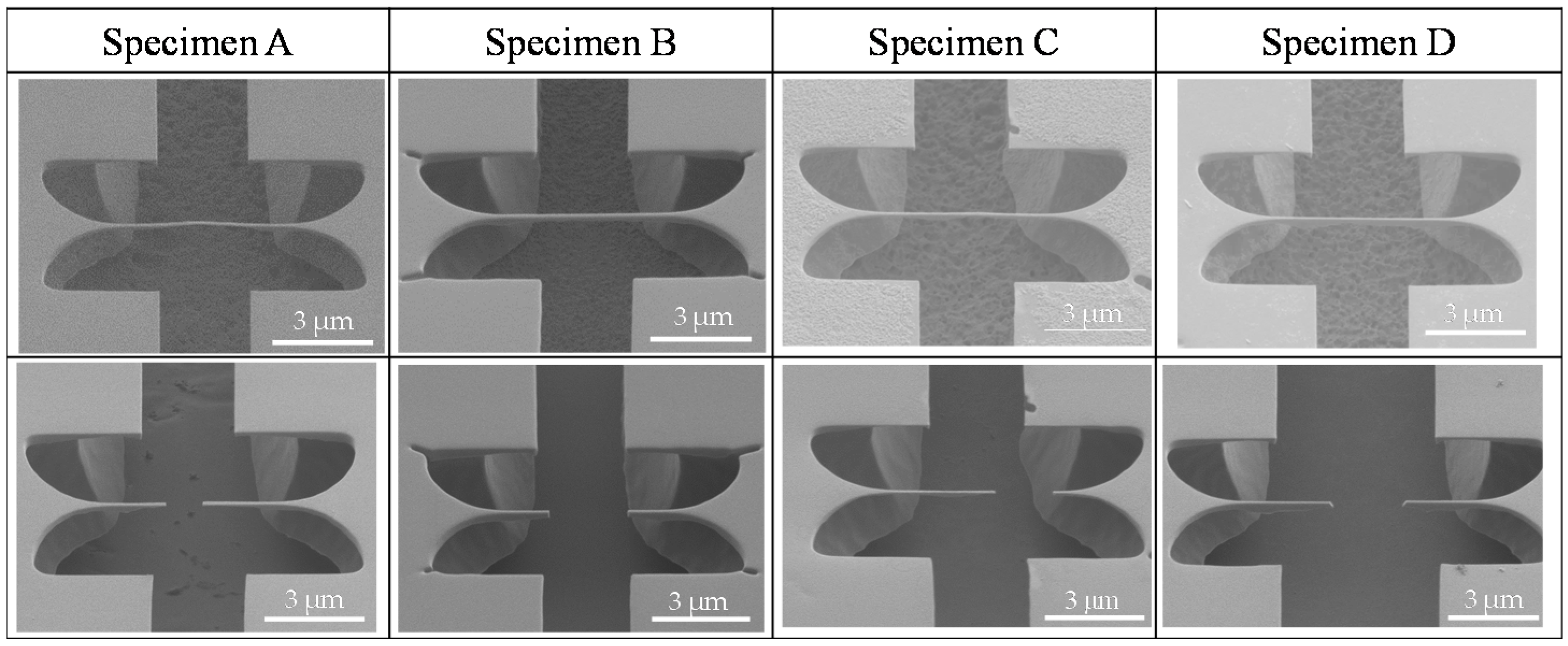
Figure 7.
Measured displacement of all of the specimens A–D against applied actuation voltage on the electrostatic actuator. Specimens were fractured at the highest voltage of the plots. Fitting lines indicate quadratic function.
Figure 7.
Measured displacement of all of the specimens A–D against applied actuation voltage on the electrostatic actuator. Specimens were fractured at the highest voltage of the plots. Fitting lines indicate quadratic function.

Figure 8.
Fracture surface of Specimen A.
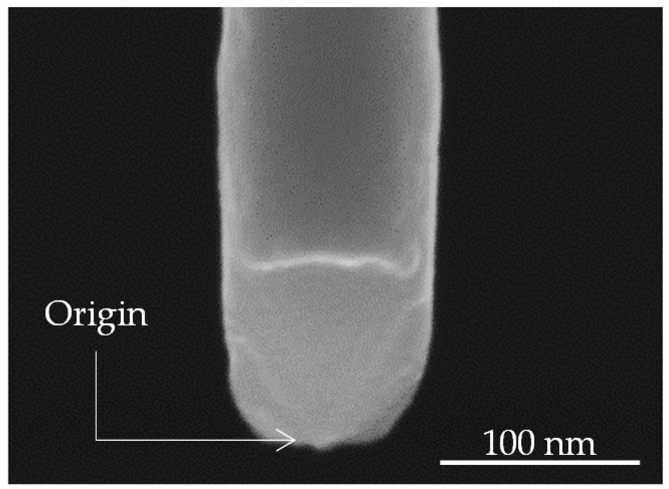
Figure 9.
(a) Force–displacement plots and (b) tensile stress–strain plots. Lines indicates linear fittings. Note that fitting is done on a linear range (up to 80 nm displacement) for Specimen C.
Figure 9.
(a) Force–displacement plots and (b) tensile stress–strain plots. Lines indicates linear fittings. Note that fitting is done on a linear range (up to 80 nm displacement) for Specimen C.
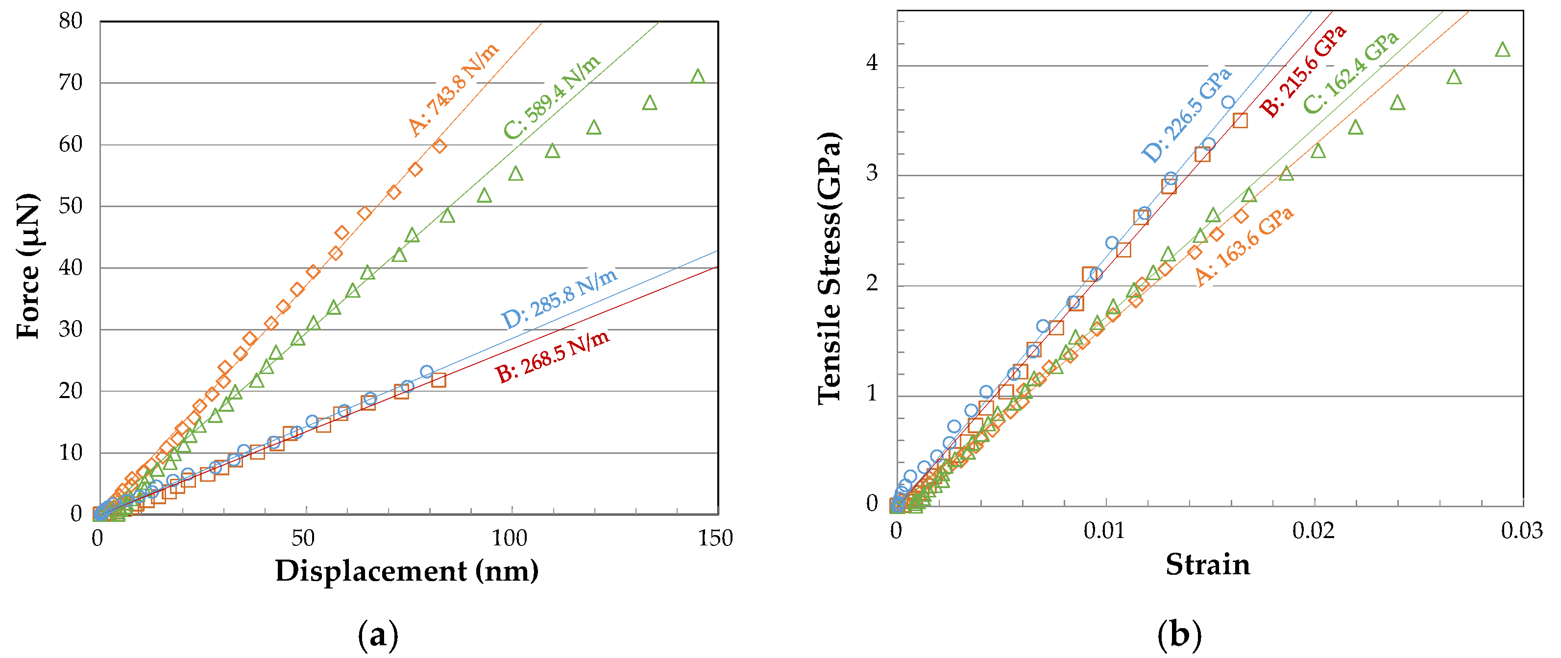
Figure 10.
(a) Simulated displacement of the device with specimen C against the applied voltage. The line plot is a fitting curve to the quadrature function. (b) Simulated deformation at 38 V. Displacement is exaggerated by five times. The contour plot indicates z-axis (vertical) displacement.
Figure 10.
(a) Simulated displacement of the device with specimen C against the applied voltage. The line plot is a fitting curve to the quadrature function. (b) Simulated deformation at 38 V. Displacement is exaggerated by five times. The contour plot indicates z-axis (vertical) displacement.

Figure 11.
Enlarged view of specimen A before tensile testing.

Figure 12.
(a) Oblique and (b) bottom side views of a part of a specimen after tensile testing.

Table 1.
Properties of tested specimens. Details on two types of device design are described in the Supplemental Material. Specimen width and linewidth reduction in test device structures were measured after oxidation.
Table 1.
Properties of tested specimens. Details on two types of device design are described in the Supplemental Material. Specimen width and linewidth reduction in test device structures were measured after oxidation.
| Specimen | A | B | C | D |
|---|---|---|---|---|
| Device design | type 1 | type 2 | type 2 | type 1 |
| First oxidation time (min) | 480 | 360 | 360 | 360 |
| Second oxidation time (min) | - | 40 | 30 | 40 |
| Specimen width (nm) | 188 | 128 | 103 | 142 |
| Linewidth reduction (nm) | 387 | 330 | 353 | 361 |
Table 2.
Summary of the tensile testing results.
| Specimen | A | B | C | D |
|---|---|---|---|---|
| Displacement sensitivity (V/μm) | 11.4 | 10.5 | 11.7 | 13.3 |
| Voltage fractured (V) | 35 | 23 | 38 | 22 |
| Estimated stiffness of tapered part (N/m) | 9452 | 4870 | 6375 | 6959 |
| Stiffness of specimen (N/m) | 742.4 | 268.5 | 590.5 | 285.8 |
| Measured width (nm) | 190 | 130 | 106 | 134 |
| Measured thickness (nm) | 152 | 61 | 206 | 60 |
| Young’s modulus (GPa) | 163.6 | 215.6 | 162.4 | 226.5 |
| Tensile strength (GPa) | 2.6 | 3.5 | 4.1 | 3.7 |
© 2018 by the authors. Licensee MDPI, Basel, Switzerland. This article is an open access article distributed under the terms and conditions of the Creative Commons Attribution (CC BY) license (http://creativecommons.org/licenses/by/4.0/).
Share and Cite
MDPI and ACS Style
Tsuchiya, T.; Hemmi, T.; Suzuki, J.-y.; Hirai, Y.; Tabata, O. Tensile Strength of Silicon Nanowires Batch-Fabricated into Electrostatic MEMS Testing Device. Appl. Sci. 2018, 8, 880. https://doi.org/10.3390/app8060880
AMA Style
Tsuchiya T, Hemmi T, Suzuki J-y, Hirai Y, Tabata O. Tensile Strength of Silicon Nanowires Batch-Fabricated into Electrostatic MEMS Testing Device. Applied Sciences. 2018; 8(6):880. https://doi.org/10.3390/app8060880
Chicago/Turabian StyleTsuchiya, Toshiyuki, Tetsuya Hemmi, Jun-ya Suzuki, Yoshikazu Hirai, and Osamu Tabata. 2018. "Tensile Strength of Silicon Nanowires Batch-Fabricated into Electrostatic MEMS Testing Device" Applied Sciences 8, no. 6: 880. https://doi.org/10.3390/app8060880
Note that from the first issue of 2016, this journal uses article numbers instead of page numbers. See further details here.