Strained Silicon Single Nanowire Gate-All-Around TFETs with Optimized Tunneling Junctions
by
 ,
,
Keyvan Narimani
1,* ,
,
Stefan Trellenkamp
2,
Andreas Tiedemann
1,
Siegfried Mantl
1 and
Qing-Tai Zhao
1,* 
1
Peter-Grünberg-Institute (PGI 9), JARA-Fundamentals for Future Technology, Forschungszentrum Jülich, 52428 Jülich, Germany
2
HNF, Forschungszentrum Jülich, 52428 Jülich, Germany
*
Authors to whom correspondence should be addressed.
Appl. Sci. 2018, 8(5), 670; https://doi.org/10.3390/app8050670
Submission received: 15 March 2018
/
Revised: 11 April 2018
/
Accepted: 20 April 2018
/
Published: 26 April 2018
(This article belongs to the Special Issue Silicon Nanowires and Their Applications)
Abstract
:In this work, we demonstrate a strained Si single nanowire tunnel field effect transistor (TFET) with gate-all-around (GAA) structure yielding Ion-current of 15 μA/μm at the supply voltage of Vdd = 0.5V with linear onset at low drain voltages. The subthreshold swing (SS) at room temperature shows an average of 76 mV/dec over 4 orders of drain current Id from 5 × 10⁻⁶ to 5 × 10⁻² µA/µm. Optimized devices also show excellent current saturation, an important feature for analog performance.
1. Introduction
Scaling of complementary metal oxide semiconductor (CMOS) technology has brought about significant improvements in terms of power dissipation, device density, switching frequency, and costs reductions. Continued reduction of device dimensions into the nanometers range faces major issues with the high leakage current, unscalability of supply voltage Vdd, and lowered Ion/Ioff switching ratio. The main constraint of metal-oxide-semiconductor field-effect transistor (MOSFET) for addressing these issues is the inverse subthreshold swing SS (=), which is limited to 60 mV/dec at room temperature. Therefore, any attempt to scale Vdd by adjusting threshold voltage Vth will lead to exponentially higher Ioff-current, deteriorating the switching ratio. To enable further Vdd scaling, steep slope device concepts (SS < 60 mV/dec) are required. The tunnel field effect transistor (TFET) is a promising alternative following the experimental demonstration of its sub-60 mV/dec swing [1]. TFET relies on quantum band-to-band tunneling (BTBT) to inject carriers from the source to the channel while cutting off the high-energy tail of the Fermi distribution, essentially having a similar effect to cooling down the distribution. Various research studies have demonstrated TFETs with SS < 60 mV/dec based on different materials like Si [2], Ge [3], SiGe [4], and III-V [5]. In comparison to the other materials, silicon-based TFETs generally show better performance in terms of minimum SS and switching ratio, mainly due to the maturity of silicon fabrication technology. Moreover, silicon TFETs are compatible with the conventional CMOS fabrication process, which keeps the costs low and makes it feasible to realize complementary TFET circuits [6,7].
By employing innovative materials, like high-k oxide and thin strained silicon, and highly scaled device structures, like nanowires (NWs), silicon TFETs have achieved promising results for both n- and p-type devices [8]. It is worth noting that these devices were based on an array of nanowires. The final results reflect the average behavior of all the NWs, dismissing the variations of each individual NW in the array. This stems from the fact that the tunneling probability at the source of TFETs has exponential dependence on process-related parameters, such as nanowire shape and doping profile. By means of simulation, C.-J. Chen et al [9] have shown that TFETs are more susceptible to process variations than MOSFETs. Consequently, a single NW is superior for optimization of TFETs. In this work, we seek to fabricate gate-all-around (GAA) TFETs based on a single NW with a top-down approach to optimize the key fabrication processes, namely ion implantation and dopant activation, thus enabling us to draw specific conclusions at each step to further improve the Ion-current and average SS.
2. Device Fabrication
Single nanowire GAA TFETs were fabricated on strained silicon-on-insulator (sSOI) wafers with 15 nm biaxially strained silicon (biax,tensile = 0.8%) and 145 nm buried oxide (BOX). Strained silicon, due to its lower effective mass m* and lower bandgap Eg, can achieve better tunneling current [10]. Figure 1 shows the process steps as well as schematics of the final device structure. The single NW was fabricated by a top-down process including e-beam lithography, subsequent reactive ion etching (RIE), and HF dip to suspend the nanowire. The final NW cross-section dimensions are 35 nm × 10 nm. After cleaning the substrate using RCA procedure, 3 nm HfO2 by atomic layer deposition (ALD) and 60 nm TiN using atomic vapor deposition (AVD) were deposited as the high-k/metal gate stack. Then it was patterned using e-beam lithography and etched back by dry and wet etching. A very thin layer of 1.7 nm Ni was deposited by physical vapor deposition (PVD) to form a high quality NiSi2 layer at the source and drain by annealing the substrate at 550 °C in forming gas for 30 s. The unreacted Ni residuals were selectively removed in a mixture of H2O:H2SO4. Ni silicide formed by this method yields good gate alignment without encroachment of silicide in the channel region [11]. Implantation was carried out into the silicide using boron and phosphorous ions with various energies and tilt angles. For each step of the ion implantation, the other side of the device was protected by polymethyl methacrylate (PMMA) photoresist in order to form p+ and n+ junctions. After implantations, the dopants were activated at various temperatures in N2 environment, as will be discussed in the next section. Finally, the substrate was passivated by SiO2 and final Al contacts were formed. Figure 2 shows a side view scanning electron microscope (SEM) image of the finished structure, where the gate completely wraps around the nanowire, leading to improved electrostatic control.
3. Device Characteristics
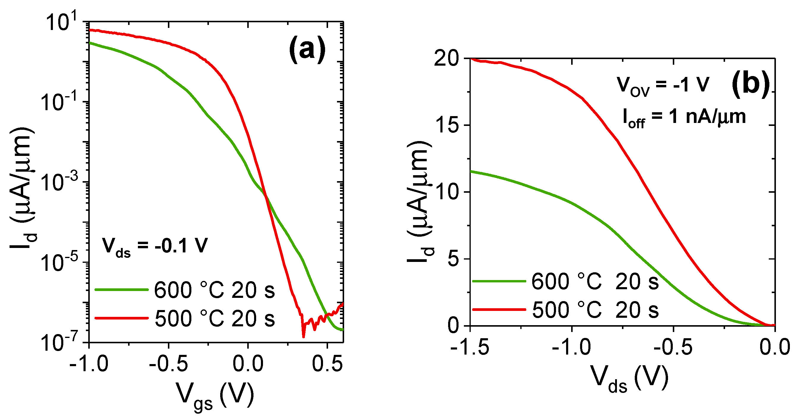
In this part, we will evaluate the effect of implantation and fabrication parameters on the optimized performance of TFETs for high Ion current and minimum average SS. The first set of devices (Set 1) were implanted with P+ ions to a dose of 1 × 1015 cm−2 at an energy of 3 keV and B+ ions to a dose of 5 × 1014 cm−2 at 1.5 keV both at 45° tilt. The reason for a lower B+ dose is to suppress the n-branch of the ambipolar behavior. Samples were activated at two different temperatures of 500 °C and 600 °C for 20 s. Figure 3a depicts the measured transfer characteristics Id-Vgs of the device for a p-TFET. As evident from the figure, the TFET activated at the higher temperature shows degraded SS and lower Ion current compared to the device activated at 500 °C. This is due to the fact that the higher temperature annealing causes more extended diffusion of dopants, hence decreasing the steepness of the tunneling junction. Figure 3b shows the output Id-Vds characteristics for devices at Vov = −1 V, which is defined as Vov = Vgs − Voff = −1 V for an Ioff = 1 nA/um. The typical super-linear onset of drain current Id at small Vds is present in the Id-Vds curves. The super-linear onset stems from drain-induced barrier thinning (DIBT) [12], which can be mitigated by increasing the dopant concentration at the tunneling junction [13]. In other words, for both temperature cases the dopant concentration at the source is lower than the optimum value and needs to be further increased.
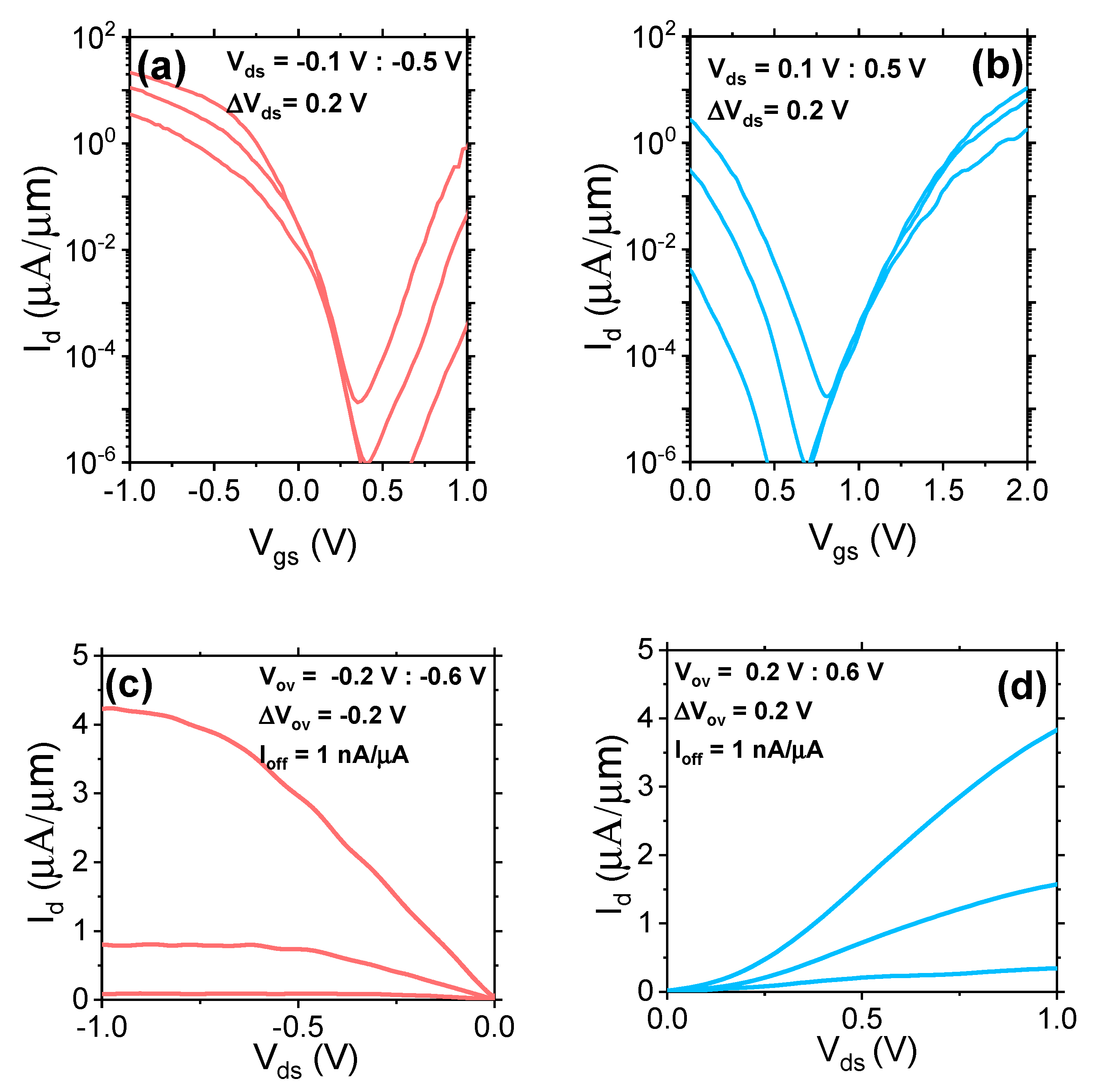
To optimize the device performance, another set of TFETs (Set 2) were fabricated with different implantation and activation parameters. P ions with a dose 5 × 1015 cm−2 and at an energy of 3 keV and B ions with a dose of 1 × 1015 cm−2 at 1.5 keV were implanted at a tilt of +/− 45°, respectively. The implantation doses were increased to provide enough dopant concentration at the junctions after activation. The annealing was carried out at 550 °C for 10 s to drive out the dopants to the silicide/channel interface for dopant segregation. The annealing time and temperature were decreased in order to achieve sharper junctions. Figure 4a,b shows the measured transfer characteristics Id-Vgs for the Set 2 devices of both p- and n-TFETs, respectively. A TFET works in both modes, p- and n-type, due to the presence of tunneling junctions at both the source and drain side, which causes undesired ambipolar switching, a typical behavior of a TFET. Moreover, the p-TFET shows higher on current Ion than n-TFET, corresponding to an Ion of 2.41 µA/µm for p-TFET and 0.78 µA/µm for n-TFET respectively, at Vds = Von = Vg − Voff = −0.5 V for an Ioff = 1 nA/µm. The reason that n-TFETs show lower current could be due to the broader tunneling junction caused by faster B diffusion. For further analysis, Figure 4c,d shows the corresponding output characteristics Id-Vds for p- and n-TFET. The p-TFET shows very good current saturation and more importantly a linear onset. On the other hand, the n-TFET still shows a super-linear onset. Due to the higher diffusion coefficient of boron in silicon in comparison to phosphorus, annealing at 550 °C for 10 s is still not optimal for n-TFETs.
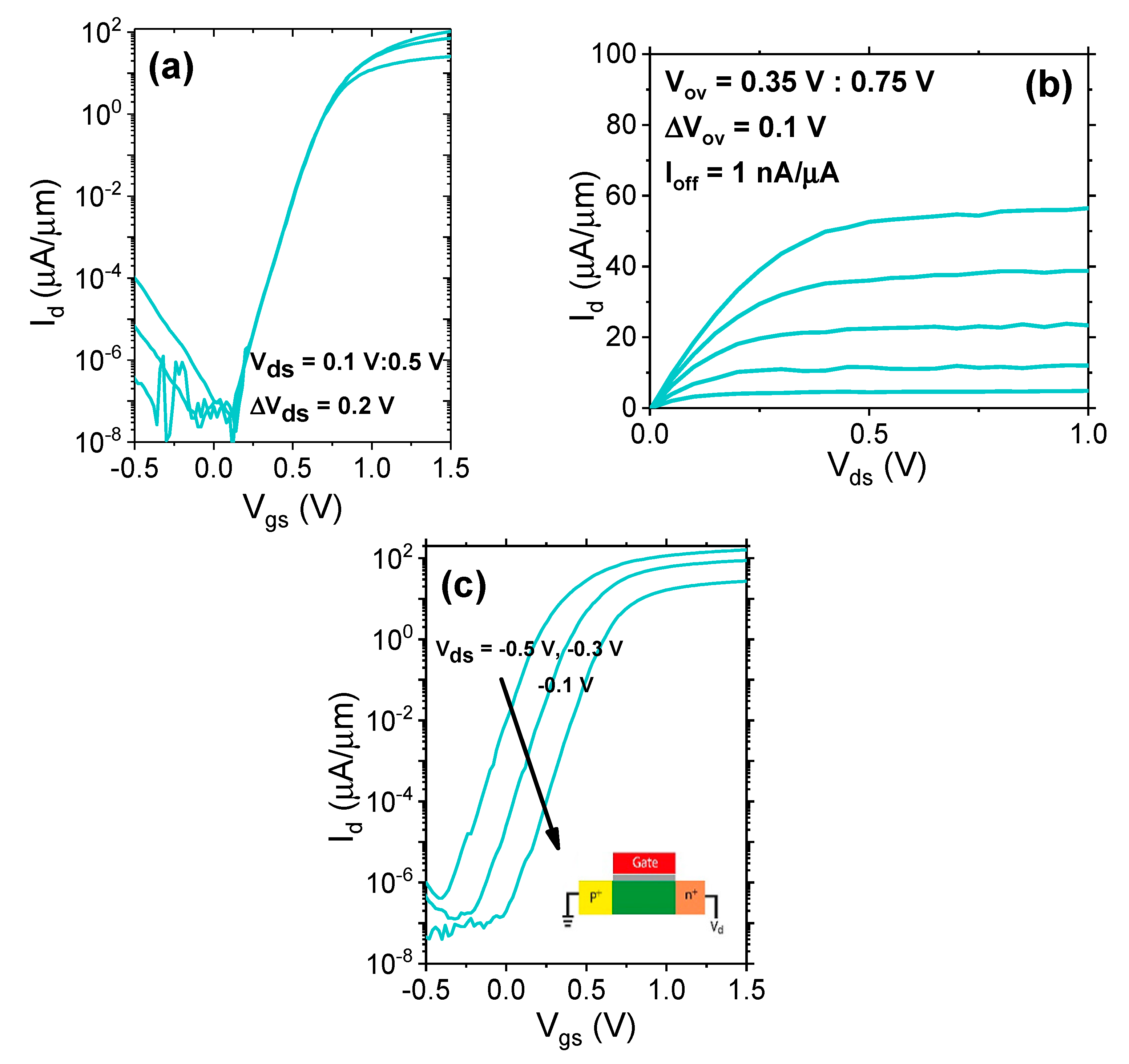
Thus, Set 3 of TFETs was fabricated with the aim to optimize the super-linear onset of n-TFET. In this case, 1 × 1015 cm−2 P+ ions at 3 keV and 1 × 1015 cm−2 B+ ions at 0.8 keV both without tilt (in normal direction) were implanted for source and drain, respectively. The dopants were activated at 500 °C for 10 s. This combination of implantation tilt, energy, and activation were chosen to achieve steeper boron junctions. Figure 5a,b shows the transfer and output characteristics of the n-TFET device. The output characteristics show very good linear behavior by increasing Vds as well as excellent current saturation. The latter is a key performance parameter for analog applications, for example, a current mirror. Moreover, the on current was also improved compared to the Set 2 devices, showing Ion = 15 µA/µm at Vov = Vgs − Voff = 0.5 V with an Ioff = 1 nA/µm. The average SS was also improved to 76 mV/dec over 4 orders of drain current Id. The minimum SS is still above 60 mV/dec, which could be attributed to the undesired effect of trap-assisted tunneling (TAT) caused by interface traps [14,15]. Figure 5c presents the Id-Vgs characteristics for the p-i-n diode forward biased with various Vd, as illustrated in the inset. The curves show typical forward p-i-n diode behavior—much higher currents than TFET and the current decreases with decreasing absolute Vd. This also provides evidence of the TFET operations for the results shown in Figure 5a,b. Table 1 summarizes the fabrication parameters and the device performance.
4. Conclusions
By proposing the advantage of a single nanowire over an array of nanowires in studying the effect of different process steps, we have investigated how ion implantation and dopant activation parameters impact the performance of strained silicon single NW GAA TFETs. The goal was to improve the TFETs in terms of Ion-current and average subthreshold swing. The best result was achieved for n-TFETs with ion implantation in the normal direction to the nanowire surface and dopant activation at a moderate temperature of 500 °C, as compared to the annealing temperature of 550 °C for p-TFETs. Such optimized n-TFETs deliver high Ion-currents of 15 µA/µm at Vdd = 0.5 V and a low average subthreshold swing of 76 mV/dec over 4 decades of drain current.
Author Contributions
K.N. fabricated and measured the devices and wrote the paper; S.T. performed the e-beam lithography; A.T. deposited the gate oxide and metal layers; S.M. and Q.-T.Z. contributed to the analysis of data and writing of the paper.
Acknowledgments
This work is partially supported by the BMBF project UltraLowPow (16ES0060K) and the European project E2SWITCH.
Conflicts of Interest
The authors declare no conflict of interest.
References
- Appenzeller, J.; Lin, Y.M.; Knoch, J.; Chen, Z.; Avouris, P. Comparing carbon nanotube transistors—The ideal choice: A novel tunneling device design. IEEE Trans. Electron Devices 2005, 52, 2568–2576. [Google Scholar] [CrossRef]
- Choi, W.Y.; Park, B.G.; Lee, J.D.; Liu, T.J.K. Tunneling field-effect transistors (TFETs) with subthreshold swing (SS) less than 60 mV/dec. IEEE Electron Device Lett. 2007, 28, 743–745. [Google Scholar] [CrossRef]
- Nah, J.; Liu, E.S.; Varahramyan, K.M.; Dillen, D.; McCoy, S.; Chan, J.; Tutuc, E. Enhanced-performance germanium nanowire tunneling field-effect transistors using flash-assisted rapid thermal process. IEEE Electron Device Lett. 2010, 31, 1359–1361. [Google Scholar] [CrossRef]
- Juang, M.-H.; Hu, P.-S.; Jang, S.-L. Formation of lateral SiGe tunneling field-effect transistors on the SiGe/oxide/Si-substrate. Semicond. Sci. Technol. 2009, 24, 25019. [Google Scholar] [CrossRef]
- Dewey, G.; Chu-Kung, B.; Boardman, J.; Fastenau, J.M.; Kavalieros, J.; Kotlyar, R.; Liu, W.K.; Lubyshev, D.; Metz, M.; Mukherjee, N.; et al. Fabrication, characterization, and physics of III-V heterojunction tunneling field effect transistors (H-TFET) for steep sub-threshold swing. In Proceedings of the 2011 International Electron Devices Meeting, Washington, DC, USA, 5–7 December 2011; pp. 33.6.1–33.6.4. [Google Scholar] [CrossRef]
- Knoll, L.; Richter, S.; Nichau, A.; Trellenkamp, S.; Schäfer, A.; Wirths, S.; Blaeser, S.; Buca, D.; Bourdelle, K.K.; Zhao, Q.-T.; et al. Strained silicon based complementary tunnel-FETs: Steep slope switches for energy efficient electronics. Solid State Electron. 2014, 98, 32–37. [Google Scholar] [CrossRef]
- Knoll, L.; Zhao, Q.T.; Nichau, A.; Trellenkamp, S.; Richter, S.; Schäfer, A.; Esseni, D.; Selmi, L.; Bourdelle, K.K.; Mantl, S. Inverters with strained Si nanowire complementary tunnel field-effect transistors. IEEE Electron Device Lett. 2013, 34, 813–815. [Google Scholar] [CrossRef]
- Luong, G.V.; Narimani, K.; Tiedemann, A.T.; Bernardy, P.; Trellenkamp, S.; Zhao, Q.T.; Mantl, S. Complementary Strained Si GAA Nanowire TFET Inverter With Suppressed Ambipolarity. IEEE Electron Device Lett. 2016, 37, 950–953. [Google Scholar] [CrossRef]
- Chen, C.-J.; Chen, Y.-N.; Fan, M.-L.; Hu, V.P.-H.; Su, P.; Chuang, C.-T. Impacts of work function variation and line-edge roughness on TFET and FinFET devices and logic circuits. In Proceedings of the SOI-3D-Subthreshold Microelectronics Technology Unified Conference (S3S), Millbrae, CA, USA, 6–9 October 2014; pp. 1–2. [Google Scholar] [CrossRef]
- Zhao, Q.-T.; Knoll, L.; Richter, S.; Schulte-Braucks, C.; Luong, G.V.; Blaser, S.; Schafer, A.; Trellenkamp, S.; Mantl, S. Strained silicon nanowire tunnel FETs and NAND logic. In Proceedings of the 12th IEEE International Conference on Solid-State and Integrated Circuit Technology (ICSICT), Guilin, China, 28–31 October 2014; pp. 1–4. [Google Scholar] [CrossRef]
- Knoll, L.; Schafer, A.; Trellenkamp, S.; Bourdelle1, K.K.; Zhao, Q.T.; Mantl, S. Nanowire and planar UTB SOI Schottky Barrier MOSFETs with dopant segregation. In Proceedings of the 13th International Conference on Ultimate Integration on Silicon (ULIS), Grenoble, France, 6–7 March 2012; pp. 45–48. [Google Scholar] [CrossRef]
- Sandow, C.; Knoch, J.; Urban, C.; Zhao, Q.T.; Mantl, S. Impact of electrostatics and doping concentration on the performance of silicon tunnel field-effect transistors. Solid State Electron. 2009, 53, 1126–1129. [Google Scholar] [CrossRef]
- De Michielis, L.; Lattanzio, L.; Ionescu, A.M. Understanding the Superlinear Onset of Tunnel-FET Output Characteristic. IEEE Electron Device Lett. 2012, 33, 1523–1525. [Google Scholar] [CrossRef]
- Verhulst, A.S.; Vandenberghe, W.G.; Leonelli, D.; Rooyackers, R.; Vandooren, A.; De Gendt, S.; Heyns, M.M.; Groeseneken, G. Tunnel Field-Effect Transistors for Future Low-Power Nano-Electronics. ECS Trans. 2009, 25, 455–462. [Google Scholar] [CrossRef]
- Der Agopian, P.G.; Martino, M.D.V.; Filho, S.G.D.S.; Martino, J.A.; Rooyackers, R.; Leonelli, D.; Claeys, C. Temperature impact on the tunnel fet off-state current components. Solid State Electron. 2012, 78, 141–146. [Google Scholar] [CrossRef] [Green Version]
Figure 1.
Fabrication process steps as well as schematics of the final device structure of the single nanowire (NW) tunnel field effect transistors (TFETs).
Figure 1.
Fabrication process steps as well as schematics of the final device structure of the single nanowire (NW) tunnel field effect transistors (TFETs).

Figure 2.
(a) Top view of a scanning electron microscope (SEM) image of a suspended silicon NW before gate fabrication process. (b) Side view of the final single NW TFET. It is clear that the gate metal completely wraps around the NW creating a gate-all-around (GAA) structure. The NW cross-section amounts to 35 nm × 10 nm.

Figure 3.
Measurement results of Set 1 devices. (a) Id-Vg transfer characteristics for p-TFETs annealed at two different activation temperatures. (b) Id-Vds output characteristics for the corresponding devices, showing the super-linear onset of the Id-Vds curves.
Figure 3.
Measurement results of Set 1 devices. (a) Id-Vg transfer characteristics for p-TFETs annealed at two different activation temperatures. (b) Id-Vds output characteristics for the corresponding devices, showing the super-linear onset of the Id-Vds curves.

Figure 4.
Measurement results of Set 2 devices: transfer characteristics Id-Vg for p-TFET (a), and n-TFET (b); Output characteristics Id-Vds for the corresponding devices (c,d). The p-TFET device shows a linear onset, indicating higher concentration of the n+/channel junction.
Figure 4.
Measurement results of Set 2 devices: transfer characteristics Id-Vg for p-TFET (a), and n-TFET (b); Output characteristics Id-Vds for the corresponding devices (c,d). The p-TFET device shows a linear onset, indicating higher concentration of the n+/channel junction.

Figure 5.
Measurement results of Set 3 devices: (a) Transfer characteristics Id-Vg of the optimized n-TFET, (b) corresponding output characteristics Id-Vds of the fabricated device showing good saturation and linear onset. The device shows very high on-currents of 15 µA/µm at Vdd = 0.5 V. (c) Forward biased Id-Vgs characteristics of the p-i-n diode, showing typical forward I-V curves for the diode.


Table 1.
A summary of different implantation and activation parameters and the corresponding results. Ion was extracted at Vds = Von = Vg − Voff = −0.5 V for Ioff = 1 nA/µm. SSavg is the average subthreshold swing from the minimum of drain current for 4 orders of magnitude at Vds = 0.1 V.
Table 1.
A summary of different implantation and activation parameters and the corresponding results. Ion was extracted at Vds = Von = Vg − Voff = −0.5 V for Ioff = 1 nA/µm. SSavg is the average subthreshold swing from the minimum of drain current for 4 orders of magnitude at Vds = 0.1 V.
| Set | Implantation | Activation | Ion µA/µm | SSavg mV/dec | Linear Onset |
|---|---|---|---|---|---|
| pTFET (Set1) | P 1 × 1015 cm−2 45° | 500 °C | 8.52 | 84 | No |
| B 5 × 1014 cm−2 45° | 20 s | ||||
| pTFET (Set1) | P 1 × 1015 cm−2 45° | 600 °C | 3.94 | 126 | No |
| B 5 × 1014 cm−2 45° | 20 s | ||||
| pTFET (Set2) | P 5 × 1015 cm−2 45° | 550 °C | 2.41 | 102 | Yes |
| B 1 × 1015 cm−2 45° | 10 s | ||||
| nTFET (Set2) | P 5 × 1015 cm−2 45° | 550 °C | 0.78 | 153 | No |
| B 1 × 1015 cm−2 45° | 10 s | ||||
| nTFET (Set3) | P 1 × 1015 cm−2 0° | 500 °C | 15 | 76 | Yes |
| B 1 × 1015 cm−2 0° | 10 s |
© 2018 by the authors. Licensee MDPI, Basel, Switzerland. This article is an open access article distributed under the terms and conditions of the Creative Commons Attribution (CC BY) license (http://creativecommons.org/licenses/by/4.0/).
Share and Cite
MDPI and ACS Style
Narimani, K.; Trellenkamp, S.; Tiedemann, A.; Mantl, S.; Zhao, Q.-T. Strained Silicon Single Nanowire Gate-All-Around TFETs with Optimized Tunneling Junctions. Appl. Sci. 2018, 8, 670. https://doi.org/10.3390/app8050670
AMA Style
Narimani K, Trellenkamp S, Tiedemann A, Mantl S, Zhao Q-T. Strained Silicon Single Nanowire Gate-All-Around TFETs with Optimized Tunneling Junctions. Applied Sciences. 2018; 8(5):670. https://doi.org/10.3390/app8050670
Chicago/Turabian StyleNarimani, Keyvan, Stefan Trellenkamp, Andreas Tiedemann, Siegfried Mantl, and Qing-Tai Zhao. 2018. "Strained Silicon Single Nanowire Gate-All-Around TFETs with Optimized Tunneling Junctions" Applied Sciences 8, no. 5: 670. https://doi.org/10.3390/app8050670
Note that from the first issue of 2016, this journal uses article numbers instead of page numbers. See further details here.