Thermal Energy Diffusion Incorporating Generalized Einstein Relation for Degenerate Semiconductors


Department of Electronics Engineering, Incheon National University, Incheon 22012, Korea
Appl. Sci. 2017, 7(8), 773; https://doi.org/10.3390/app7080773
Submission received: 13 June 2017
/
Revised: 18 July 2017
/
Accepted: 25 July 2017
/
Published: 31 July 2017
Abstract
:The currently used generalized Einstein relation for degenerate semiconductors with isotropic nonparabolic energy bands produces physically improper results, as well as losing numerical accuracy for large values of nonparabolicity parameters at room temperature. Therefore, a new generalized Einstein relation (a macroscopic equation and a formula) is derived from the semiclassical momentum balance equation based on a drift-diffusion approximation, by introducing a new concept of the effective temperature of a carrier gas for generalization of the classical kinetic theory for nonideal gases of carriers in semiconductors. The proposed formula takes into account the carrier thermal energy diffusion effect completely, so that it can accurately reflect the effect of band nonparabolicity on the ratio of the diffusion coefficient to the mobility for carriers in degenerate semiconductors. From the results evaluated with the formula, new and critically important nonparabolicity effects are observed. It is shown that the new generalized Einstein relation is valid for applied electrical fields of the full linear regime. In addition, useful figures are also presented, from which the ratio of the diffusion coefficient to mobility, as well as the Fermi energy, can be easily determined from the electron concentration, or doping density, for a given semiconductor material.
1. Introduction
The diffusion coefficient (D) and mobility (μ) of carriers are critically important fundamental transport parameters for describing the properties of carrier transport in semiconductor devices and materials, and are interconnected to each other through a factor by the Einstein relation. Due to the theoretically sound interconnection between them, the diffusion coefficients are commonly determined from the mobility using the Einstein relation, which therefore plays a key role in semiconductor analysis and device design. However, the values of the factor, i.e., the D/μ ratio, are generally given differently depending on the carrier concentration in an energy band and the electronic structure of the energy band, as well as the carrier temperature.
The Einstein relation was initially derived for particles of Brownian motion based on the ideal gas law and Fick’s law of diffusion [1]. Therefore, this classical Einstein relation is valid only for particles that obey Maxwell–Boltzmann statistics and have the same mass. Only in such a case, the D/μ ratio is given by a constant, and is particularly equal to the value of the thermal voltage for charged particles developing an electric field.
The conventional Einstein relation derived for nondegenerate semiconductors based on the use of Maxwell-Boltzmann statistics with the assumption that the carrier effective mass is constant, i.e., the energy band structure is parabolic, is given by:
where kB is the Boltzmann constant; TL denotes the temperature of the semiconductor system in thermal equilibrium, i.e., the lattice temperature (or the carrier temperature) in K; and q is the positive electronic charge. Even though Equation (1) can be derived separately for carriers in semiconductors by applying the principle of detailed balance to the current equation, or in other ways, its theoretical basis is essentially the same as the classical Einstein relation stated above (the inclusion of q in Equation (1) is due to the charge of a carrier).
On the bases of Fermi-Dirac statistics and the parabolic energy band assumption, a general Einstein relation that is valid for degenerate, as well as nondegenerate, semiconductors was derived earlier using the concept of the average kinetic energy of electrons in thermal equilibrium, which is given by [2]
and it was shown that the D/μ ratio for electrons is approximately equal to (2/3) /q, where is the Fermi energy (FE), and refers to the conduction band (CB) bottom energy, for metals and strongly degenerate semiconductors. The Einstein relation for carriers in semiconductors was also investigated using an expression () derived in terms of the chemical potential, , and it was shown that in general, the D/μ ratio depends on carrier concentration, rather than being constant, and is proportional to n2/3 for highly degenerate semiconductors [3]. By employing the principle of detailed balance, an expression equivalent to Equation (2a), but simpler, was also derived, such as [4,5]:
In these equations, F1/2(ηc) and F−1/2(ηc) refer, respectively, to Fermi-Dirac integrals of order 1/2 and −1/2, which is given as a function of the reduced Fermi energy defined by:
Note that Equation (2b) can be obtained from Equation (2a) if the recurrence relation of Fermi-Dirac integrals is utilized. The former simpler Equation (2b) is commonly referred to as the generalized Einstein relation for electrons, but it is valid only for semiconductors having parabolic energy bands. This generalized Einstein relation is often formulated in a different form, such as [6,7,8]:
where n is the electron concentration. However, this form is equivalent to Equation (2b), due to the following identities:
where Nc denotes the effective density of states (DOS) for parabolic CB cases, and the recurrence property of Fermi-Dirac integrals has been used.
The experimentally established Fick’s law asserts that the diffusive flux of particles at a local spatial point is simply proportional to the spatial gradient of the particle concentration. In this macroscopic law, the proportional parameter (the diffusion coefficient) represents the average property of a particle for diffusion. However, we see in Equation (2b) that, due to the microscopic property of carriers’ quantum mechanical behavior, the additional factor F1/2(ηc)/F−1/2(ηc) appears when Fermi-Dirac statistics are adopted. This causes the D/μ ratio, representing an average property, to depend on a spatial position, even though all of the electrons have the same effective mass and are subject to the same macroscopic temperature.
The direct reason for the appearance of the additional factor is, of course, due to the carrier concentration being given by a Fermi-Dirac integral in Fermi-Dirac statistics. However, the underlying physical reason for its appearance beyond such a somewhat mathematical reason has not yet been addressed, and is clarified in detail in the following. Let us consider a fixed number N of degenerate electrons distributed in a certain parabolic CB. We assume that they have been restricted to be redistributed over energy states according to Maxwell-Boltzmann statistics by some external means. Recall that Maxwell-Boltzmann statistics permits any number of electrons to occupy the same quantum (spin) state [9]. Now, if we remove the external restricting condition, it is expected that a large fraction of the electrons sharing the same quantum states with a higher probability of occupation at a lower energy will jump over to higher-energy empty states to accommodate Pauli’s exclusion principle, the key law in Fermi-Dirac statistics. This will give rise to an increase in the average kinetic energy of electrons from the average value that resulted from the Maxwell-Boltzmann statistics, essentially leading to a larger kinetic pressure of the electron gas. Therefore, for a given mobility, the diffusivity of the N electrons will be larger due to their greater energetic kinetic motion, on average. In fact, this effect is reflected by the additional factor. Note that the factor F1/2(ηc)/F−1/2(ηc) is always larger than unity for any values of ηc. Thus, for a parabolic energy band, a larger value in the D/μ ratio is always generated even for the nondegenerate condition (ηc < −3) when Fermi-Dirac statistics is applied.
In semiconductors, nonparabolicity always exists in their energy band structures. The nonparabolicity effect on carrier transport is technically important, particularly for direct-bandgap compound semiconductors with high electron mobility, since they can have significant nonparabolicity in their central conduction valleys, which feature isotropic constant surfaces of energy. This necessitates a more generalized Einstein relation, beyond Equation (2b) or Equation(4), which can properly take into account the nonparabolicity effect.
Using an approximate Kane’s dispersion relation [10,11], a more generalized Einstein relation for degenerate semiconductors with nonparabolic energy bands was also derived earlier [12], and the result has often been utilized [13,14,15]. This existing generalized Einstein relation for electrons in nonparabolic CBs is given by:
where α is the nonparabolicity parameter, usually expressed in the unit of eV−1, for the isotropic CB; and F3/2(ηc) is the Fermi-Dirac integral of order 3/2. Note that Equation (6) was obtained by assuming that α() << 1, where is the electron energy, in order to simplify the density integral (refer to Equation (14)) in a closed form by the binomial approximation.
Concerning the formula of Equation (6), however, two theoretically serious defects are pointed out here: (1) due to the adoption of the binomial approximation for the derivation, it produces large errors for large values of α or TL (see Figure 1); and (2) in the nondegenerate condition, it reduces to the conventional Einstein relation, Equation (1), derived for parabolic energy bands, since all of the Fermi–Dirac integrals are almost equal in value if ηc < −3. However, this aspect is physically improper. The reason is explained in the following. Let us consider two different cases of CBs, in which both bands have the same value of mc (the electron effective mass at the band bottom), but one is parabolic (α = 0) and the other is nonparabolic (α > 0). For the case of α = 0, the DOS in three-dimensional k-space (momentum space) is uniformly equal throughout the space. However, for the case of α > 0, the DOS increases continuously as the magnitude of k increases from zero (the energy minimum point) [16], since the energy-dependent effective mass for electrons increases continuously as the energy increases. Therefore, for a given FE, the average kinetic energy of electrons is always given more largely in the case of α > 0, resulting in a larger diffusivity of electrons for a fixed mobility, as already explained above. In other words, if nonparabolicity exists in an energy band, we always have a larger D/μ ratio for any values of ηc, i.e., even for the nondegenerate condition, than that expected by the parabolic band approximation.
If the binomial approximation is applied for the density integral, the electron concentration can be approximated by:
Substituting this equation into Equation (4), we simply obtain Equation (6). Therefore, the existing generalized Einstein relation for nonparabolic energy bands is a simple modification of the carrier concentration to the generalized Einstein relation for parabolic energy bands, so that it disregards the carrier thermal energy diffusion effect arising from the thermal kinetic motion of carriers. The consequence is that it produces a physically improper D/μ ratio, as can be verified in Section 4.
The formulas of the Einstein relation (1), (2b), (4), and (6) were derived in thermal equilibrium or near-equilibrium conditions by various approaches, typically based on the principle of detailed balance or the Boltzmann transport equation (BTE), respectively. In the present paper, a new, much more generalized Einstein relation for degenerate semiconductors with isotropic nonparabolic energy bands is derived rigorously based on the semiclassical momentum balance equation that was obtained from the BTE, by assuming a near-equilibrium transport condition, as specified in Section 3, and formulated to be utilized for semiconductors, particularly with accuracy for direct-bandgap semiconductors where their lowest CB structures can be approximated by Kane’s dispersion relation. It is known that Kane’s band model is not valid for high electron energies (e.g., above about 0.5 eV from in the case of Si) [16]. However, it is presented in Section 4 that the D/μ ratio for conduction electrons in a semiconductor is not affected generally by the electronic property of a band structure above 0.4 eV from the CB edge at room temperature.
The derivation of the new formula employs a new concept of the effective temperature of a carrier gas for the generalization of the classical kinetic theory, which is introduced in the present paper for the first time. Therefore, it is first necessary to describe this concept prior to the derivation. According to the equipartition theorem, the average translational kinetic energy, w, of a carrier gas in a semiconductor in thermal equilibrium conditions is related to the carrier temperature or the semiconductor lattice temperature TL as:
However, it is essential to realize that, strictly speaking, the factor 1/2 in this equation holds only for ideal gases, such that: (1) all of the particles have the same mass (e.g., electrons in parabolic energy bands); and (2) there is no interaction among particles, except during elastic collisions (Maxwell–Boltzmann statistics is applicable, i.e., particles are not subject to Pauli’s exclusion principle). Therefore, for carriers in degenerate semiconductors with parabolic energy bands or carriers in semiconductors with nonparabolic energy bands, the two conditions of (1) and (2) do not hold, so that Equation (8) is not valid. Generally, the average kinetic energy w of a gas of particles is a function of particle temperature and particle concentration. For ideal gases, the energy is a function of particle temperature only, and the factor 1/2 holds. Otherwise, this factor is given differently. In thermal equilibrium, the carrier temperature must be equal to the semiconductor lattice temperature. Therefore, by introducing the effective temperature of a carrier gas, TE, for the generalization of the classical kinetic theory for nonideal gases of carriers, the equipartition theorem of Equation (8) can be modified to the following form of a generalized expression:
In the following section, the effective temperature of electrons in nonparabolic energy bands is thus derived first, and then the new generalized Einstein relation is derived and formulated in the subsequent section.
2. The Effective Temperature of Electrons in Thermal Equilibrium
Kane’s dispersion relation for isotropic nonparabolic CBs is given by:
where ħ is the reduced Plank’s constant; k is the magnitude of the wave vector k; and mc denotes the electron effective mass at , as defined previously. The electron concentration and the thermal kinetic energy density of electrons can be evaluated simultaneously from the following density integral moment equation by introducing a moment parameter λ:
where f(k) is the probability function for an electron near k, and the integration is over all k-space within the band (in the first Brillouin zone). If λ = 0, Equation (11) yields the electron concentration, and if λ = 1, the thermal kinetic energy density. In thermal equilibrium, the distribution function f(k) is given by the isotropic Fermi–Dirac distribution function. Therefore, by substitution, we have:
Differentiating Equation (10) with respect to k gives:
Substitution of Equations (10) and (13) into Equation (12) yields:
where h is Plank’s constant and a dimensionless parameter β = αkBTL has been introduced. The integration variable is defined by x = ()/(kBTL), and Nc, the effective DOS, is given by:
In the present work, the square-root part involved in the integral of Equation (14) is approximated by choosing a suitable fitting number for the coefficient of the linear term empirically based on the following expansion property:
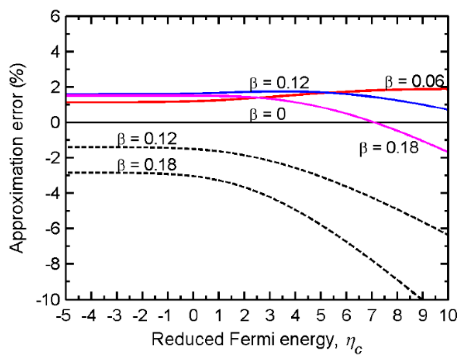
The accuracy of this empirical approximation for Equation (14) has been numerically calculated in the case of λ = 1 (larger errors are resultant for λ = 1 than λ = 0), and the results are depicted in Figure 1. Note that the approximation is quite accurate with a maximum error of less than 2% over a very wide range of ηc for the extensive variation of β values. In the same figure, calculated errors induced by the binomial approximation are also depicted in dashed curves typically for β = 0.12 and 0.18 for comparison. As shown, the errors of this approximation increase largely with the FE for ηc > 3, and in particular, the error is significantly larger for the large value of β = 0.18 at Fermi energies of ηc > 5.
By using the empirical approximation, the density moment equation is evaluated as follows:
By letting λ = 0 and λ = 1, the electron concentration and the thermal kinetic energy density are obtained, respectively, as:
and
where
for the Fermi–Dirac integral of order j.
Finally, from Equations (9), (18) and (19), the effective temperature of electrons for nonparabolic energy bands is obtained as:
From this equation, it is worth noting that, for nonparabolic CBs where β > 0, we always have TE > TL for any values of ηc. For parabolic CBs where β = 0, Equation (21) gives TE ≈ TL for the nondegenerate condition and TE = F3/2(ηc)/F1/2(ηc)TL generally.
3. Derivation of the New Generalized Einstein Relation
The derivation uses the semiclassical momentum balance equation that was derived from the BTE by the method of moments for describing the macroscopic transport properties of electrons in a single conduction valley with a nonparabolic energy band structure (for Equation (23), refer to Appendix A) [13,17]:
and
where t is the time; P, v, and T are the momentum density, the average velocity (i.e., the drift velocity), and the electron temperature tensor, respectively; E is the electric field; and vo represents a drift velocity equal to the electron velocity at the wave vector ko in k-space (ko and (w) are defined following Equations (24) and (25), respectively). The variable Q thus represents the total kinetic energy density tensor that has combined three tensor quantities: the first quantity corresponds to a kinetic pressure tensor of the electron gas due to the random thermal motion of electron particles deviated from their average velocity in velocity space [17], or their average momentum in k-space (see Equation (25)); the second corresponds to a kinetic energy density tensor associated with the group drift motion in real space; and the third corresponds to a kinetic energy density tensor appearing due to the difference in magnitude between the two velocities of v and vo. For parabolic energy bands, v equals vo, so that this density tensor becomes zero. In particular, the divergence of the second tensor quantity represents the rate of local outflow of the momentum density, and is responsible for the appearance of a velocity convection term in the momentum balance equation when expressed in terms of drift velocity. This convection term is usually neglected in high-field transport device simulations for numerical convenience. If the total energy density tensor Q is written in matrix form, then Qαβ = nkBTαβ + vαPβ + Pα(vβ − voβ) for α and β = x, y, z (space coordinates) with Tαβ, vα, vβ, Pα, Pβ, and voβ the corresponding components of T, v, P, and vo, respectively.
The collision term in Equation (22) accounts for the rate of change in momentum density due to carrier scattering. Under the usual relaxation-time approximation [18], this term becomes −P/τm(w), where τm(w) is the average momentum relaxation time, so that Equation (22) in the steady-state condition is simplified to
where μ = qτm(w)/m*(w) is the mobility, with m*(w) being the average conductivity effective mass (the mobility is thus dependent on w, but a simple notation has been used). The energy-dependent parameters τm(w) and m*(w) are usually determined by Monte Carlo simulations in stationary transport conditions. The momentum density and the average velocity are related to each other through the average conductivity effective mass by P = nm*(w)v. In addition, the momentum density is given by P = n<ħk> = nħko, where the angle brackets mean the average over all of the electrons, so that ko denotes the weighted average wave vector in k-space. The temperature tensor is obtained as (see Appendix A):
where mk = mc(1 + 2α), which is the electron mass associated with the group velocity of an electron wave packet at the state of k [13,16,19]. The magnitude of m*(w) is not equal to that of <mk> = mc(1 + 2αw), which is defined by (w), for nonparabolic energy bands, and lies between the magnitudes of (w) and mc(1 + 2αw)3, depending on the electric field strength [20]. At low applied electric fields, m*(w) and (w) are approximately equal in magnitude in stationary transport conditions.
In order to derive the new generalized Einstein relation strictly, a near-equilibrium transport (NET) condition is assumed, such that at each local point of a semiconductor region, the average drift kinetic energy of carriers is negligibly very small so that their average kinetic energy, w, does not change perceivably by an applied electric field from the value of their average thermal kinetic energy obtained in near-equilibrium, i.e., the average thermal kinetic energy that is given for carriers of the same concentration in thermal equilibrium. In the following, this thermal energy will be referred to as the equilibrium average thermal kinetic energy, and the corresponding nondisplaced distribution function of carriers as the equilibrium distribution function. It should be mentioned that in semiconductor devices, the carrier concentration in near-equilibrium generally differs and can deviate significantly from its value in thermal equilibrium when an electric field has been applied. A typical example is the case of carriers being injected from the junction into an opposite-type semiconductor region and transported diffusively as minority carriers in a p-n junction diode. The NET condition assumed then means collaterally that: (1) the carriers practically retain thermal equilibrium with the lattice during their transport by releasing their energy gained from the electric field to the lattice rapidly through scattering, so that the transport of carriers is stationary (i.e., under a local-transport condition); (2) since the carriers are little heated and hence their distribution function does not expand perceivably by a local electric field, it is only displaced in k-space in proportion to the strength of the field (generally, a local driving force, electric or diffusive), so that the transport characteristic of carriers is linear (i.e., carrier velocity response to a local driving force is linear); and (3) since the average drift kinetic energy of carriers is so small, the displacement of the distribution function is not large, so that the carrier concentration can be approximated properly by using the equilibrium distribution function of carriers centered at k = 0 for isotropic nonparabolic energy bands where the DOS is distributed nonuniformly in k-space. The reason is associated with the spherical symmetricity existing in both the structure of the energy band and the distribution function of the carriers, which causes the average of the antisymmetric part of the carrier distribution in k-space to be approximately zero in the NET condition. Note that for parabolic energy bands, the carrier concentration is not changed by any mere displacement of the distribution function in k-space due to a uniformly distributed DOS in k-space. Thus, it should be noted that the generalized Einstein relation to be derived in this section is invalid if any of these detailed three subconditions of the NET condition is not satisfied.
Therefore, it follows from the assumption that: (1) all of the drift kinetic energy tensor components of vαPβ, as well as Pα(vβ − voβ), can be neglected; and (2) all of the non-diagonal components of T, i.e., Tαβ with α ≠ β, completely vanish, due to the existence of the isotropic symmetricity in both the band structure and the distribution function in the NET condition. In addition, all of the diagonal components of T, i.e., Tαβ with α = β, are almost equal in magnitude (not exactly equal for nonparabolic energy bands due to a displacement of the distribution function). As a result, a scalar electron temperature T can be defined justly so that T = Tδ, where δ is the unit dyad. From these results of (1) and (2), Equation (24) reduces to the following drift–diffusion equation:
where
In the NET condition, the average thermal kinetic energy remains the same as the equilibrium average thermal kinetic energy, so that the electron temperature T becomes dependent only on the local FE, which in turn uniquely determines the electron concentration, or vice versa. Therefore, Q = Q(n,T) becomes a function of only one independent variable, ηc. In other words, Q = Q(ηc(n(x,y,z))). Consequently, the application of the chain rule for differentiation to Equation (26) results in:
where
and
Note that, in Equation (30), the electron temperature T has been reduced to the effective temperature of electrons in thermal equilibrium, TE, due to the fact that T ≈ TE under the NET condition, and W is the total thermal kinetic energy density in thermal equilibrium, as defined in Section 2.
Equation (29), including Equation (30), is the new, much more generalized, macroscopic equation of the Einstein relation which can take into account the effect of thermal energy diffusion of carriers completely for degenerate semiconductors with isotropic nonparabolic energy bands. It is worth noting that this new generalized macroscopic equation reduces to Equation (1), the conventional Einstein relation for nondegenerate semiconductors with parabolic energy bands, for TE = TL, and also to Equation (4), or (2b), the generalized Einstein relation for degenerate semiconductors with parabolic energy bands, for TE = F3/2(ηc)/F1/2(ηc)TL and n = NcF1/2(ηc), since dQ/dηc = kBTLn then.
In the NET condition, the concentration n is approximately equal to the concentration value given by the equilibrium distribution function of carriers for an arbitrary value of the FE (generally quasi-FE), as described in subcondition (3). Therefore, substituting Equations (18) and (21), or Equation (19), into Equations (29) and (30) yields the following new generalized formulation of the Einstein relation for electrons in isotropic nonparabolic energy bands:
where the recurrence property of Fermi–Dirac integrals has been used such that:
For β = 0, the new formula reduces to Equation (2b), as well as Equation (1) in the nondegenerate condition. The corresponding generalized macroscopic equation and formula for valence holes in an isotropic nonparabolic band can be written directly from Equations (29)–(31). Equation (31) contains several Fermi–Dirac integrals, but they can be evaluated comfortably using a computer software package for mathematics. In addition, analytical expressions for approximating all of these integrals in a convenient form with reasonable accuracy is obtained in Reference [21]. Also note that in the nondegenerate condition, the Fermi-Dirac integrals included in both the numerator and denominator in Equation (31) are almost canceled, resulting in the following simple expression of the D/μ ratio that does not depend on the FE:
In other words, in the nondegenerate condition, the population of carriers over energy states in an energy band is not dense, so that Maxwell–Boltzmann statistics can be used as a very good approximation.
The validity limit of the new generalized macroscopic equation and formula for applied electric fields is discussed. Monte Carlo simulations performed for bulk materials at TL = 300 K show that the average electron energy (or the electron temperature) remains almost constant up to an electric field strength E = 2 kV/cm for GaAs [22], and E = 3 kV/cm for InP [23]. The doping densities of the materials were ND = 2 × 1017 cm−3 and ND = 1017 cm−3, respectively. The drift velocity for E = 2 kV/cm is v = 9 × 106 cm/s for the former case, and v = 9.6 × 106 cm/s for the latter, when calculated by v = μE (with μ = 4500 cm2/V-s for GaAs and μ = 3200 cm2/V-s for InP). It has been shown by calculations that the ratio of the drift kinetic energy, m*(w)v2/2, to the average thermal kinetic energy in thermal equilibrium, which is equal to 3kBTE/2, is negligibly small and less than 5% in both cases. This fact is in agreement with the assumption adopted in the derivation. Such a theoretical analysis indicates that the new macroscopic equation and formula can be valid for applied electric fields up to the upper velocity and field bounds of the linear regime (in the velocity-field relation) for conduction electrons of direct-bandgap semiconductors (v < 107 cm/s due to possible velocity overshoot). In this type of semiconductor, which usually features high electron mobility, the mean thermal velocity (vth) of electrons is commonly large due to their small effective mass (typically, for GaAs vth ≈ 4.5 × 107 cm/s in the nondegenerate condition at room temperature), so that the upper velocity bound of the linear regime is generally high for direct-bandgap semiconductors.
The generalized Einstein relation expressed by the macroscopic equation and the formula is dependent only on the spatial variation of the FE, i.e., the carrier concentration, and independent of the electric field. Therefore, the validity limit discussed above for direct-bandgap semiconductors generally holds for other types of semiconductors as well (of course, in the validity limits of isotropic nonparabolic band approximations). Since it has been derived on the basis of the BTE, its applications should be limited within the validity limits of the BTE. Note that this equation is valid only when the spatial variation of the potential in a semiconductor device is slow on the scale of the De Broglie wave length, which is typically 10 to 20 nm [16]. Therefore, for a small scaled device where the carrier concentration changes rapidly with position, the BTE itself is invalid.
4. Evaluation Results and Discussions
4.1. General Cases
The D/μ ratios for various values of β have been calculated numerically for electrons using Equation (31), and the results are plotted as a function of the reduced FE in Figure 2. The range of β values was decided in due consideration of the range of variation of α values of the major important semiconductors at room temperature. Note that if β > 0, the D/μ ratio is always larger than kBTL/q even for the nondegenerate condition, as reasoned in connection with Equation (6) in Section 1. Several important features noted are: (1) band nonparabolicity causes the D/μ ratios to always increase for any given FE; (2) for a given material, the D/μ ratio is constant and not dependent on the FE in the nondegenerate condition (ηc < −3), whereas it is linearly dependent on the FE for ηc > 3 (to be defined as the high degenerate condition in the following); (3) the relative amount of the nonparabolicity effect on the D/μ ratio is largest in the nondegenerate condition for a given material (however, it should be noted that this is the case only when the D/μ ratio is plotted as a function of the FE). In particular, for the large value of β = 0.18, the D/μ ratio is noted to increase significantly by 1.35 times in the nondegenerate condition; and (4) the D/μ ratios, including the case of parabolic energy bands (β = 0), increase a very large amount with increasing FE in the high degenerate condition. This indicates that the quantum mechanical effect of electron degeneracy on the D/μ ratio is very large for a highly degenerate electron gas.
In the same figure, the D/μ ratios calculated for electrons using the existing formula Equation (6) are also plotted typically for β = 0.06 (dashed curve 1) and β = 0.18 (dashed curve 2). It is worth noting that there are substantial differences in value between the results of the new formula and the existing formula. The results of the existing formula show that the D/μ ratios are not affected by the amounts of band nonparabolicity in the nondegenerate condition. An additional physically improper aspect is that band nonparabolicity causes the D/μ ratios to decrease quite significantly below the values obtained for β = 0 (parabolic energy band case), even for the small value of β = 0.06, in the high degenerate condition.
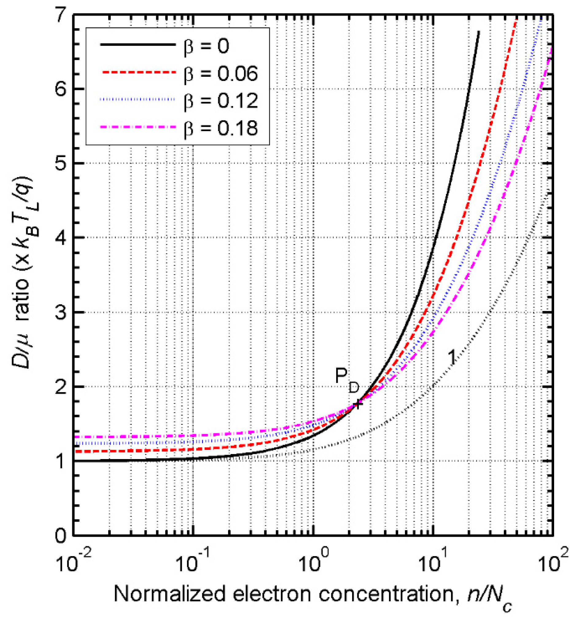
In Figure 3, the D/μ ratios for various values of β are plotted as a function of the electron concentration that has been normalized to the effective DOS, Nc. This figure shows a quite interesting feature, such that there exists a point, designated by PD, near which all of the curves of the D/μ ratios come to cross, and thus all have nearly the same value. The crossover of these curves arises near the point of D/μ = 1.77kBTL/q and n = 2.33Nc. This means that, for semiconductors with isotropic nonparabolic CBs, when the electron concentrations are equal to the value of 2.33Nc, the D/μ ratios for conduction electrons are always nearly equal to the value of 1.77kBTL/q, irrespective of the degree of nonparabolicity of their CBs. The corresponding Fermi energies to this value of D/μ are noted to be approximately between 0.5kBTL/q [eV] (ηc = 0.5) and 1.5kBTL/q [eV] (ηc = 1.5) when measured from the band bottom energy (refer to Figure 2).
In the figure, the D/μ ratio calculated for electrons with the existing formula, typically for β = 0.18, is also plotted with the curve 1 (dashed). The D/μ ratios for the other different values of β are not shown in the figure, but their values are obtained between the curve for β = 0 and the curve 1. Therefore, no crossover point, such as PD, is obtained with the existing formula.
It is shown in Figure 3 that, when the electron concentration is larger than 2.33Nc, the D/μ ratios increase considerably with increasing electron concentration, whereas when it is smaller than 2.33Nc, they do not change considerably. Especially when n < 0.1Nc, the D/μ ratios are constant and do not vary with the electron concentration (as in the nondegenerate condition of ηc < −3). It is quite interesting to note for a given material that for n < 2.33Nc, band nonparabolicity causes the D/μ ratio to increase (property 1), but for n > 2.33Nc, it causes the D/μ ratio to decrease (property 2). In Section 1, it was explained that a larger value of β always leads to a larger value of the D/μ ratio for a given FE. In the nondegenerate condition (ηc < −3 or n < 0.1Nc), the D/μ ratio is always constant, not depending on the FE and therefore not depending on the electron concentration. Therefore, we observe property 1 for n < 2.33Nc. The reason for property 2 is complicated, but can be explained as in the following. The DOS decreases as the value of β decreases. Therefore, if the CB is strongly degenerated by a very large concentration of electrons, the FE is required to increase considerably inside of the band in order for the very large concentration of electrons to be accommodated within the band if the value of β is small. As a result, the band will be populated by electrons up to a high energy state for a small value of β due to the increased FE. This will eventually give rise to a large average kinetic energy of electrons, so that the diffusivity of electrons will be increased substantially, if constant mobility is assumed. Therefore, as noted in Figure 3, a substantial increase in the D/μ ratio is possible, especially when β = 0, for a very large electron concentration. It is very important to note that the nonparabolicity effect on the D/μ ratio can be quite substantial even for a small value of β at a very large carrier concentration. In other words, if a semiconductor material is heavily doped, the parabolic band approximation can lead to a very large error in the D/μ ratio.
The electron concentration dependencies of the diffusion coefficient and the FE for a given semiconductor material can be easily determined from Figure 2 and Figure 3. In other words, we can find the value of the D/μ ratio and thus the value of the diffusion coefficient from Figure 3 with known values of n (or ND for homogeneous materials with dopants fully ionized), Nc, μ, and β, and thereafter the FE value also from Figure 2.
4.2. Specific Cases
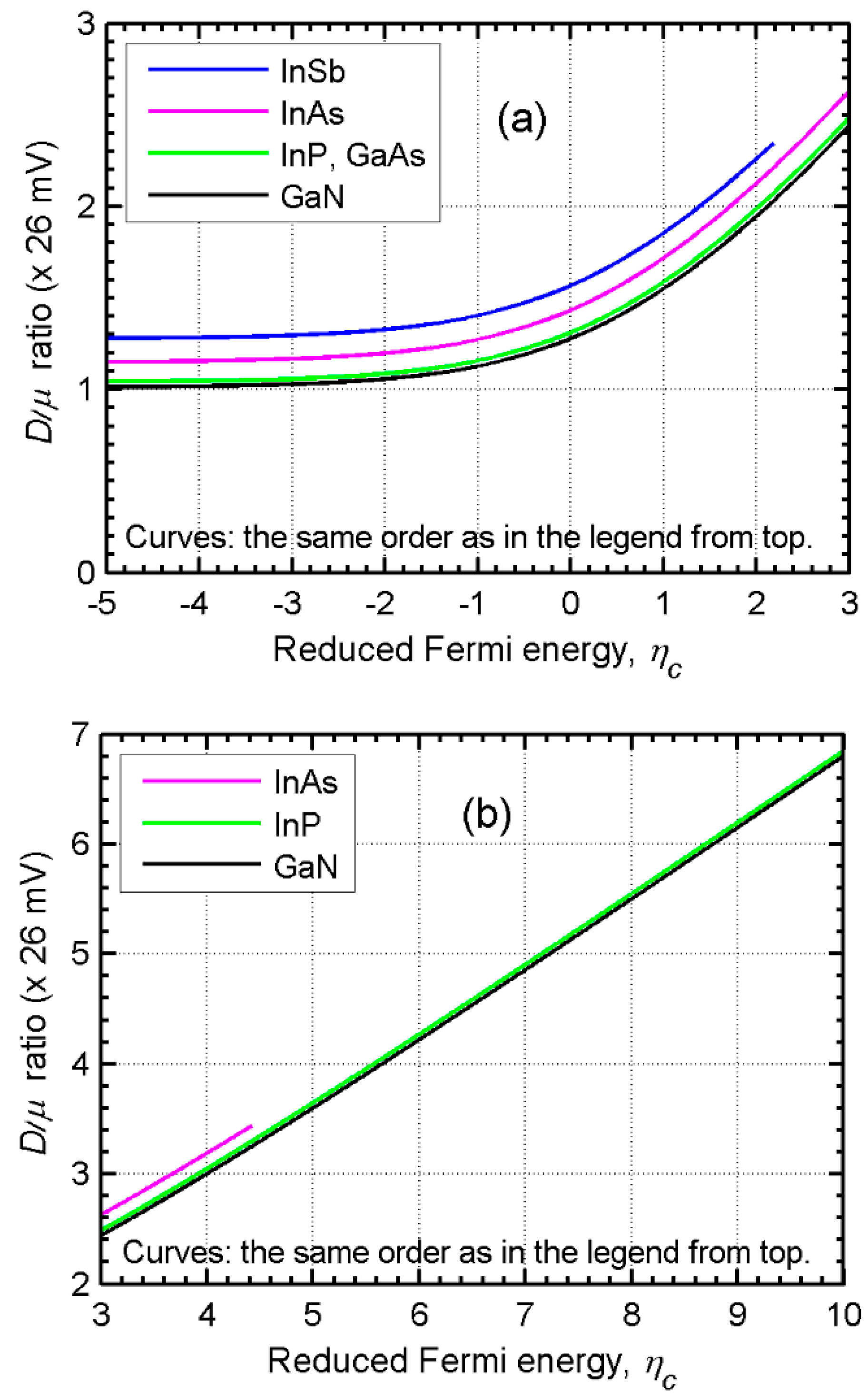
The D/μ ratios for conduction electrons at room temperature (TL = 300 K) in common direct-bandgap compound semiconductors have been calculated specifically using Equation (31), and the results are presented as a function of the reduced FE in Figure 4, and also as a function of the electron concentration in Figure 5 (replotted from Figure 4). In the figures, the D/μ ratios for InSb and InAs are displayed only up to their values corresponding to n = 6Nc and n = 12Nc, respectively, since these semiconductors have a small bandgap energy as mentioned below. For the calculations, the values of the nonparabolicity parameter α for the semiconductors were taken from the material parameter data in Reference [16] or [24], and mean values taken from those data in Reference [16], or [24], and Reference [25] for the effective electron mass mc, shown in Table 1.
The dependencies of the D/μ ratios on the electron concentration (or doping density in homogeneous materials), and the FE for the semiconductors, can be readily determined from Figure 4 and Figure 5. For this purpose, an enlarged detailed plot is presented additionally in Figure 5b for accurate values of the D/μ ratios in the nondegenerate condition. These figures can be used conveniently for semiconductor device design and material analysis, as well as Figure 2 and Figure 3, which are particularly useful for any arbitrary value of β.
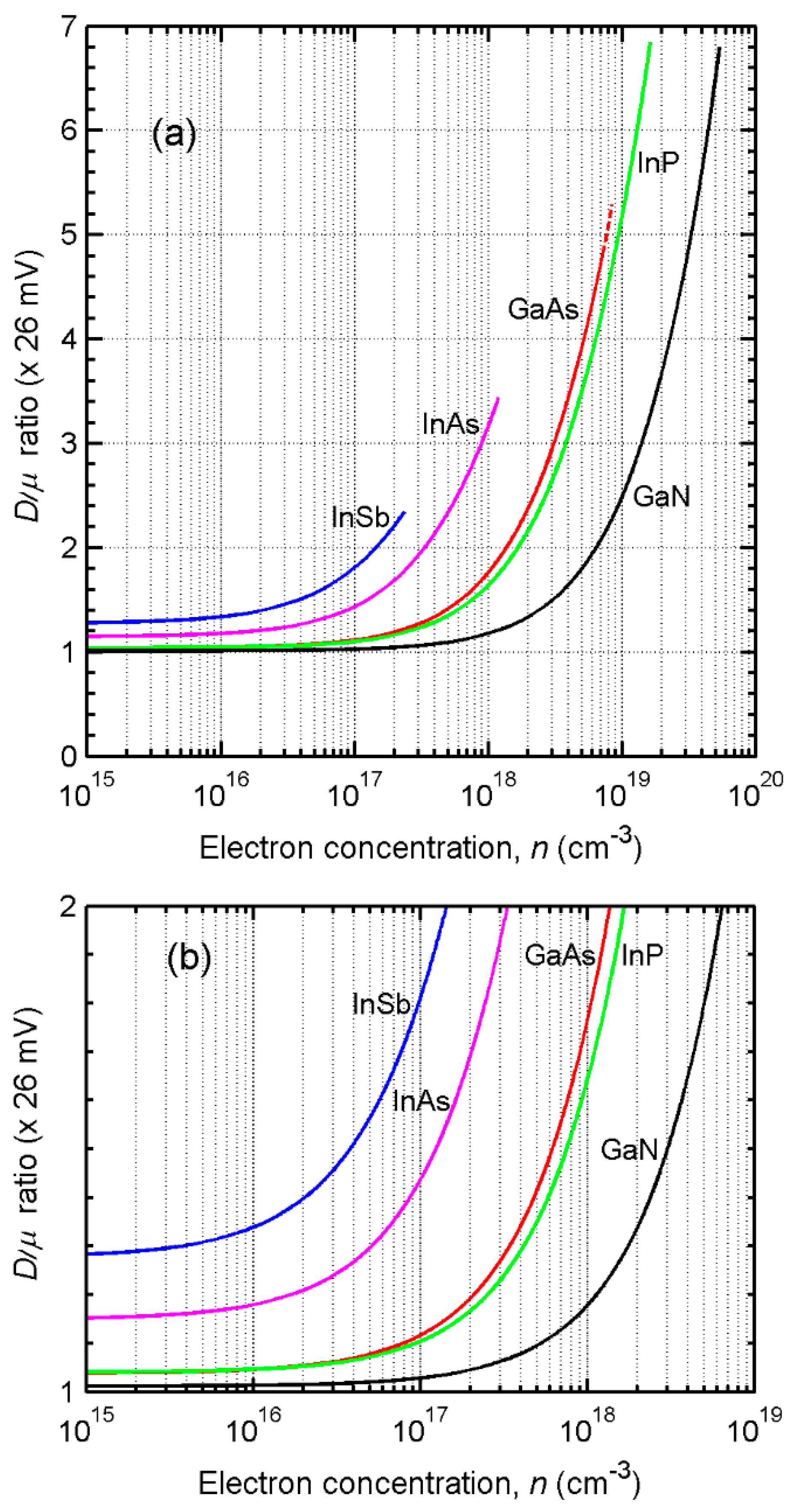
Figure 6 shows the difference in values of the D/μ ratios due to band nonparabolicity for the conduction electrons of the common compound semiconductors, as plotted as a function of the electron concentration. In the figure, the set of solid curves represents the D/μ ratios displayed in Figure 5, and the set of dashed curves represents the D/μ ratios calculated with the parabolic band approximation (β = 0) for the same temperature (TL = 300 K). For accurate comparison in the nondegenerate condition, an enlarged detailed plot is presented additionally in Figure 6b, where a horizontal dotted line is drawn to mark the value of the D/μ ratio at the crossover points. At TL = 300 K, it is D/μ = 45.7 mV.
From Figure 5 and Figure 6, the following is observed as compared to the values obtained by the parabolic band approximation. For GaN, which has a very small value of α (the present work used α = 0.19), due to the very wide bandgap of 3.44 eV [5,25], the nonparabolicity effect is very small and can be neglected (approximately 4% around n = 5 × 1019 cm−3). For GaAs and InP, which have relatively large bandgap energies of 1.42 eV and 1.35 eV, respectively [5,25], the effect is also small and can be neglected, causing an increase of only 4% in the nondegenerate condition (the case for GaAs is almost the same as that for InP). However, it is significantly large in heavy-doping conditions, and causes a decrease of approximately 10% around n = 1019 cm−3 for InP (for GaAs the effect is discussed separately later in this case). For InAs, which has a narrow bandgap of 0.35 eV [5,16,25], the effect is substantially large, increasing by 15% in the nondegenerate condition, and decreasing by approximately 18% around n = 1018 cm−3. The nonparabolicity effect is much more significant with InSb, which has a very narrow bandgap of about 0.2 eV [16,25,26]. For this semiconductor, it is worth noting that a maximum error caused by the parabolic band approximation occurs in the nondegenerate condition for the possible practical range of doping densities, and amounts to 28%.
Figure 4, Figure 5 and Figure 6 have been obtained by considering only the lowest CB. However, the compound semiconductors used for these figures have another upper CB, in which it is possible for some electrons to occupy at very large Fermi energies, i.e., in heavy-doping conditions. In GaAs, the upper CB is separated only by 0.3 eV from the lowest CB, while it is separated by 0.4 eV or more than this energy in the other semiconductors (∆Г−L = 0.3 eV for GaAs, ∆Г−X = 0.4 eV for InSb, ∆Г−L = 0.59 eV for InP, ∆Г−L = 0.72 eV for InAs, and ∆Г−X = 1.22 eV for GaN) [26]. It has been found at room temperature that for the semiconductors, except GaAs, the electron concentration in the upper CB is negligibly small at ηc = 10; this is not so for GaAs when ηc > 7 or n > 7.5 × 1018 cm−3, as indicated by the extension of the D/μ ratio curve for GaAs with dashes for values above D/μ = 4.8 (×26 mV) in Figure 5a.
In GaAs, the upper CB consists of four equivalent L-valleys. The electron concentration in this CB, nL, has been additionally calculated in thermal equilibrium for TL = 300 K, and the ratio of nL to nГ is plotted as a function of ηc in Figure 7 (nГ denotes the electron concentration in the lowest CB (Г-valley). For the calculation of nL, α = 0.46 for the nonparabolicity [19] and 0.56me, where me is the free electron rest mass, for the electron DOS effective mass [26] were used for the L-valleys, based on the isotropic band approximation. Figure 7 shows that at ηc = 10, the concentration ratio, nL/nГ, amounts to 0.16, and at ηc = 12, it reaches up to 0.63, due to a very large value of the effective DOS, Nc, of the upper CB, which is 24 times larger than that of the lowest CB. Therefore, for GaAs the electron population in the upper CB cannot be neglected and will affect the D/μ ratio for conduction electrons at very large Fermi energies or electron concentrations at room temperature. In addition, from Figure 7, the following very important fact can be deduced. If we assume that the energy separation (∆Г−L) of GaAs is 0.4 eV, rather than 0.3 eV, then the concentration ratio at ηc = 10 will decrease to less than 1%, which is the value corresponding to the concentration ratio when the position of ηc has changed from 10 to 6.1 in Figure 7. This suggests that in semiconductors, the electronic property of the band structure above 0.4 eV from the lowest CB edge does not affect the D/μ ratio for conduction electrons generally at room temperature, unless they are doped excessively so that ηc exceeds 10, even though they have multiple CB bands.
Since essentially the D/μ ratio, or the diffusion coefficient, for electrons represents the average property of a single electron for diffusion, the average D/μ ratio for the total conduction electrons in GaAs can be obtained by taking a weighted average using the electron concentrations of the lowest and upper CBs as follows:
Thus, it has been calculated and presented in Figure 8 as a function of the reduced FE in the plot (a) and also as a function of the total electron concentration, i.e., n = nГ + nL, in the plot (b). In this figure, the average D/μ ratio calculated in the case of β = 0 (for both the lowest and upper CBs) are additionally shown by a dashed curve for comparison. These two curves are also compared in the figure with the other additional curve obtained by considering the lowest CB only, i.e., completely neglecting the existence of the upper CB (n = nГ in this case). All of the results are for TL = 300 K.
Figure 8 shows that the error arising from completely neglecting the electron population of the upper CB increases notably for ηc > 7 or n > 7.4 × 1018 cm−3 (the concentration value corresponding to the average D/μ ratio when ηc = 7), and becomes dramatically large for ηc > 10 or n > 1.5 × 1019 cm−3 (the concentration value corresponding to the average D/μ ratio when ηc = 10). The most interesting and important feature observed from this figure is that the average D/μ ratio becomes saturated, with a maximum value D/μ = 6.1 (×26 mV), and then decreases. The saturation occurs at ηc = 10.2 or n = 1.6 × 1019 cm−3 (when nL/nГ = 0.17 from Figure 7). It should be noted that since the FE is at least 0.036 eV less than the bottom energy of the upper CB for ηc < 10.2 (the saturation point value) at TL = 300 K, the D/μ ratio for nL is approximately equal to its value given in the nondegenerate condition, i.e., 26 mV (=kBTL/q), for this range of ηc (refer to the case of ηc = −1.4 and β = 0.012, the value of β for the L-valleys at TL = 300 K, in Figure 2). This value of the D/μ ratio is in particular approximately seven times smaller than that of the D/μ ratio for nГ noted at ηc = 10.2, which amounts to 6.9 (×26 mV) in Figure 8a or Figure 8b. As a result, the increasing rate of the average per electron of the total kinetic pressure, or kinetic energy density, of electron gases in the CBs should be reduced continuously with increasing nL, resulting in the appearance of the saturation property. Note in Figure 8 that a similar saturation property also appears for the average D/μ ratio (β = 0) for the same reason, but the effect of nL on the saturation property is more severe in this case since the saturation is produced at a reduced maximum value of D/μ = 5.9 (×26 mV). The reason is that the concentration ratio nL/nГ increases more rapidly with increasing ηc when β = 0, which can be verified by observing that the saturation is caused by a smaller value of ηc in the plot (a) and also a smaller value of n in the plot (b).
It is shown in Figure 8b that due to the electron population in the upper CB, the band nonparabolicity effect for a given electron concentration is suppressed considerably so that it is only approximately 4% around n = 1019 cm−3, which can be well compared to the case of InP, i.e., approximately 10% around the same value of n, as noted previously. However, the effect is noted to be approximately 7% around n = 7 × 1018 cm−3, and becomes much larger for n > 1.2 × 1019 cm−3, at which the two average D/μ ratios are both equal in value in Figure 8b. It is very interesting to see in this plot that for n > 1.2 × 1019 cm−3, band nonparabolicity causes the average D/μ ratio to exceed the average D/μ ratio (β = 0) significantly, which is opposite to the general aspect of property 2 observed from Figure 3 for single CBs. The reason is, however, in principle the same as explained in connection with Figure 3, but the average kinetic energy of electrons in the case of β = 0 becomes smaller, contrary to property 2, for a given total electron concentration, n, in the two-CB system involved, because an increased FE result for β = 0 leads to a larger ratio of nL/nГ.
5. Conclusions
The currently used generalized Einstein relation for degenerate semiconductors with isotropic nonparabolic energy bands produces physically improper results, as well as losing numerical accuracy for large values of nonparabolicity parameters at room temperature. Therefore, a new generalized Einstein relation (a macroscopic equation and a formula) for degenerate semiconductors with isotropic nonparabolic energy bands was derived from the semiclassical momentum balance equation based on a drift–diffusion approximation by assuming a near-equilibrium transport condition. For the derivation, the novel concept of the effective temperature of a carrier gas has been introduced for the generalization of the classical kinetic theory for nonideal gases of carriers in semiconductors. The new generalized Einstein relation takes into account the carrier thermal energy diffusion effect completely, so that it can correctly reflect the effect of band nonparabolicity on the D/μ ratio for carriers in degenerate semiconductors with isotropic nonparabolic energy bands.
A theoretical analysis of the validity limit of the new Einstein relation for applied electric fields was also performed. The result indicates that it is generally valid for applied electric fields of the full linear regime for conduction electrons in semiconductors.
Many important nonparabolicity effects on the D/μ ratio for carriers in semiconductors were newly observed, and are summarized in the following. For any given FE, band nonparabolicity causes the D/μ ratio to always increase, and the nonparabolicity effect is largest in the nondegenerate condition. However, the effect is very different for a given electron concentration. In other words, band nonparabolicity causes the D/μ ratio to always increase in the nondegenerate condition, but it causes the D/μ ratio to always decrease in the high degenerate condition. Therefore, quite an interesting feature appears, such that for semiconductors with isotropic nonparabolic energy bands, when the electron concentrations are equal to the value of 2.33Nc, the D/μ ratios are always nearly equal to the value of 1.77kBTL/q, irrespective of the degree of nonparabolicity of their CBs.
The results calculated for common direct-bandgap compound semiconductors have additionally shown the following specific aspects for the nonparabolicity effect on the D/μ ratio for conduction electrons. For compound semiconductors that have a very wide direct bandgap, such as GaN, the nonparabolicity effect is negligibly small and can be disregarded. It is also negligibly small in the nondegenerate condition for direct-bandgap compound semiconductors, such as GaAs and InP, that have a relatively large bandgap energy. However, it can be significantly large in heavy-doping conditions in these semiconductors. This is another newly observed and critically important aspect. On the other hand, for compound semiconductors, such as InAs and InSb, that have a narrow direct bandgap, the nonparabolicity effect is substantially large in both the nondegenerate condition and the high degenerate condition. Therefore, the use of the parabolic band approximation for these semiconductors can give rise to considerable errors for the diffusion coefficients of electrons.
The dependency of the D/μ ratio and the FE on the electron concentration (or doping density in homogeneous materials) for a given semiconductor can be easily determined from the figures presented in the work. Therefore, they should be quite useful for semiconductor device design and material analysis. The generalized Einstein relation formulated in the present work can be utilized to more accurately analyze various depletion phenomena in semiconductor devices and materials in thermal equilibrium or near-equilibrium conditions, and also minority carrier diffusion properties in low-field or charge-neutral active regions of semiconductor devices, typically such as p-n diodes and bipolar transistors.
Acknowledgments
This work was supported by the Incheon National University Research Grant in 2014.
Conflicts of Interest
The author declares no conflict of interest.
Appendix A
The kinetic energy density tensor Q included in Equation (22) can be decomposed into physically meaningful parts by the following successive vector deduction and addition process:
where ko is such that .
Since ,
and
where
The result is:
In a special case where a constant, v is equal to vo by the relations and , and Q is simplified to:
which is the expression obtained for parabolic energy bands (α = 0).
References
- Peskir, G. On the diffusion coefficient: The Einstein relation and beyond. Stoch. Model. 2003, 19, 383–405. [Google Scholar] [CrossRef]
- Melehy, M.A. Diffusion-mobility generalized relationship and average kinetic energy of electrons in solid crystals. Proc. IEEE 1965, 53, 536. [Google Scholar] [CrossRef]
- Lindholm, F.A.; Ayers, R.W. Generalized Einstein relation for degenerate semiconductors. Proc. IEEE 1968, 56, 371–372. [Google Scholar] [CrossRef]
- Li, S.S.; Lindholm, F.A. Alternative formulation of generalized Einstein relation for degenerate semiconductors. Proc. IEEE 1968, 56, 1256–1257. [Google Scholar]
- Tiwari, S. Compound Semiconductor Device Physics, 1st ed.; Academic Press: San Diego, CA, USA, 1992; pp. 76–78. [Google Scholar]
- Nguyen, T.H.; O’Leary, S.K. Einstein relation for disordered semiconductors: A dimensionless analysis. J. Appl. Phys. 2005, 98, 076102. [Google Scholar] [CrossRef]
- Pierret, R.F. Advanced semiconductor fundamentals. In Modular Series on Solid State Devices, 1st ed.; Pierret, R.F., Neudeck, G.W., Eds.; Addison-Wesley Publishing: Reading, PA, USA, 1989; Volume 6, pp. 207–210. [Google Scholar]
- Copuroglu, E.; Mehmetoglu, T. Full analytical evaluation of the Einstein relation for disordered semiconductors. IEEE Trans. Electron Devices 2015, 62, 1580–1583. [Google Scholar] [CrossRef]
- McKelvey, J.P. Solid State and Semiconductor Physics, 1st ed.; Harper and Row: New York, NY, USA, 1966; pp. 134–156. [Google Scholar]
- Seeger, K. Semiconductor physics—An introduction. In Solid-State Sciences, 4th ed.; Cardona, M., Queisser, H.-J., Eds.; Springer: New York, NY, USA, 1989; Volume 40, pp. 10–17. [Google Scholar]
- Kane, E.O. Band structure of indium antimonide. J. Phys. Chem. Solids 1957, 1, 249–261. [Google Scholar] [CrossRef]
- Chakravati, A.N.; Nag, B.R. Generalized Einstein relation for degenerate semiconductors having non-parabolic energy bands. Int. J. Electron. 1974, 37, 281–284. [Google Scholar] [CrossRef]
- Azoff, E.M. Semiclassical high-field transport equations for nonparabolic heterostructure degenerate semiconductors. J. Appl. Phys. 1988, 64, 2439–2446. [Google Scholar] [CrossRef]
- Mukherjee, S.; De, D.; Mukherjee, D.J.; Bhattacharya, S.; Sinha, A.; Ghatak, K.P. Influence of light on the Einstein relation in III–V, ternary and quaternary materials: Simplified theory and a suggestion for experimental determination. Physica B 2007, 393, 347–362. [Google Scholar] [CrossRef]
- Ghatak, K.P.; Bhattacharya, S.; Bhowmik, S.; Benedictus, R.; Choudhury, S. The Einstein relation in quantum wires of III–V, ternary, and quaternary materials in the presence of light waves: Simplified theory, relative comparison, and suggestion for experimental determination. J. Appl. Phys. 2008, 103, 094314. [Google Scholar] [CrossRef]
- Lundstrom, M. Fundamentals of Carrier Transport, 2nd ed.; Cambridge University Press: Cambridge, UK, 2000; pp. 12–30, 151–153. [Google Scholar]
- Stewart, R.A.; Churchill, J.N. A fully nonparabolic hydrodynamic model for describing hot electron transport in GaAs. Solid-State Electron. 1990, 33, 819–829. [Google Scholar] [CrossRef]
- Bløtekjær, K. Transport equations for electrons in two-valley semiconductors. IEEE Trans. Electron Devices 1970, 17, 38–47. [Google Scholar] [CrossRef]
- Anile, A.M.; Romano, V. Nonparabolic band transport in semiconductors: Closure of the moment equations. Contin. Mech. Thermodyn. 1999, 11, 307–325. [Google Scholar] [CrossRef]
- Ye, L.; Stewart, R.A.; Churchill, J.N. On the effective mass in modeling nonstationary transport. J. Appl. Phys. 1987, 61, 2077–2079. [Google Scholar] [CrossRef]
- Koroleva, O.N.; Mazhukin, A.V.; Mazhukin, V.I.; Breslavskiy, P.V. Approximation of Fermi-Dirac integrals of different orders used to determine the thermal properties of metals and semiconductors. Math. Montisnigri 2016, 35, 37–53. [Google Scholar]
- Feng, Y.-K.; Hintz, A. Simulation of submicrometer GaAs MESFET’s using a full dynamic transport model. IEEE Trans. Electron Devices 1988, 35, 1419–1431. [Google Scholar] [CrossRef]
- Malorony, T.J.; Frey, J. Transient and steady-state electron transport properties of GaAs and InP. J. Appl. Phys. 1977, 48, 781–787. [Google Scholar]
- Shur, M. Physics of semiconductor devices. In Solid State Physical Electronics, 1st ed.; Holonyak, N., Jr., Ed.; Prentice-Hall International: London, UK, 1990; pp. 26–42. [Google Scholar]
- Singh, J. Physics of semiconductors and their heterostructures. In Electronics and VLSI Circuits, 1st ed.; Stephen, W., Ed.; McGraw-Hill: New York, NY, USA, 1996. [Google Scholar]
- Vurgaftman, I.; Meyer, J.R.; Ram-Mohan, L.R. Band parameters for III–V compound semiconductors and their alloys. J. Appl. Phys. 2001, 89, 5815–5875. [Google Scholar] [CrossRef]
Figure 1.
Approximation errors in percentage vs. the reduced Fermi energy (FE) ηc as calculated for various values of β. The solid curves display the errors induced by the empirical approximation, and the dashed curves for β = 0.12 and 0.18 by the binomial approximation.
Figure 1.
Approximation errors in percentage vs. the reduced Fermi energy (FE) ηc as calculated for various values of β. The solid curves display the errors induced by the empirical approximation, and the dashed curves for β = 0.12 and 0.18 by the binomial approximation.

Figure 2.
Calculated values of the D/μ ratios for electrons as a function of the reduced FE for selected various values of β. The dashed curve 1 displays the D/μ ratio calculated for electrons with the existing formula, Equation (6), for β = 0.06, and the dashed curve 2 for β = 0.18.
Figure 2.
Calculated values of the D/μ ratios for electrons as a function of the reduced FE for selected various values of β. The dashed curve 1 displays the D/μ ratio calculated for electrons with the existing formula, Equation (6), for β = 0.06, and the dashed curve 2 for β = 0.18.

Figure 3.
The same as in Figure 2, but as a function of the electron concentration normalized to the effective density of states (DOS), Nc. The dashed curve 1 displays the D/μ ratio calculated with the existing formula, Equation (6), for β = 0.18.
Figure 3.
The same as in Figure 2, but as a function of the electron concentration normalized to the effective density of states (DOS), Nc. The dashed curve 1 displays the D/μ ratio calculated with the existing formula, Equation (6), for β = 0.18.

Figure 4.
Calculated values of the D/μ ratios for conduction electrons as a function of the reduced FE for common direct-bandgap compound semiconductors at TL = 300 K. The plot (a) is for ηc < 3; and the plot (b) for ηc > 3.
Figure 4.
Calculated values of the D/μ ratios for conduction electrons as a function of the reduced FE for common direct-bandgap compound semiconductors at TL = 300 K. The plot (a) is for ηc < 3; and the plot (b) for ηc > 3.

Figure 5.
The same as in Figure 4, but as a function of the electron concentration. The plot (b) is an enlarged detailed view of the plot (a) for the values in the nondegenerate condition.
Figure 5.
The same as in Figure 4, but as a function of the electron concentration. The plot (b) is an enlarged detailed view of the plot (a) for the values in the nondegenerate condition.

Figure 6.
The values of the D/μ ratios (solid curves), shown in Figure 5, are compared with those of the D/μ ratios (dashed curves) calculated with the parabolic band approximation (β = 0) for the same temperature. The plot (b) is an enlarged detailed view of the plot (a) for the values in the nondegenerate condition.

Figure 7.
Calculated electron concentration ratio of nL to nГ as a function of the reduced FE for GaAs in thermal equilibrium (TL = 300 K).
Figure 7.
Calculated electron concentration ratio of nL to nГ as a function of the reduced FE for GaAs in thermal equilibrium (TL = 300 K).
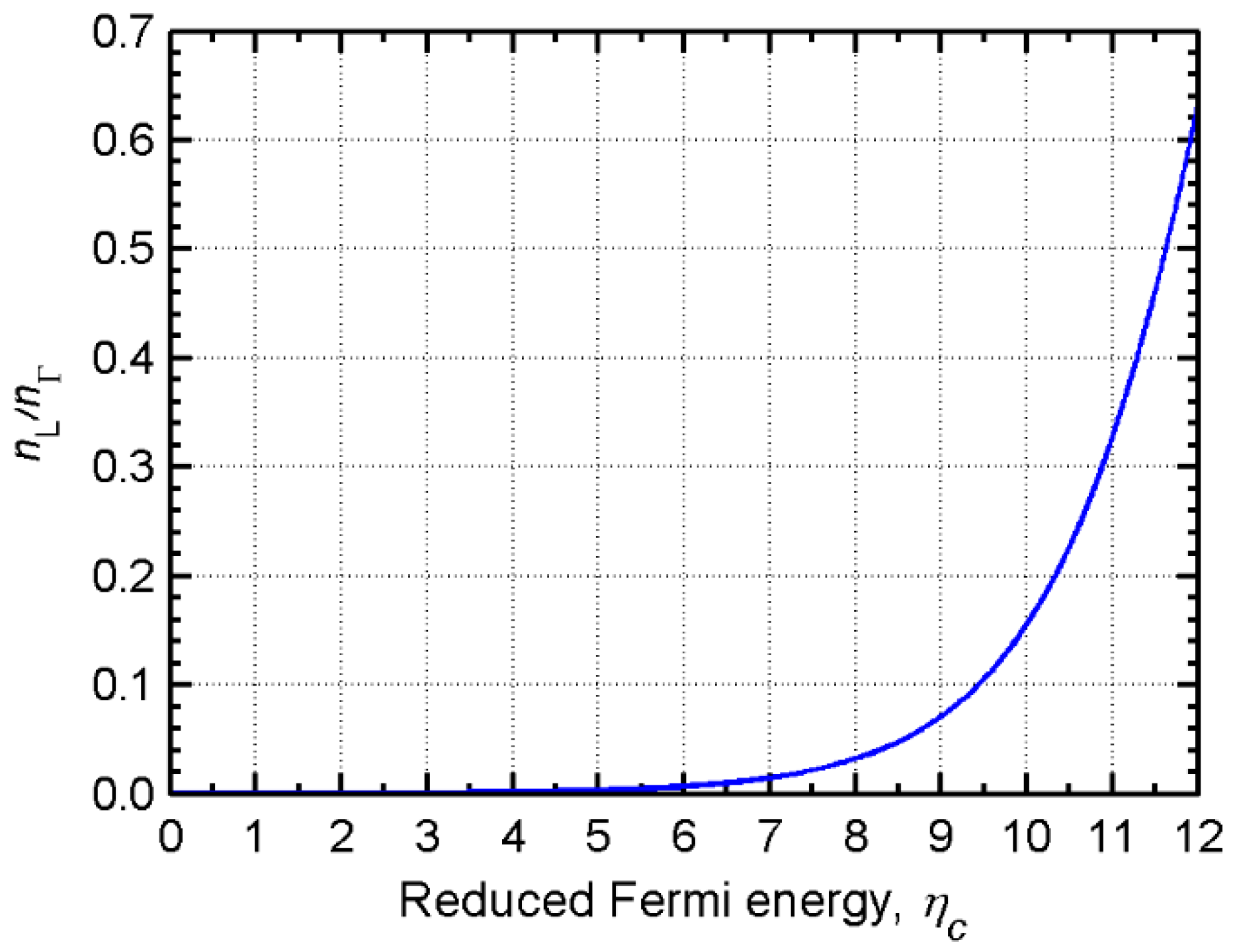
Figure 8.
Calculated values of the D/μ ratios for conduction electrons as a function of the reduced FE in (a); as well as a function of the electron concentration in (b), in the three different cases for GaAs (TL = 300 K).
Figure 8.
Calculated values of the D/μ ratios for conduction electrons as a function of the reduced FE in (a); as well as a function of the electron concentration in (b), in the three different cases for GaAs (TL = 300 K).

Table 1.
Material parameter values used for the calculation of the D/μ ratios for conduction electrons at TL = 300 K.
Table 1.
Material parameter values used for the calculation of the D/μ ratios for conduction electrons at TL = 300 K.
| InSb | InAs | InP | GaAs | GaN | |
|---|---|---|---|---|---|
| α | 5.72 eV−1 | 2.73 eV−1 | 0.67 eV−1 | 0.64 eV−1 | 0.19 eV−1 |
| β | 0.1479 | 0.0706 | 0.0173 | 0.0165 | 0.0049 |
| mc | 0.0135me | 0.025me | 0.077me | 0.067me | 0.19me |
| Nc | 3.936 × 1016 cm−3 | 9.919 × 1016 cm−3 | 5.31 × 1017 cm−3 | 4.352 × 1017 cm−3 | 2.078 × 1018 cm−3 |
© 2017 by the author. Licensee MDPI, Basel, Switzerland. This article is an open access article distributed under the terms and conditions of the Creative Commons Attribution (CC BY) license (http://creativecommons.org/licenses/by/4.0/).
Share and Cite
MDPI and ACS Style
Jyegal, J. Thermal Energy Diffusion Incorporating Generalized Einstein Relation for Degenerate Semiconductors. Appl. Sci. 2017, 7, 773. https://doi.org/10.3390/app7080773
AMA Style
Jyegal J. Thermal Energy Diffusion Incorporating Generalized Einstein Relation for Degenerate Semiconductors. Applied Sciences. 2017; 7(8):773. https://doi.org/10.3390/app7080773
Chicago/Turabian StyleJyegal, Jang. 2017. "Thermal Energy Diffusion Incorporating Generalized Einstein Relation for Degenerate Semiconductors" Applied Sciences 7, no. 8: 773. https://doi.org/10.3390/app7080773
Note that from the first issue of 2016, this journal uses article numbers instead of page numbers. See further details here.