
Widely-Tunable Ring-Resonator Semiconductor Lasers
by

Tin Komljenovic
1,*, 
Linjun Liang
2,
Rui-Lin Chao
3,
Jared Hulme
4,
Sudharsanan Srinivasan
5,
Michael Davenport
1 and
John E. Bowers
1
1
Electrical & Computer Engineering, University of California Santa Barbara, Santa Barbara, CA 93106, USA
2
Institute of Lightwave Technology, Beijing Jiaotong University, Beijing 100044, China
3
Department of Electrical Engineering, National Central University, Taoyuan 451700, Taiwan
4
Hewlett Packard Labs, 1501 Page Mill Rd, Palo Alto, CA 94304, USA
5
Juniper Networks, Inc., 1133 Innovation Way, Sunnyvale, CA 94089, USA
*
Author to whom correspondence should be addressed.
Appl. Sci. 2017, 7(7), 732; https://doi.org/10.3390/app7070732
Submission received: 27 June 2017
/
Revised: 7 July 2017
/
Accepted: 12 July 2017
/
Published: 17 July 2017
(This article belongs to the Section Optics and Lasers)
Abstract
:Chip-scale widely-tunable lasers are important for both communication and sensing applications. They have a number of advantages, such as size, weight, and cost compared to mechanically tuned counterparts. Furthermore, they allow for integration in more complex integrated photonic chips to realize added functionality. Here we give an extensive overview of such lasers realized by utilizing ring resonators inside the laser cavity. Use of ring resonators for tuning allows for wide-tunability by exploiting the Vernier effect, and at the same time improves the laser linewidth, as effective cavity length is increased at ring resonance. In this review, we briefly introduce basic concepts of laser tuning using ring resonators. Then, we study a number of laser cavity configurations that utilize two ring resonators, and compare their tuning performance. We introduce a third ring resonator to the laser cavity, study three different cavity configurations utilizing three ring resonators, and select the optimal one, for which we show that laser tuning is straightforward, provided there are monitor photodetectors on-chip. Finally, we give a literature overview showing superior linewidth performance of ring-based widely-tunable lasers.

1. Introduction
Chip-scale widely-tunable lasers have been of interest for some time [1]. Applications range from communications, especially wavelength-division multiplexing systems (WDM), to a number of sensing applications, such as wavelength-steered light detection and ranging (LIDAR)for autonomous driving [2]. There are also numerous other sensor applications that rely upon the ability to sweep the laser frequency over a wide wavelength range, such as spectroscopy or backscatter reflectometers.
A fully-integrated widely-tunable semiconductor laser has a number of advantages compared to the mechanically tuned counterparts—size, weight and cost are most obvious ones, but equally important, is the ability to integrate them with other components to provide added functionality on the same chip. Integration using monolithic or heterogeneous processes assembles many devices or optical functionalities on a single chip, so that all optical connections are on-chip and require no external alignment. The need for external alignment can become a bottleneck at large enough volumes, and result in increased cost.
Photonic integrated circuits (PIC) can be realized in a number of platforms, but for efficient on-chip light generation, a direct bandgap semiconductor is needed. Historically, the first integrated photonic circuits with lasers were realized on gallium arsenide (GaAs) or indium phosphide (InP) substrates for the same reason [3]. The performance of lasers on native III-V substrate is considered state-of-the-art, but the cost due to the lower size of wafers, and higher cost of substrates, still presents a barrier to some markets. More recently, optical components are being integrated on silicon (Si) substrates for fabricating large-scale photonic integrated circuits that co-exist with micro-electronic chips. Additionally, the economy of scale in the microelectronics industry offers much a larger size (300 mm) and lower cost wafers, which consequently offers cheaper cost per unit die area, provided the volumes are high enough to offset higher initial investment [4]. Furthermore, the maturity of Si processing is vastly superior as shown with the latest generation of microprocessors having more than a few billion transistors densely packed in an area of ~450 mm2. This is many orders of magnitude more complex than the most advanced InP PICs. As the complexity of PICs increase, yield can be a limiting factor, and that is one more reason why the Si platform is actively being pursued for complex PICs. In the past 15 years, a whole range of photonic components, including filters, (de) multiplexers, splitters, modulators, and photodetectors, have been demonstrated, mostly in the silicon-on-insulator (SOI) platform [5]. The SOI platform is especially suited for standard communication bands at 1300 nm and 1550 nm, as silicon (n = 3.48) and its oxide SiO2 (n = 1.44) are both transparent, and form high-index contrast, high-confinement waveguides ideally suited for medium to high-integration PICs. In the shorter term, the rationale of silicon photonics is a reduction of the cost of photonic systems, most probably the ones targeted to the large volume data center market, but in the longer term, photonics should help solve the communications bottleneck, with the introduction of optics inside a high-performance electronic chip [6].
However, electrically pumped efficient sources on silicon remain a challenge due to the indirect bandgap of silicon. There have been some demonstrations with, e.g., strained Ge [7], but the performance of such sources is still very far from practical products. A large number of current Si photonic PICs use hybrid approaches in which Si PIC is coupled to III/V PIC that provides gain and lasing. Such an approach requires precise alignment, and arguably has scaling limitations.
An alternative approach, most commonly called heterogeneous integration, bonds pieces of III/V materials on patterned Si wafer and then processes them using the same lithography tools. The advantage of this approach is that the alignment tolerances are significantly reduced, as devices are defined using lithography alignment marks after bonding of larger III/V pieces. Such an approach is currently widely used by both academia (e.g., University of California Santa Barbara (UCSB) [5,8], Ghent University [9,10]) and industry (Intel [11], Juniper Networks (formerly Aurrion) [12], Hewlett Packard Enterprise (HPE) [13]). This approach still has a theoretical disadvantage, as it uses expensive III/V wafers, and there is a size mismatch between typical Si wafers (12’’), and typical III/V wafers (3’’). Due to this reason, direct growth of III/V on silicon is currently being actively researched, with some very impressive demonstrations [14,15]. Direct growth has a potential to further reduce cost, but currently still has problems with lifetimes of the devices, despite using quantum dots, that are significantly more resilient to defects and dislocation impairments, than quantum wells. Direct growth, although a topic of great current interest, lies outside the scope of this manuscript. All the devices demonstrated in this manuscript use III/V quantum wells bonded to patterned SOI wafers. This approach gives the best of both worlds: high-gain from optimized III/V materials, and superior passive and waveguide technology of the SOI platform.
The paper is organized as follows. In Section 2, we introduce basic concepts of laser tuning utilizing Vernier effect and ring resonators, and provide theoretical considerations on the influence of ring resonators to laser linewidth and other key parameters. In Section 3, we compare tuning and linewidth performance of a number of laser structures that utilize two different ring lengths for achieving wide tunability. In Section 4, we introduce methods to further improve the linewidth: use of an on-chip external cavity, and use of an on-chip high-Q resonator. We study their placement, and performance influence, and select a high-Q ring internal to the laser cavity as the optimal design. We then demonstrate that tuning of lasers with three rings of different circumference is straightforward, provided the PIC has on-chip monitor photodetectors. Lastly, we give a brief overview of widely-tunable lasers in literature in Section 5, and give conclusions in Section 6.
2. Basic Principle of Wide-Tunability Utilizing Ring Resonators
Wide-tunability in chip-scale semiconductor lasers is commonly achieved by utilizing the Vernier effect. The effect has been utilized both with sampled Bragg grating reflectors and ring resonators. Ring resonators, provided that the utilized waveguide platform offers sufficiently low propagation losses, have an advantage, as the effective cavity length at ring resonance is significantly enhanced, directly reducing linewidth [16,17].
A single ring resonator in add-drop configuration placed inside the laser Fabry-Perot cavity can be used for selecting an individual longitudinal mode. A typical transmission curve of a single ring resonator is shown in Figure 1a. An ideal ring with ideal broadband couplers (no wavelength dependence on the coupling strength) has a periodic response separated by ring free-spectral range (FSR), corresponding to the inverse round-trip time inside the ring.
where c is the speed of light in a vacuum, L is the circumference of the ring, and ng is the group refractive index. To guarantee single longitudinal mode operation, the FSR of the ring should be larger than the gain bandwidth of the laser. With typical gain bandwidths in the 60 nm range, corresponding to ~7.5 THz around 1550 nm, ring circumferences, assuming ng = 3, are limited to very small values, around 10 µm. Such small circumferences might be impractical for at least two reasons, despite SOI technology providing very sharp bend radii with low loss. Tight bends, with losses lower than 0.09 dB per bend for bending radiuses of only 1 μm, were demonstrated more than ten years ago [18]. The first problem is designing such short couplers (two are needed for add-drop ring configuration), and the second problem is providing wide wavelength tuning. In Si photonics, two tuning mechanisms are typically used: carrier based (either injection or depletion), or thermal based. Carrier injection results in increased losses due to free carrier absorption, while carrier depletion generally has much lower efficiency, but allows for higher speed, and is the method of choice for high-speed modulators. Thermal tuning is often used for slower adjustments (10s of kHz, limited by thermal constants of the whole structure), especially as with proper design, there is no change in optical losses with tuning. This is the main reason we use thermal heaters for all of our devices, as low losses allow for narrower linewidth. In this work, the heaters are deposited above Si waveguides, with ~1 µm of SiO2 deposited in-between, to prevent the interaction between the metal and the optical mode, which would result in increased propagation loss. Devices based on silicon are readily thermally tunable due to the large thermo-optic coefficient (dn/dT) of silicon. A value of dn/dT of 1.87 × 10⁻⁴/K at room temperature and 1.5 μm is generally reported, and the coefficient increases at shorter wavelength, to 1.94 × 10⁻⁴/K at 1.3 μm [19]. This translates to tuning of ~0.08 nm/°C at 1550 nm, so a temperature change for 60 nm of tuning can be as high as 700 °C. In practice, for passive devices, tuning ranges of up to 20 nm have been demonstrated [20], but still, such high temperatures close to the gain section would have negative influence on the laser performance.
FSR [Hz] = c/(L·ng),
Much more efficient tuning is possible by using two or more rings with slightly different circumferences. Typical circumferences of the two rings are designed so that the FSR is between 200 GHz and 400 GHz, corresponding to ~1.6 nm or ~3.2 nm in wavelength. This allows for tuning the ring in full FSR by changing the temperature by only 20–40 °C, which is straightforward to achieve. Due to the slight difference in circumference of the two rings, their resonances are mostly not aligned, and allow for single-mode operation in a much wider bandwidth that the FSR of an individual ring, as shown in Figure 1b. It is common to define tuning enhancement parameter M:
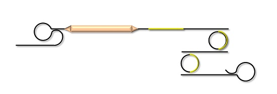
where L1 and L2 are the circumferences of Ring 1 and Ring 2, as shown in Figure 1b. The FSR of the combined two ring structure utilizing the Vernier effect then equals FSR1·M, where FSR1 is the FSR of Ring 1. We call the two ring structure that utilizes the Vernier effect to select single longitudinal mode a single wavelength filter (SWF). A typical widely-tunable ring-resonator semiconductor laser architecture using the SWF placed inside the Fabry–Perot cavity, with a gain element and phase tuner to align the longitudinal mode to the resonance of the SWF, is shown in Figure 2. Fabry–Perot mirrors could be realized as cleaved facets, but that would limit the integration potential of such lasers, so we utilize Sagnac loop mirrors, in which two same-side outputs of a coupler (directional, MMI or any other kind) are connected together to form a loop. Such a structure acts as a mirror whose reflectivity can be controlled by the coupling strength; from theoretically 100% for a 50:50 coupler, all the way to very low values, which are important for higher output powers. The analysis of the complex laser cavity is simplified by using the effective mirror theory Reff [21]. In the case of the laser cavity shown in Figure 2, Reff is a complex wavelength dependent mirror reflectivity, that includes the passive phase section, both ring resonators, and one of the loop mirrors (R2 in the case of Figure 2).
M = L1/(L2 − L1),
The complex amplitude reflectivity formula is given by the following expressions:
where αp and βp are the waveguide electric field propagation loss, and the effective propagation constant in waveguides, respectively, r2 is the amplitude reflectivity of the back-side mirror, Lx is the circumference of the ring, and the subscript X takes values 1 and 2 for the two rings in the SWF section. A number of useful laser parameters, including effective cavity length, mode spacing, and the adiabatic chirp reduction factor, can be determined using reff [22]. The chirp reduction is given by factor F = 1 + A + B, and the Lorentzian linewidth (Δv0) is reduced by F2, where A and B are defined as
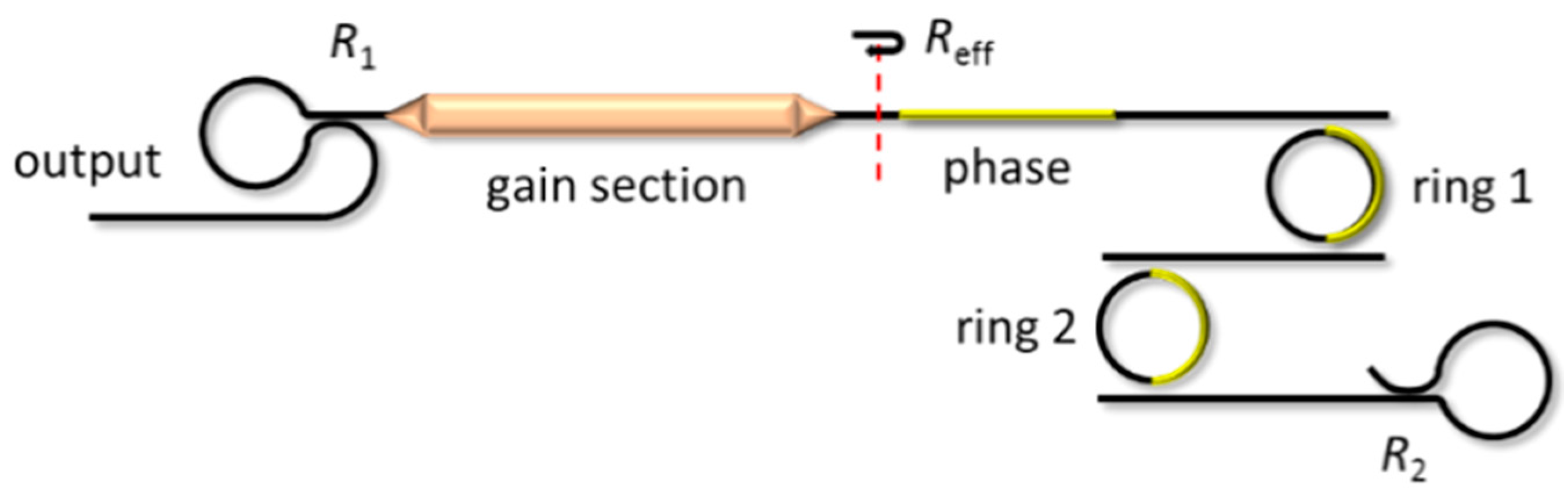
where αH is the linewidth enhancement factor, τin = 2neffLa/c is the roundtrip time in the active part of the cavity, where neff is the effective index of the gain section, and La is the length of the gain section. The A term, corresponding to the linewidth reduction from reduced longitudinal mode confinement, is often denoted as the ratio of the external (passive section) cavity path length to the gain section path length. As the effective length of a ring resonator is maximized at resonance, the A factor is maximized when the ring is placed exactly at resonance. The B term corresponds to the reduction in linewidth from the negative feedback effect, where a decrease in wavelength increases reflectivity (increasing photon density in the cavity), and hence decreases carrier density, which in turn causes the wavelength to increase, due to the carrier plasma effect. We plot some key parameters in Figure 3, where we assume a 3 mm long Fabry–Perot cavity and use identical SWF, as plotted in Figure 1b. The first takeaway from Figure 3 is that the effective cavity length increases at resonance, and it is well known that longer cavities generally correlate with lower linewidth. A longer “effective” cavity, at the same time, reduces the longitudinal mode spacing, so SWF has to be designed properly to provide sufficient passive side-mode suppression ratio (SMSR) for the laser to be single mode. The effective cavity length is actually a derivative of phase with respect to frequency, and, as expected, the phase changes faster around the resonance. Finally, we plot the A, B, and F factors in Figure 3d. As the B factor is antisymmetric around the resonance, and has a maximum when slightly detuned from the resonance, the result is that the total effect F is actually maximized off resonance. The phase section in the cavity can be used for a slight detuning of the laser oscillation with respect to the minimum cavity loss condition (resonator resonance) for best linewidth performance.
3. Comparison of Classical Widely-Tunable Architectures
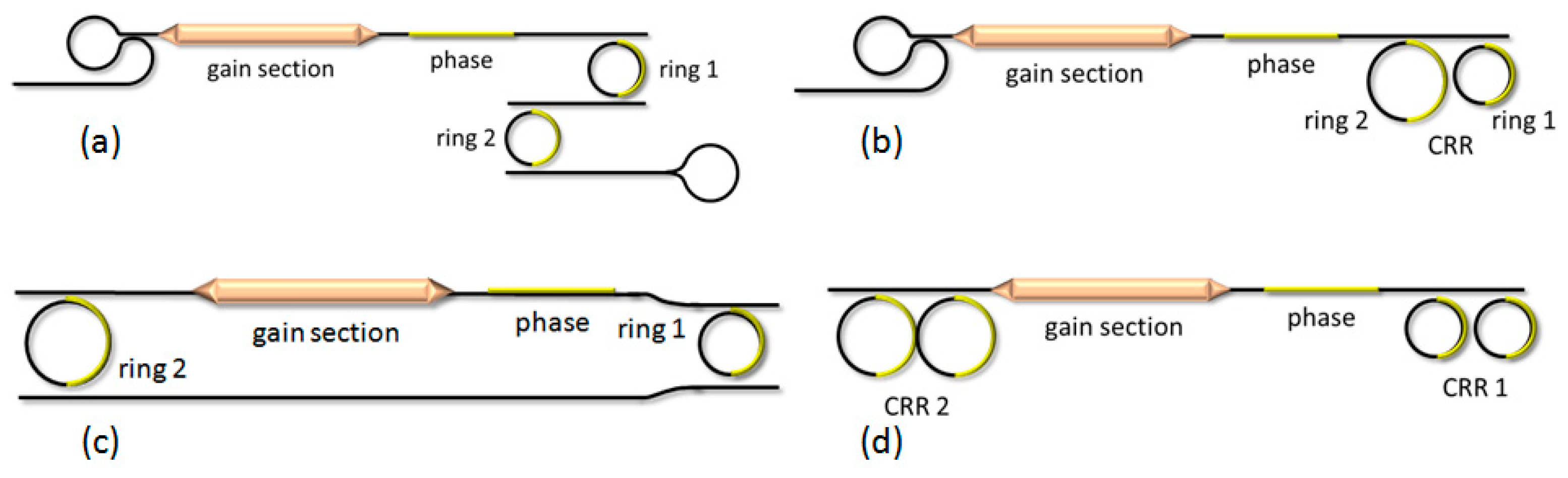
We compare four ring-based laser topologies, as shown in Figure 4, all of which have rings with two different circumferences to form the Vernier effect for tuning.
The first is a ring-bus-ring (RBR) laser, which utilizes two ring filters in series in add-drop configuration, and two Sagnac loop mirrors. The second is a single-sided coupled-ring resonator (CRR 1×) laser which utilizes a CRR mirror on one side as both reflector and filter, and a Sagnac loop mirror on the other side. The third is a Vernier racetrack laser, which utilizes two bus waveguides, one of which has a gain region and phase tuner, and two ring resonators that are coupled to the bus waveguides. The fourth design is a double-sided coupled-ring resonator (CRR 2×) laser, which utilizes a CRR mirror on both sides as both reflector and filter. All lasers have resistive heaters overlaying the rings to provide active tuning of the wavelength. Ring circumferences of the RBR laser are 256 μm and 271 μm, giving an expected tuning range of 42.1 nm, with the power coupling coefficient same for all couplers, and equal to 20%. For the CRR 1× laser, the selected circumference values for Ring 1 and Ring 2 were 337 μm and 368 μm, respectively, and the selected power coupling coefficient values for Κ1, Κ2 and Κ3 are 2.25%, 2.25% and 36%, respectively. This results in an expected tuning range of 20.4 nm. A more detailed description of CRR mirror properties is found in [23]. Vernier racetrack laser has two rings, with circumferences equal to 400 μm and 420 μm, with the power coupling coefficient same for all couplers, and equal to 20%. The design tuning range is equal to 31.6 nm. Finally, the CRR 2× laser has two pairs of rings, each pair having nominally the same radius of 368 μm and 402 μm. The coupling coefficient values for both pairs are equal and the same to those on CRR 1× laser. The design tuning range is 18.6 nm. The calculated function of the passive ring filters is shown in Figure 5.
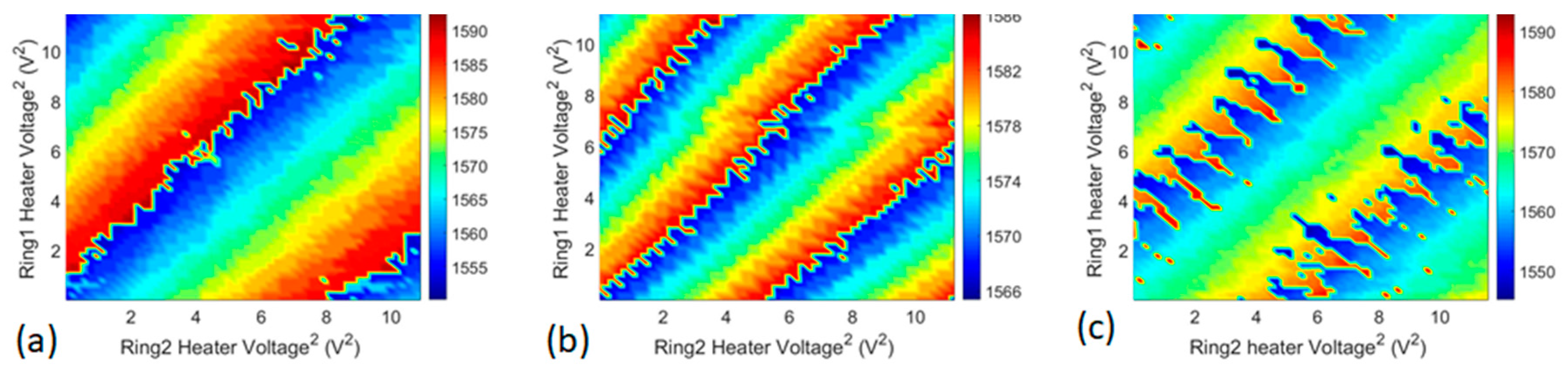
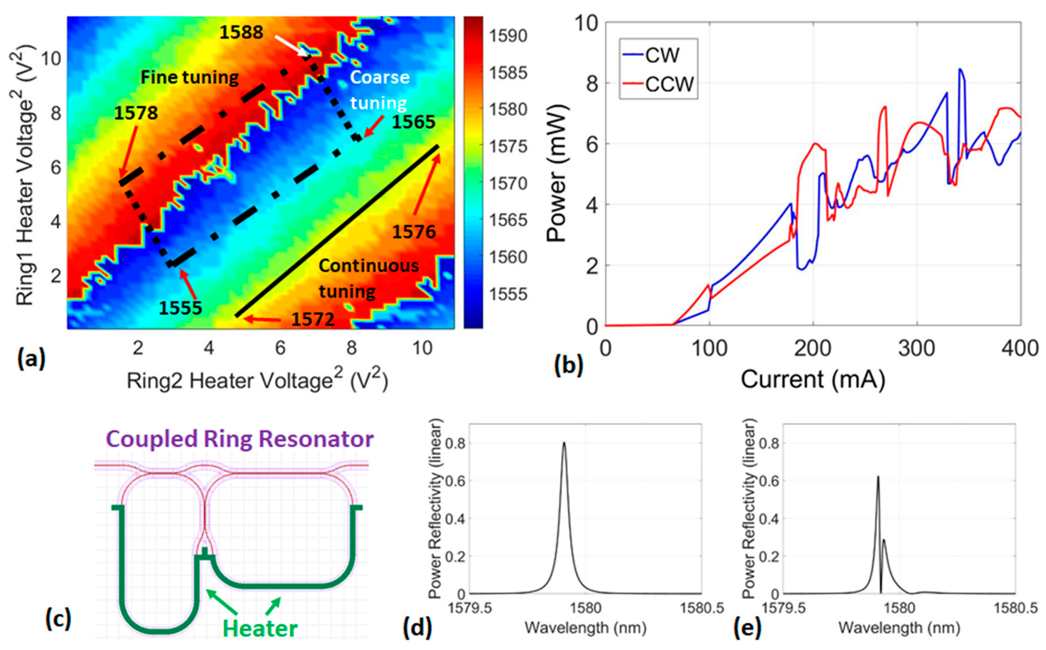
We have fabricated the lasers using heterogeneous III/V silicon process. Optical photographs of lasers are shown in Figure 6. Wavelength tuning for lasers was mapped out vs. ring heater voltage squared (proportional to power), as shown in Figure 7. The RBR laser had a measured tuning range of 42 nm, the CRR 1× laser had a measured tuning range of 21 nm, while the Vernier racetrack laser had a measured tuning range of 47 nm, and the theoretical tuning range of CRR 2× laser is 18.6 nm. We do not show the 2D tuning map for CRR 2× laser due to unpredictable tuning performance, that we addressed in Section 3.1. The tooth-shaped tuning map of the Vernier racetrack laser is due to the wavelength hopping between two wavelengths separated by the design tuning range of ~31 nm, when the laser work at the states where net gain between these two modes are similar in magnitude. The maximum measured double-sided output power was 7.7 mW for the RBR laser, 10.5 mW for the CRR 1× laser laser, 12.7 mW for the Vernier racetrack laser, and 14.2 mW for the CRR 2× laser. The output powers were measured using an integrating sphere.
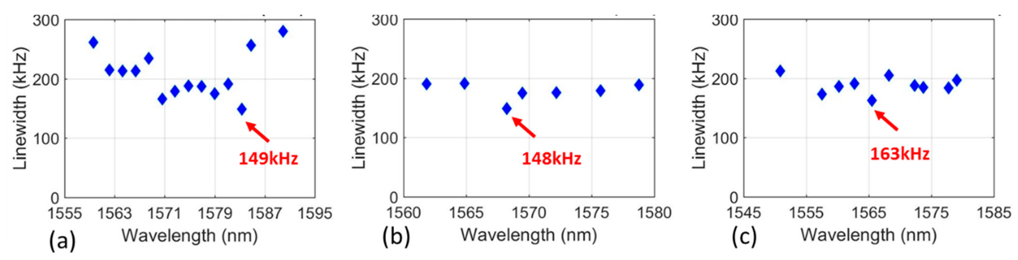
The laser linewidths were measured using the delayed self-heterodyne method, with 10 km of fiber in one arm, and an acousto-optic modulator with 100 MHz of frequency shift in the other arm. We quote the 3 dB Lorentzian linewidth calculated from −20 dB points. We show the measurements in Figure 8. All the measured configurations have linewidths in the 200 kHz range, with best results at 150 kHz. For the case of CRR 2× laser, in some certain lasing wavelengths, its measured linewidth can be as narrow as 196 kHz, however, the stable single-mode lasing performance cannot be sustained across the whole theoretical tuning range.
3.1. Discussion and Conclusions
Having analyzed, fabricated, and measured four different laser architectures, we conclude that the best design to realize a widely-tunable ring-resonator based laser is the RBR. The RBR laser has very predictable tuning, stable lasing due to the standing-wave nature of the resonator, and high passive side-mode suppression ratio (SMSR), resulting in high lasing SMSR. Added benefits are largely fixed mirror reflectivities due to the broadband Sagnac loop mirrors used. The biggest disadvantage of this architecture is a somewhat lower output power, although that can be corrected by placing a booster semiconductor optical amplifier (BSOA) after the laser. In a heterogeneously integrated design, integration of a BSOA is straightforward. The reason for lower output power is the tuning section, where light goes through each ring twice, increasing the insertion loss of the structure, and consequently, the cavity loss, but at the same time, this results in improved filtering, and higher passive SMSR.
We show tuning of the RBR laser in more detail in Figure 9a, where directions of fine (dashed red line) and coarse (dotted blue line) tuning are drawn. The black line shows continuous tuning without mode hops, where phase section corrects for the cavity length, as wavelength is tuned. To guarantee sufficient phase shift, the phase tuning section has to be optimized, and in general, up to a few nanometers of continuous tuning is possible, in practice, before temperatures at phase and ring tuners become excessive, and added heat starts to influence the laser performance significantly.
The CRR 1× laser has higher output power than RBR, primarily due to lower losses at the CRR reflector, compared to RBR filter realization. The biggest problem with CRR is the lower passive SMSR, translating to smaller tuning ranges, and/or lower laser SMSR.
As it is very challenging to design a single CRR structure with high SMSR, a logical idea would be to replace the Sagnac loop mirrors on both sides of the cavity with CRR structures. This further reduces the cavity losses, as shown, with the highest output powers obtained with CRR 2× laser. The laser also features high passive SMSR, but the tuning is extremely challenging, for several reasons. First is that the laser now has four controls for tuning, as each ring inside the CRR has its own tuner, and the fifth control would be the phase to align the longitudinal mode. A way to simplify the control would be using a single heater shared per CRR structure. A problem with this approach is that the rings have to be exactly the same circumference to act as a reflector, and any non-symmetry or thermal crosstalk will lead to resonance splitting, as shown in Figure 9d,e. The problem is further complicated due to a need to have distinctly different coupling values between the two rings and the bus waveguide [23], which makes full symmetry impossible. For our laser, we have designed independent heaters for each ring, and have also provided the ability to use the two heaters as one big heater covering both rings for each CRR structure, but in all cases, the tuning was very challenging. Due to such complicated controls, it is hard to recommend the CRR 2× structure, despite it having the highest output power.
The last considered structure, Vernier racetrack laser, has high output power, is straightforward to control, and has decent SMSR, but as it has a ring type of cavity, it inherently has bidirectional lasing, where two travelling waves compete for gain. We show the clockwise (CW) and counterclockwise (CCW) output powers in Figure 9b, and as the bias current is changed, the output powers in two directions also change. The same can happen as the laser is tuned, or laser operating temperature changes.
4. Advanced Designs for Linewidth Reduction
Linewidths of Si ring based semiconductor lasers are typically in sub-MHz range (for comparison, see Section 5), compared with typical linewidths of III/V lasers that are in a few MHz range. Here we describe methods for improving linewidth even further. It should be noted that methods described here generally improve Lorentzian, or white-noise limited, linewidth. The 1/f contribution of the phase noise to laser linewidth depends on many parameters, including sources of technical noise, such as current supplies, etc. To improve long-term stability of a semiconductor laser, locking to stable high-Q resonators is typically employed. A demonstration of locking a ring based widely-tunable semiconductor laser to a high-Q resonator made in SiN has shown significant reduction of low-frequency noise [24], and such resonators can be integrated on the same chip [25]. Laser locking to the external resonator lies outside the scope of the paper, but shows potential for extremely stable chip-scale laser, especially as SiN has lower thermo-optic coefficient than Si.
4.1. Utilizing Delayed On-Chip Optical Feedback
A technique that has often been employed for improving the laser linewidth uses delayed optical feedback. Semiconductor lasers, as is well known, can significantly be affected by external optical feedback. For that reason, in the majority of applications, great care is taken to coat the laser facets with anti-reflection coating, and to place optical isolators as close to the cavity as possible; but as controlled feedback can improve certain laser parameters, it has been extensively studied. Depending on specific conditions, optical feedback has been shown to make the laser multi-stable, have hysteresis phenomena, enhance, prolong or suppress the relaxation oscillation in the transient output, improve the laser’s performance through noise suppression, reduce nonlinear distortion and modulation bandwidth enhancement, and, what is most relevant for our application, improve the laser linewidth [26,27,28,29,30,31].
The effects of feedback are typically divided into five distinct regimes with well-defined transitions [32]. The classic paper from 1980 has been revisited and expanded [33]. It is shown that the change of amplitude signal (ΔE) always accompanies that of frequency change (Δv), due to feedback. The dependence is sinusoidal for weak feedback (ΔE ≈ E0∙cos(2kL), 2kL being the optical phase associated with distance to external reflector), and becomes more complicated, leading to switching, hysteresis, and chaos, for higher levels of feedback. The full dynamics are complex and depend on many laser parameters, such as gain, loss, photon and carrier lifetime, and above all, the linewidth enhancement factor αH. The feedback behavior can further be separated into four distinct regions: short vs. long cavities, and coherent vs. incoherent feedback. The latter condition relates the external cavity length L to the coherence length Lcoh of the unperturbed source. The distinction between short and long cavities is made based on the relation between the relaxation resonance frequency (fR), and the external cavity frequency. For short cavities, the length L < c/(2fR) and the oscillation regime is dependent upon the phase of the external path length. For long cavities L > c/(2fR), no dependence of the oscillation regime on phase should be observed.
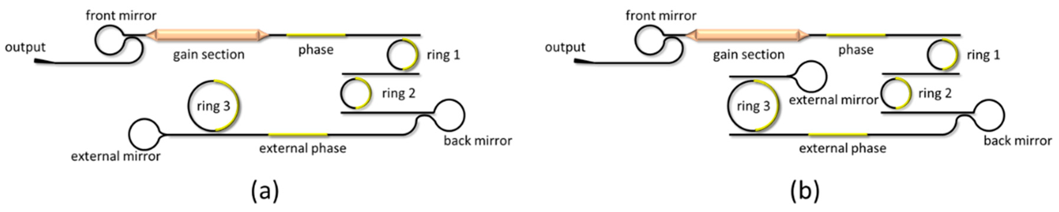
A schematic diagram of the integrated widely-tunable laser with on-chip external cavity is shown in Figure 10. The gain section is inside a 2 mm long cavity formed by loop-mirrors. The lasing wavelength is determined by the SWF formed from two ring resonators, and a cavity phase section, all of which are controlled by thermal phase tuners. The front loop mirror (at the output of the laser) has a 10% power reflection, and the output of the laser is terminated at the facet at an angle of 7°, to minimize reflections. The back loop mirror, after the wavelength tuning section, has a power reflection of 60%, which couples part of the light to the external cavity. In order to allow for a long external cavity, a low-loss waveguide platform is needed. Here, we utilize optimized silicon waveguides with a loss of 0.67 dB/cm. The external cavity is ~4 cm long and has its own phase adjustment section and gain section. The gain section in the external cavity is used to control the level of feedback. The external cavity is coupled on the side with the tuning section, so that the tuning rings filter out any spontaneously emitted light from the external semiconductor optical amplifier (SOA), improving the phase noise, and consequently, the linewidth performance. In the case of sufficient forward bias in the external SOA, the extended cavity can lase by itself. At the laser output, there is an on-chip monitor photodetector (MPD) that uses the same epitaxial material as the laser and the SOA. We have demonstrated 54+ nm of tuning range with high SMSR (>45 dB). Output power is around 10 mW, which can easily be increased by the use of a booster SOA.
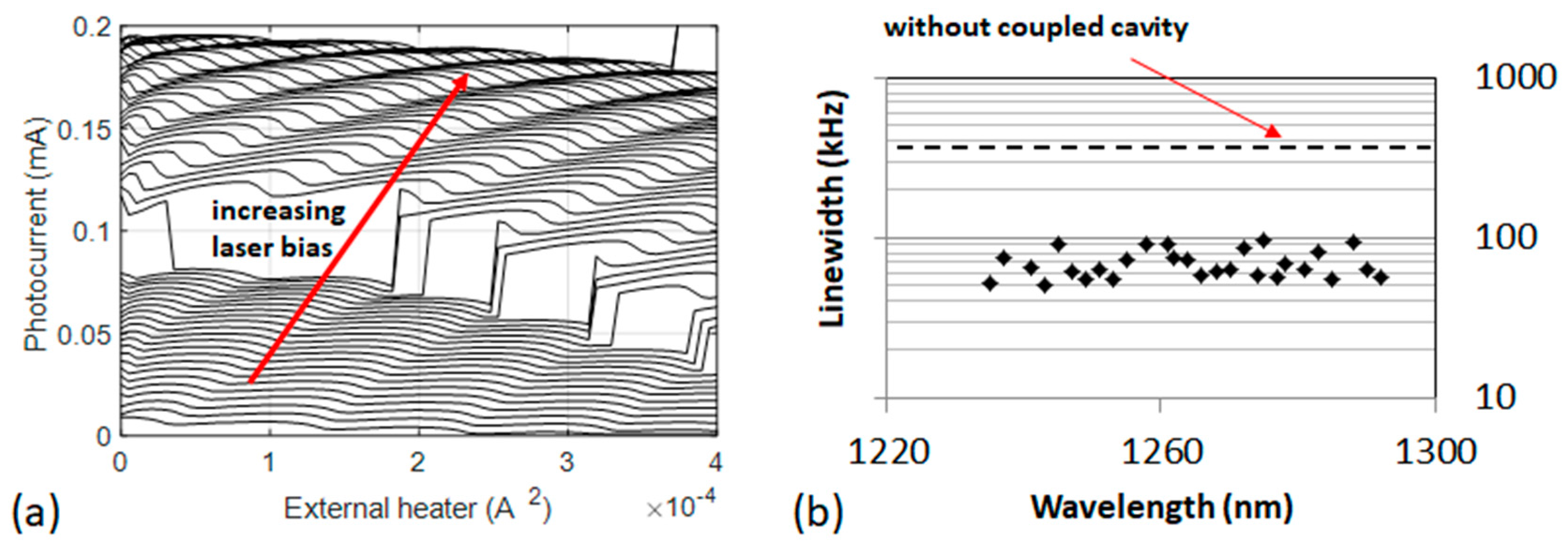
The on-chip MPD is a very useful tool to monitor the on-chip performance of a laser with an external cavity. It has been shown that lasers can be influenced by feedback levels as low as −90 dB [34], and a straightforward way to measure the feedback is to change the phase of the returned signal, while monitoring the laser output power. We show such a measurement in Figure 11a, where the external phase heater is tuned for various gain section biases, and output power is recorded by the on-chip MPD placed at the laser output. The resulting effect is an almost sinusoidal modulation of output power, with the phase of the returning signal as predicted for lower levels of feedback [33]. This signal can be used to phase align the two cavities, and improve the laser linewidth. We measured the linewidth of the laser with optimized feedback from the external cavity. The feedback was manually tuned for best performance, and results are shown in Figure 11b. The linewidths were below 100 kHz across the entire tuning range, and the best single-mode linewidth is 50 kHz. The quoted 3 dB linewidths are calculated from −20 dB points by assuming a Lorentzian lineshape using a delayed self-heterodyne method. Without the external cavity, the linewidths were in the 300 kHz range. It should be noted that the lasers were not packaged, so there were a number of sources of technical noise present.
We were able to measure even lower linewidths (below 20 kHz) at higher currents supplied to the external SOA, but the laser was multimode, with mode spacing determined by the external cavity length. In this case, both the relative intensity noise (RIN) and frequency noise spectrums have peaks at this mode separation. This shows that the external cavity can provide even better performance if the filtering section is optimized. We also believe that the external SOA increased the noise in the feedback signal, due to random spontaneous emission events, thus limiting the linewidth improvement performance over the theoretically predicted one, as for the measurements shown in Figure 11b, it was operated below transparency. Driving the external SOA more strongly would result in multimode behavior, as the SWF cannot filter out a single longitudinal mode of the external cavity in such a design. The Q of tuning rings is in the 10,000 range.
As an improvement of this work, we suggest use of a variable optical attenuator (VOA) in place of an SOA. VOAs could provide similar functionality in controlling the feedback level, with some differences. They only attenuate the signal, and so, depending on the configuration, potentially higher levels of feedback (regime V) would not be achieved, and the extinction ratio can be limited, at least for single stage structures. By cascading the VOAs, higher extinction ratios can be achieved, but with an increase in the insertion loss.
4.2. Utilizing On-Chip High-Q Resonator
High-Q resonators are another way of realizing narrow-linewidth lasers. We have explored the possibility of improving the linewidth of widely-tunable semiconductor lasers by utilizing an integrated high-Q ring cavity-on-chip [35]. Three potential strategies were analyzed: with the high-Q ring used as an external cavity with optical feedback in either all-pass or drop configuration, and with the high-Q ring being an integral part of the laser cavity.
The laser performance can be influenced by coupling the laser to a distanced single mirror, or to a high-Q cavity. For a laser coupled to a single mirror, two modes of operation can be identified, depending on if the external cavity free-spectral range is larger, or smaller, than the relaxation oscillation frequency (ωR) of the standalone laser [26]. For short cavities (external cavity FSR > ωR), the linewidth reduction is modest, but the feedback system has a very broad effective bandwidth able to suppress noise to frequencies much larger than ωR. In the case of a long cavity (external cavity FSR < ωR), the linewidth reduction can theoretically be much greater, but the effective bandwidth of the feedback system is narrower, resulting in strong external cavity modes. For stronger feedback, external cavity modes grow, and can cause the laser to become unstable. The optimal choice for narrow linewidth would therefore be an external cavity slightly shorter (FSR slightly larger) than ωR, with relatively strong feedback.
The limitation can be circumvented by coupling to a separate external cavity instead of a mirror. This has been typically done with Fabry–Perot cavities that were free-space coupled to semiconductor lasers [36,37]. The use of a separate cavity for feedback breaks the limitation, as one can engineer the cavity to have the FSR larger than ωR, keeping the laser stable with large effective bandwidth, and offering narrow linewidth due to increased photon lifetime inside the cavity. One of the benefits of integration is the reduced coupling loss between the laser and the external cavity.
For an integrated design, one can use a ring resonator as an external cavity, utilizing the low propagation loss provided by a silicon (or silicon nitride) waveguide. We have studied the two configurations shown in Figure 12 using the frequency chirp reduction approach, as outlined in Section 2, and by calculating the negative optical feedback responsivity and bandwidth, following the procedure outlined in [38]. Both external cavity configurations allow for high frequency chirp reduction factors. The external cavity in all-pass configuration, theoretically provides for narrowest linewidth, due to higher Q of the external resonator, as it has lower loading and also provides larger negative optical feedback bandwidth, but is the most sensitive to laser operating frequency, and also suffers from potential multimode behavior at higher external feedback levels, as the all-pass ring does not help with filtering out other longitudinal modes. The external cavity in add-drop configuration should be easier to operate single mode, due to added filtering of the add-drop resonator, but has narrower optical feedback bandwidth, as well as lower responsivity. Both configurations require proper alignment of multiple cavities, which can complicate the laser operation.
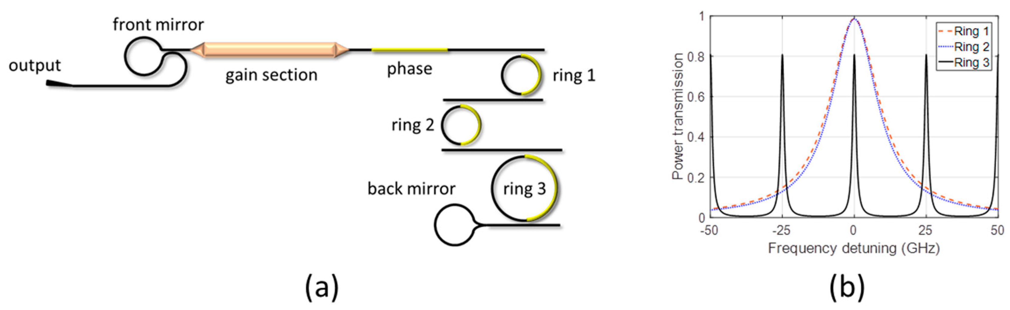
A third approach for using the high-Q resonator to improve laser linewidth is the inclusion of the high-Q resonator in a drop configuration as an integral part of the laser cavity, as shown in Figure 13a. The inclusion of a third ring resonator inside the cavity increases the cavity loss, and there is a trade-off in the loaded Q and insertion loss. Simulations show that inclusion of a ring with Q in the range of ~160 k, results in ~1.9 dB of double-pass loss, which can easily be accounted for with proper design of the gain section.
The third ring has a substantially different circumference (>10× larger than the Vernier rings used to realize the SWF in our study), as shown in Figure 13b. Rings 1 and 2 are used to filter out a single resonance of ring 3 whose spacing is equal to 25 GHz. Ring 3 is used to filter out a single longitudinal mode of the cavity, whose spacing is a function of the ring Q and the detuning from ring resonances. Simulations show that single-wavelength operation is straightforward to achieve, as the cavity length enhancement that increases with ring quality factor is compensated by the reduction of 3 dB linewidth of the resonator. Furthermore, the phase of only one cavity has to be optimized for best performance, which simplifies laser operation. There are two disadvantages of this approach: first is that the theoretical linewidth improvement is the smallest between the three considered configurations, owing to the fact that the loaded Q is the lowest, and the second is a potential limitation due to non-linear effects at high intra-cavity intensities. The latter can be suppressed to a certain degree by utilizing rib type waveguides, or using SiN for waveguides.
4.3. Control of Widely-Tunable Laser with High-Q Resonator
A three ring resonator widely-tunable laser is a more complicated device to control than a standard widely-tunable laser, like the one shown in Figure 2. For a standard design using the Vernier effect, either with Bragg gratings or ring resonators, generation of a look-up table (LUT), which will map the laser temperature and grating/ring resonator controls to the output wavelength, is required. The procedure usually involves an optical spectrum analyzer or a wavemeter to monitor the output wavelength, as a function of Vernier element control signals. This process inevitably takes time, as the number of points for measurements tends to be relatively large. For tuning just the two Vernier rings/gratings, the result is a 2D tuning map that can also have laser temperature corrections. To optimize the side-mode suppression-ratio (SMSR), a third variable, control of the phase section, should be introduced. This results in 3D tuning maps and significantly slower LUT generation. The high-Q laser increases the complexity by one more dimension, resulting in a 4D tuning map if brute-force generation is attempted. The problem is further complicated by narrow resonances of the high-Q resonator, resulting in an increase in granularity of the control signals. While all this is theoretically possible, a simpler and faster laser control mechanism is possible, provided that the laser includes on-chip monitor photodetectors. In the case of a fully-integrated laser design, the monitor photodetectors are usually straightforward to realize, with no extra processing steps, which highlights the benefits of integrated designs.
We have designed and fabricated a laser using the architecture shown in Figure 13a, but have included two monitor photodetectors to control the laser operation, as shown in Figure 14a [39]. A photograph of the fabricated chip on a temperature controlled stage is shown in Figure 14b.
By use of on-chip monitor photodetectors, it is straightforward to control both the high-Q resonator, as well as cavity phase. In Figure 15, we plot the currents from two monitor photodetectors when the laser is biased. From the periodicity, we can easily determine the tuning efficiencies; in this case ~14 mW/π for phase section, and ~26 mW/π for the high-Q ring. Also, it is straightforward to position both elements at a particular position, without use of any external elements. An illustrative alignment strategy would be to position the high-Q ring and phase to maximize the output power (output monitor photocurrent), and then use the high-Q monitor to control and detune the high-Q ring for maximum linewidth reduction factor, as illustrated in Section 2. It is interesting to point out that the position of maximum output power in Figure 15a corresponds to a local minimum of the high-Q ring monitor photodetector shown in Figure 15b. In other words, maximum output power is obtained when cavity losses are minimized, which is when all three rings are aligned. The power at the high-Q ring monitor photodetector is locally minimized due to the extinction ratio of the high-Q ring at the pass port. Ideally, if the high-Q ring was critically coupled, that power would be zero, but the ring is intentionally over-coupled to reduce the insertion loss and consequently cavity loss.
By using on-chip photodetectors, fast alignment of the high-Q ring and phase section is possible, making control of this laser very similar in complexity to typical laser designs utilizing only two Vernier rings. The laser bias tuning and wavelength tuning are both very predictable. Figure 16a shows the output spectra as we tune one of the rings, while optimizing the phase and high-Q heaters for maximum current at the output monitor photodetector. The side-mode suppression-ratio (SMSR) across 39 nm of tuning range in steps corresponding to the FSR of one of the Vernier rings is greater than 40 dB, with best values exceeding 48 dB. By tuning both rings, it is possible to hit any wavelength inside the tuning range of the laser. The same optimization, and maximization of the output monitor photodetector current, results in optimal laser relative intensity noise (RIN) performance, as shown in Figure 16b. Here we plot laser RIN as we sweep the high-Q ring heater and the measurement clearly shows direct correlation between laser RIN and output power current. When latter is maximized, RIN is optimized. This once again shows the benefits of using on-chip detectors for laser control. For this reason, we expect that as the complexity of photonic integrated chips increases, they will include a larger number of monitor photodetectors for control.
For proper linewidth measurements, laser packaging is required to suppress sources of technical noise, such as air drift over the laser (typically wavelength changes in 10 MHz/mK) as well as electrical noise sources coming from long unshielded wires of the DC probe card. The packaging is currently in development, and linewidth measurements will be presented in a future publication.
5. A Performance Review of Widely-Tunable Semiconductor Lasers
Chip-scale widely-tunable semiconductor lasers have been developed on monolithic III/V, hybrid (where III/V gain region is butt-coupled to Si or SiN chip providing single mode filtering and tuning), and heterogeneous (where III/V material is bonded to Si) platforms. To cover a broad tuning range and provide single longitudinal mode lasing, a Vernier effect is typically used, either by using sampled grating distributed Bragg reflectors (SG-DBR), or micro-ring resonator (MRR) structures. An alternative approach for wide tuning utilizes an array of distributed-feedback (DFB) lasers with different design central wavelengths, where each laser covers a few nm of tuning. The output of this array is typically coupled to a single waveguide and amplified by an SOA, to compensate coupling losses and increase output power.
Most tunable lasers generally utilize a booster SOA, which serves at least two functions. First is the amplification and control of output power without the need to control the laser bias current that could influence tuning. Second is the ability to quickly switch-off the laser output when the wavelength is tuned, which can be very important in, e.g., live WDM networks, to prevent crosstalk or disruption of neighboring channels. An additional benefit of using a booster SOA is the lower power inside the laser cavity, which reduces the nonlinear effects that can negatively impact laser performance, such as for example, two-photon absorption. The tuning range basically depends on the net gain bandwidth of gain material, and the design of the single wavelength filter (SWF). For designs having arrays of lasers, the tuning range is determined by the net gain bandwidth, number of parallel laser diodes, and the tuning range of each diode, which is usually designed in such way that there are no blind spots inside the tuning range. Our original idea was to compare tunable laser performance in terms of output power, tuning range, and linewidth, across years, platforms, and tuning mechanisms, but as tuning range and output powers did not show any clear trends, we decided to plot only the linewidth performance. This actually makes sense, as tuning range is mostly determined by the gain medium, if tuning filters are properly designed, while output power can easily be increased by optimizing booster SOA.
Laser linewidth is extremely important for a number of applications, such as coherent communications, LIDAR, other types of optical sensing, etc. It has been extensively researched, and there has been a growing need for chip-scale lasers with narrow linewidth. In Figure 17, we compare the linewidth of widely-tunable lasers [23,40,41,42,43,44,45,46,47,48,49,50,51,52,53,54,55,56,57,58], and a few clear trends can be noted. First is that the linewidth has steadily been improving from MHz range to kHz range in the past 20 years, and the second is that ring based tunable lasers (MRR) offer superior linewidth performance, as shown with circles. This is to be expected, keeping in mind the effective cavity length enhancement and negative optical feedback effects introduced in Section 2. We should point out that some numbers in the plot correspond to integrated linewidth as measured with the delayed self-heterodyne technique, while some correspond to the white noise limit or so-called instantaneous linewidth determined from phase noise measurements, which are not directly comparable. Nevertheless, the trends are clear. Next, we give descriptions of some representative laser designs.
SG-DBR type designs are widely studied and used in monolithic III/V tunable lasers, where the wider tuning range filter is provided by the product of the two differently spaced and independently tuned reflection combs of the SG-DBRs at each end of the cavity. Wide tuning can be realized by carrier injection or thermal effect, both of which change the effective index of refraction, but do so at different speeds and different excess losses. The early SG-DBR lasers had linewidths in the MHz range, as the injection of carriers resulted in increased cavity loss, and consequently wider linewidth. For different lasing wavelengths, due to different carrier concentrations, the linewidth varies between several 100s kHz to several MHz, as showed by the error bar in Figure 17 [40,41]. It should be noted that such lasers can be tuned extremely rapidly which can be beneficial for some application. Thermal tuning does not suffer from tuning induced loss, and has previously enabled linewidths as low as 400 kHz in a super-structure grating (SSG) DBR laser using on-chip microheaters [42]. Thermal tuning is generally much slower, in the 10s of kHz range. The SG-DBR lasers’ performance can further be optimized by thermal engineering and careful design of sampled gratings, so (instantaneous) laser linewidths down to 50–70 kHz were demonstrated, with +17 dBm of fiber coupled power, and SMSR >50 dB over 41 nm of tuning range in C-band [43].
A DFB laser array is another technique for widely tunable lasers commonly realized in monolithic III/V platform. DFB lasers are simpler than SG-DBR type lasers, and narrow linewidth performance can be achieved by increasing cavity length LDFB while maintaining the optimum κ·LDFB product, where κ is the grating coupler coefficient [44]. A narrow (integrated) linewidth in the range from 88 kHz to 160 kHz was achieved by a tunable DFB laser array with a long cavity (1500 µm) DFB structure [45]. By integrating a booster SOA, waveguide coupler, and 12 DFB lasers which were temperature controlled in the range from 15 to 50 °C, laser tuning range covered 40 nm in the L-band, with a fiber output power of 13 dBm, and a high SMSR of >50 dB. The heterogeneous silicon photonics platform opens up a new possibility in improving the coherence of semiconductor lasers, by providing a mechanism to separate the photon resonator and highly-absorbing active medium [59]. Individual DFB lasers with sub-kHz instantaneous linewidths were demonstrated [60], and it would be relatively straightforward to integrate them in a DFB array to form a widely-tunable chip-scale semiconductor laser.
Extremely impressive results were achieved by MRR based hybrid lasers, where reflective semiconductor optical amplifiers (RSOAs) are butt-coupled to external waveguide circuits with ring resonators forming the SWF. The SWF can be realized in various passive waveguide platforms, such as Si and SiN. The RSOA and the SWG can be fabricated separately, and hand-picked for best performance. With Si based SWF, over 20 dBm fiber coupled output power, and (integrated) linewidth narrower than 15 kHz along the whole C–band, was achieved [50]. The authors point at least two reasons for such an impressive performance: the optimized Si-wire waveguides with losses lower than 0.5 dB/cm in C–band, and the passive alignment technology for precisely mounting a Si-waveguide tunable filter, gain chip, and booster SOA on a common platform on silicon, with minimum excess loss. A similar structure, but using the SWF made in SiN, has shown a record low (instantaneous) linewidth of 290 Hz, thanks to the 0.1 dB/cm low-loss Si3N4 waveguide, and the use of a three ring structure inside the cavity, as analyzed in Section 4.2 [51]. The effective on-chip cavity length approaches 0.5 m, resulting in extremely narrow instantaneous linewidth. Tuning range is equal to about 81 nm, with maximum fiber-coupled output power of 11 dBm.
Heterogeneous approaches, where III/V and Si are bonded prior to processing of III/V, offer an advantage of manufacturability. Such approaches are naturally more scalable if modified complementary metal oxide semiconductor (CMOS) processes are used, and such lasers can be integrated with many other components on a single chip to realize advanced photonic integrated circuits, e.g., fully-integrated beam steerers [2], microwave signal generators, and tracking generators [47]. A laser providing 57 nm of tuning, >45 dB SMSR, and a (integrated) linewidth below 100 kHz in full tuning range, with best results down to 50 kHz and 10 dBm output power (without booster SOA), has been demonstrated [49].
6. Conclusions
We have presented an extensive overview of chip-scale widely-tunable lasers that use ring resonators for tuning and filtering out a single longitudinal mode. Wide-tunability is commonly achieved by utilizing the Vernier effect, where two or more rings have slightly different radii. The use of the Vernier effect results in increased tuning efficiency. We analyze and measure four different laser cavity architectures having rings with two different radii, and point out the advantages and disadvantages of each approach. The use of ring resonators, provided that the utilized waveguide platform offers sufficiently low propagation losses (which both Si and SiN waveguides do, with losses in dB/cm or sub-dB/cm range), has an advantage, as the effective laser cavity length at ring resonance is significantly enhanced, directly influencing linewidth. We show approaches for further reducing the linewidth, either by using external on-chip delay, or by the introduction of a third ring resonator with high-Q factor. Introduction of the third ring increases the number of controls in the laser, but we show that by using on-chip monitor photodetectors, such lasers are straightforward to control and tune. Lastly, we have compared the linewidth performance of all chip-scale widely-tunable lasers, and have shown that the ring based tunable lasers offer superior linewidth performance with integrated linewidths approaching few kHz and instantaneous linewidths in the sub-kHz range, while at the same time providing wide tuning (40+ nm), and high output power (up to 20 dBm). A fully-integrated widely-tunable ring-resonator based laser realized in heterogeneous silicon process, is a perfect candidate to be used in future complex photonic integrated circuits for communications and sensing.
Acknowledgments
This work was supported by a DARPA EPHI and DODOS contracts. The views and conclusions contained in this document are those of the authors and should not be interpreted as representing official policies of DARPA or the U.S. Government. Tin Komljenovic was in part supported by NEWFELPRO Grant 25. Linjun Liang acknowledges the support from the Fundamental Research Funds for the Central Universities (No. 2016YJS030) and China Scholarship Council. The authors would like to thank Daryl T. Spencer, Erik Norberg and Gregory A. Fish for helpful discussions.
Author Contributions
Tin Komljenovic, Linjun Liang and Rui-Lin Chao performed the experiments; Tin Komljenovic, Linjun Liang and Sudharsanan Srinivasan analyzed the data; Tin Komljenovic, Jared Hulme, Sudharsanan Srinivasan and Michael Davenport designed the devices, Jared Hulme and Michael Davenport fabricated the devices, Linjun Liang analyzed the state of the art; John E. Bowers conceived the original idea; Tin Komljenovic and Linjun Liang wrote the manuscript.
Conflicts of Interest
The authors declare no conflict of interest. The founding sponsors had no role in the design of the study; in the collection, analyses, or interpretation of data; in the writing of the manuscript, and in the decision to publish the results.
References
- Coldren, L.A.; Fish, G.A.; Akulova, Y.; Barton, J.S.; Johansson, L.; Coldren, C.W. Tunable Semiconductor Lasers: A Tutorial. J. Lightwave Technol. 2004, 22, 192–202. [Google Scholar] [CrossRef]
- Hulme, J.C.; Doylend, J.K.; Heck, M.J.R.; Peters, J.D.; Davenport, M.L.; Bovington, J.T.; Coldren, L.A.; Bowers, J.E. Fully integrated hybrid silicon two dimensional beam scanner. Opt. Express 2015, 23, 5861–5874. [Google Scholar] [CrossRef] [PubMed]
- Coldren, L.; Corzine, S.; Mashanovitch, M. Photonic Integrated Circuits. In Diode Lasers and Photonic Integrated Circuits, 2nd ed.; John Wiley & Sons: Hoboken, NJ, USA, 2012; pp. 451–503. [Google Scholar]
- Bowers, J.E.; Bovington, J.T.; Liu, A.Y.; Gossard, A.C. A Path to 300 mm Hybrid Silicon Photonic Integrated Circuits. In Proceedings of the Optical Fiber Communication Conference, San Francisco, CA, USA, 9–14 March 2014. Paper Th1C.1. [Google Scholar]
- Komljenovic, T.; Davenport, M.; Hulme, J.; Liu, A.Y.; Santis, C.T.; Spott, A.; Srinivasan, S.; Stanton, E.J.; Zhang, C.; Bowers, J.E. Heterogeneous Silicon Photonic Integrated Circuits. J. Lightwave Technol. 2016, 34, 20–35. [Google Scholar] [CrossRef]
- Miller, D.A.B. Attojoule Optoelectronics for Low-Energy Information Processing and Communications. J. Lightwave Technol. 2017, 35, 346–396. [Google Scholar] [CrossRef]
- Camacho-Aguilera, R.E.; Cai, Y.; Patel, N.; Bessette, J.T.; Romagnoli, M.; Kimerling, L.C.; Michel, J. An electrically pumped germanium laser. Opt. Express 2012, 20, 11316–11320. [Google Scholar] [CrossRef] [PubMed]
- Heck, M.J.R.; Bauters, J.F.; Davenport, M.L.; Doylend, J.K.; Jain, S.; Kurczveil, G.; Srinivasan, S.; Tang, Y.; Bowers, J.E. Hybrid Silicon Photonic Integrated Circuit Technology. IEEE J. Sel. Top. Quantum Electron. 2013, 19, 6100117. [Google Scholar] [CrossRef]
- Roelkens, G.; Abassi, A.; Cardile, P.; Dave, U.; Groote, A.; Koninck, Y.; Dhoore, S.; Fu, X.; Gassenq, A.; Hattasan, N.; et al. III-V-on-silicon photonic devices for optical communication and sensing. Photonics 2015, 2, 969–1004. [Google Scholar] [CrossRef] [Green Version]
- Xu, D.X.; Schmid, J.H.; Reed, G.T.; Mashanovich, G.Z.; Thomson, D.J.; Nedeljkovic, M.; Chen, X.; van Thourhout, D.; Keyvaninia, S.; Selvaraja, S. Silicon photonic integration platform—Have we found the sweet spot? IEEE J. Sel. Top. Quantum Electron. 2014, 20. [Google Scholar] [CrossRef]
- Intel. Available online: http://www.intel.com/content/www/us/en/architecture-and-technology/silicon-photonics/optical-transceiver-100g-psm4-qsfp28-brief.html (accessed on 6 July 2017).
- Koch, B.R.; Norberg, E.J.; Kim, B.; Hutchinson, J.; Shin, J.H.; Fish, G.; Fang, A. Integrated Silicon Photonic Laser Sources for Telecom and Datacom. In Proceedings of the National Fiber Optic Engineers Conference, Anaheim, CA, USA, 17–21 March 2013. Paper PDP5C.8. [Google Scholar]
- Liang, D.; Huang, X.; Kurczveil, G.; Fiorentino, M.; Beausoleil, R.G. Integrated finely tunable microring laser on silicon. Nat. Photonics 2016, 10, 719–722. [Google Scholar] [CrossRef]
- Liu, A.Y.; Peters, J.; Huang, X.; Jung, D.; Norman, J.; Lee, M.L.; Gossard, A.C.; Bowers, J.E. Electrically pumped continuous-wave 1.3 μm quantum-dot lasers epitaxially grown on on-axis (001) GaP/Si. Opt. Lett. 2017, 42, 338–341. [Google Scholar] [CrossRef] [PubMed]
- Chen, S.; Li, W.; Wu, J.; Jiang, Q.; Tang, M.; Shutts, S.; Elliott, S.N.; Sobiesierski, A.; Seeds, A.J.; Ross, I.; et al. Electrically pumped continuous-wave III–V quantum dot lasers on silicon. Nat. Photonics 2016, 10, 307–311. [Google Scholar] [CrossRef]
- Liu, B.; Shakouri, A.; Bowers, J.E. Passive microring-resonator coupled lasers. Appl. Phys. Lett. 2001, 79, 3561–3563. [Google Scholar] [CrossRef]
- Liu, B.; Shakouri, A.; Bowers, J.E. Wide tunable double ring resonator coupled lasers. IEEE Photonics Technol. Lett. 2002, 14, 600–602. [Google Scholar]
- Vlasov, Y.; McNab, S. Losses in single-mode silicon-on-insulator strip waveguides and bends. Opt. Express 2004, 12, 1622–1631. [Google Scholar] [CrossRef] [PubMed]
- Frey, B.J.; Leviton, D.B.; Madison, T.J. Temperature-dependent refractive index of silicon and germanium. Proc. SPIE 2006, 6273. [Google Scholar] [CrossRef]
- Barwicz, T.; Popovic, M.A.; Gan, F.; Dahlem, M.S.; Holzwarth, C.W.; Rakich, P.T.; Ippen, E.P.; Kärtner, F.X.; Smith, H.I. Reconfigurable silicon photonic circuits for telecommunication applications. Proc. SPIE 2008, 6872, 1–12. [Google Scholar]
- Coldren, L.; Corzine, S.; Mashanovitch, M. Mirrors and Resonators for Diode Lasers. In Diode Lasers and Photonic Integrated Circuits, 2nd ed.; John Wiley & Sons: Hoboken, NJ, USA, 2012; pp. 91–155. [Google Scholar]
- Kazarinov, R.F.; Henry, C.H. The relation of line narrowing and chirp reduction resulting from the coupling of a semiconductor laser to passive resonator. IEEE J. Quantum Electron. 1987, 23, 1401–1409. [Google Scholar] [CrossRef]
- Srinivasan, S.; Davenport, M.; Komljenovic, T.; Hulme, J.; Spencer, D.T.; Bowers, J.E. Coupled-ring-resonator-mirror-based heterogeneous III-V silicon tunable laser. IEEE Photonics J. 2015, 7, 1–8. [Google Scholar] [CrossRef]
- Spencer, D.T.; Davenport, M.L.; Komljenovic, T.; Srinivasan, S.; Bowers, J.E. Stabilization of heterogeneous silicon lasers using Pound-Drever-Hall locking to Si3N4 ring resonators. Opt. Express 2016, 24, 13511–13517. [Google Scholar] [CrossRef] [PubMed]
- Heck, M.J.R.; Bauters, J.F.; Davenport, M.L.; Spencer, D.T.; Bowers, J.E. Ultra-low loss waveguide platform and its integration with silicon photonics. Laser Photonics Rev. 2014, 8, 667–686. [Google Scholar] [CrossRef]
- Hjelme, D.R.; Mickelson, A.R.; Beausoleil, R.G. Semiconductor Laser Stabilization by External Optical Feedback. IEEE J. Quantum Electron. 1991, 27, 352–372. [Google Scholar] [CrossRef]
- Mark, J.; Tromborg, B.; Mark, J. Chaos in Semiconductor Lasers with Optical Feedback: Theory and Experiment. IEEE J. Quantum Electron. 1992, 28, 93–108. [Google Scholar] [CrossRef]
- Glasser, L.A. A Linearized Theory for the Diode Laser in an External Cavity. IEEE J. Quantum Electron. 1980, 16, 525–531. [Google Scholar] [CrossRef]
- Tromborg, B.; Osmundsen, J.H.; Olesen, H. Stability analysis for a semiconductor laser in an external cavity. IEEE J. Quantum Electron. 1984, 20, 1023–1032. [Google Scholar] [CrossRef]
- Fleming, M.; Mooradian, A. Spectral characteristics of external-cavity controlled semiconductor lasers. IEEE J. Quantum Electron. 1981, 17, 44–59. [Google Scholar] [CrossRef]
- Goldberg, L.; Taylor, H.F.; Dandridge, A.; Weller, J.F.; Miles, R.O. Spectral characteristics of semiconductor lasers with optical feedback. IEEE J. Quantum Electron. 1982, 18, 555–564. [Google Scholar] [CrossRef]
- Tkach, R.W.; Chraplyvy, A.R. Regimes of feedback effects in 1.5-µm distributed feedback lasers. IEEE J. Lightwave Technol. 1986, 4, 1655–1661. [Google Scholar] [CrossRef]
- Donati, S.; Horng, R.H. The Diagram of Feedback Regimes Revisited. IEEE J. Sel. Top. Quantum Electron. 2013, 19. [Google Scholar] [CrossRef]
- Donati, S. Responsivity and Noise of Self-Mixing Photodetection Schemes. IEEE J. Quantum Electron. 2011, 47, 1428–1433. [Google Scholar] [CrossRef]
- Komljenovic, T.; Bowers, J.E. Monolithically-Integrated High-Q Rings for Narrow-Linewidth Widely-Tunable Lasers. IEEE J. Quantum Electron. 2015, 51. [Google Scholar] [CrossRef]
- Aoyama, K.; Yoshioka, R.; Yokota, N.; Kobayashi, W.; Yasaka, H. Optical Negative Feedback for Linewidth Reduction of Semiconductor Lasers. IEEE Photonics Technol. Lett. 2015, 27, 340–343. [Google Scholar] [CrossRef]
- Lewoczko-Adamczyk, W.; Pyrlik, C.; Häger, J.; Schwertfeger, S.; Wicht, A.; Peters, A.; Erbert, G.; Tränkle, G. Ultra-narrow linewidth DFB-laser with optical feedback from a monolithic confocal Fabry-Perot cavity. Opt. Express 2015, 23, 9705–9709. [Google Scholar] [CrossRef] [PubMed]
- Yasaka, H.; Yoshikuni, Y.; Kawaguchi, H. FM Noise and Spectral Linewidth Reduction by Incoherent Optical Negative Feedback. IEEE J. Quantum Electron. 1991, 27, 193–204. [Google Scholar] [CrossRef]
- Komljenovic, T.; Liu, S.; Norberg, E.; Fish, G.A.; Bowers, J.E. Control of Widely-Tunable Lasers with High-Q Resonator as an Integral Part of the Cavity. J. Lightwave Technol. 2017. [Google Scholar] [CrossRef]
- Nakagawa, S.; Fish, G.; Dahl, A.; Koh, P.; Schow, C.; Mack, M.; Wang, L.; Yu, R. Phase noise of widely-tunable SG-DBR laser. In Proceedings of the Optical Fiber Communications Conference, Atlanta, GA, USA, 23–28 March 2003; pp. 461–462. [Google Scholar]
- Ishii, H.; Tanobe, H.; Kano, F.; Tohmori, Y.; Kondo, Y.; Yoshikuni, Y. Quasicontinuous wavelength tuning in super-structure-grating (SSG) DBR lasers. IEEE J. Quantum Electron. 1996, 32, 433–441. [Google Scholar] [CrossRef]
- Ishii, H.; Kano, F.; Tohmori, Y.; Kondo, Y.; Tamamura, T.; Yoshikuni, Y. Narrow spectral linewidth under wavelength tuning in thermally tunable super-structure-grating (SSG) DBR lasers. IEEE J. Sel. Top. Quantum Electron. 1995, 1, 401–407. [Google Scholar] [CrossRef]
- Larson, M.; Bhardwaj, A.; Xiong, W.; Feng, Y.; Huang, X.D.; Petrov, K.; Moewe, M.; Ji, H.; Semakov, A.; Lv, C.; et al. Narrow linewidth sampled-grating distributed Bragg reflector laser with enhanced side-mode suppression. In Proceedings of the Optical Fiber Communication Conference, Los Angeles, CA, USA, 22–26 March 2015. Paper M2D-1. [Google Scholar]
- Ishii, H.; Kasaya, K.; Oohashi, H. Spectral linewidth reduction in widely wavelength tunable DFB laser array. IEEE J. Sel. Top. Quantum Electron. 2009, 15, 514–520. [Google Scholar] [CrossRef]
- Ishii, H.; Kasaya, K.; Oohashi, H. Narrow spectral linewidth operation (<160 kHz) in widely tunable distributed feedback laser array. Electron. Lett. 2010, 46, 714–715. [Google Scholar]
- Hulme, J.C.; Doylend, J.K.; Bowers, J.E. Widely tunable vernier ring laser on hybrid silicon. Opt. Express 2013, 21, 19718–19722. [Google Scholar] [CrossRef] [PubMed]
- Hulme, J.; Kennedy, M.J.; Chao, R.-L.; Liang, L.; Komljenovic, T.; Shi, J.-W.; Szafraniec, B.; Baney, D.; Bowers, J.E. Fully integrated microwave frequency synthesizer on heterogeneous silicon-iii/v. Opt. Express 2017, 25, 2422–2431. [Google Scholar] [CrossRef]
- Chao, R.L.; Liang, L.; Shi, J.W.; Hulme, J.; Kennedy, M.J.; Komljenovic, T.; Baney, D.; Szafraniec, B.; Bowers, J.E. Fully Integrated Photonic Microwave Tracking Generator on Heterogeneous Si/III-V Platform. In Proceeding of the CLEO: Applications and Technology, San Jose, CA, USA, 14–19 May 2017. Paper ATu4B-2. [Google Scholar]
- Komljenovic, T.; Srinivasan, S.; Norberg, E.; Davenport, M.; Fish, G.; Bowers, J.E. Widely Tunable Narrow-Linewidth Monolithically Integrated External-Cavity Semiconductor Lasers. IEEE J. Sel. Top. Quantum Electron. 2015, 21, 1501909. [Google Scholar] [CrossRef]
- Kobayashi, N.; Sato, K.; Namiwaka, M.; Yamamoto, K.; Watanabe, S.; Kita, T.; Yamada, H.; Yamazaki, H. Silicon photonic hybrid ring-filter external cavity wavelength tunable lasers. J. Lightwave Technol. 2015, 33, 1241–1246. [Google Scholar] [CrossRef]
- Fan, Y.; Oldenbeuving, R.M.; Roeloffzen, C.G.; Hoekman, M.; Geskus, D.; Heideman, R.G.; Boller, K.J. 290 Hz Intrinsic Linewidth from an Integrated Optical Chip-based Widely Tunable InP-Si3N4 Hybrid Laser. In Proceedings of the CLEO: Applications and Technology, San Jose, CA, USA, 14–19 May 2017. Paper JTh5C-9. [Google Scholar]
- Fan, Y.; Epping, J.P.; Oldenbeuving, R.M.; Roeloffzen, C.G.H.; Hoekman, M.; Dekker, R.; Heideman, R.G.; van der Slot, P.J.M.; Boller, K.-J. Optically Integrated InP–Si3N4 hybrid laser. IEEE Photonics J. 2016, 8, 1–11. [Google Scholar] [CrossRef]
- Keyvaninia, S.; Roelkens, G.; Van Thourhout, D.; Jany, C.; Lamponi, M.; Le Liepvre, A.; Lelarge, F.; Make, D.; Duan, G.H.; Bordel, D.; et al. Demonstration of a heterogeneously integrated III-V/SOI single wavelength tunable laser. Opt. Express 2013, 21, 3784–3792. [Google Scholar] [CrossRef] [PubMed]
- Liang, L.; Hulme, J.; Chao, R.L.; Komljenovic, T.; Shi, J.W.; Jian, S.; Bowers, J.E. A direct comparison between heterogeneously integrated widely-tunable ring-based laser designs. In Proceedings of the Optical Fiber Communications Conference, Los Angeles, CA, USA, 19–23 March 2017. Paper W1E.1. [Google Scholar]
- Debregeas, H.; Ferrari, C.; Cappuzzo, M.A.; Klemens, F.; Keller, R.; Pardo, F.; Bolle, C.; Xie, C.; Earnshaw, M.P. 2 kHz linewidth C-band tunable laser by hybrid integration of reflective SOA and SiO2 PLC external cavity. In Proceedings of the Semiconductor Laser Conference (ISLC), Palma de Mallorca, Spain, 7–10 September 2014; pp. 50–51. [Google Scholar]
- Kobayashi, G.; Kiyota, K.; Kimoto, T.; Mukaihara, T. Narrow linewidth tunable light source integrated with distributed reflector laser array. In Proceedings of the Optical Fiber Communication Conference, San Francisco, CA, USA, 9–14 March 2014. Paper Tu2H-2. [Google Scholar]
- Tang, R.; Kita, T.; Yamada, H. Narrow-spectral-linewidth silicon photonic wavelength-tunable laser with highly asymmetric mach-zehnder interferometer. Opt. Lett. 2015, 40, 1504–1507. [Google Scholar] [CrossRef] [PubMed]
- Creazzo, T.; Marchena, E.; Krasulick, S.B.; Yu, P.K.; Van Orden, D.; Spann, J.Y.; Blivin, C.C.; He, L.; Cai, H.; Dallesasse, J.M.; et al. Integrated tunable cmos laser. Opt. Express 2013, 21, 28048–28053. [Google Scholar] [CrossRef] [PubMed]
- Santis, C.T.; Steger, S.T.; Vilenchik, Y.; Vasilyev, A.; Yariv, A. High-coherence semiconductor lasers based on integral high-Q resonators in heterogeneous Si/III-V platforms. Proc. Natl. Acad. Sci. USA 2014, 111, 2879–2884. [Google Scholar] [CrossRef] [PubMed]
- Santis, C.T.; Vilenchik, Y.; Yariv, A.; Satyan, N.; Rakuljic, G. Sub-kHz Quantum Linewidth Semiconductor Laser On Silicon Chip. In Proceedings of the CLEO: Applications and Technology, San Jose, CA, USA, 10–15 May 2015. Paper JTh5A-7. [Google Scholar]
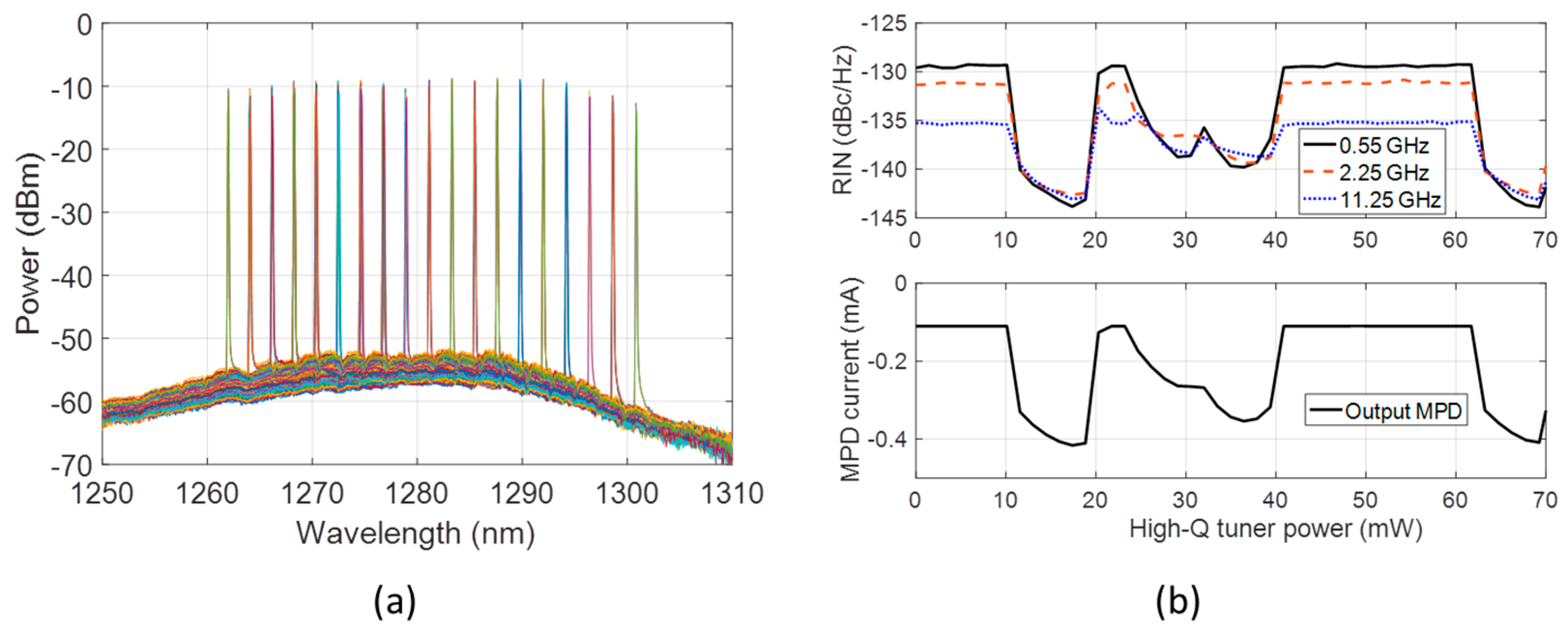
Figure 1.
(a) Add-drop response of single ring resonator (L1 = 200 µm, FSR = 3.31 nm); (b) Vernier of two rings showing 60 nm of free-spectral range (FSR) (L1 = 200 µm, L2 = 211 µm, M = 18.1); Propagation loss is assumed to be 1 dB/cm and all power coupling coefficients are equal to 0.15.
Figure 1.
(a) Add-drop response of single ring resonator (L1 = 200 µm, FSR = 3.31 nm); (b) Vernier of two rings showing 60 nm of free-spectral range (FSR) (L1 = 200 µm, L2 = 211 µm, M = 18.1); Propagation loss is assumed to be 1 dB/cm and all power coupling coefficients are equal to 0.15.

Figure 2.
Typical laser cavity comprising of two ring resonators with slightly different radii forming a single frequency filter (SWF) in between two loop mirrors (R1 and R2) forming a Fabry–Perot cavity. We define effective reflectivity plane Reff to simplify the analysis.
Figure 2.
Typical laser cavity comprising of two ring resonators with slightly different radii forming a single frequency filter (SWF) in between two loop mirrors (R1 and R2) forming a Fabry–Perot cavity. We define effective reflectivity plane Reff to simplify the analysis.

Figure 3.
(a) Effective cavity length calculated for a 3 mm long cavity with SWF from Figure 1b; (b) Longitudinal mode spacing for the same cavity; (c) Phase of the complex amplitude reflectivity reff for the same cavity; (d) Coefficients A, B and F calculated from Equations (8) and (9) for the same cavity. In all cases, the horizontal axis corresponds to the detuning from the resonance.

Figure 4.
Four considered widely-tunable ring-based laser designs. Thermal heaters are drawn in yellow: (a) Ring-bus-ring laser (RBR); (b) Single Coupled-Ring-Resonator laser (CRR 1×); (c) Vernier racetrack resonator and (d) Double Coupled-Ring-Resonator laser (CRR 2×).
Figure 4.
Four considered widely-tunable ring-based laser designs. Thermal heaters are drawn in yellow: (a) Ring-bus-ring laser (RBR); (b) Single Coupled-Ring-Resonator laser (CRR 1×); (c) Vernier racetrack resonator and (d) Double Coupled-Ring-Resonator laser (CRR 2×).

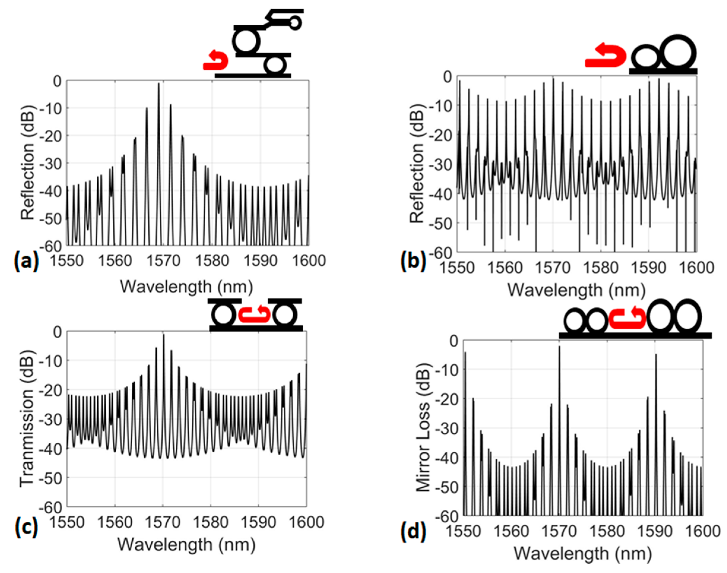
Figure 5.
Synthesized spectra of all the considered ring structures: (a) Ring-bus-ring (RBR) resonator structure; (b) Single Coupled-Ring-Resonator (CRR 1×) structure; (c) Vernier racetrack resonator structure and (d) Double Coupled-Ring-Resonator (CRR 2×) structure.
Figure 5.
Synthesized spectra of all the considered ring structures: (a) Ring-bus-ring (RBR) resonator structure; (b) Single Coupled-Ring-Resonator (CRR 1×) structure; (c) Vernier racetrack resonator structure and (d) Double Coupled-Ring-Resonator (CRR 2×) structure.

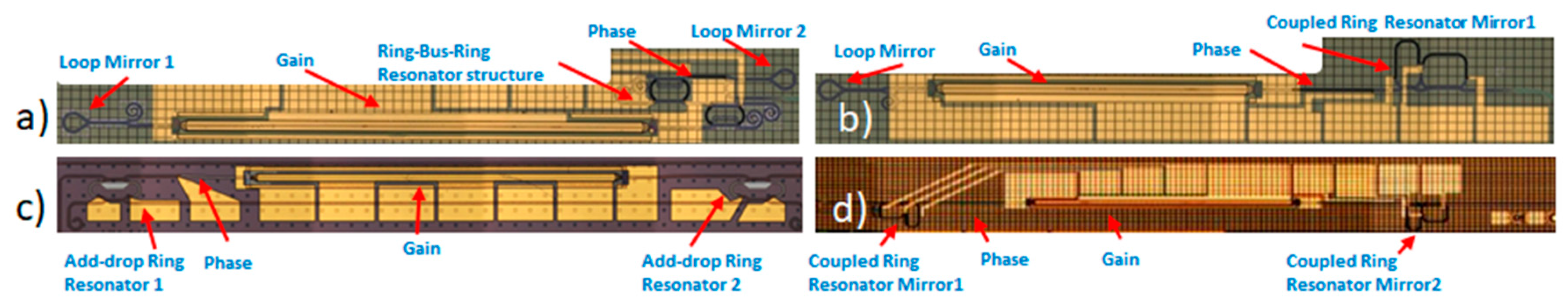
Figure 6.
Optical images of fabricated lasers: (a) Ring-bus-ring laser (RBR); (b) Single Coupled-Ring-Resonator laser (CRR 1×); (c) Vernier racetrack resonator and (d) Double Coupled-Ring-Resonator laser (CRR 2×).
Figure 6.
Optical images of fabricated lasers: (a) Ring-bus-ring laser (RBR); (b) Single Coupled-Ring-Resonator laser (CRR 1×); (c) Vernier racetrack resonator and (d) Double Coupled-Ring-Resonator laser (CRR 2×).

Figure 7.
Plot of peak wavelength vs. ring tuning power for (a) RBR laser; (b) CRR 1× laser; and (c) Vernier racetrack laser. We do not show the CRR 2× laser tuning performance due to unpredictability.
Figure 7.
Plot of peak wavelength vs. ring tuning power for (a) RBR laser; (b) CRR 1× laser; and (c) Vernier racetrack laser. We do not show the CRR 2× laser tuning performance due to unpredictability.

Figure 8.
Measured linewidths for (a) RBR laser; (b) CRR 1× laser; and (c) Vernier racetrack laser. The linewidth of the CRR 2× laser was 196 kHz at the one wavelength where it was measured.
Figure 8.
Measured linewidths for (a) RBR laser; (b) CRR 1× laser; and (c) Vernier racetrack laser. The linewidth of the CRR 2× laser was 196 kHz at the one wavelength where it was measured.

Figure 9.
(a) Tuning map for the RBR laser showing directions of fine (dashed red line) and coarse (dotted blue line) tuning. The black line shows continuous tuning without mode hops, where phase section corrects for the cavity length as wavelength is tuned; (b) The bidirectional lasing nature of the Vernier laser where direction of lasing changes as laser bias is tuned. The clockwise (CW) direction is plotted in blue, and the counterclockwise (CCW) direction in red (similar effect happens with tuning or change of laser operating temperature); (c) Mask layout of CRR structure showing Si waveguides and thermal heaters (green); (d) Reflection from CRR structure when both rings are aligned; (e) Splitting of CRR resonance when two rings have a difference in temperature of 2 °C.

Figure 10.
A schematic view of a tunable laser design with integrated external cavity. Tuners are yellow (two phase sections and two rings for wide tuning), and SOAs are dark orange (gain section inside the laser cavity, and external SOA that is used to control the level of feedback). The output monitor photodiode (MPD) is used to measure the laser output power for adjustment of laser parameters.
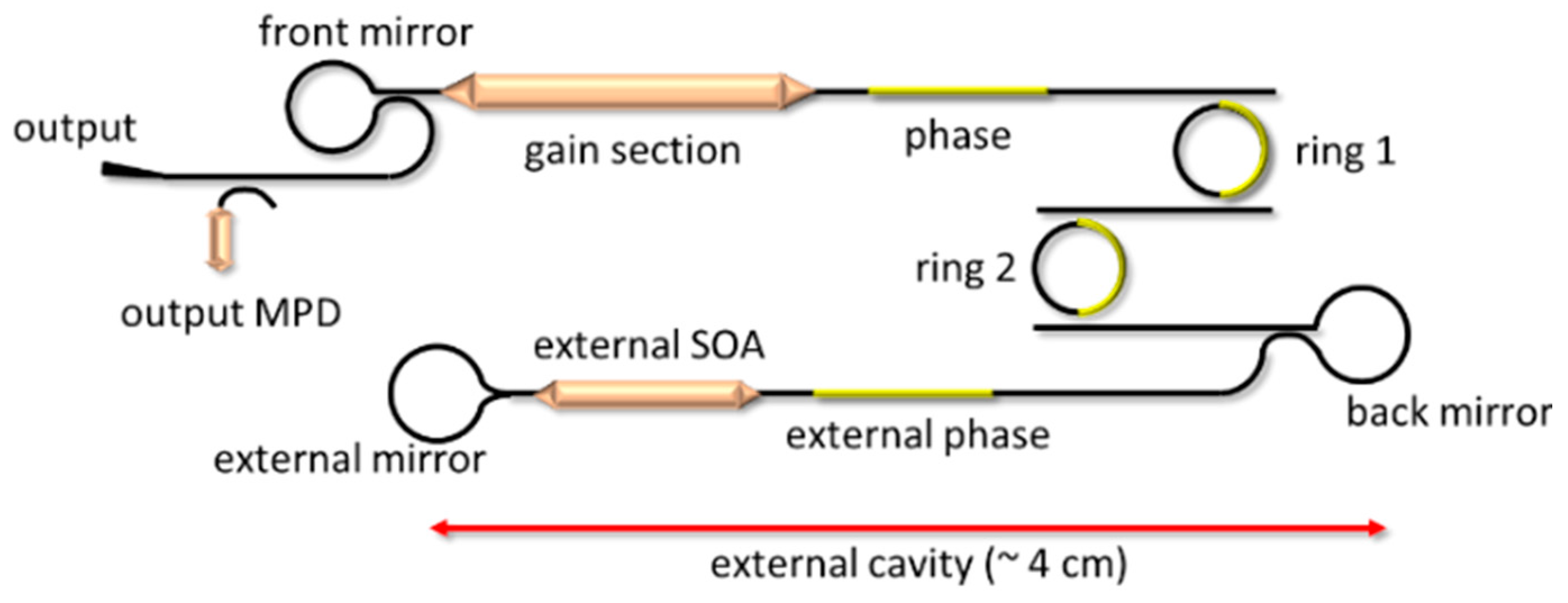
Figure 11.
(a) The influence of feedback from external cavity when SOA is biased at 0 V. The x-axis is the squared current (I2~P) applied to external cavity phase tuner, the y-axis is the current collected by monitor photodetector (MPD) at the laser output and every curve corresponds to different laser bias between 30 and 80 mA in steps of 1 mA; (b) Measured linewidth across the full tuning range. The horizontal line shows the linewidth measured on similar laser structure with no external cavity.

Figure 12.
(a) Schematic of external cavity laser with high-Q ring in all-pass configuration; (b) Schematic of external cavity laser with high-Q ring in add-drop configuration.
Figure 12.
(a) Schematic of external cavity laser with high-Q ring in all-pass configuration; (b) Schematic of external cavity laser with high-Q ring in add-drop configuration.

Figure 13.
(a) Schematic of laser with high-Q ring inside the cavity; (b) Ring 1 and 2 provide for wide-tunability due to Vernier effect, and filter-out a single resonance of ring 3.
Figure 13.
(a) Schematic of laser with high-Q ring inside the cavity; (b) Ring 1 and 2 provide for wide-tunability due to Vernier effect, and filter-out a single resonance of ring 3.

Figure 14.
(a) Schematic of laser with high-Q ring inside the cavity that includes two monitor photodetectors and a booster SOA (BSOA); (b) A probed laser bar on a stage comprising of a number of laser structures. A single device with high-Q ring inside the cavity occupies an area of ~4 mm2.
Figure 14.
(a) Schematic of laser with high-Q ring inside the cavity that includes two monitor photodetectors and a booster SOA (BSOA); (b) A probed laser bar on a stage comprising of a number of laser structures. A single device with high-Q ring inside the cavity occupies an area of ~4 mm2.

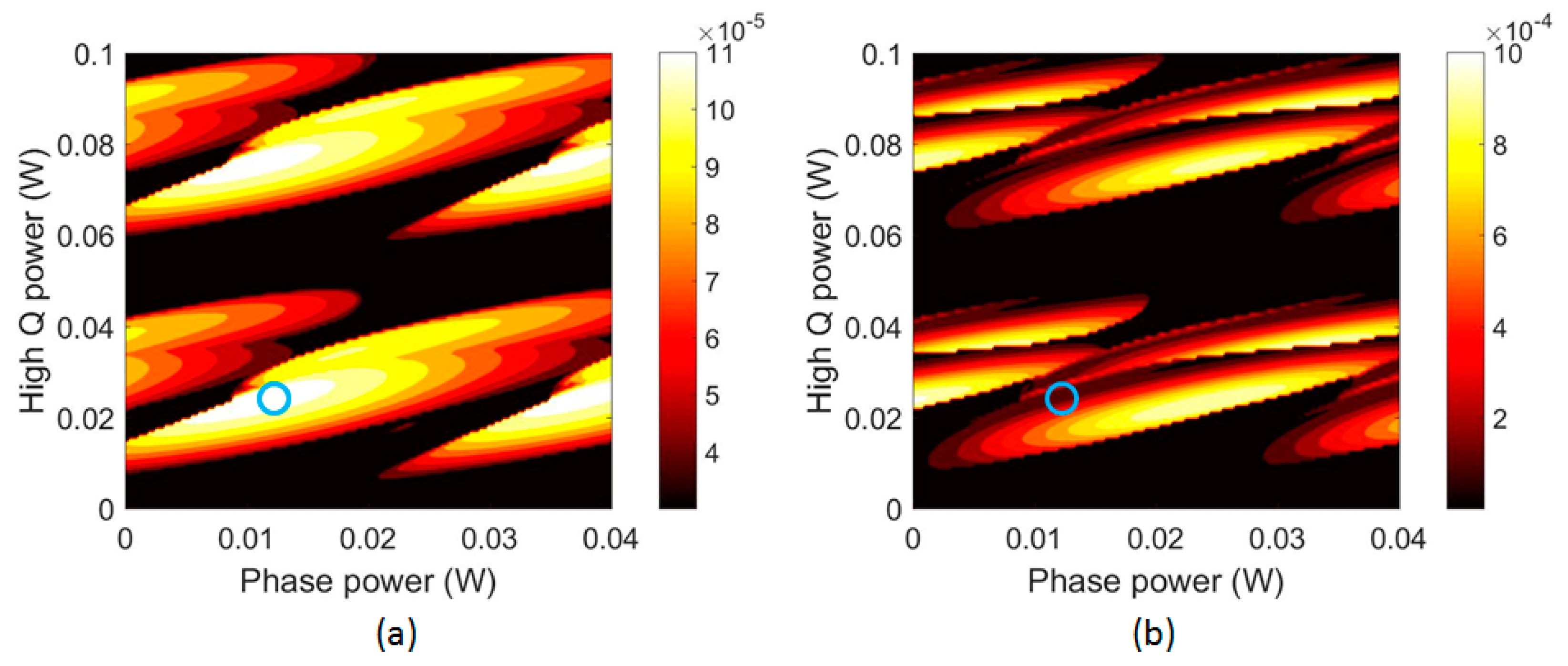
Figure 15.
Monitor photodetector current for the (a) output MPD; and (b) high-Q ring MPD as a function of heater power delivered to phase section and high-Q ring. The blue rings show the region of maximum output power in (a) and identical position for the high-Q monitor that is in the local minimum (b).

Figure 16.
(a) Optical spectra as one of the Vernier rings is tuned and high-Q ring and phase are adjusted for maximum current at the output monitor photodetector; (b) Correlation between laser relative intensity noise (RIN) measured at 0.55, 2.25 and 11.25 GHz, and monitor photodetector currents, as high-Q ring is swept. RIN is optimized when output power is maximized.

Figure 17.
Widely-tunable integrated lasers linewidth versus time. We make a distinction between III/V based monolithic lasers, hybrid lasers where III/V gain chips are butt coupled to Si or SiN chips, and heterogeneous integrated lasers where the III/V gain material is bonded to silicon. (sampled grating distributed bragg reflector (SG-DBR) lasers, distributed feedback (DFB) lasers and micro-ring resonator (MRR) lasers).
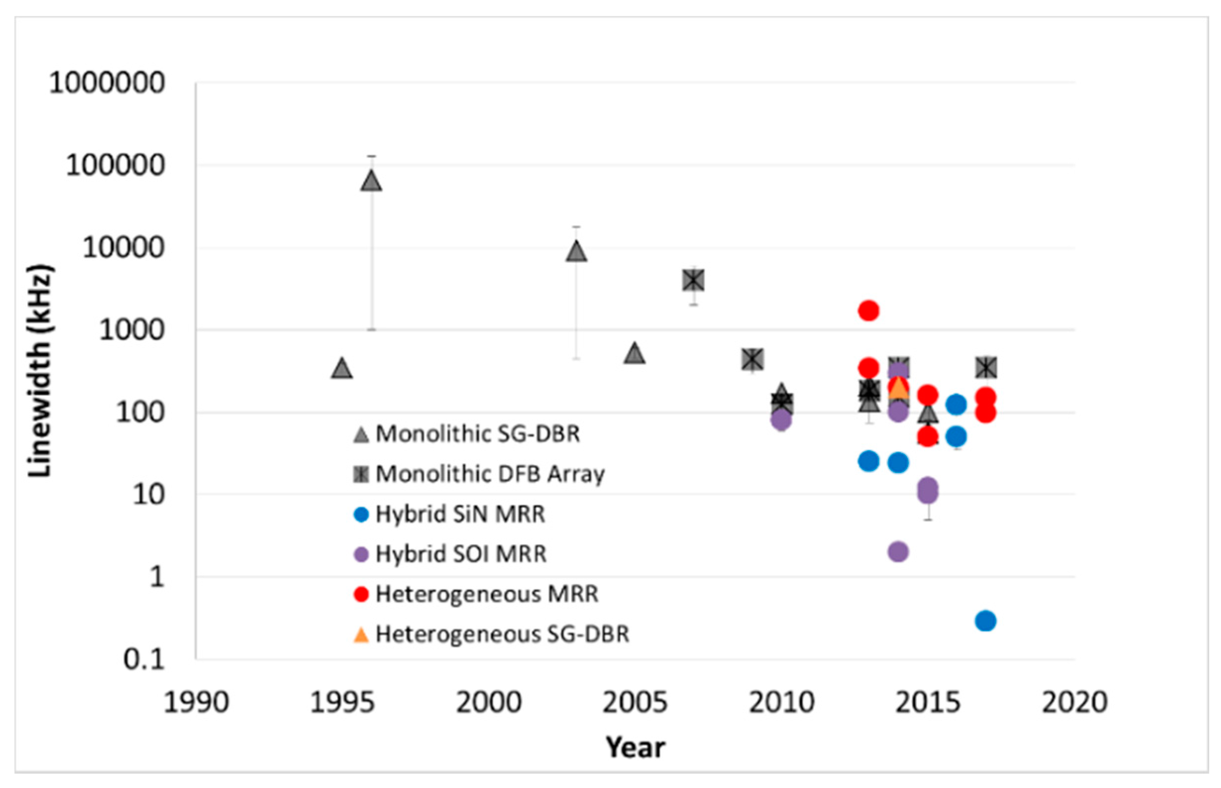
© 2017 by the authors. Licensee MDPI, Basel, Switzerland. This article is an open access article distributed under the terms and conditions of the Creative Commons Attribution (CC BY) license (http://creativecommons.org/licenses/by/4.0/).
Share and Cite
MDPI and ACS Style
Komljenovic, T.; Liang, L.; Chao, R.-L.; Hulme, J.; Srinivasan, S.; Davenport, M.; E. Bowers, J. Widely-Tunable Ring-Resonator Semiconductor Lasers. Appl. Sci. 2017, 7, 732. https://doi.org/10.3390/app7070732
AMA Style
Komljenovic T, Liang L, Chao R-L, Hulme J, Srinivasan S, Davenport M, E. Bowers J. Widely-Tunable Ring-Resonator Semiconductor Lasers. Applied Sciences. 2017; 7(7):732. https://doi.org/10.3390/app7070732
Chicago/Turabian StyleKomljenovic, Tin, Linjun Liang, Rui-Lin Chao, Jared Hulme, Sudharsanan Srinivasan, Michael Davenport, and John E. Bowers. 2017. "Widely-Tunable Ring-Resonator Semiconductor Lasers" Applied Sciences 7, no. 7: 732. https://doi.org/10.3390/app7070732
Note that from the first issue of 2016, this journal uses article numbers instead of page numbers. See further details here.