
Perfect Light Absorbers Made of Tungsten-Ceramic Membranes


National Institute for Materials Science (NIMS), 1-1 Namiki, Tsukuba 305-0044, Japan
Appl. Sci. 2017, 7(5), 458; https://doi.org/10.3390/app7050458
Submission received: 8 March 2017
/
Revised: 21 April 2017
/
Accepted: 26 April 2017
/
Published: 29 April 2017
(This article belongs to the Special Issue Guided-Wave Optics)
Abstract
:Plasmonic materials are expanding their concept; in addition to noble metals that are good conductors even at optical frequencies and support surface plasmon polaritons at the interface, other metals and refractory materials are now being used as plasmonic materials. In terms of complex permittivity at optical frequencies, these new plasmonic materials are, though not ideal, quite good to support surface plasmons. Numerical investigations of the optical properties have been revealing new capabilities of the plasmonic materials. On the basis of the precise computations for electromagnetic waves in artificially designed nanostructures, in this article, we address membrane structures made of tungsten and silicon nitride that are a typical metal and ceramic, respectively, with high-temperature melting points. The membranes are applicable to low-power-consuming thermal emitters operating at and near the visible range. We numerically substantiate that the membranes serve as perfect light absorbers, in spite of the subwavelength thickness, that is, 200–250 nm thickness. Furthermore, we clarify that the underlying physical mechanism for the unconventional perfect absorption is ascribed to robust impedance matching at the interface between air and the membranes.

1. Introduction
Membrane structures can be used to manipulate light in outstanding ways. One example is photonic crystals made of high-refractive index materials such as semiconductors [1]. However, such membrane structures are generally fragile and difficult to handle since they are free-standing in air and have thickness less than the wavelength of light in vacuum, that is, subwavelength. Today, ceramic membranes can be realized, thanks to reliable thin-film fabrication techniques such as plasma-enhanced chemical vapor deposition. Here, we focus on membrane structures based on free-standing thin films made of ceramics. To make the application clear, we design perfect light absorbers (PLAs) suitable for thermal emitters in the short-wavelength infrared range of 1–2 m. Thermal emitters made of nanostructured materials are currently optimized for the mid-infrared range of 2–5 m, using metal-insulator-metal structures that typically comprise noble metals [2,3,4,5], aluminum [6], etc., as constituent materials; however, these metals cannot withstand high temperatures.
A basic requirement exists for the thermal emitters, that is, high melting points exceeding 2000 K. From this point of view, we chose silicon nitride (SiN) as the ceramic and tungsten (W) as the metal in this study. Both of them are stable at high temperatures. Considering practical application, the thickness of SiN membranes and W are assumed to be 100–200 nm and 50–100 nm, respectively, which are usual values in commercial products [7] and laboratory use. A 3D photonic crystal made of only W was once produced with a similar goal as mentioned above and worked as a thermal emitter at about 2 m [8]. However, production of thermal emitters based on such structures still has a high demand and has not been standardized to date; thus, much simpler structures are highly preferred from the viewpoint of practical application.
Light absorbers in infrared ranges have a long history. Originally, the idea to obtain PLAs was simple; that is, to use materials as analogous to black bodies as possible. The absorbed infrared light has been converted to electric signals since the 1940s [9]; the devices are well known as conventional bolometers. However, it has been difficult to attain PLAs over the whole wavelength range. Accordingly, PLAs based on the artificially designed structures were conceived for the particular wavelength ranges [2,3,4,5,6]; in fact, the PLAs do not look like black bodies. Thus, there are distinct differences between black-body-based and artificial-structure-based PLAs.
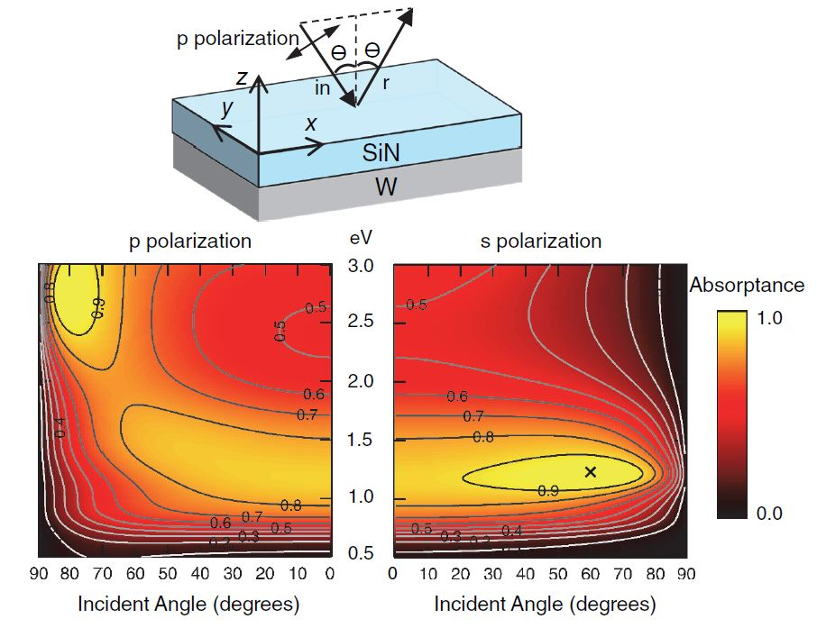
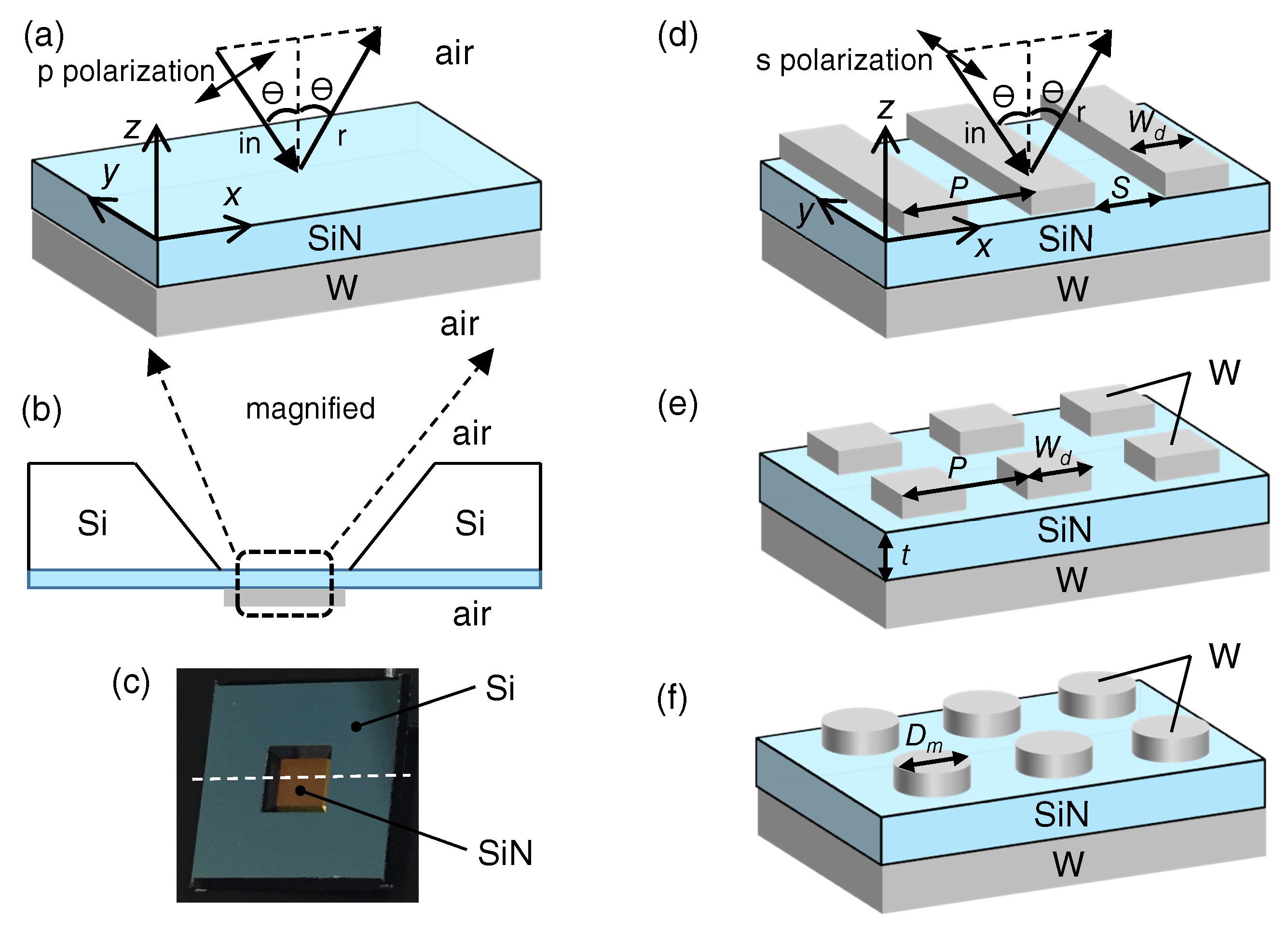
Figure 1 illustrates schematics of W-SiN membrane structures studied in this work. Figure 1a–c shows simply stacked W and SiN layers. The two-layer membrane structure is formed using a SiN membrane on a Si substrate. The section view is shown in Figure 1b. The image of the original SiN membrane is shown in Figure 1c; the central square domain of mm2 is the SiN membrane. Once deposition of W is performed, the W-SiN membrane structure in Figure 1a,b is obtained. The white dashed line indicates a section corresponding to Figure 1b. Figure 1a also indicates the coordinate axes and optical configuration of p polarization, which is defined such that the incident polarization vector is parallel to the plane of incidence. Without loss of generality, we set the plane of incidence to be parallel to the xz plane.
Figure 1d–f shows schematics of W-SiN-W membrane structures, whose top layers are set to be periodic. Figure 1d also shows the coordinate axes and s polarization. When the plane of incidence is parallel to the xz plane, s polarization means that the incident polarization is perpendicular to the xz plane and parallel to the y-axis. Figure 1d shows a 1D periodic structure along the x axis. Figure 1e,f shows 2D periodic structures of square arrays of W patches; we set the coordinate axes to be similar to Figure 1d. In Figure 1d–f, we define notations P, S, , and for the periodic lengths, slit length, width of the W bars or square patches, and diameter of the circular W patches, respectively.
In the optical linear response regime, light absorptance A is evaluated using the following equation:
where and denote the mn-th reflective and transmissive diffraction, respectively. and are ordinary reflectance (R) and transmittance (T), respectively. As we describe in detail in Section 3.2, the linear optical responses of and are directly computed in a numerically precise way, based on Maxwell equations. Note that Equation (1) is represented in the range where 0 and 1 denote 0% and 100%, respectively.
Perfect light absorption is related to perfect emittance by reciprocity [10]; therefore, when thermal emitters were produced, researchers tried to attain perfect-absorption structures [2,3,4,5,6]. Recently, nearly perfect absorption was observed in stacked complementary structures [11], which show significant enhancement of electric-dipole emission loaded on the outmost surfaces [12,13,14]. In addition, it was lately reported that high-emittance plasmonic cavities substantially enhance both electric- and magnetic-dipole emissions of Er ions [15]. Thus, it has been quite common to relate efficient light absorption with high emittance.
In this study, we aim at designing PLAs made of a set of representative refractory metal and ceramic, based on precise numerical calculations. To propose realistic designs, we conduct the numerical calculations using reliable material parameters. As for the metal W, the complex relative permittivity is taken from the literature [16], and, as for the ceramic SiN, we adopt a representative value, that is, permittivity of 4.3. Further details are provided in Section 3.1. The representative value is sufficient to extract fundamental properties of the W–ceramic systems. We show that the W-SiN membranes are able to serve as PLAs even when they have subwavelength thickness, suggesting that they can function as low-power-consumption thermal emitters near the visible range. We also clarify that the working mechanism of the PLAs is unconventional, robust, and different from that of noble-metal–insulator systems studied so far [2,3,4,5,6].
2. Results and Discussion
In this section, we show numerical results for PLAs made of W and SiN. Periodic structures are introduced to absorb incident light efficiently in the very thin membrane structures of subwavelength thickness. Below, we confirm the basic optical properties of the constituent materials.
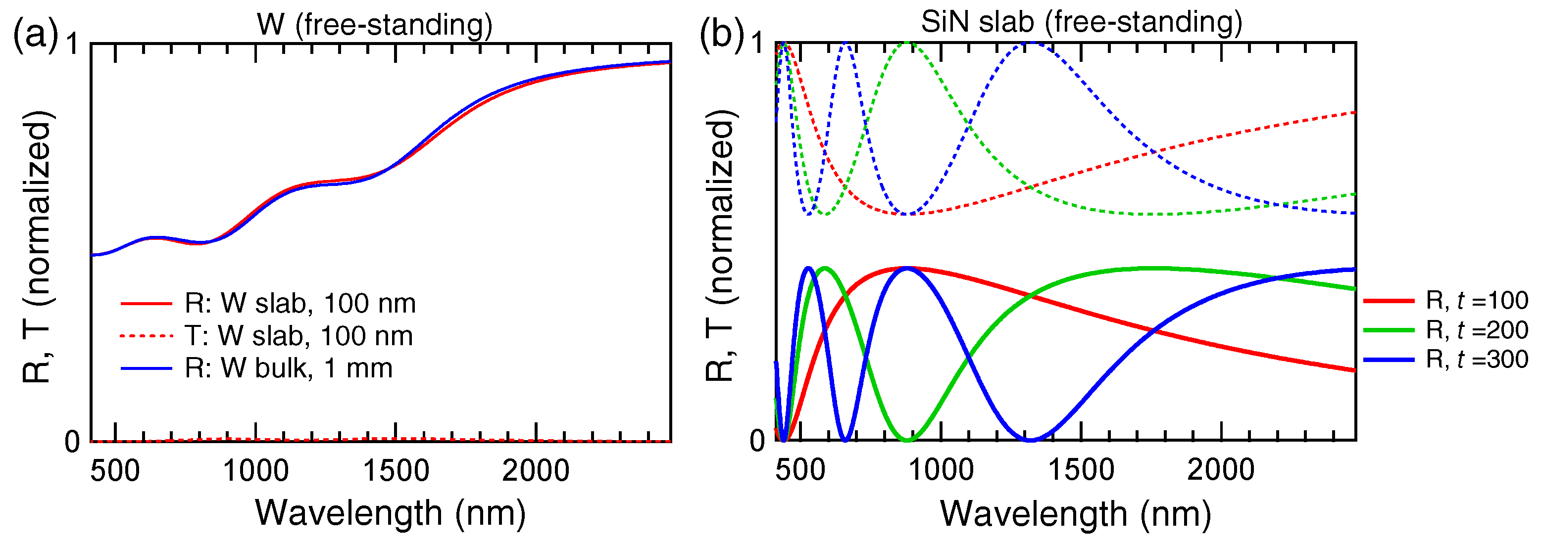
Figure 2 shows the basic optical properties of W and SiN. Figure 2a presents R and T spectra of W membrane with red solid and dashed lines, respectively. The W membrane is assumed to be free standing in air. The spectra are shown in the scale. Note that the T spectrum is close to 0 in the whole wavelength range shown. Figure 2a also shows R spectrum of bulk W of 1 mm thickness with blue curve, which is almost identical to the R spectrum of the W membrane. This means that the W membrane of 100 nm thickness is optically thick enough, being almost equivalent to bulk W in terms of the optical properties.
As for the spectral shapes of the W membrane in Figure 2a, R decreases as the wavelength becomes shorter. For example, at 500 nm, R is 0.48 and, at 1000 nm, R is 0.58. In comparison with a noble metal Ag, the R values are quite small. This means that W is associated with substantially large optical loss even at the near-infrared range.
Figure 2b shows R and T spectra of SiN membranes of thickness , 200, and 300 nm with red, green, and blue curves, respectively. The R and T spectra are shown with solid and dashed curves, respectively. The SiN membranes were assumed to be free-standing in air. The spectral shapes manifest the Fabry–Perot-type interference that is determined by the refractive index and thickness. Since we are assuming loss-less refractive index, light absorption does not take place at all in the SiN membranes.
2.1. Nearly PLA of Simply Stacked W-SiN Membrane
Figure 3 shows typical results on light absorption and electromagnetic (EM) fields in a simply stacked W-SiN membrane. The schematic is shown in Figure 1a. We fix the thickness of the W and SiN layers to be 100 nm because we intend to elucidate representative properties of the two-layer membrane.
Figure 3a,b shows 2D color and contour plots of light absorptance under p and s polarizations, respectively. The horizontal and vertical axes represent incident angles and photon energy in eV, respectively. Note that the normal incidence of 0° is in common with the two polarizations. The absorptance was evaluated using Equation (1). High absorptance of more than 0.8 (or 80%) appears both at p and s polarizations in the 1.0–1.5 eV (that is, 1239.5–826.3 nm in wavelength) range including the normal incidence. Perfect absorption also appears both at p and s polarizations; under p polarization, it is located around 78° and 2.8 eV, and, under s polarization, it is around 60° and 1.2 eV.
Figure 3a,b explicitly shows perfect absorption by the two-layer W-SiN membrane. Multilayers of noble metals and insulators have been studied since the 1960s [17,18]. Although several papers reported experimental observations of the optical responses [19,20,21,22,23], perfect light absorption, to our best knowledge, has not been observed in the noble-metal–insulator multilayer membranes. Thus, the optical response of the two-layer W-SiN membrane turns out to be unconventional.
Figure 3c,d shows snapshots of electric-field distributions under conditions of large light absorption; each condition is indicated by open circle (∘) and cross (×), respectively, in Figure 3b. The corresponding incident angles are and . Under both conditions, the incident polarization was s polarization; accordingly, the component is plotted with blue-to-red colors in Figure 3c,d. We set the incident equal to 1.0. The incident light propagates from the top. The interfaces of air/SiN, SiN/W, and W/air are shown with green lines.
Figure 3e,f corresponds to Figure 3c, and shows the absolute value of electric field and the profile along the z-axis, respectively. The green lines indicates the interfaces, similarly to Figure 3c. We set the interface of air/SiN at . Note that Figure 3f is plotted in decreasing order on the horizontal axis. Obviously, the electric field rapidly decays inside the two-layer W-SiN membrane; in other words, it is efficiently absorbed in the membrane. From Equation (1), perfect absorption () requires , which is often called impedance matching. Under the open-circle condition in Figure 3b, although the absorptance is not exactly equal to 1, the electric-field distribution is qualitatively understood to be due to impedance matching and does not arise from a plasmonic resonance.
Figure 3g,h corresponds to Figure 3e,f, and shows the absolute value of magnetic field and the profile along the z axis, respectively. The profile takes the maximum value at the W/SiN interface. We mention that the magnetic-field distribution is uniquely determined by the boundary-connection conditions in the membrane structure and that light absorption mostly takes place in the W layer through one of Maxwell equation,
where is permittivity in vacuum because spatial distribution of is directly affected by the complex relative permittivity in the W layer (); the permittivity has a large imaginary part [16] that is associated with optical loss.
Figure 3i,j corresponds to Figure 3d and shows the distributions in a similar way to Figure 3e,f. Also under the oblique incidence (× in Figure 3b), the profile indicates efficient light absorption.
Figure 3k,l corresponds to Figure 3i,j, and shows the distribution and the z profile, respectively. Qualitatively, the descriptions for Figure 3g,h are true for Figure 3k,l as well.
In short, the large light absorption at 1.0–1.5 eV and wide incident angles including is ascribed to impedance matching of the two-layer membrane structure. The efficient absorption primarily originates from the property of W permittivity. We point out that the single layer of W does not realize efficient light absorption as shown in Figure 2a. In this sense, the two-layer membrane structure is the minimal requirement for large light absorption in W–ceramic systems.
2.2. 1D Periodic PLAs Made of W-SiN-W Membranes
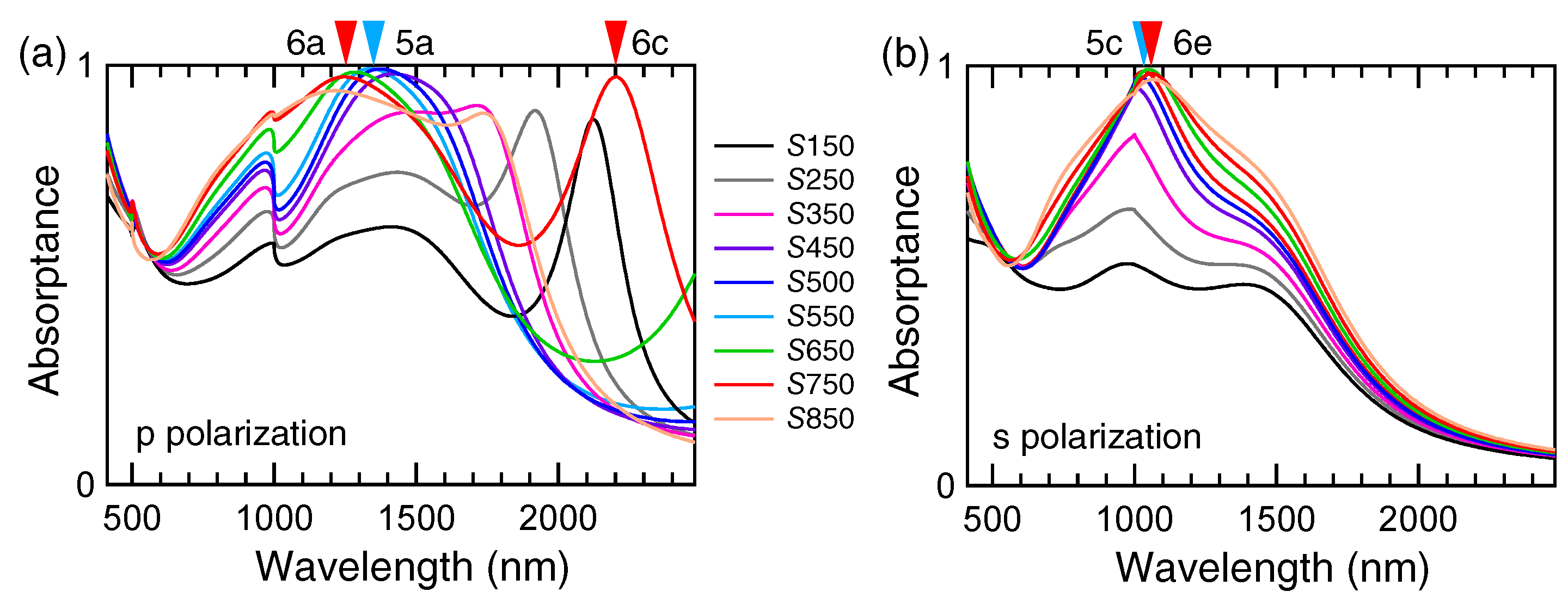
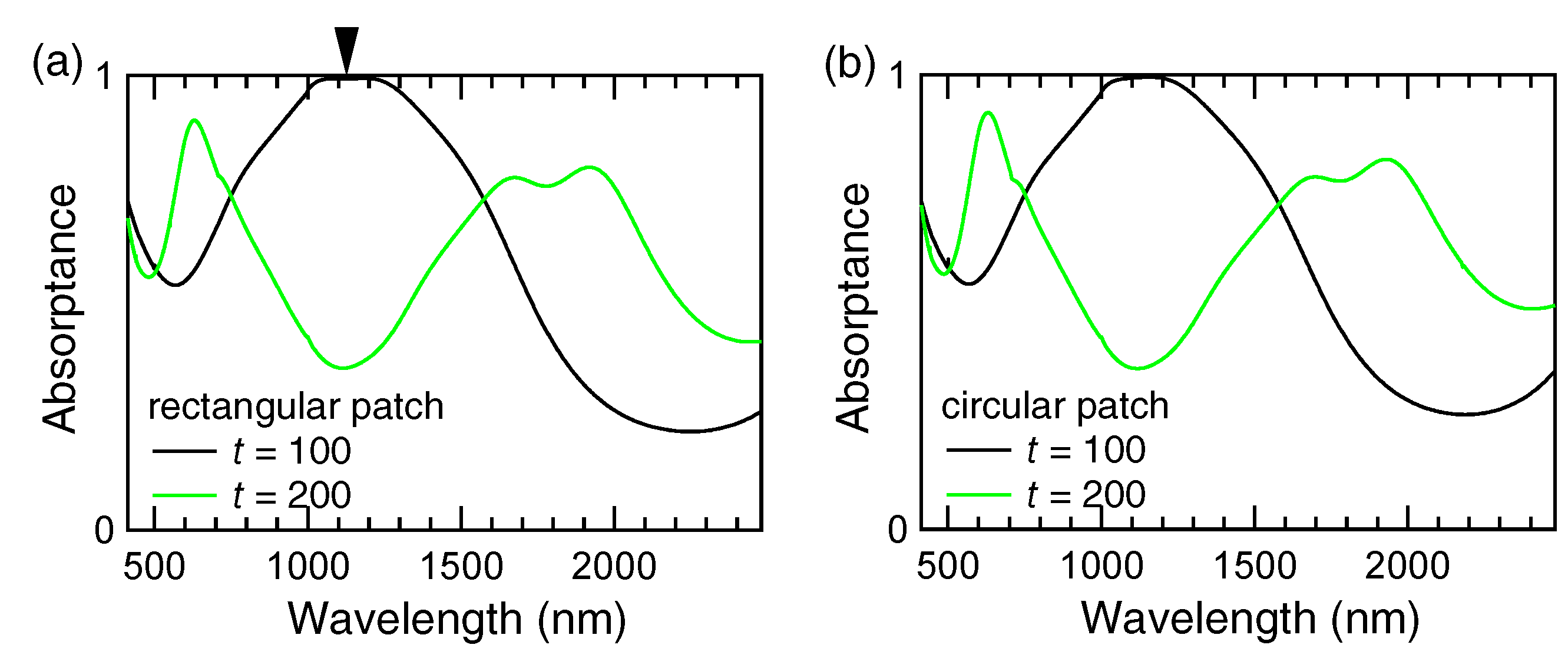
Figure 4 shows absorptance spectra of on-top 1D periodic W-SiN-W membranes. The schematic is shown in Figure 1d. We set the periodicity P to be 1000 nm and the incidence was set to be normal; we found signatures of diffraction at 1000 nm such as small steps in Figure 4a and kinks in Figure 4b. Various absorptance spectra represent light absorption in the 1D periodic W-SiN-W membranes with different widths of air slit S, which was varied from 150 to 850 nm. Accordingly, the width of metal, , was varied from 850 to 150 nm because . The linear optical responses ( and ) were numerically computed and the absorptance was evaluated using Equation (1).
As S increases under p polarization in Figure 4a, the absorptance spectra for (purple curve) to 750 nm (red curve) have perfect-absorption peaks around 1300 nm. For nm, another nearly perfect-absorption peak appears at 2200 nm, whose signature is seen for nm (green curve) at the longest wavelength edge.
As S increases under s polarization in Figure 4b, the absorptance gradually increases and reaches almost 1 for nm (blue curve), and keeps the perfect absorption at approximately 1050 nm for larger S.
Color cones in Figure 4 indicate some of the perfect-absorption peaks for which we next examine the EM fields. Symbols such as 5a and 6a associated with the color cones denote the corresponding EM distributions shown in Figure 5a and Figure 6a, respectively.
Figure 5 presents EM-field distributions at perfect-light-absorption conditions of 1D W-SiN-W membranes with air slit nm and width of the metal nm. The incidence conditions of polarization and wavelength are indicated in Figure 4 with the sky-blue cones. The absolute values and are shown in linear scale in the minimum-to-maximum-value manners.
Figure 5a,b shows an xz-section view of and distributions under the incidence condition indicated by the sky-blue cone in Figure 4a (p polarization and 1350.2 nm). The incidence was normal, being normalized such that the incident and . The boundaries of the involved materials are shown with green lines, except for the air/W boundary in Figure 5a because of the high contrast and to avoid concealing small hot spots by the lines. The electric field is locally amplified at the W corners, exhibiting the small hot spots, whereas the magnetic field is localized at the flat SiN/W interface. The profile is quite similar to the two-layer system in Figure 3. We point out that the so-called gap mode in the W-SiN-W structure is not responsible for the perfect absorption.
Figure 5c,d shows the and distributions in the xz section under another perfect-absorption condition, indicated by the sky-blue cone in Figure 4b (s polarization and 1032.1 nm). Then, the incident polarization vector is parallel to the y-axis and satisfies ; accordingly, the incident . Figure 5c shows that there is no hot spot and the electric field reaches the bottom W layer unless the top W bar interrupts the propagation. Figure 5d shows that the magnetic field is mainly enhanced at the flat SiN/W interface, similarly to Figure 5b. Thus, in this 1D periodic system of nm, the perfect absorption takes place with a mechanism similar to that in the two-layer membrane structure. It is to be stressed that, even though the structure is certainly anisotropic in the 1D periodic W-SiN-W membrane, the perfect-absorption mechanism is primarily independent of the incident polarizations and the structural anisotropy.
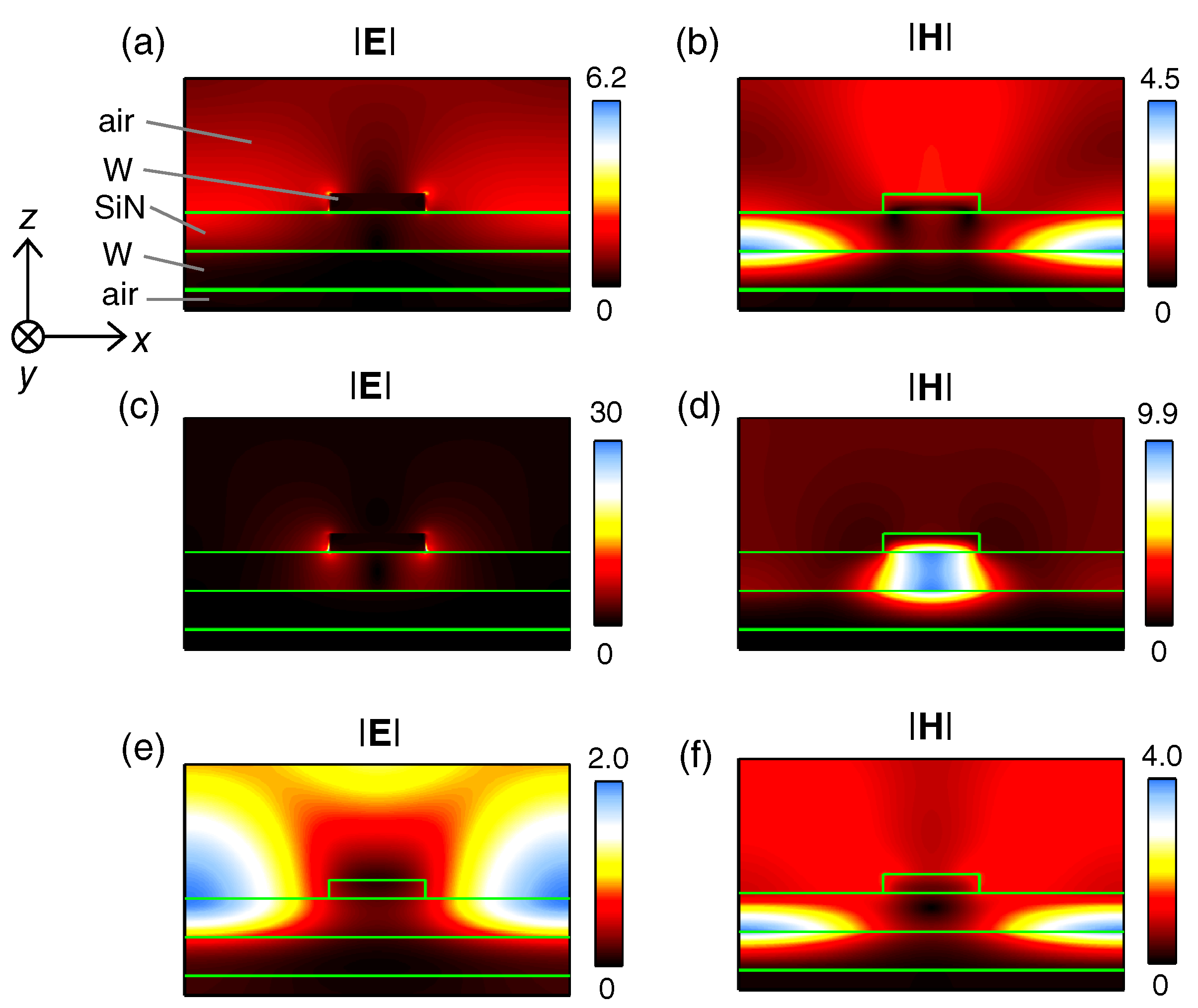
Figure 6 displays EM-field distributions at perfect-light-absorption conditions of 1D W-SiN-W membranes with air slit nm and width of the metal nm. The corresponding absorptance spectra are shown with the red curves in Figure 4 and the three nearly perfect-absorption peaks are indicated by the red cones. Green lines indicate the boundaries of the 1D periodic membrane, similarly to Figure 5.
Figure 6a,b shows the and distributions, respectively, under p polarization and 1252.0 nm. The EM-field distributions are qualitatively similar to those in Figure 5a,b, irrespective of the substantial difference in air slit S.
Figure 6c,d shows the and distributions, respectively, under the condition of p polarization and 2201.6 nm, which correspond to nearly perfect absorption sensitive to S. We note that only the scale in Figure 6c is shown in a peak-cut way; that is, although the maximum value of in Figure 6c is 64, the scale is set to have the maximum at 30 and the locations exceeding 30 are represented in sky blue. Qualitatively, the EM-field distributions are distinct from those in Figure 6a. The electric- and magnetic fields show strong localization around the W-SiN-W gap. It is obvious that the distribution takes the maximum value in the gap. These EM-field distributions are peculiar to the gap mode or plasmonic waveguide mode [12]. Thus, it is found that the plasmonic gap mode appears at a particular condition, being sensitive to the structural parameters.
2.3. 2D Periodic PLAs Made of W-SiN-W Membranes
Figure 7a,b shows absorptance spectra of 2D periodic W-SiN-W membranes of on-top rectangular and circular patches, respectively. The schematics are shown in Figure 1e,f. Each panel in Figure 7 presents two spectra for the 2D periodic membranes with periodicity nm and the middle SiN-layer thickness and 200 nm, which are shown with black and green curves, respectively. One side of the W square was set to nm and the diameter of the circular W was nm, where was chosen to keep the volume of the circular patch equivalent to that of the square one. The thickness of the top and bottom layers of W was set to 50 and 100 nm, respectively. Quantitatively, they exhibit similar absorptance spectra, irrespective of the difference of the patch shapes.
One common feature in Figure 7a,b is that perfect-absorption bands appear at 1050–1200 nm. We note that, in the 1D periodic membranes in Figure 4, the perfect absorption appears as peaks (not band). This feature is due to the 2D periodic structures and probably originate from the dimensionality. The cone at 1126.8 nm in Figure 7a indicates the wavelength corresponding to EM-field distributions in the next Figure.
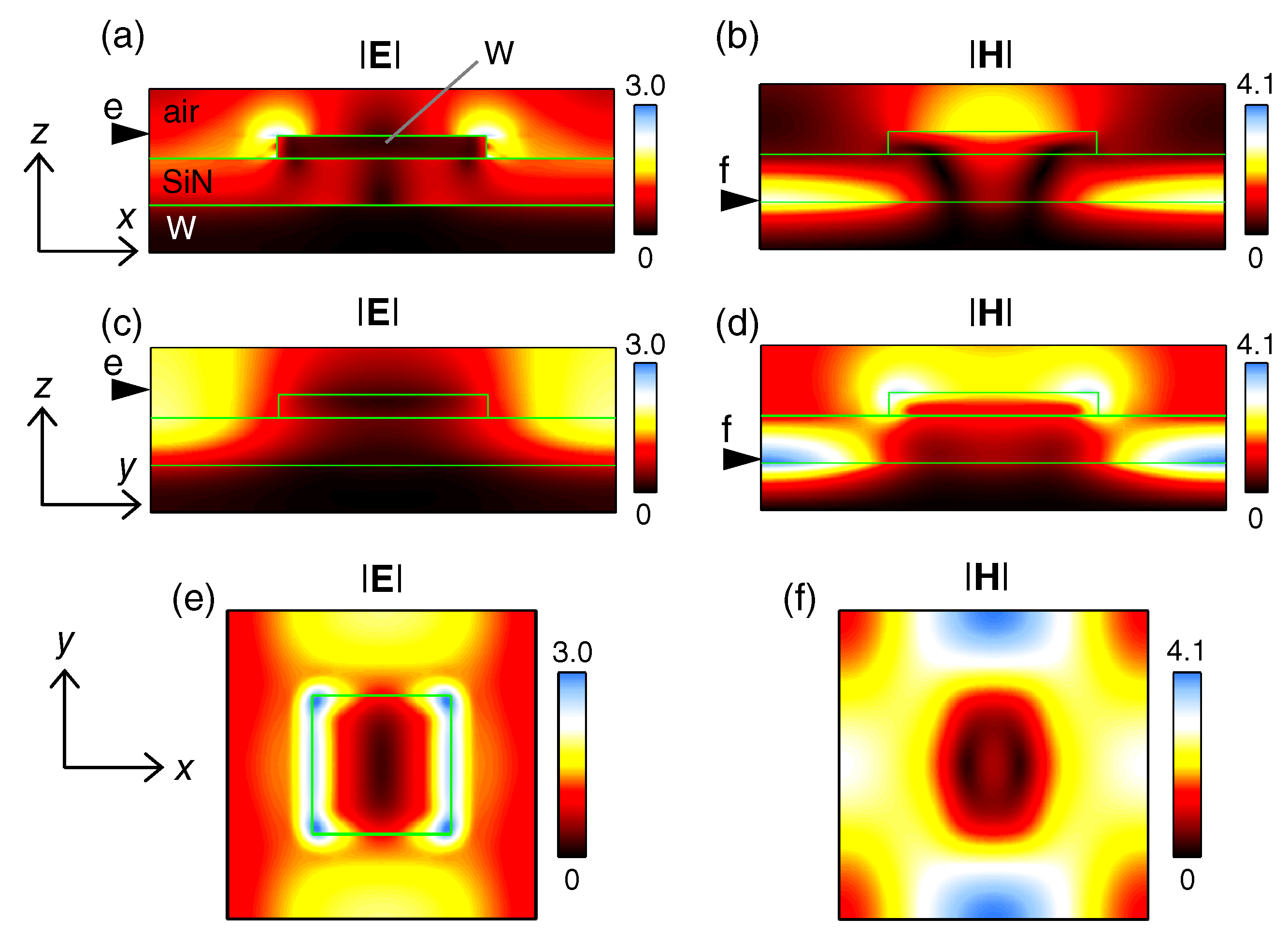
Figure 8 shows a set of EM-field distributions of the 2D periodic W-SiN-W membrane at a perfect-absorption condition indicated by the cone (1126.8 nm) in Figure 7a. The incidence was set to be normal and to have and . Note that the scales for and are in common to provide systematic views. Green lines indicate the boundaries in the 2D membrane.
Figure 8a,b shows the and distributions, respectively, in a xz section that cut through the center of the on-top square W patch. The incident polarization vector is parallel to the x-axis and induces hot spots at the corner of the W patch. The distribution takes larger values than the incidence at the interfaces of air/W and SiN/W.
Figure 8c,d shows the corresponding yz-section view through the center of the on-top square W patch. The distribution does not include any hot spot whereas the distribution is strongly localized at the SiN/W interface, being scattered at the corner of the on-top W patch.
Figure 8e displays an xy-view distribution at a representative z position, which was set to be 1 nm above the air/W interface and indicated by the cones in Figure 8a,c. The position of the square W patch is shown with green lines for better visibility. The distribution takes the maximum value at the corners of the W patch and mainly localizes around the W patch.
Figure 8f shows an xy-view distribution at a representative z position, which was set to be 1 nm above the interface of the SiN/W and indicated by the cones in Figure 8b,d. The distribution is mostly enhanced at the positions between the on-top W patches and localizes at the SiN/W interface. Thus, it is found that the perfect-absorption band is realized by the combination of local electric-field scattering by the on-top W patch and magnetic-field localization at the SiN-W interfaces. The local scattering can be interpreted as local plasmon at the rectangular W nanostructures and includes substantial longitudinal components that are usually excited as continuum [12] and are considered to realize the perfect-absorption continuum. In terms of the structures, the 1D structures in Figure 4 do not have the rectangular corners in the xy plane and therefore do not tend to form perfect-absorption continuum.
3. Materials and Methods
3.1. Material Parameters
As for the metal W, the complex relative permittivity is taken from the literature [16], in which the measured data were well fitted by the Lorentz–Drude model over a wide wavelength range including the range of interest in this study. Therefore, we use the complex permittivity approximated by the model.
As for the ceramic SiN, although literature is available [24], the measured data are quite sparse in the near-infrared range of interest. Therefore, we adopt a representative value, that is, a permittivity of 4.3. Although there is slight wavelength dispersion in the range of present interest, the representative value is sufficient to extract fundamental properties of the W–ceramic systems. In addition, the representative value is a good approximation for other ceramics such as Ta2O5 and allows us to consider other alternatives for ceramics.
3.2. Numerical Method
Here, we employed the rigorous coupled-wave analysis (RCWA) method to compute the optical responses and EM field distributions of the different PLA structures. To evaluate the optical responses of the periodic structures in the frequency domain, the RCWA method is suitable and one of the most reliable methods because it directly solves Maxwell equations for the periodic structures in a numerical manner without any simplification and modelling. The RCWA method was originally formulated in the frequency domain, using Fourier transformation from the spatial coordinate to the wavenumber space and was substantially improved in the truncation order of the Fourier expansion [25].
To handle stacked structures, it is important to incorporate the scattering-matrix algorithm in order to avoid numerical divergence that makes the numerical calculations impossible [26]. The optical spectra and the resultant absorptance spectra were obtained based on the RCWA method incorporating the scattering-matrix algorithm, which was implemented in a multi-parallel manner on supercomputers.
4. Conclusions
We have numerically examined several W-SiN membrane structures and demonstrated that they are able to serve as PLAs in the short-wavelength infrared range. The unconventional mechanism of perfect light absorption has been revealed and was ascribed to the robust impedance matching of the membranes to air, irrespective of the dimensionality. We also showed that the minimal requirement for the nearly perfect absorption is the two-layer W-SiN membrane. In addition, the plasmonic waveguide mode was observed in the 1D periodic W-SiN-W membrane with a particular structural parameter. The 1D and 2D periodic structures were found to be useful to obtain perfect absorption though their fabrication is more complicated, compared to the simple two-layer membrane. Overall, the W-SiN membranes are found to be practical solutions for thermal emitters working near the visible range. On the basis of the present designs, we would fabricate low-power-consuming thermal devices emitting visible and near-infrared light.
Acknowledgments
The author is grateful to Hideki T. Miyazaki (NIMS) for discussions and suggestions, and thanks financial support from KAKENHI Grant (No. 26706020) and from the 4th mid-term research project in NIMS. The author also thanks the High-Performance Computing Infrastructure (HPCI) system research project (ID: hp160035) for the support with the numerical implementations at Cyberscience Center, Tohoku University.
Conflicts of Interest
The author declares no conflict of interest.
Abbreviations
The following abbreviations are used in this manuscript:
| 1D | One-Dimensional |
| 2D | Two-Dimensional |
| 3D | Three-Dimensional |
| EM | Electromagnetic |
| PLA | Perfect Light Absorber |
| R | Reflectance |
| RCWA | Rigorous Coupled-Wave Analysis |
| T | Transmittance |
References
- Lourtioz, J.M.; Benisty, H.; Berger, V.; Gérard, J.M.; Maystre, D.; Tchelnokov, A. Photonic Crystals Towards Nanoscale Photonic Devices; Springer: Berlin, Germany, 2005. [Google Scholar]
- Hendrickson, J.; Guo, J.; Zhang, B.; Buchwald, W.; Soref, R. Wideband perfect light absorber at midwave infrared using multiplexed metal structures. Opt. Lett. 2012, 37, 371–373. [Google Scholar] [CrossRef] [PubMed]
- Bouchon, P.; Koechlin, C.; Pardo, F.; Haïdar, R.; Pelouard, J.L. Wideband omnidirectional infrared absorber with a patchwork of plasmonic nanoantennas. Opt. Lett. 2012, 37, 1038–1040. [Google Scholar] [CrossRef] [PubMed]
- Miyazaki, H.T.; Kasaya, T.; Iwanaga, M.; Choi, B.; Sugimoto, Y.; Sakoda, K. Dual-band infrared metasurface thermal emitter for CO2 sensing. Appl. Phys. Lett. 2014, 105, 121107. [Google Scholar] [CrossRef]
- Miyazaki, H.T.; Kasaya, T.; Oosato, H.; Sugimoto, Y.; Choi, B.; Iwanaga, M.; Sakoda, K. Ultraviolet-nanoimprinted packaged metasurface thermal emitters for infrared CO2 sensing. Sci. Technol. Adv. Mater. 2015, 16, 035005. [Google Scholar] [CrossRef] [PubMed]
- Dao, T.D.; Chen, K.; Ishii, S.; Ohi, A.; Nabatame, T.; Kitajima, M.; Nagao, T. Infrared perfect absorbers fabricated by colloidal mask etching of Al-Al2O3-Al trilayers. ACS Photonics 2015, 2, 964–970. [Google Scholar] [CrossRef]
- SiN Membrane. Available online: http://www.ntt-at.com/product/membrane/ (accessed on 28 April 2017).
- Lin, S.Y.; Moreno, J.; Fleming, J.G. Three-dimensional photonic-crystal emitter for thermal photovoltaic power generation. Appl. Phys. Lett. 2003, 83, 380–382. [Google Scholar] [CrossRef]
- Golay, M.J.E. Theoretical consideration in heat and infra-reded detection, with particular reference to the pneumatic detector. Rev. Sci. Instrum. 1947, 18, 347–356. [Google Scholar] [CrossRef] [PubMed]
- Greffet, J.J.; Nieto-Vesperinas, M. Field theory for generalized bidirectional reflectivity: Derivation of Helmholtz’s reciprocity principle and Kirchhoff’s law. J. Opt. Soc. Am. A 1998, 15, 2735–2744. [Google Scholar] [CrossRef]
- Iwanaga, M.; Choi, B. Heteroplasmon hybridization in stacked complementary plasmo-photonic crystals. Nano Lett. 2015, 15, 1904–1910. [Google Scholar] [CrossRef] [PubMed]
- Iwanaga, M. Plasmonic Resonators: Fundamentals, Advances, and Applications; Pan Stanford Publishing: Singapore, 2016. [Google Scholar]
- Choi, B.; Iwanaga, M.; Miyazaki, H.T.; Sugimoto, Y.; Ohtake, A.; Sakoda, K. Overcoming metal-induced fluorescence quenching on plasmo-photonic metasurfaces coated by a self-assembled monolayer. Chem. Commun. 2015, 51, 11470–11473. [Google Scholar] [CrossRef] [PubMed]
- Iwanaga, M.; Choi, B.; Miyazaki, H.T.; Sugimoto, Y. The artificial control of enhanced optical processes in fluorescent molecules on high-emittance metasurfaces. Nanoscale 2016, 8, 11099–11107. [Google Scholar] [CrossRef] [PubMed]
- Choi, B.; Iwanaga, M.; Sugimoto, Y.; Sakoda, K.; Miyazaki, H.T. Selective plasmonic enhancement of electric- and magnetic-dipole radiations of Er ions. Nano Lett. 2016, 16, 5191–5196. [Google Scholar] [CrossRef] [PubMed]
- Rakić, A.D.; Djurušić, A.B.; Elazar, J.M.; Majewski, M.L. Optical properties of metallic films for vertical-cavity optoelectronic devices. Appl. Opt. 1998, 37, 5271–5283. [Google Scholar] [CrossRef] [PubMed]
- Swihart, J.C. Field solution for a thin-film superconducting strip transmission line. J. Appl. Phys. 1961, 32, 461–469. [Google Scholar] [CrossRef]
- Economou, E.N. Surface plasmons in thin films. Phys. Rev. 1969, 182, 539–554. [Google Scholar] [CrossRef]
- Scalora, M.; Bloemer, M.J.; Pethel, A.S.; Dowling, J.P.; Bowden, C.M.; Manka, A.S. Transparent, metallo-dielectric, one-dimensional, photonic band-gap structures. J. Appl. Phys. 1998, 83, 2377–2383. [Google Scholar] [CrossRef]
- Bennink, R.S.; Yoon, Y.K.; Boyd, R.W.; Sipe, J.E. Accessing the optical nonlinearity of metals with metal–dielectric photonic bandgap structures. Opt. Lett. 1999, 24, 1416–1418. [Google Scholar] [CrossRef] [PubMed]
- Scalora, M.; Vincenti, M.A.; de Ceglia, D.; Roppo, V.; Centini, M.; Akozbek, N.; Bloemer, M.J. Second- and third-harmonic generation in metal-based structures. Phys. Rev. A 2010, 82, 043828. [Google Scholar] [CrossRef]
- Iwanaga, M. Hyperlens-array-implemented optical microscopy. Appl. Phys. Lett. 2014, 105, 053112. [Google Scholar] [CrossRef]
- Iwanaga, M. Toward super-resolution imaging at green wavelengths employing stratified metal-insulator metamaterials. Photonics 2015, 2, 468–482. [Google Scholar] [CrossRef]
- Philipp, H.R. Silicon nitride (Si3N4) (noncrystalline). In Handbook of Optical Constants of Solids; Palik, E.D., Ed.; Academic Press: San Diego, CA, USA, 1985; Volume 2, pp. 771–774. [Google Scholar]
- Li, L. New formulation of the Fourier modal method for crossed surface-relief gratings. J. Opt. Soc. Am. A 1997, 14, 2758–2767. [Google Scholar] [CrossRef]
- Li, L. Formulation and comparison of two recursive matrix algorithm for modeling layered diffraction gratings. J. Opt. Soc. Am. A 1996, 13, 1024–1035. [Google Scholar] [CrossRef]
Figure 1.
Schematics of metal-ceramic membrane structures. The metals are W (gray) and the ceramics are SiN (pale blue) in this study. (a) simply stacked W-SiN membranes, which are assumed to be formed on SiN membrane grown on a Si substrate. Both-end arrows represent p polarization where the incident electric-field vector is parallel to the plane of incidence; (b) a section view of the whole SiN-membrane substrate; (c) a photograph of SiN membrane supported by a Si substrate. White dashed line shows a section corresponding to (b). The SiN membrane is located at the center and has a dimension of mm; (d) W-SiN-W membranes with 1D periodic structures on the top. The plane of incidence is set to be parallel to the xz plane. Both-end arrows show s polarization where the incident electric-field vector is perpendicular to the xz plane; (e,f) W-SiN-W membranes of 2D periodic structures with on-top rectangular and circular W patches, respectively.

Figure 2.
Basic optical properties of constituent materials. (a) R and T spectra of W slab (red solid and dotted curves, respectively) and bulk W (blue solid curve). The slab thickness was set to 100 nm and the bulk thickness was 1 mm; (b) R and T spectra of SiN membranes. Solid curves denote R spectra and dotted curves T spectra. The thickness t was set such as (red), 200 (green), and 300 nm (blue). All the spectra in this figure were computed at the normal incidence.

Figure 3.
Light absorption properties and electromagnetic (EM)-field distribution at nearly perfect-absorption conditions. (a,b) 2D color and contour plots of light absorptance under p and s polarizations, respectively. In (a,b), the vertical axis is in common, representing photon energy in eV, and the horizontal axes represent incident angles. In addition, the common color bar is presented at the right-hand side. (c,d) snapshots of components near the W-SiN membrane at the normal incidence and incident angle of 60, respectively. The photon energy was set to 1.208 eV. These conditions are indicated by open circle (∘) and cross (×) in (b). The incident electric-field vector was set to be parallel to the y-axis and ; (e) distribution at the condition ∘ in (b); (f) profile of the distribution in (e) along the z-axis; (g) distribution at the condition ∘ in (b); (h) profile of the distribution in (g) along the z-axis; (i–l) a set of EM-field distribution and the z profiles at the condition indicated by × in (b), shown in a similar way to (e–h), respectively. The green lines in (c–l) denote the interfaces of the hetero-materials.
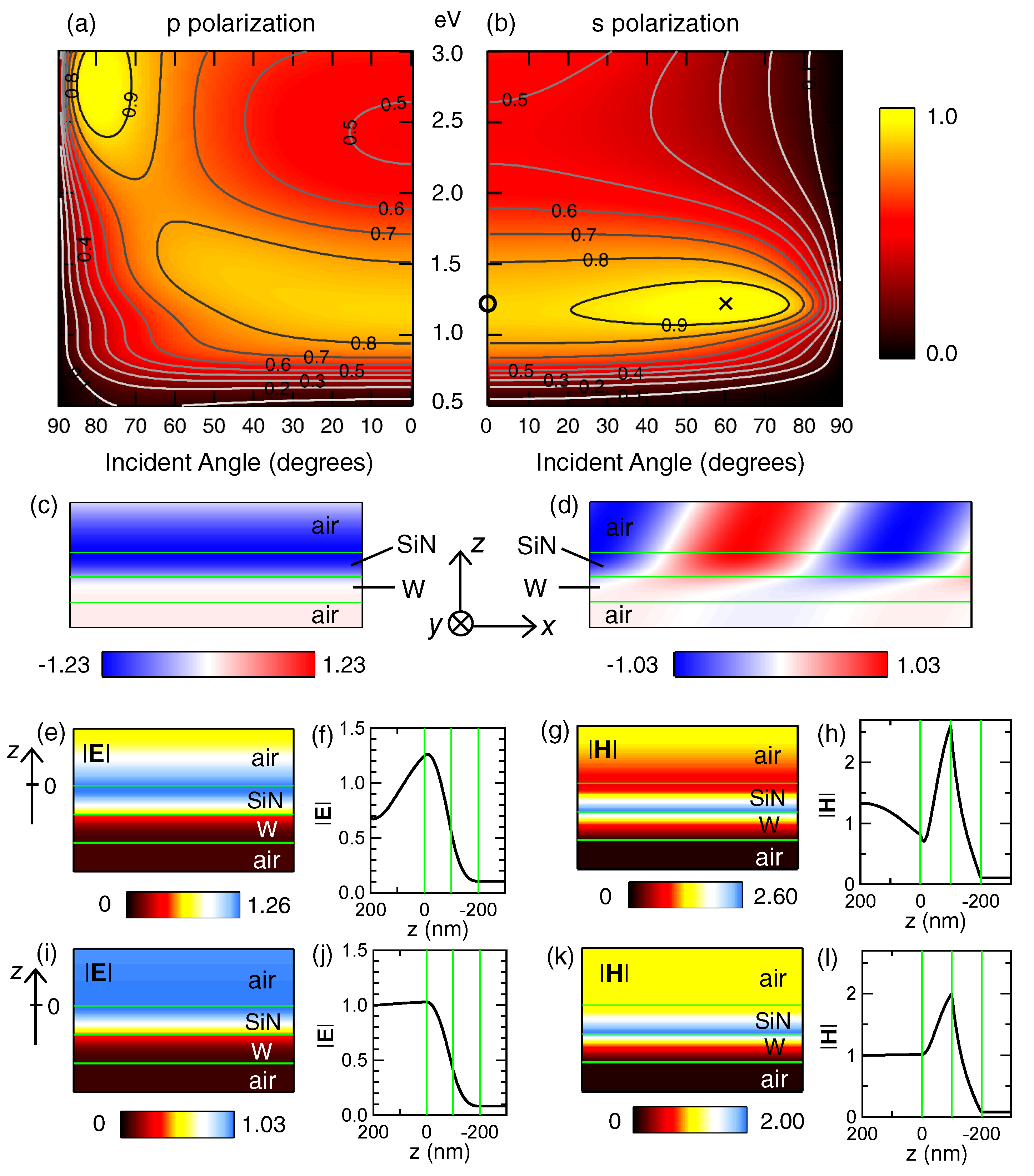
Figure 4.
(a,b) Absorptance spectra of 1D periodic W-SiN-W membranes under p and s polarizations, respectively. The schematic is given in Figure 1d. The incidence was set to be normal. Width of air slit, S, was varied from 150 to 850 nm, which is symbolized as S150 to S850, respectively, while the periodicity was fixed at 1000 nm. The color usage is in common with (a,b).

Figure 5.
EM-field distributions of the 1D W-SiN-W membrane of S550 in Figure 4. (a,b) absolute values of electric- and magnetic-field distributions, and , respectively; the incident polarization and wavelength are indicated by the sky-blue cone in Figure 4a; (c,d) and distributions, respectively; the incidence condition is indicated by the sky-blue cone in Figure 4b. The green lines commonly represent the boundaries of the 1D W-SiN-W structure. The coordinate axes are shown, in common, at the left-hand side. All the panels are shown in linear scale in the minimum-to-maximum manners.
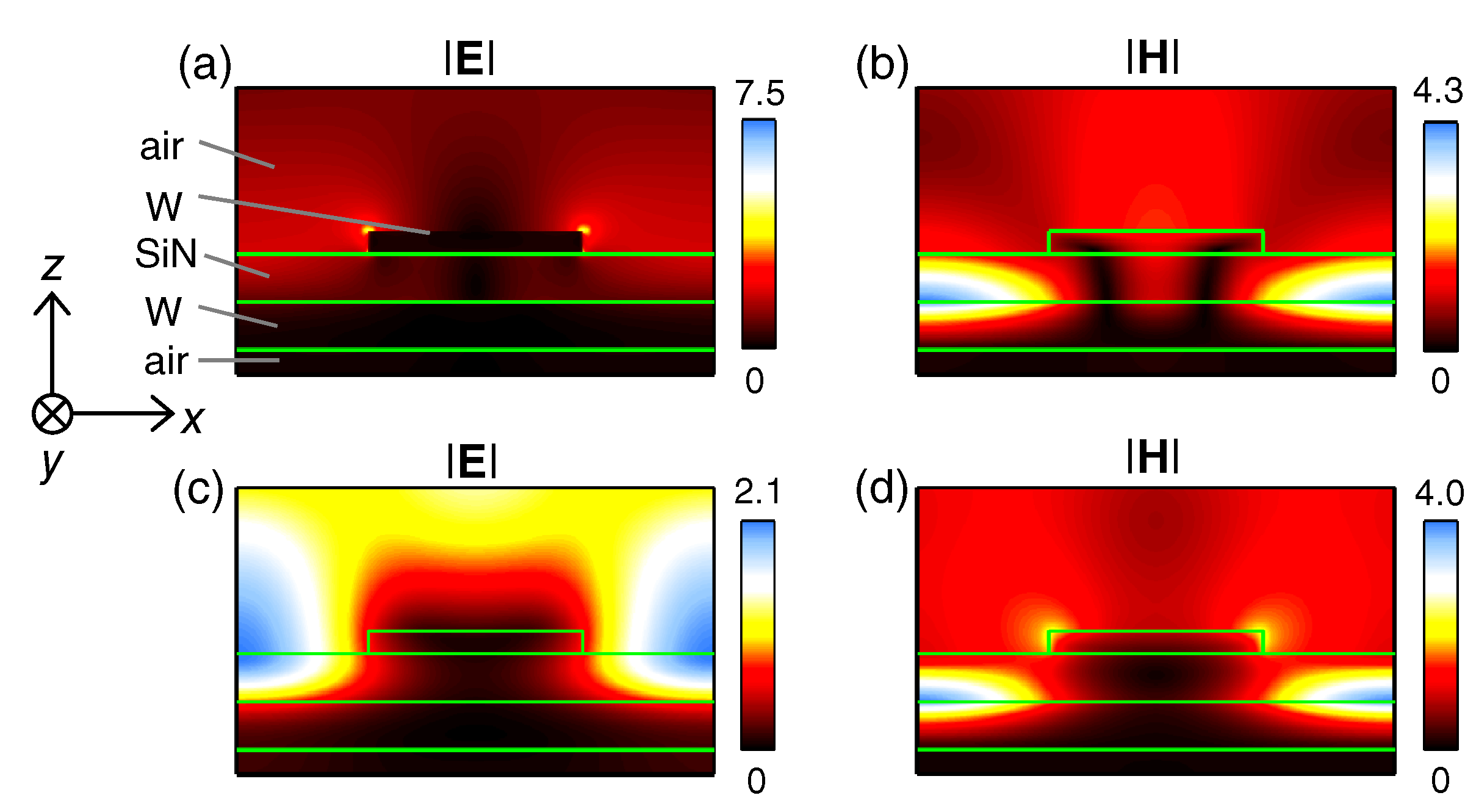
Figure 6.
EM-field distributions of the 1D W-SiN-W membrane of S750 in Figure 4. (a,b) and distributions, respectively; the p-polarized incidence condition is indicated by the red cone with the mark 6a in Figure 4a; (c,d) and distributions, respectively; the p-polarized incidence corresponds to the longer wavelength peak in Figure 4a, indicated by the red cone with the mark 6c. (e,f) and distributions, respectively; the s-polarized incidence condition is indicated in Figure 4b with the red cone with the mark 6e. The green lines commonly represent the boundaries of the 1D W-SiN-W structure. The coordinate axes are shown in common. All the panels are shown in linear scale in the minimum-to-maximum manners.

Figure 7.
Absorptance spectra of 2D periodic W-SiN-W membranes at the normal incidence. (a,b) on-top rectangular (side nm) and circular patches (diameter nm), whose schematics are illustrated in Figure 1e,f, respectively. The black and green curves denote the 2D membranes of SiN thickness (t) 100 and 200 nm, respectively. The periodicity P was set to nm in these cases.

Figure 8.
EM-field distributions of the 2D W-SiN-W membrane at the perfect-absorption condition indicated by the black cone in Figure 7a. (a,b) the xz-section views of and distributions, respectively. The xz section cuts through the center of the rectangular W patch; (c,d) the yz-section views, corresponding to (a,b), respectively; (e,f) the xy-section views of and distributions, respectively. The z positions are indicated by the cones in (a–d), respectively. The green lines represent the boundaries of the 2D periodic W-SiN-W structure. The relevant coordinate axes are shown on the left-hand side. All of the panels are shown in linear scale in the minimum-to-maximum-value manners.

© 2017 by the author. Licensee MDPI, Basel, Switzerland. This article is an open access article distributed under the terms and conditions of the Creative Commons Attribution (CC BY) license (http://creativecommons.org/licenses/by/4.0/).
Share and Cite
MDPI and ACS Style
Iwanaga, M. Perfect Light Absorbers Made of Tungsten-Ceramic Membranes. Appl. Sci. 2017, 7, 458. https://doi.org/10.3390/app7050458
AMA Style
Iwanaga M. Perfect Light Absorbers Made of Tungsten-Ceramic Membranes. Applied Sciences. 2017; 7(5):458. https://doi.org/10.3390/app7050458
Chicago/Turabian StyleIwanaga, Masanobu. 2017. "Perfect Light Absorbers Made of Tungsten-Ceramic Membranes" Applied Sciences 7, no. 5: 458. https://doi.org/10.3390/app7050458
Note that from the first issue of 2016, this journal uses article numbers instead of page numbers. See further details here.