
A Substrate-Reclamation Technology for GaN-Based Lighting-Emitting Diodes Wafer

1
Department of Industrial Engineering and Management, Da-Yeh University, Changhua 51591, Taiwan
2
Department of Materials Science and Engineering, National Chung Hsing University, Taichung 40227, Taiwan
*
Author to whom correspondence should be addressed.
Appl. Sci. 2017, 7(4), 325; https://doi.org/10.3390/app7040325
Submission received: 20 February 2017
/
Revised: 22 March 2017
/
Accepted: 23 March 2017
/
Published: 27 March 2017
Abstract
:This study reports on the use of a substrate-reclamation technology for a gallium nitride (GaN)-based lighting-emitting diode (LED) wafer. There are many ways to reclaim sapphire substrates of scrap LED wafers. Compared with a common substrate-reclamation method based on chemical mechanical polishing, this research technology exhibits simple process procedures, without impairing the surface morphology and thickness of the sapphire substrate, as well as the capability of an almost unlimited reclamation cycle. The optical performances of LEDs on non-reclaimed and reclaimed substrates were consistent for 28.37 and 27.69 mcd, respectively.
1. Introduction
Gallium nitride (GaN) is a direct-bandgap semiconductor. It is commonly used for fabricating light-emitting diodes (LEDs) due to their wide bandgap, chemical stability, and high temperature stability. These LEDs emit from the ultraviolet to the visible range [1,2,3]. Sapphire (Al2O3) has become a key material for fabricating GaN-based LEDs because it serves as an excellent epitaxial substrate due to its small lattice-constant mismatch with GaN. In particular, patterned sapphire substrates (PSSs) constitute an important epitaxial substrate for GaN-based LEDs because they enhance the light-extraction efficiency and internal quantum efficiency of LEDs [4,5,6]. The price of a 4 in PSS is approximately $30–32 USD [7], so PSSs account for about 25% of the total cost of an LED chip. Thus, reclaiming the sapphire substrate for GaN-based LED wafers can significantly reduce the manufacturing cost of LED chips. A chemical mechanical polishing (CMP) method is currently used universally to reclaim substrates [8,9,10]. However, the disadvantages of CMP include process complexity, surface scrapes, and thinning of the sapphire substrate. Surface scrapes and thinning result in the performance failure of the epitaxial film. Moreover, CMP makes the PSS pattern disappear. In the present work, we study a substrate-reclamation technology to avoid these disadvantages. In a non-vacuum state, we prepare a reclaimed substrate by thermally decomposing a GaN epitaxial film in a furnace system. We also investigate the properties of decomposed GaN on PSSs and the regrown LED epilayers on the reclaimed PSS.
2. Experimental Section
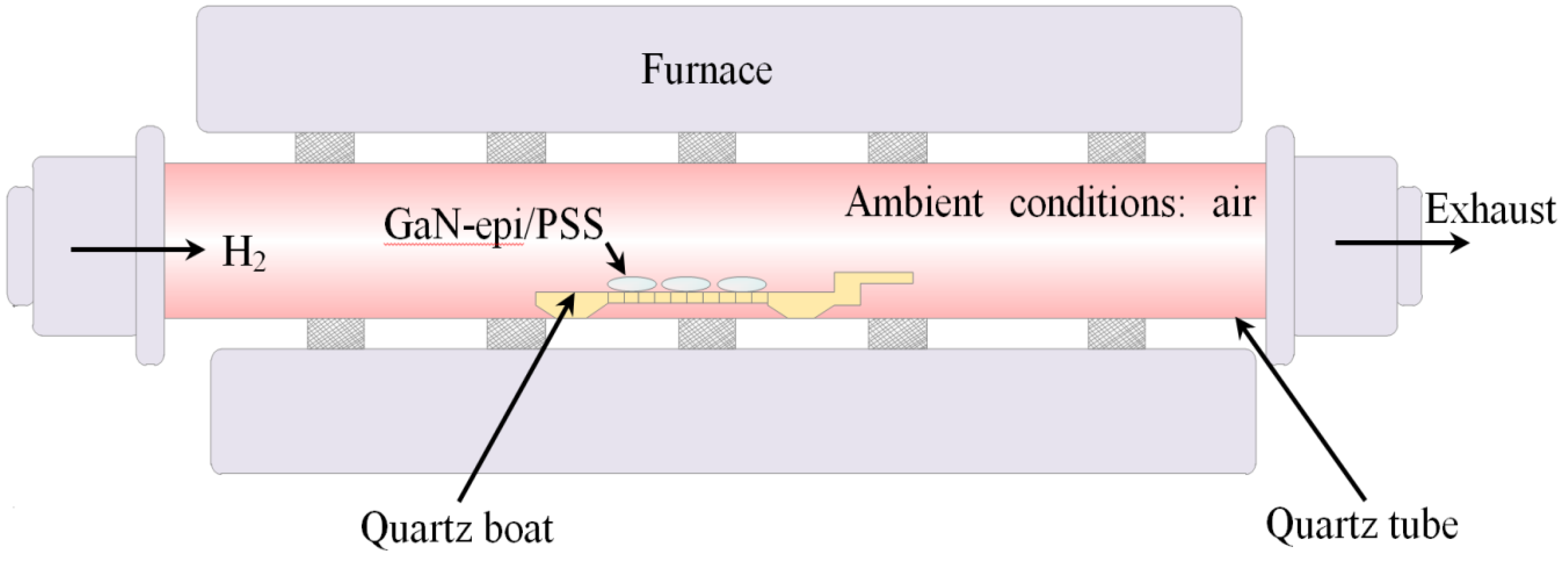
The sample consisted of GaN-based LED epilayers grown on a PSS (GaN-epi/PSS), which we fabricated by metalorganic chemical vapor deposition. For the PSS, the cone-pattern diameter, spacing, and height were 4, 2, and 1.4 μm, respectively. GaN-based LEDs epilayers (thickness = 3.5 μm) were produced by using standard epitaxial procedures. All samples involved similar epilayers and process procedures, except for the substrate reclaim conditions. The procedures involved in the substrate-reclaim process are as follows: The GaN-epi/PSS was loaded into a furnace, following which H2 was released into the furnace, as depicted in Figure 1. The process temperature, H2 flow rate, and process time for the GaN decomposition were varied in a non-vacuum state to determine the initial decomposition parameters. In process I, the GaN-epi/PSS is prepared at temperatures ranging from 800 to 1200 °C and at gas-flow rates of 10 sccm for 30 min. In process II, an operation temperature (1200 °C) is imposed on the GaN-epi/PSS according to the results of process I and the gas-flow rate is 25 sccm for 30, 60, and 90 min. The details of the substrate-reclaim conditions are given in Table 1. The sample is then unloaded and the reaction products on the sample surface are removed by using an alkaline solution to form an exposed PSS. Here the exposed PSS is defined to be reclaimed PSS. Following, GaN-based LEDs epilayers are regrown on reclaimed PSS, and a 10 × 24 mil2 chip is fabricated. This type of LED is called “LED/reclaimed PSS”. The procedure for fabricating chip devices in this study is as follows: An indium tin oxide transparent conductive layer and Cr/Au metal were deposited on the p- and n-type GaN as Ohmic contacts, respectively. Finally, to confirm the properties of the LED/reclaimed PSS device, GaN-based LED epilayers grown on a non-reclaimed PSS were also fabricated. Here, “LED/non-reclaimed PSS” denotes this type of LED.
3. Results and Discussion
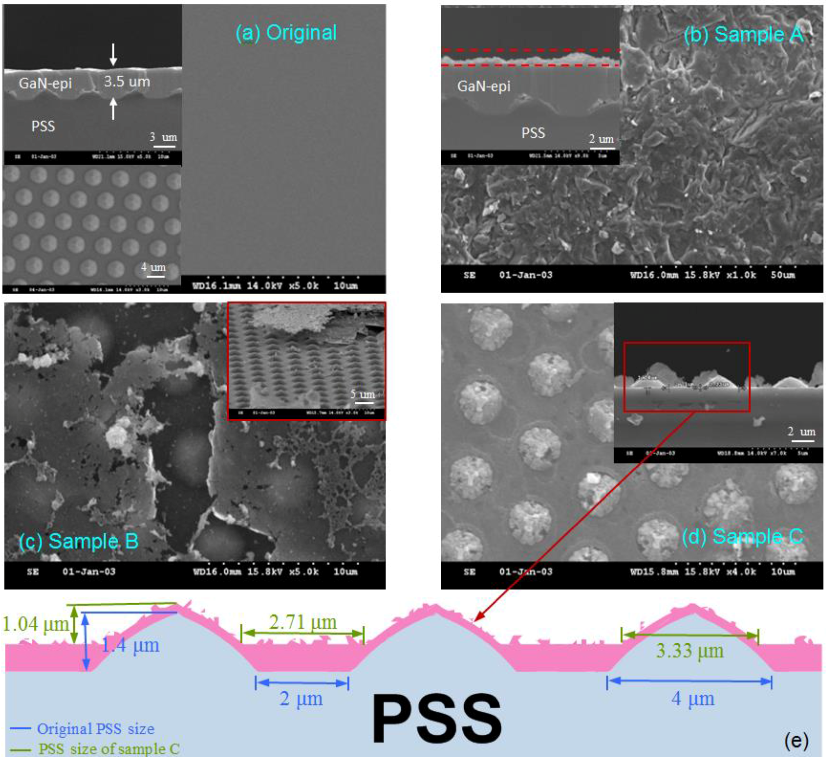
Figure 2 shows top-view and cross-section scanning electron microscope (SEM) images of GaN-epi/PSSs both exposed and not exposed to gas-flow rates of 10 sccm for 30 min and at various temperatures (800–1200 °C). Figure 2a shows the surface morphology and cross-section of the GaN-epi/PSSs (i.e., original samples). In addition, the top-view SEM image of the original pristine sapphire substrate is also shown in the inset of Figure 2a. Preparing the GaN-epi/PSSs at 800 °C changed the surface morphology of the GaN-epi film, as shown in Figure 2b. Upon increasing the process temperature to 1000 °C, sheet-shape decomposition began in the GaN epilayers and the substrate cone patterns started to exposed, as shown in Figure 2c. Further increasing the temperature to 1200 °C resulted in cone patterns appearing over the entire sample surface. Figure 2d,e show the top view and cross-section and an enlarged schematic of the PSS after being exposed to a gas-flow rate of 10 sccm for 30 min at 1200 °C. The PSS cone diameter, spacing, and height were 3.33, 2.71, and 1.04 μm, respectively. By comparing them with the original cone pattern, these results indicate that the GaN-epi film still did not completely decompose under these process conditions. In addition, the GaN-epi decomposition reaction correlated positively with the process temperature, which is consistent with the results of Schmid-Fetzer et al. [11].
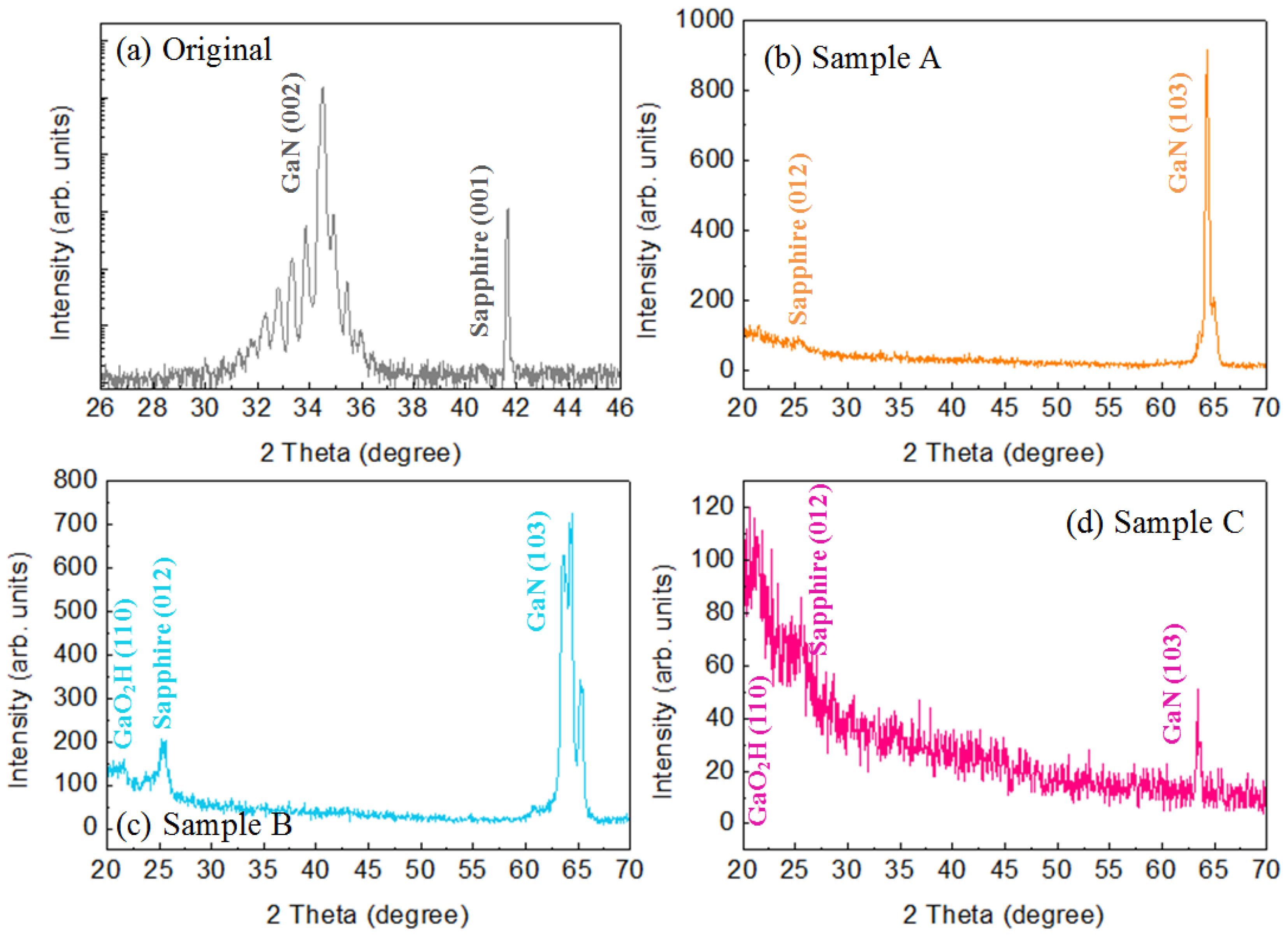
Figure 3 shows the X-ray diffraction (XRD) spectra of the GaN-epi/PSS prepared and not prepared according to substrate-reclamation process I. The diffraction pattern from untreated GaN-epi/PSS has a sharp GaN (002) peak near 34.6°, several satellite peaks from the InGaN/GaN active layers, and a sapphire (001) peak near 2θ = 41.6°, as shown in Figure 3a. The grazing-angle XRD spectra of samples A, B, and C appear in Figure 3b–d, respectively. The diffraction peaks from the GaN (103) phase near 2θ = 63.6° gradually began to weaken with increasing the temperature from 800–1200 °C. Moreover, when the operation temperature exceeded 1000 °C, a GaO2H (110) peak near 2θ = 21.47° appeared in the diffraction pattern. These results indicate that the GaN-epi film on the PSS begins to transform and to produce a GaO2H derivative. Note that the GaN-epi film still exists under the conditions of process I. Figure 4 shows the grazing-angle XRD spectra of the GaN-epi/PSS prepared using substrate-reclamation process II. The diffraction pattern reveals a GaO2H (110) peak at 2θ ≅ 21.47° and a sapphire (012) peak at 2θ ≅ 25.65°. As the process time increased from 30 min to above 60 min, the diffraction peaks of the sapphire (113) phase appeared near 43.47°. Comparing these results with those shown in Figure 3 shows that no GaN peak appeared in the GaN-epi/PSS XRD pattern under the conditions of process II. The results indicate that the decomposition reaction of the GaN-epi film on the PSS is increased when the gas-flow rate increases from 10 to 25 sccm, which is consistent with the results of Koleske et al. [12]. Moreover, the exposed pattern morphology is more notable with increasing the process time under a gas-flow rate of 25 sccm, as shown in the SEM image in the inset of Figure 4.
To ensure the pure surface of the exposed PSS, we analyzed the photoelectron spectrum of the GaN-epi/PSS prepared with a gas-flow rate of 25 sccm for 90 min followed by wet etching (see Figure 5). These results show the Al2p, Al2s, O2s, and O1s peaks located near 74.4, 118, 23, and 531 eV, respectively. The binding energy of O and Al corresponds to that of O and Al in Al2O3 (i.e., the sapphire substrate) [13,14]. This result is consistent with an exposed PSS surface without Ga and demonstrates that no GaO2H is present at the surfaces of the exposed PSS. The C1s peaks are due to the C element adsorbed on the sample surface from the atmosphere ambient. The SEM image in Figure 5 indicates that exposure to a gas-flow rate of 25 sccm for 90 min followed by wet etching results in a pure PSS surface. Figure 6 shows the optical and electrical performances for both LED types with an injection current of 20 mA. The light intensity for the LEDs/non-reclaimed PSS and LED/reclaimed PSS was 28.37 and 27.69 mcd, respectively. The forward voltage for the LED/non-reclaimed PSS and for the LED/reclaimed PSS was 3.16 and 3.18 V, respectively. These results reveal that both types of LEDs have similar optical and electrical characteristics, which indicates that sapphire substrates may be successfully re-used in epi-regrowth of GaN-based LEDs.
4. Conclusions
We have demonstrated that a substrate-reclamation technology allows us to achieve a reclamation cycle that is almost unlimited. This technology will help reduce the manufacturing cost of both chips and stock numbers of the scrap wafer in the LED industry. In this research, a GaN-epi/PSS was found that has a GaO2H (110) reactant on the surface of an exposed PSS and a GaN-epi film was completely dissociated after gas-flow rates of 25 sccm for 90 min at 1200 °C. The GaO2H (110) reactant was removed to form a pure exposed PSS using an alkaline solution and then the GaN-based LED epilayers were re-grown on reclaimed substrates successfully.
Acknowledgments
This study is supported by the National Science Council of the Republic of China under contract No. NSC-101-2218-E-212-001.
Author Contributions
Shih-Yung Huang conceived and designed the experimental procedures; Po-Jung Lin contributed the sample measurement results. All authors read and approved the final version of the manuscript to be submitted.
Conflicts of Interest
The authors declare no conflict of interest.
References
- Muramoto, Y.; Kimura, M.; Nouda, S. Development and future of ultraviolet light-emitting diodes: UV-LED will replace the UV lamp. Semicond. Sci. Technol. 2014, 29, 084004. [Google Scholar] [CrossRef]
- Park, J.; Sin, Y.G.; Kim, J.H.; Kim, J. Dependence of adhesion strength between GaN LEDs and sapphire substrate on power density of UV laser irradiation. Appl. Surf. Sci. 2016, 384, 353–359. [Google Scholar] [CrossRef]
- Vishwakarma, A.L.; Jayasimhadri, M. Significant enhancement in photoluminescent properties via flux assisted Eu3+ doped BaNb2O6 phosphor for white LEDs. J. Alloys Compd. 2016, 683, 379–386. [Google Scholar] [CrossRef]
- Han, M.; Han, N.; Jung, E.; Ryu, B.D.; Ko, K.B.; Cuong, T.V.; Kim, H.; Kim, J.K.; Hong, C.H. Effect of curved graphene oxide in a GaN light-emitting-diode for improving heat dissipation with a patterned sapphire substrate. Semicond. Sci. Technol. 2016, 31, 085010. [Google Scholar] [CrossRef]
- Lee, F.W.; Ke, W.C.; Cheng, C.H.; Liao, B.W.; Chen, W.K. Influence of different aspect ratios on the structural and electrical properties of GaN thin films grown on nanoscale-patterned sapphire substrates. Appl. Surf. Sci. 2016, 375, 223–229. [Google Scholar] [CrossRef]
- Shang, L.; Zhai, G.M.; Mei, F.H.; Jia, W.; Yu, C.Y.; Liu, X.G.; Xu, B.S. The effect of nucleation layer thickness on the structural evolution and crystal quality of bulk GaN grown by a two-step process on cone-patterned sapphire substrate. J. Cryst. Growth 2016, 442, 89–94. [Google Scholar] [CrossRef]
- Global Sapphire and LED Chip Market Report. Available online: http://www.ledinside.com/newsletter/1568 (accessed on 30 June 2016).
- Zhang, Z.F.; Liu, W.L.; Song, Z.T.; Hu, X.K. Two-Step Chemical Mechanical Polishing of Sapphire Substrate. J. Electrochem. 2010, 157, H688–H691. [Google Scholar] [CrossRef]
- Yan, W.X.; Zhang, Z.F.; Guo, X.H.; Liu, W.L.; Song, Z.T. The Effect of pH on Sapphire Chemical Mechanical Polishing. ECS J. Solid State Sci. Technol. 2015, 4, P108–P111. [Google Scholar] [CrossRef]
- Zhang, Y.; Lin, B.; Li, Z.C. An Overview of Recent Advances in Chemical Mechanical Polishing (CMP) of Sapphire Substrates. ECS Trans. 2013, 52, 495–500. [Google Scholar] [CrossRef]
- Unland, J.; Onderka, B.; Davydov, A.; Schmid-Fetzer, R. Thermodynamics and phase stability in the Ga-M system. J. Cryst. Growth 2003, 256, 33–51. [Google Scholar] [CrossRef]
- Koleske, D.D.; Wickenden, A.E.; Henry, R.L.; Culbertson, J.C.; Twigg, M.E. GaN decomposition in H2 and N2 at NOVPE temperatures and pressures. J. Cryst. Growth 2003, 33, 466–483. [Google Scholar]
- Fu, Q.; Wagner, T.; Ryhle, M. Hydroxylated a-Al2O3 (0001) surfaces and metal/a-Al2O3 (0001) interfaces. Surf. Sci. 2006, 600, 4870–4877. [Google Scholar] [CrossRef]
- Wagner, C.; Riggs, W.; Davis, L.; Moulder, J. Handbook of X-ray Photoelectron Spectroscopy; Perkin-Elmer Corporation: New York, NY, USA, 1979; pp. 54–55. [Google Scholar]
Figure 1.
Schematic diagram showing substrate-reclaim setup for GaN-epi/patterned sapphire substrate (PSS) by furnace process in H2 gas.
Figure 1.
Schematic diagram showing substrate-reclaim setup for GaN-epi/patterned sapphire substrate (PSS) by furnace process in H2 gas.

Figure 2.
Top-view and cross-section scanning electron microscope (SEM) micrographs of GaN-epi/PSSs prepared and not prepared according to substrate-reclamation process I. The enlarged schematic diagram of the PSS in panel (e) depicts the cone pattern size of sample C.
Figure 2.
Top-view and cross-section scanning electron microscope (SEM) micrographs of GaN-epi/PSSs prepared and not prepared according to substrate-reclamation process I. The enlarged schematic diagram of the PSS in panel (e) depicts the cone pattern size of sample C.

Figure 3.
X-ray diffraction (XRD) spectra of GaN-epi/PSS with and without using substrate-reclamation process I.
Figure 3.
X-ray diffraction (XRD) spectra of GaN-epi/PSS with and without using substrate-reclamation process I.

Figure 4.
XRD spectra of GaN-epi/PSSs prepared by using substrate-reclamation process II.
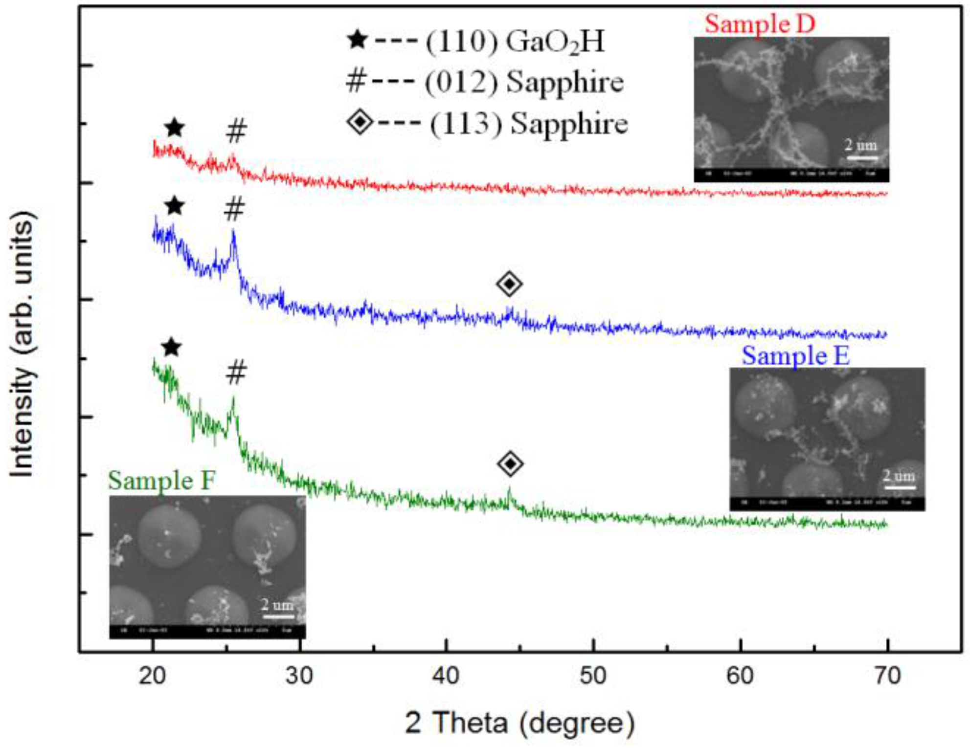
Figure 5.
Photoelectron spectrum of GaN-epi/PSS prepared with a gas-flow rate of 25 sccm for 90 min followed by wet etching.
Figure 5.
Photoelectron spectrum of GaN-epi/PSS prepared with a gas-flow rate of 25 sccm for 90 min followed by wet etching.
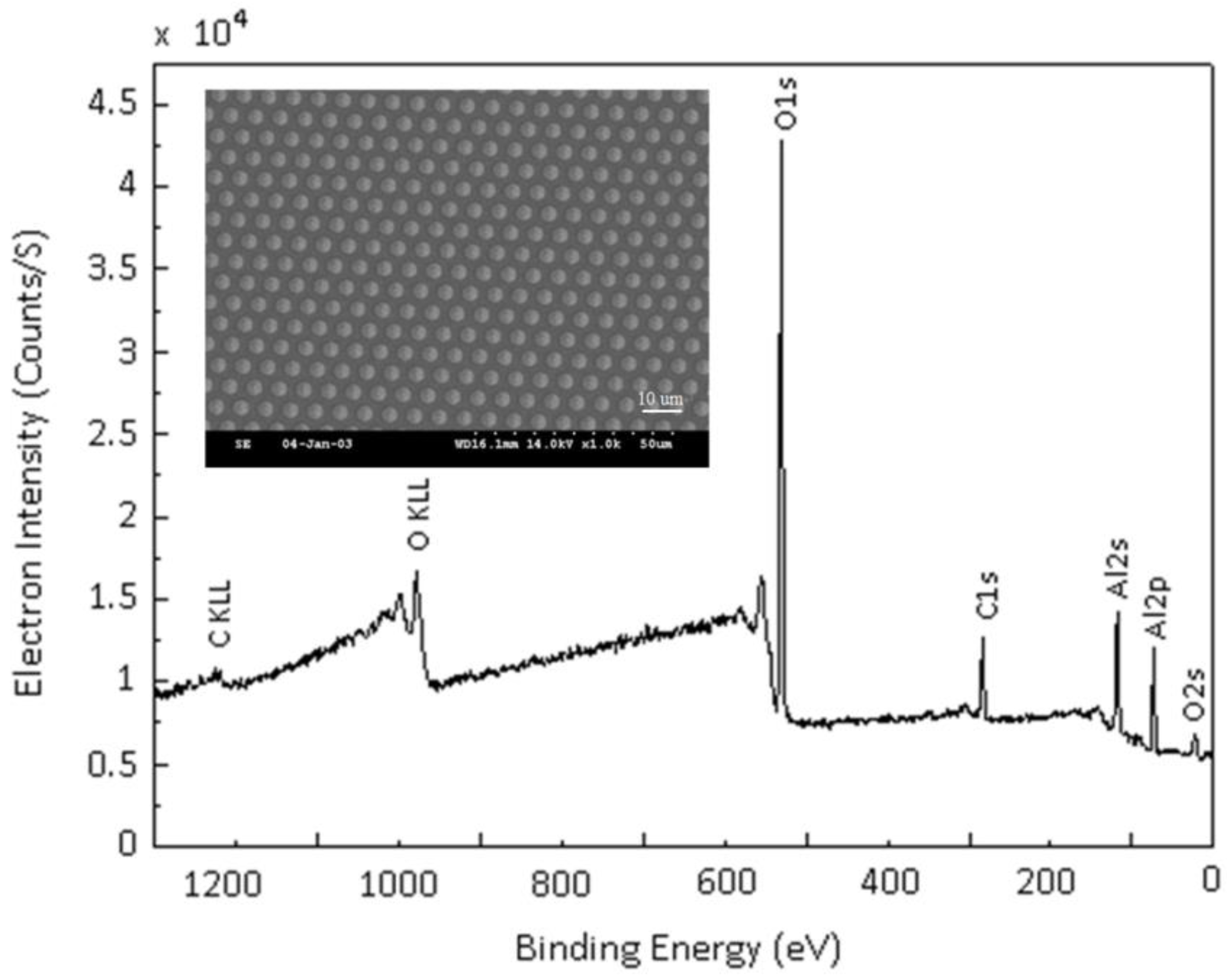
Figure 6.
(a) Optical and (b) electrical performance of both LED types with 20 mA injection current.
Figure 6.
(a) Optical and (b) electrical performance of both LED types with 20 mA injection current.


Table 1.
Substrate-reclaim conditions of GaN-epi/patterned sapphire substrate (PSS).
| Sample: GaN-epi/PSSs Experimental Conditions | Temperature/°C | Gas-Flow Rates/sccm | Times/min |
|---|---|---|---|
| I. Processes under different temperatures | |||
| Sample A | 800 | 10 | 30 |
| Sample B | 1000 | ||
| Sample C | 1200 | ||
| II. Processes under different times | |||
| Sample D | 1200 | 25 | 30 |
| Sample E | 60 | ||
| Sample F | 90 | ||
© 2017 by the authors. Licensee MDPI, Basel, Switzerland. This article is an open access article distributed under the terms and conditions of the Creative Commons Attribution (CC BY) license (http://creativecommons.org/licenses/by/4.0/).
Share and Cite
MDPI and ACS Style
Huang, S.-Y.; Lin, P.-J. A Substrate-Reclamation Technology for GaN-Based Lighting-Emitting Diodes Wafer. Appl. Sci. 2017, 7, 325. https://doi.org/10.3390/app7040325
AMA Style
Huang S-Y, Lin P-J. A Substrate-Reclamation Technology for GaN-Based Lighting-Emitting Diodes Wafer. Applied Sciences. 2017; 7(4):325. https://doi.org/10.3390/app7040325
Chicago/Turabian StyleHuang, Shih-Yung, and Po-Jung Lin. 2017. "A Substrate-Reclamation Technology for GaN-Based Lighting-Emitting Diodes Wafer" Applied Sciences 7, no. 4: 325. https://doi.org/10.3390/app7040325
Note that from the first issue of 2016, this journal uses article numbers instead of page numbers. See further details here.