
Metal-Insulator-Metal Single Electron Transistors with Tunnel Barriers Prepared by Atomic Layer Deposition

Abstract
:1. Introduction
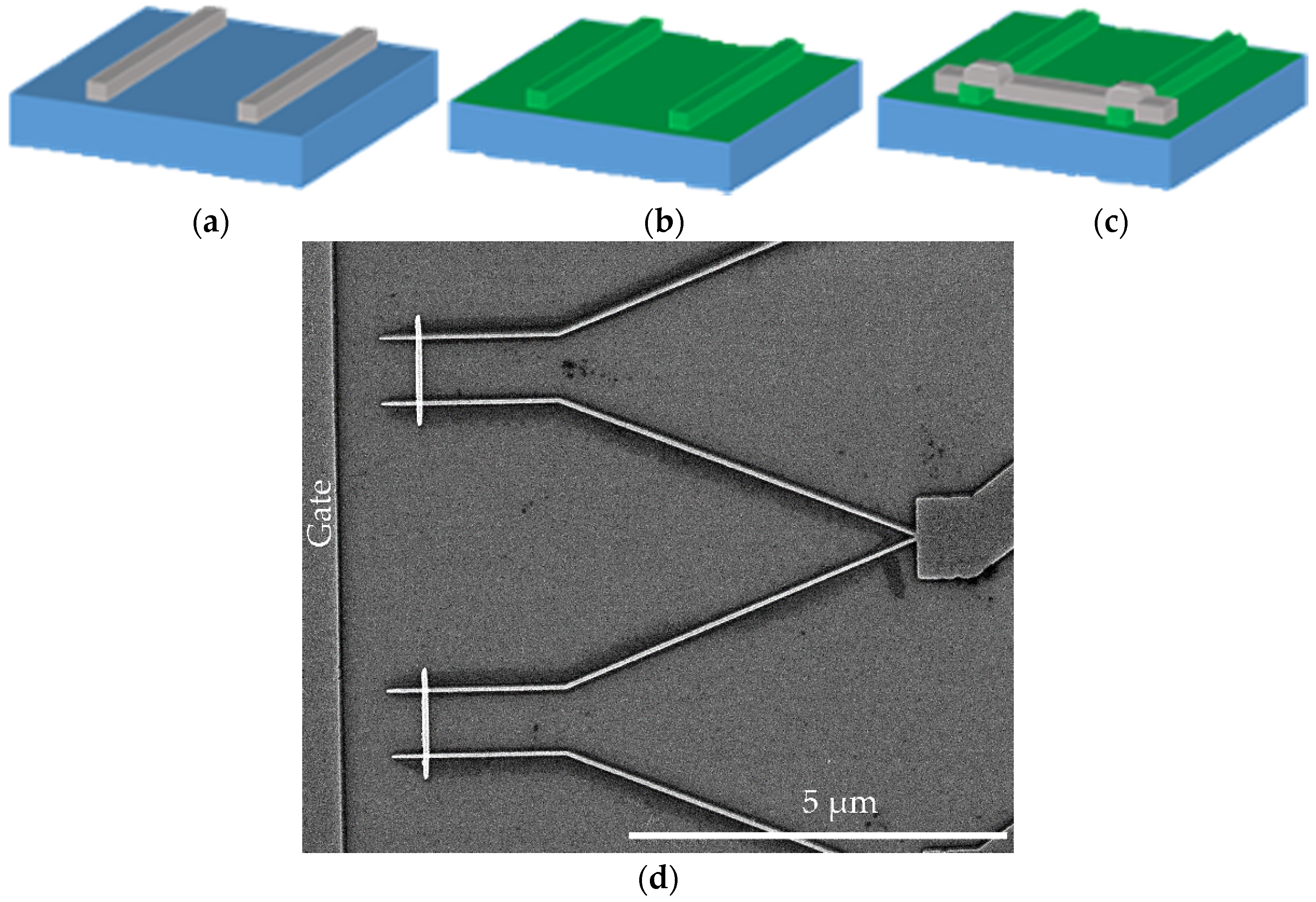
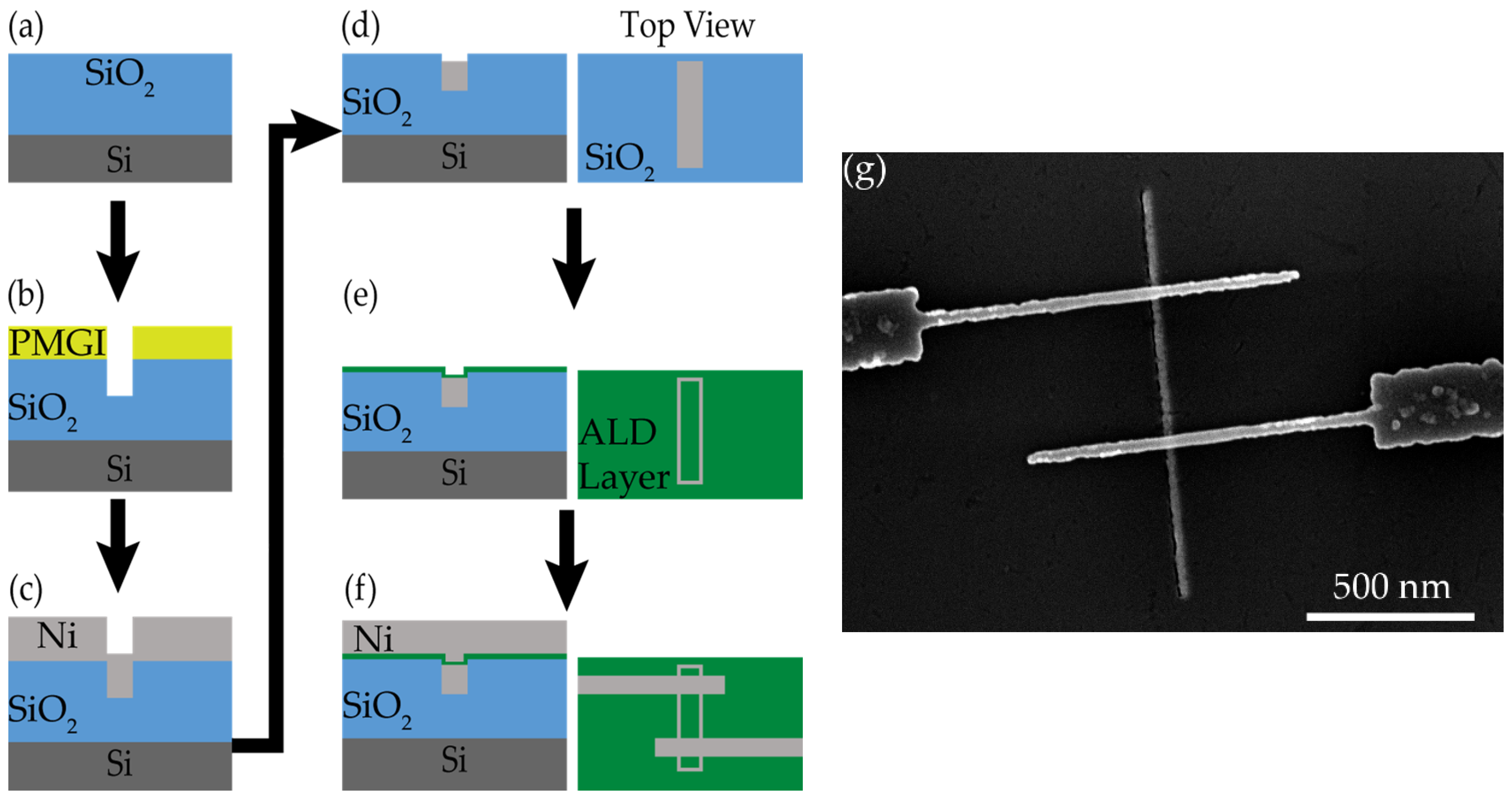
2. Materials and Methods
3. Results
3.1. Devices Featuring Pt-ALD Dielectric-Pt Junctions
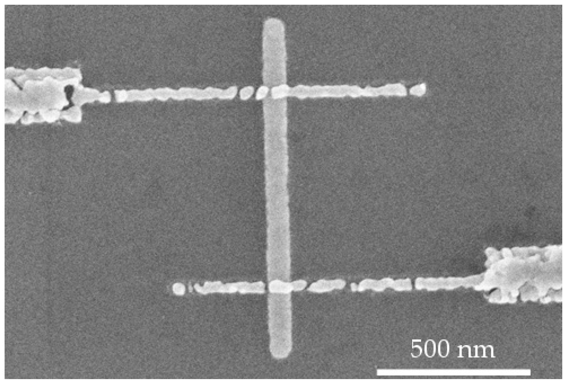
3.1.1. Initial Experiments: SETs with H2O-Based ALD of the Tunnel Barrier
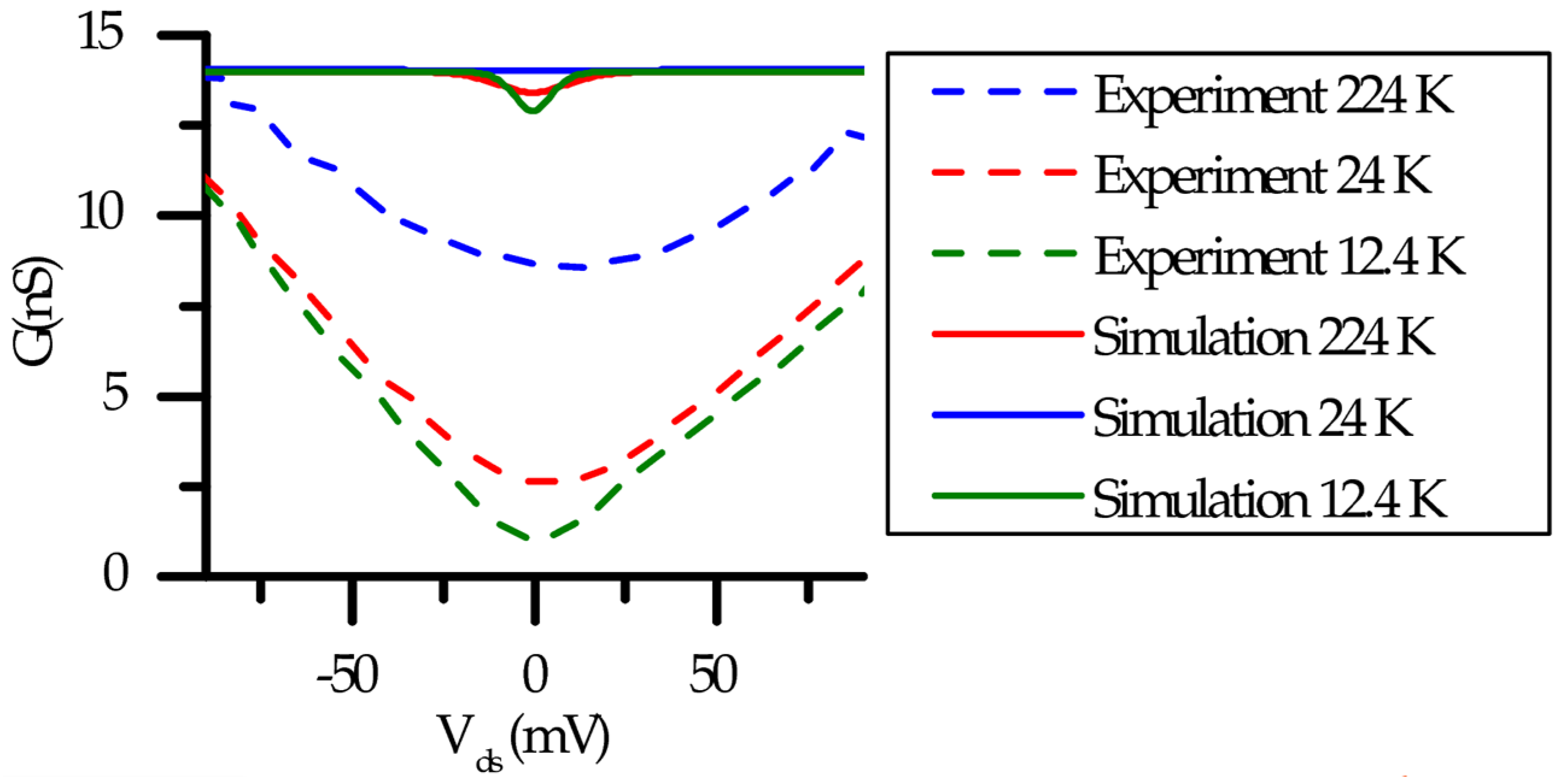
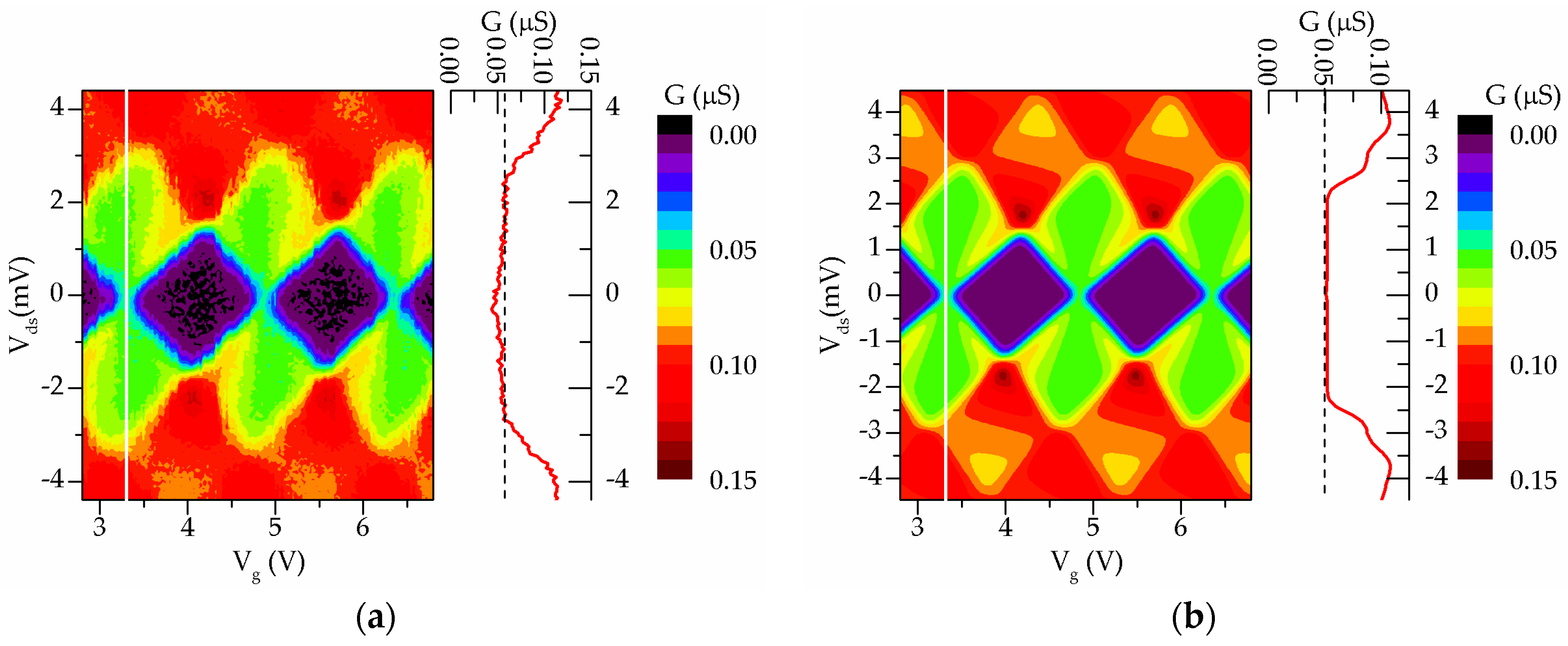
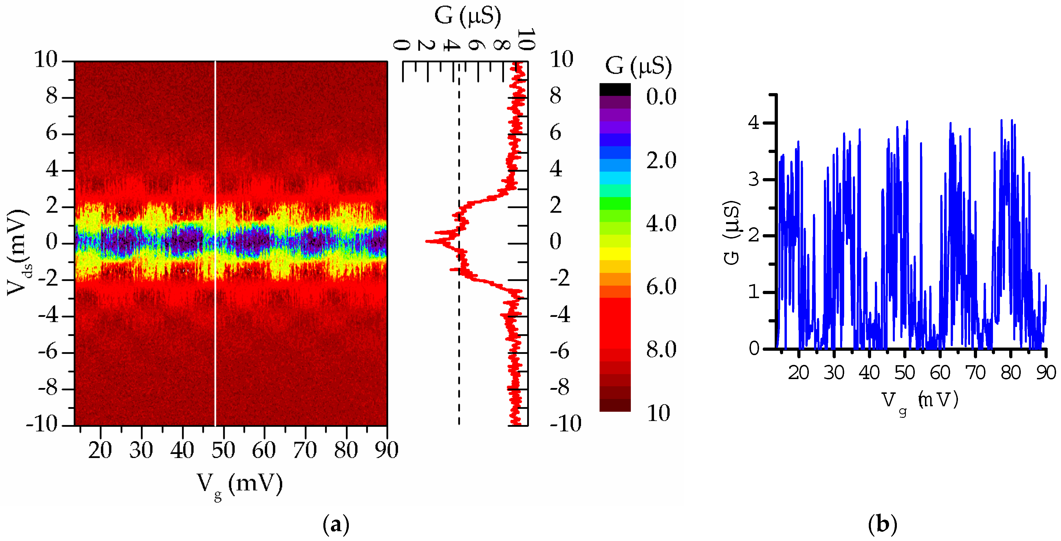
3.1.2. O3-Based vs. H2O-Based ALD of Al2O3 in SETs
3.2. Devices Featuring Ni-ALD Dielectric-Ni Junctions
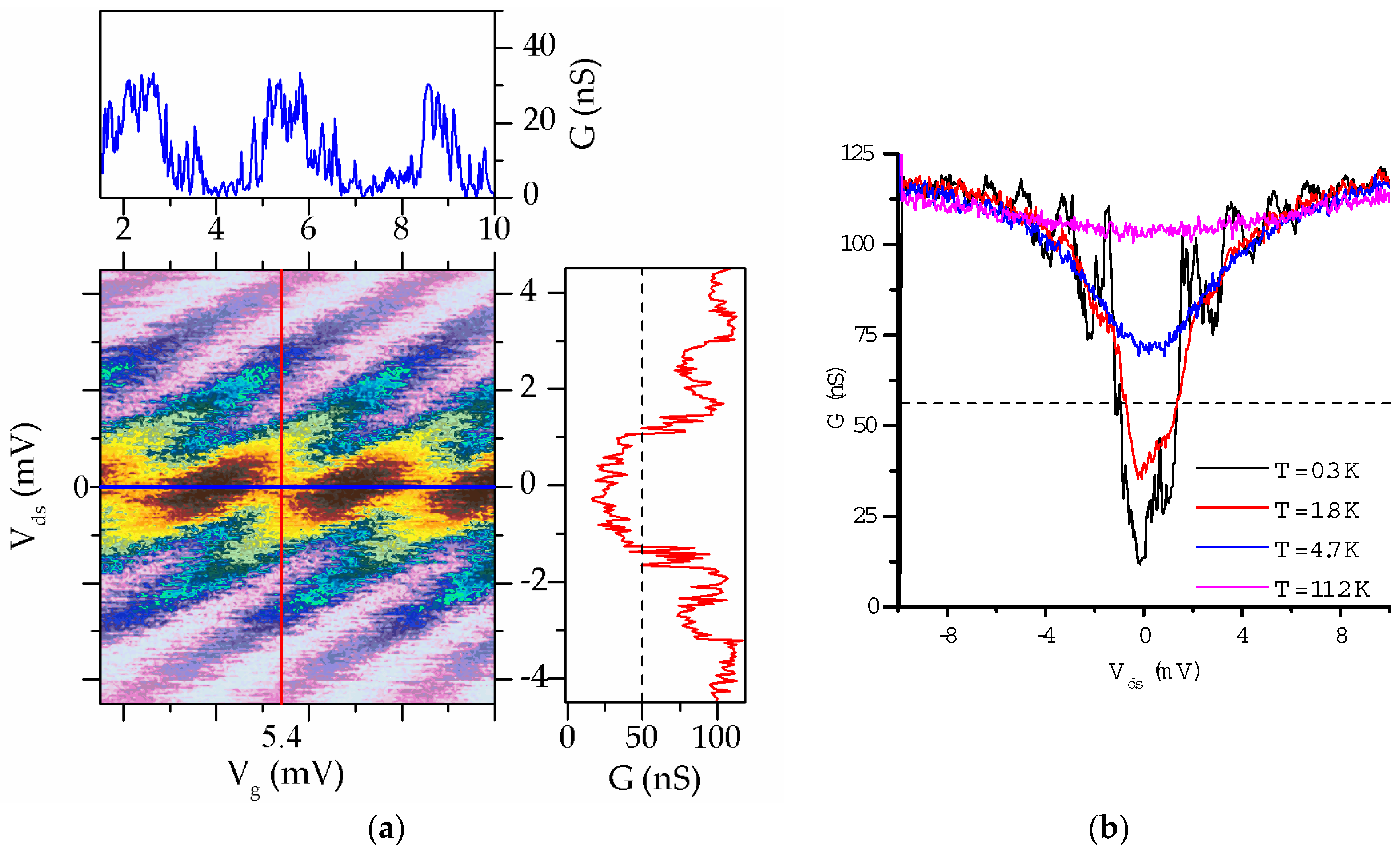
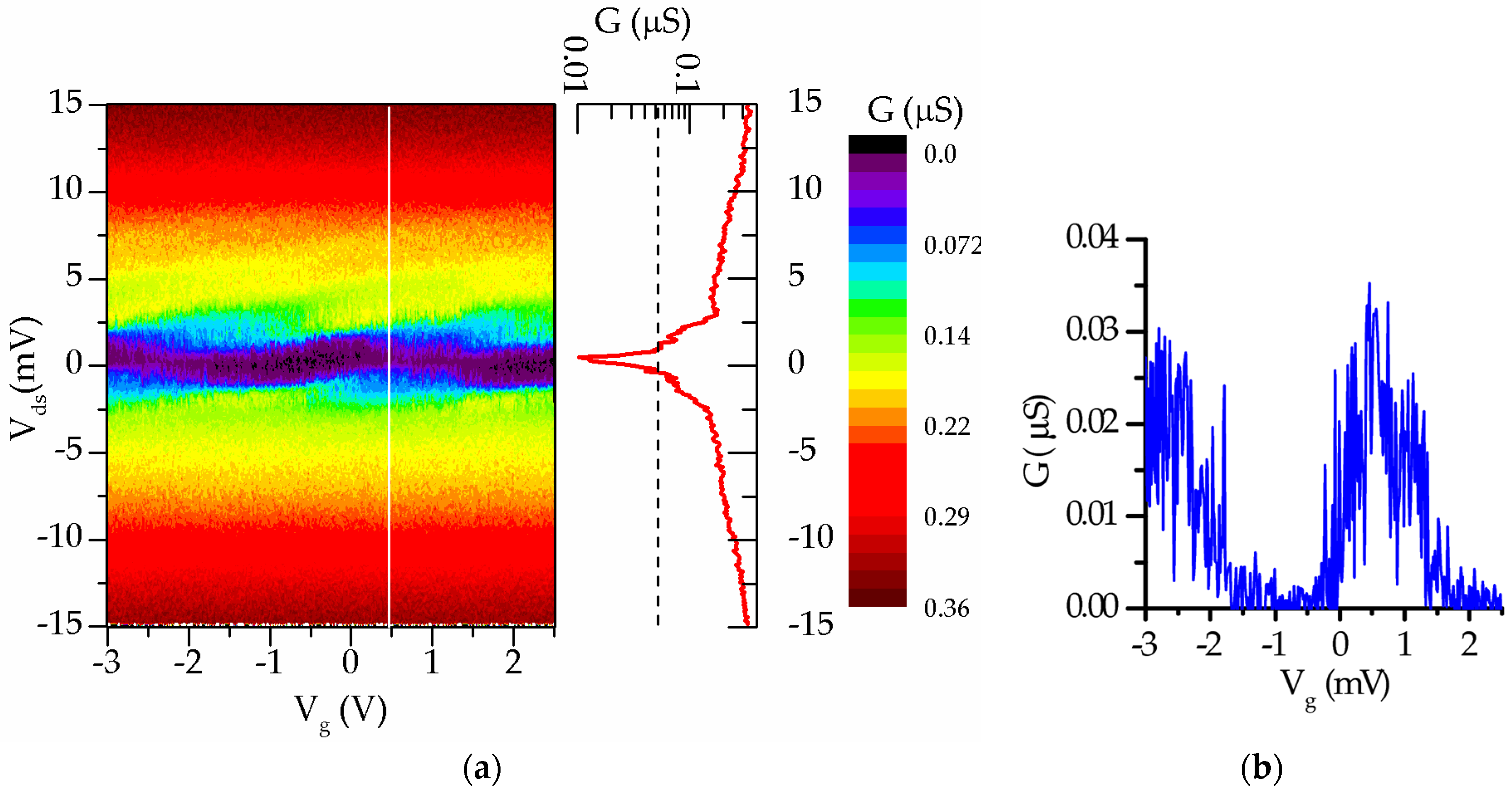
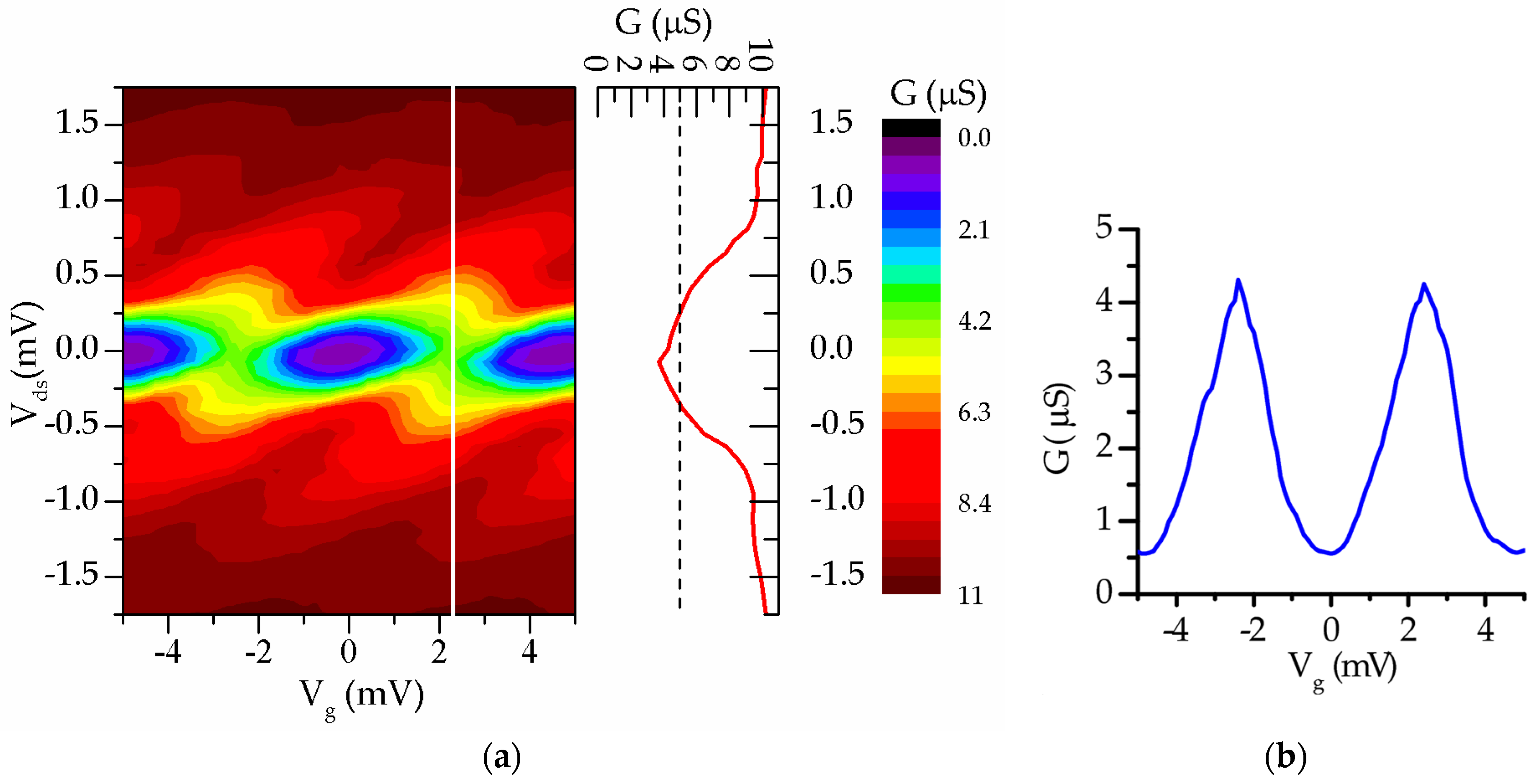
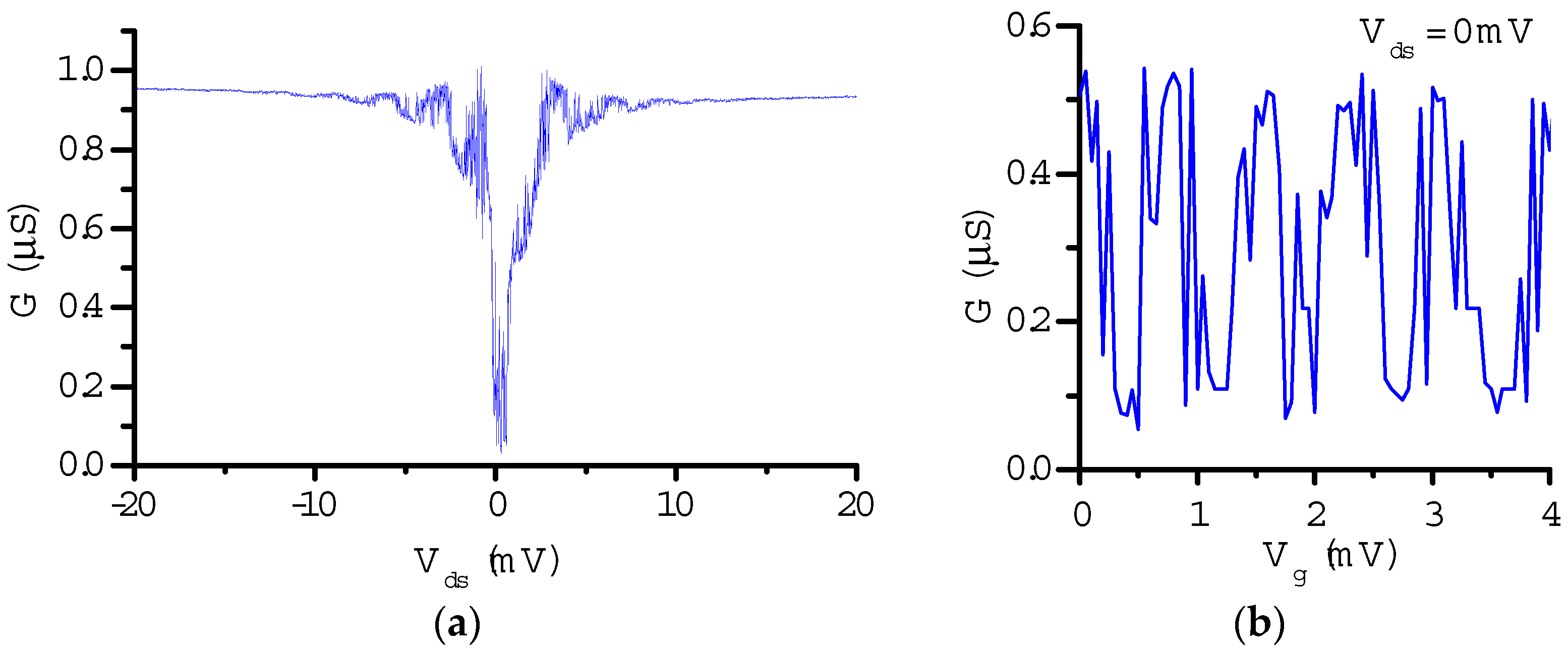
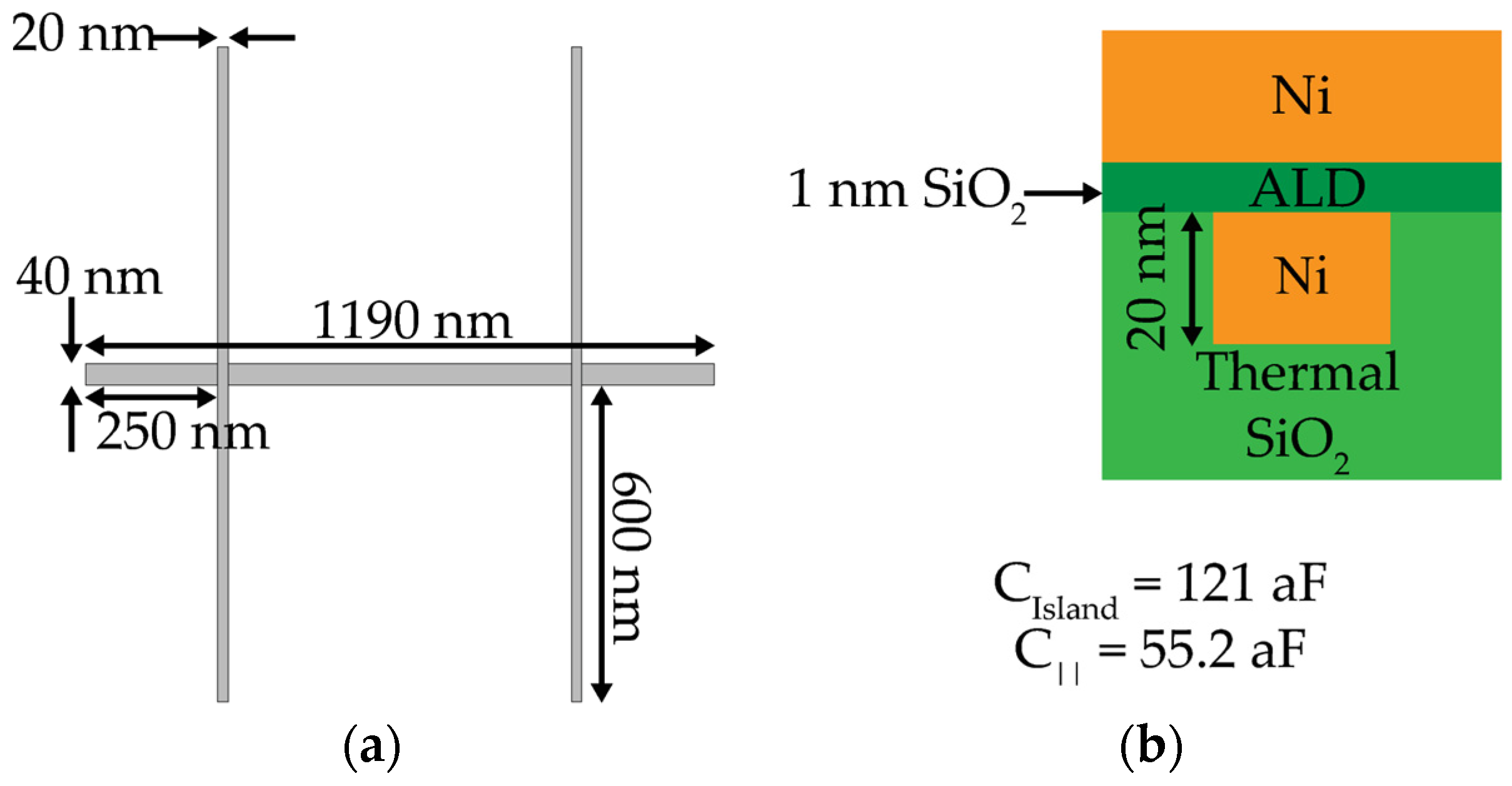
3.2.1. SET Devices with Ni-SiO2-Ni Tunnel Junctions
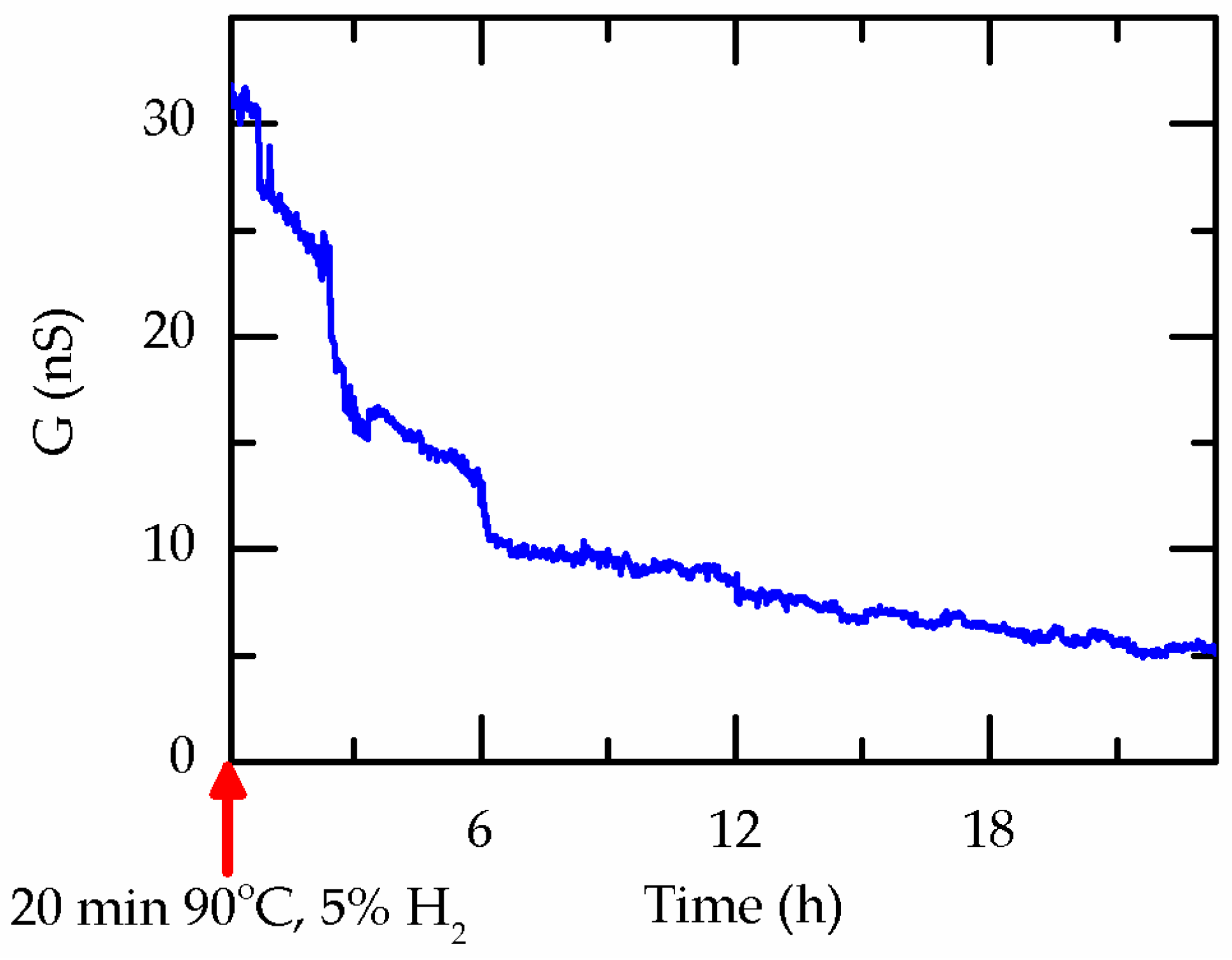
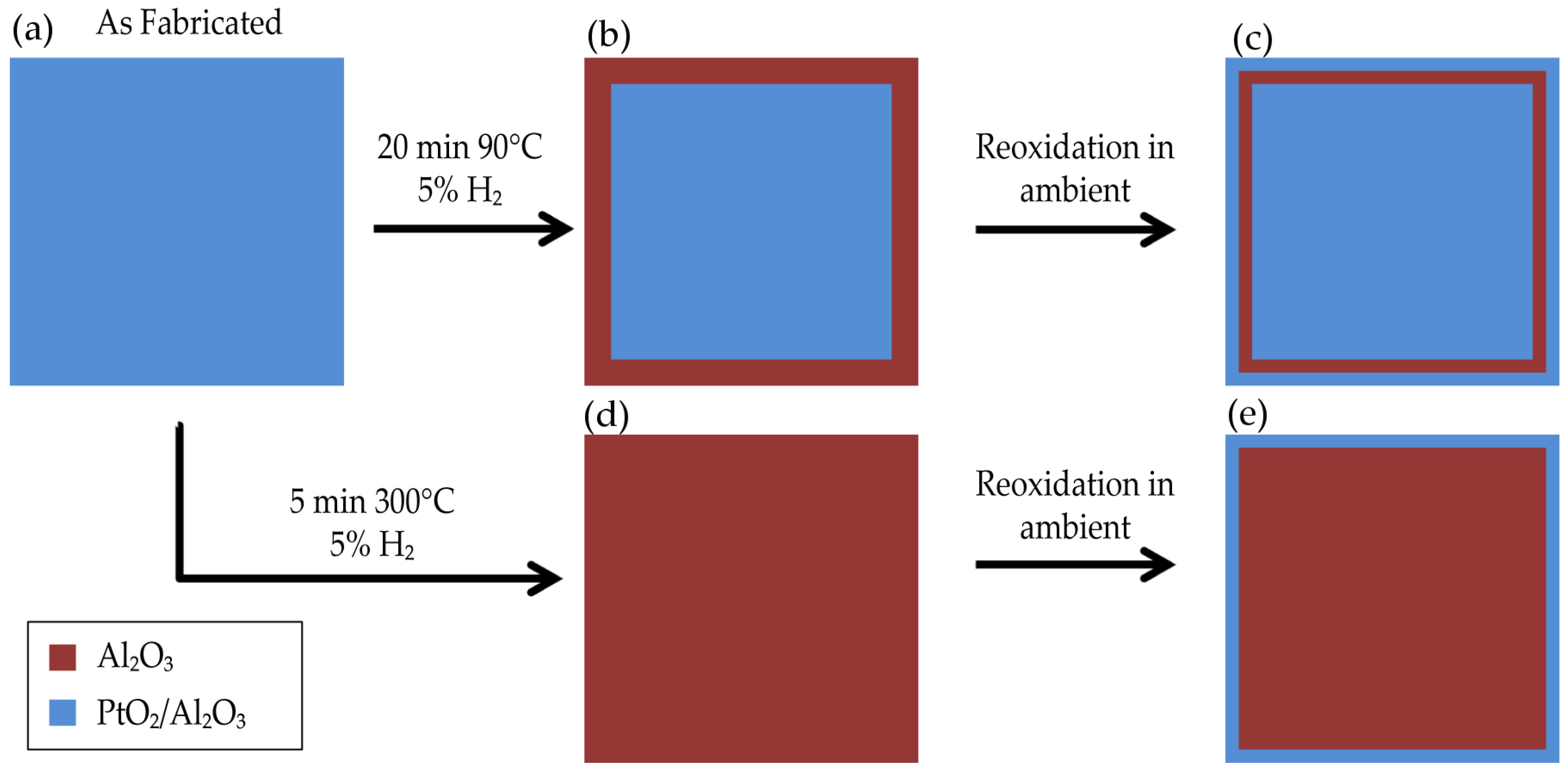
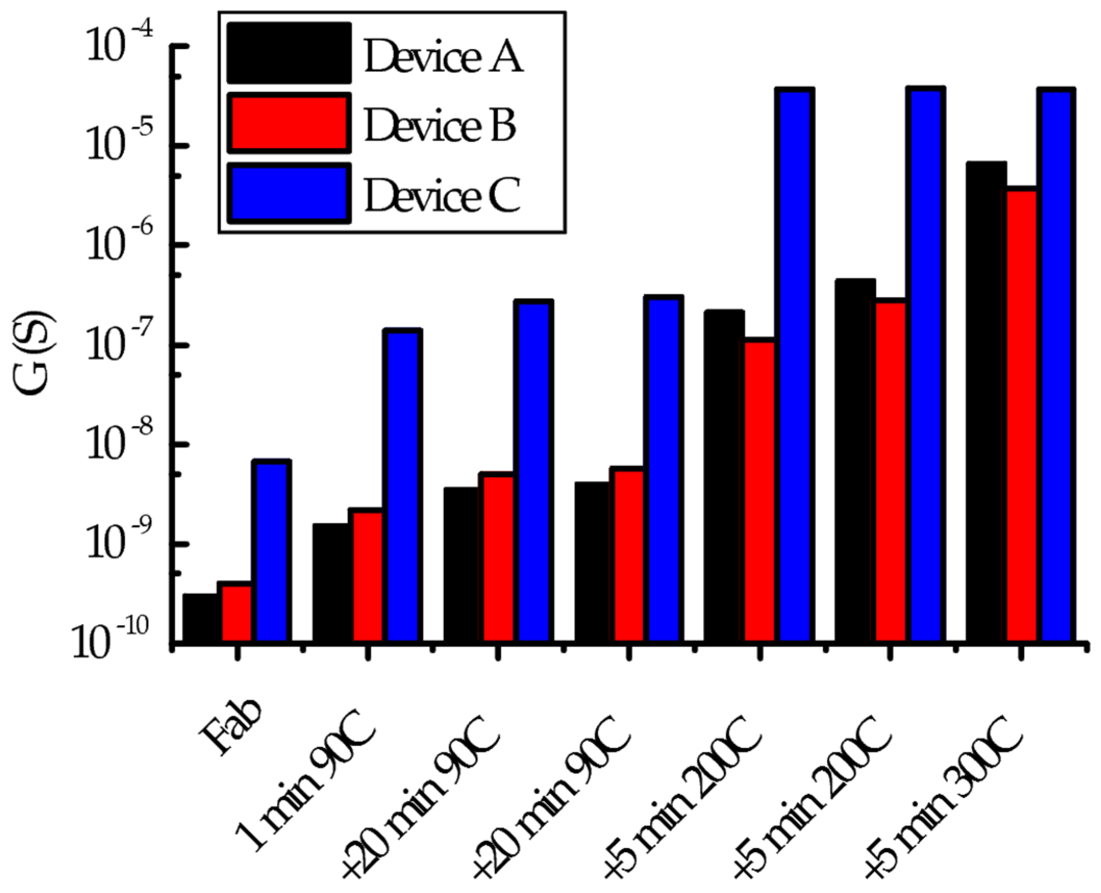
3.2.2. Limitations of the “Double Anneal” Reduction Technique and Search for Alternative Reduction Methods
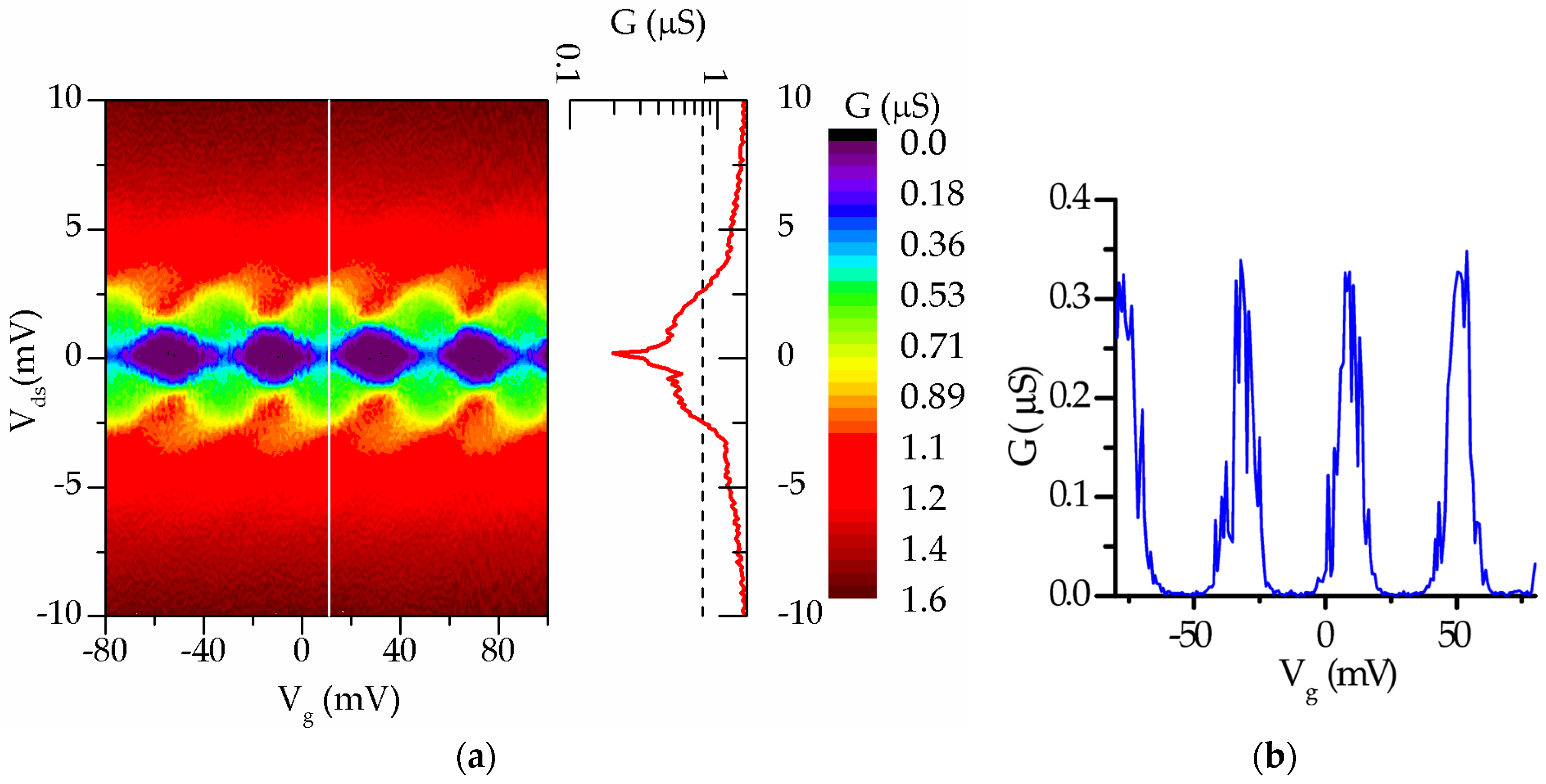
3.2.3. Optimization of Ni-SiO2-Ni Junction Fabrication
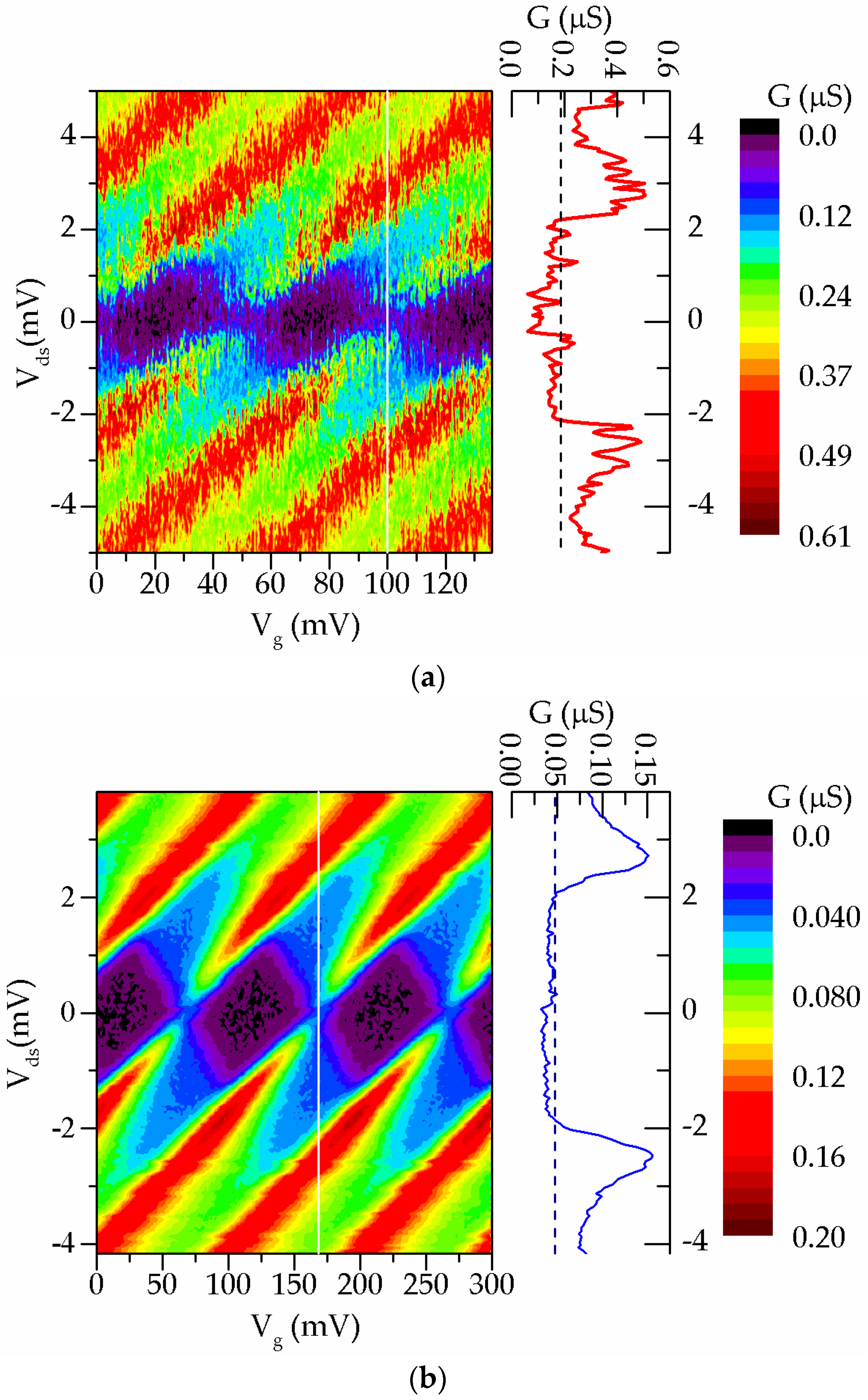
3.2.4. SET Devices with Ni-SiNx-Ni Tunnel Junctions
4. Conclusions
Acknowledgments
Author Contributions
Conflicts of Interest
References
- Fulton, T.A.; Dolan, G.J. Observation of single-electron charging effects in small tunnel junctions. Phys. Rev. Lett. 1987, 59, 109–112. [Google Scholar] [CrossRef] [PubMed]
- Kuzmin, L.S.; Pashkin, Y.A.; Tavkhelidze, A.N.; Ahlers, F.J.; Weimann, T.; Quenter, D.; Niemeyer, J. An all-chromium single electron transistor: A possible new element of single electronics. Appl. Phys. Lett. 1996, 68, 2902–2904. [Google Scholar] [CrossRef]
- Scherer, H.; Weimann, T.; Hinze, P.; Samwer, B.W.; Zorin, A.B.; Niemeyer, J. Characterization of all-chromium tunnel junctions and single-electron tunneling devices fabricated by direct-writing multilayer technique. J. Appl. Phys. 1999, 86, 6956–6964. [Google Scholar] [CrossRef]
- Sillanpää, M.A.; Hakonen, P.J. Titanium single-electron transistor fabricated by electron-beam lithography. Phys. E Low Dimens. Syst. Nanostruct. 2002, 15, 41–47. [Google Scholar] [CrossRef]
- Hobbs, P.C.D.; Laibowitz, R.B.; Libsch, F.R. Ni–NiO–Ni tunnel junctions for terahertz and infrared detection. Appl. Opt. 2005, 44, 6813–6822. [Google Scholar] [CrossRef] [PubMed]
- Zorin, A.B.; Ahlers, F.J.; Niemeyer, J.; Weimann, T. Background charge noise in metallic single-electron tunneling devices. Phys. Rev. B 1996, 53, 13682–13687. [Google Scholar] [CrossRef]
- Pashkin, Y.A.; Nakamura, Y.; Tsai, J.S. Room-temperature Al single-electron transistor made by electron-beam lithography. Appl. Phys. Lett. 2000, 76, 2256–2258. [Google Scholar] [CrossRef]
- Zimmerman, N.M.; Huber, W.H.; Simonds, B.; Hourdakis, E.; Fujiwara, A.; Ono, Y.; Takahashi, Y.; Inokawa, H.; Furlan, M.; Keller, M.W. Why the long-term charge offset drift in Si single-electron tunneling transistors is much smaller (better) than in metal-based ones: Two-level fluctuator stability. J. Appl. Phys. 2008, 104, 033710. [Google Scholar] [CrossRef]
- Rippard, W.H.; Perrella, A.C.; Albert, F.J.; Buhrman, R.A. Ultrathin aluminum oxide tunnel barriers. Phys. Rev. Lett. 2002, 88, 046805. [Google Scholar] [CrossRef] [PubMed]
- Likharev, K.K. Single-electron devices and their applications. Proc. IEEE 1999, 87, 606–632. [Google Scholar] [CrossRef]
- Karbasian, G.; McConnell, M.S.; Orlov, A.O.; Rouvimov, S.; Snider, G.L. Experimental demonstration of single electron transistors featuring SiO2 plasma-enhanced atomic layer deposition in Ni-SiO2-Ni tunnel junctions. J. Vac. Sci. Technol. A 2016, 34, 01A122. [Google Scholar] [CrossRef]
- Karbasian, G.; Fay, P.J.; Xing, H.; Jena, D.; Orlov, A.O.; Snider, G.L. High aspect ratio features in poly(methylglutarimide) using electron beam lithography and solvent developers. J. Vac. Sci. Technol. B 2012, 30, 06FI01. [Google Scholar] [CrossRef]
- Karbasian, G.; Orlov, A.O.; Snider, G.L. Fabrication of nanodamascene metallic single electron transistors with atomic layer deposition of tunnel barrier. J. Vac. Sci. Technol. B 2015, 33, 06FG02. [Google Scholar] [CrossRef]
- McConnell, M.S.; Schneider, L.C.; Karbasian, G.; Rouvimov, S.; Orlov, A.O.; Snider, G.L. Atomic layer deposition of Al2O3 for single electron transistors utilizing Pt oxidation and reduction. J. Vac. Sci. Technol. A 2016, 34, 01A139. [Google Scholar] [CrossRef]
- George, H.C.; Orlov, A.O.; Snider, G.L. Platinum single-electron transistors with tunnel barriers made by atomic layer deposition. J. Vac. Sci. Technol. B 2010, 28, C6L6–C6L8. [Google Scholar] [CrossRef]
- Kulik, I.O.; Shekhter, R.I. Kinetic phenomena and charge discreteness effects in granulated media. Zhur. Eksp. Teor. Fiz. 1975, 68, 623–640. [Google Scholar]
- Beenakker, C.W.J. Theory of Coulomb-blockade oscillations in the conductance of a quantum dot. Phys. Rev. B 1991, 44, 1646–1656. [Google Scholar] [CrossRef]
- Zhou, Y.; Yin, J.; Xu, H.; Xia, Y.; Liu, Z.; Li, A.; Gong, Y.; Pu, L.; Yan, F.; Shi, Y. A TiAl2O5 nanocrystal charge trap memory device. Appl. Phys. Let. 2010, 97, 143504. [Google Scholar] [CrossRef]
- Song, X. Fundamental Studies of Titania-Based High Dielectric Constant Materials. Ph.D. Thesis, University of Illinois at Chicago, Ann Arbor, MI, USA, 2007. [Google Scholar]
- Pierre, M.; Hofheinz, M.; Jehl, X.; Sanquer, M.; Molas, G.; Vinet, M.; Deleonibus, S. Background charges and quantum effects in quantum dots transport spectroscopy. Eur. Phys. J. B 2009, 70, 475–481. [Google Scholar] [CrossRef]
- Groner, M.D.; Elam, J.W.; Fabreguette, F.H.; George, S.M. Electrical characterization of thin Al2O3 films grown by atomic layer deposition on silicon and various metal substrates. Thin Solid Films 2002, 413, 186–197. [Google Scholar] [CrossRef]
- Schneider, L.C. Fabrication of Single Electron Transistors Using Atomic Layer Deposition. Master’s Thesis, University of Notre Dame, Notre Dame, IN, USA, 2014. [Google Scholar]
- Wilk, G.D.; Muller, D.A. Correlation of annealing effects on local electronic structure and macroscopic electrical properties for HfO2 deposited by atomic layer deposition. Appl. Phys. Let. 2003, 83, 3984–3986. [Google Scholar] [CrossRef]
- Fernandez, M.P.H.; Chamberland, B.L. A new high-pressure form of PtO2. J. Less Common Met. 1984, 99, 99–105. [Google Scholar] [CrossRef]
- Friebel, D.; Miller, D.J.; O’Grady, C.P.; Anniyev, T.; Bargar, J.; Bergmann, U.; Ogasawara, H.; Wikfeldt, K.T.; Pettersson, L.G.M.; Nilsson, A. In situ X-ray probing reveals fingerprints of surface platinum oxide. Phys. Chem. Chem. Phys. 2011, 13, 262–266. [Google Scholar] [CrossRef] [PubMed]
- Roschier, L.; Hakonen, P.; Bladh, K.; Delsing, P.; Lehnert, K.W.; Spietz, L.; Schoelkopf, R.J. Noise performance of the radio-frequency single-electron transistor. J. Appl. Phys. 2004, 95, 1274–1286. [Google Scholar] [CrossRef]
- Kano, S.; Azuma, Y.; Tanaka, D.; Sakamoto, M.; Teranishi, T.; Smith, L.W.; Smith, C.G.; Majima, Y. Random telegraph signals by alkanethiol-protected Au nanoparticles in chemically assembled single-electron transistors. J. Appl. Phys. 2013, 114, 223717. [Google Scholar] [CrossRef]
- Xiangning, L.; Tomcsanyi, M.; Orlov, A.O.; Kosel, T.H.; Snider, G.L. Strong cotunneling suppression in a single-electron transistor with granulated metal film island. Appl. Phys. Let. 2006, 89, 43511. [Google Scholar]
- Beloborodov, I.S.; Lopatin, A.V.; Vinokur, V.M.; Efetov, K.B. Granular electronic systems. Rev. Mod. Phys. 2007, 79, 469. [Google Scholar] [CrossRef]
- Kolkovsky, V.; Stübner, R.; Langa, S.; Wende, U.; Kaiser, B.; Conrad, H.; Schenk, H. Influence of annealing in H atmosphere on the electrical properties of Al2O3 layers grown on p-type Si by the atomic layer deposition technique. Solid State Electron. 2016, 123, 89–95. [Google Scholar] [CrossRef]
- Simmons, J.G. Generalized formula for electric tunnel effect between similar electrodes separated by a thin insulating film. J. Appl. Phys. 1963, 34, 1793–1803. [Google Scholar] [CrossRef]
- Kessels, E.; Potts, S.H.P.; van de Sanden, R. Plasma Atomic Layer Deposition. In Atomic Layer Deposition of Nanostructured Materials; Nicola Pinna, M.K., Ed.; Wiley: Weinheim, Germany, 2011; pp. 131–157. [Google Scholar]
- Knechten, C.A.M. Plasma Oxidation for Magnetic Tunnel Junctions; Eindhoven University of Technology: Eindhoven, The Netherlands, 2005. [Google Scholar]
- Foroughi Abari, A. Atomic Layer Deposition of Metal Oxide Thin Films on Metallic Substrates. Ph.D. Thesis, University of Alberta, Alberta, AB, Canada, 2012. [Google Scholar]
- Faes, A.; Jeangros, Q.; Wagner, J.B.; Hansen, T.W.; Van Herle, J.; Brisse, A.; Dunin-Borkowski, R.; Hessler-Wyser, A. In situ Reduction and Oxidation of Nickel from Solid Oxide Fuel Cells in a Transmission Electron Microscope. ECS Trans. (Electrochem. Soc.) 2009, 25, 1985–1992. [Google Scholar]
- Lee, J.-S.; Kim, B.-S. Synthesis and Related Kinetics of Nanocrystalline Ni by Hydrogen Reduction of NiO. Mater. Trans. 2001, 42, 1607–1612. [Google Scholar] [CrossRef]
- Utigard, T.A.; Wu, M.; Plascencia, G.; Marin, T. Reduction kinetics of Goro nickel oxide using hydrogen. Chem. Eng. Sci. 2005, 60, 2061–2068. [Google Scholar] [CrossRef]
- Mani, S.; Saif, T.; Han, J.H. Effect of annealing on the conductivity of electroless deposited Ni nanowires and films. IEEE Trans. Nanotechnol. 2006, 5, 138–141. [Google Scholar] [CrossRef]
- Grigoras, K.; Franssila, S.; Airaksinen, V.M. Investigation of sub-nm ALD aluminum oxide films by plasma assisted etch-through. Thin Solid Films 2008, 516, 5551–5556. [Google Scholar] [CrossRef]
- Pauleau, Y. Interconnect Materials. In Microelectronic Materials and Processes; Levy, R.A., Ed.; Springer: Dordrecht, The Netherlands, 1989; pp. 635–678. [Google Scholar]
- Nagao, K.; Neaton, J.B.; Ashcroft, N.W. First-principles study of adhesion at Cu/SiO2 interfaces. Phys. Rev. B 2003, 68, 125403. [Google Scholar] [CrossRef]
- Srolovitz, D.J.; Safran, S.A. Capillary instabilities in thin films. II. Kinetics. J. Appl. Phys. 1986, 60, 255–260. [Google Scholar] [CrossRef]
- Tu, X.; Gallon, H.J.; Whitehead, J.C. Plasma-assisted reduction of a NiO/Al2O3 catalyst in atmospheric pressure H2/Ar dielectric barrier discharge. Catal. Today 2013, 211, 120–125. [Google Scholar] [CrossRef]
- Zhang, X.; Sun, W.-J.; Chu, W. Effect of glow discharge plasma treatment on the performance of Ni/SiO2 catalyst in CO2 methanation. J. Fuel Chem. Technol. 2013, 41, 96–101. [Google Scholar] [CrossRef]
- Nazarov, A.; Lysenko, V.; Nazarova, T. Hydrogen plasma treatment of silicon thin-film structures and nanostructured layers. Semicond. Phys. Quantum Electron. Optoelectron. 2008, 11, 101–123. [Google Scholar]
- Peña, O.; Muhl, S.; López, W.; Rodríguez-Fernández, L.; Ruvalcaba-Sil, J.L. Hydrogen plasma etching of silicon dioxide in a hollow cathode system. Thin Solid Films 2010, 518, 3156–3159. [Google Scholar] [CrossRef]
- Machlup, S. Noise in semiconductors: Spectrum of two-parameter random signal. J. Appl. Phys. 1954, 25, 341–343. [Google Scholar] [CrossRef]
- Karbasian, G. Fabrication of metallic single electron transistors featuring plasma enhanced atomic layer deposition of tunnel barriers. Ph.D. Thesis, University of Notre Dame, Ann Arbor, MI, USA, 2015. [Google Scholar]
- Karbasian, G.; Orlov, A.O.; Mukasyan, A.S.; Snider, G.L. Single-Electron Transistors Featuring Silicon Nitride Tunnel Barriers Prepared by Atomic Layer Deposition. In Proceedings of the 2nd Joint International EUROSOI Workshop and International Conference on Ultimate Integration on Silicon, EUROSOI-ULIS 2016, Vienna, Austria, 25–27 January 2016; Institute of Electrical and Electronics Engineers Inc.: Vienna, Austria, 2016; pp. 32–35. [Google Scholar]
- Vianello, E.; Driussi, F.; Blaise, P.; Palestri, P.; Esseni, D.; Perniola, L.; Molas, G.; De Salvo, B.; Selmi, L. Explanation of the Charge Trapping Properties of Silicon Nitride Storage Layers for NVMs-Part II: Atomistic and Electrical Modeling. IEEE Trans. Electron. Dev. 2011, 58, 2490–2499. [Google Scholar] [CrossRef]
- Sonoda, K.; Tsukuda, E.; Tanizawa, M.; Yamaguchi, Y. Electron trap level of hydrogen incorporated nitrogen vacancies in silicon nitride. J. Appl. Phys. 2015, 117, 104501. [Google Scholar] [CrossRef]
- Cowell, E.W.; Alimardani, N.; Knutson, C.C.; Conley, J.F.; Keszler, D.A.; Gibbons, B.J.; Wager, J.F. Advancing MIM electronics: Amorphous metal electrodes. Adv. Mater. 2011, 23, 74–78. [Google Scholar] [CrossRef] [PubMed]


| Fabrication Process | Source/Drain Metal | Island Metal | Dielectric | Cycles (nm) | Treatment | Observations |
|---|---|---|---|---|---|---|
| Cross-tie | Pt | Pt | ALD Al2O3 (H2O-based) | 9 (~1 nm) | none | Non-MIM behavior, long-term instability |
| Cross-tie | Pt | Pt | ALD Al2O3 (H2O-based) | 9 (~1 nm) | Post-fab: 5 min, Ar 375 °C | All shorts |
| Cross-tie | Pt | Pt | ALD Al2O3 (O3-based) | 9 (~1 nm) | none | Highly resistive |
| Cross-tie | Pt | Pt | ALD Al2O3 (O3-based) | 9 (~1 nm) | Post-fab: 5 min, Ar 375 °C | Stable but noisy |
| Cross-tie | Pt | Pt | PEALD SiO2 | 15 (~1.5 nm) | none | All shorts |
| Cross-tie | Ni | Ni | PEALD SiO2 | 2 (~0.2 nm) | none | Low conductance, non-MIM behavior |
| Cross-tie | Ni | Ni | PEALD SiO2 | 2 (~0.2 nm) | Post-ALD: 2 min, 5% H2 in Ar 400 °C | Evidence of “pinholes” |
| Cross-tie/Half-Damascene | Ni | Ni | PEALD SiO2 | 12 (~1.1 nm) | Post-ALD: (FGA) 30 min, 5% H2 in Ar 400 °C | Effectiveness limited by agglomeration and noisy |
| Post-Fab: (FGA) 10 min, 5% H2 in Ar 300 °C | ||||||
| Cross-tie/Half-Damascene | Ni | Ni | PEALD SiO2 | 12 (~1.1 nm) | Post-ALD: (RHP) 5 min, H2 plasma 100W 300 °C | Non-MIM behavior, noisy |
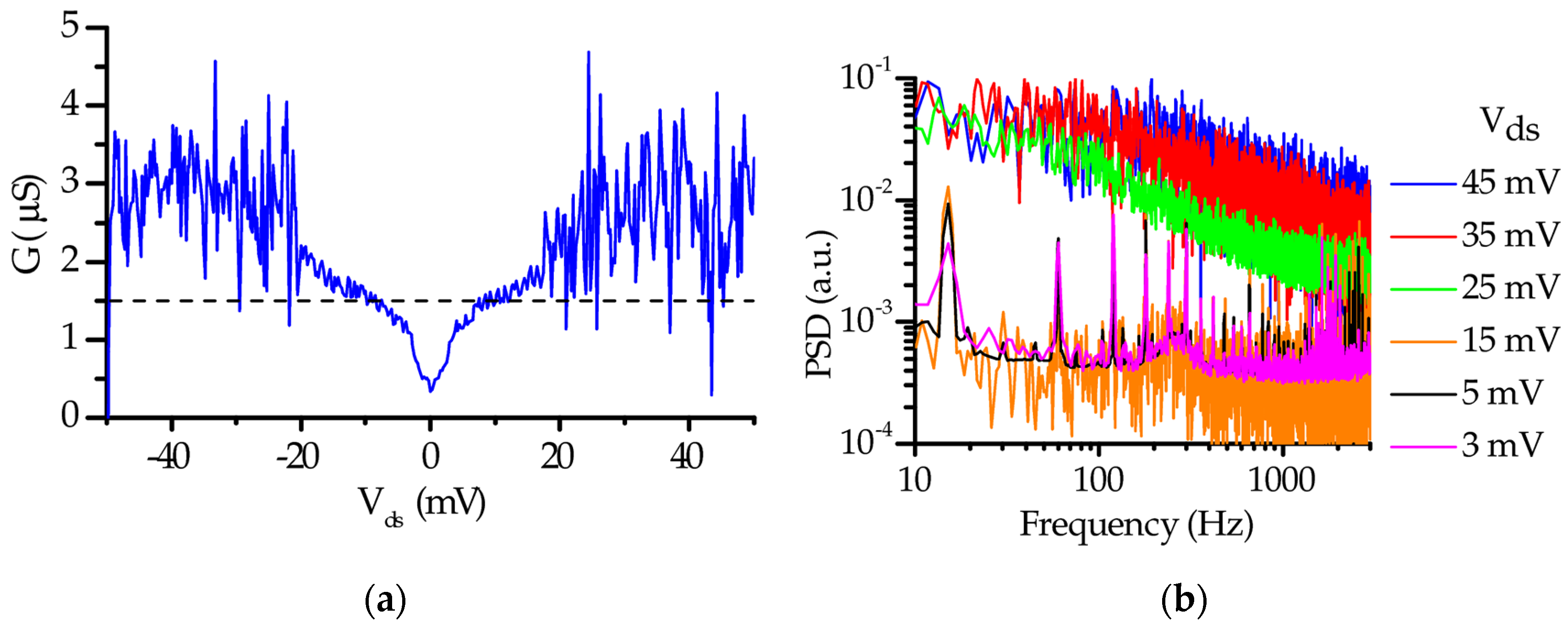
| Cross-tie/Half-Damascene | Ni | Ni | PEALD SiO2 | 12 (~1.1 nm) | Post-ALD: RHP | Highest conductance, non-MIM behavior, noisy when Vds > 15 mV |
| Post-Fab: RHP | ||||||
| Cross-tie/Half-Damascene | Ni | Ni | PEALD SiO2 | 12 (~1.1 nm) | Post-ALD: FGA | Best Performance |
| Post-Fab: RHP | ||||||
| Half-Damascene | Ni | Ni | PEALD SiNx | 21 (~1 nm) | none | Noisy, but no evidence of NiO |
© 2017 by the authors. Licensee MDPI, Basel, Switzerland. This article is an open access article distributed under the terms and conditions of the Creative Commons Attribution (CC BY) license ( http://creativecommons.org/licenses/by/4.0/).
Share and Cite
Karbasian, G.; McConnell, M.S.; George, H.; Schneider, L.C.; Filmer, M.J.; Orlov, A.O.; Nazarov, A.N.; Snider, G.L. Metal-Insulator-Metal Single Electron Transistors with Tunnel Barriers Prepared by Atomic Layer Deposition. Appl. Sci. 2017, 7, 246. https://doi.org/10.3390/app7030246
Karbasian G, McConnell MS, George H, Schneider LC, Filmer MJ, Orlov AO, Nazarov AN, Snider GL. Metal-Insulator-Metal Single Electron Transistors with Tunnel Barriers Prepared by Atomic Layer Deposition. Applied Sciences. 2017; 7(3):246. https://doi.org/10.3390/app7030246
Chicago/Turabian StyleKarbasian, Golnaz, Michael S. McConnell, Hubert George, Louisa C. Schneider, Matthew J. Filmer, Alexei O. Orlov, Alexei N. Nazarov, and Gregory L. Snider. 2017. "Metal-Insulator-Metal Single Electron Transistors with Tunnel Barriers Prepared by Atomic Layer Deposition" Applied Sciences 7, no. 3: 246. https://doi.org/10.3390/app7030246