Article

Overview of 3D Micro- and Nanocoordinate Metrology at PTB

Physikalisch-Technische Bundesanstalt, 38116 Braunschweig, Germany
*
Author to whom correspondence should be addressed.
Appl. Sci. 2016, 6(9), 257; https://doi.org/10.3390/app6090257
Submission received: 15 April 2016 / Revised: 29 August 2016 / Accepted: 30 August 2016 / Published: 12 September 2016
(This article belongs to the Special Issue Design and Applications of Coordinate Measuring Machines)

Abstract

:
Improved metrological capabilities for three-dimensional (3D) measurements of various complex micro- and nanoparts are increasingly in demand. This paper gives an overview of the research activities carried out by the Physikalisch-Technische Bundesanstalt (PTB), the national metrology institute of Germany, to meet this demand. Examples of recent research advances in the development of instrumentation and calibration standards are presented. An ultra-precision nanopositioning and nanomeasuring machine (NMM) has been upgraded with regard to its mirror corner, interferometers and angle sensors, as well as its weight compensation, its electronic controller, its vibration damping stage and its instrument chamber. Its positioning noise has been greatly reduced, e.g., from 1σ = 0.52 nm to 1σ = 0.13 nm for the z-axis. The well-known tactile-optical fibre probe has been further improved with regard to its 3D measurement capability, isotropic probing stiffness and dual-sphere probing styli. A 3D atomic force microscope (AFM) and assembled cantilever probes (ACPs) have been developed which allow full 3D measurements of smaller features with sizes from a few micrometres down to tens of nanometres. In addition, several measurement standards for force, geometry, contour and microgear measurements have been introduced. A type of geometry calibration artefact, referred to as the “3D Aztec artefact”, has been developed which applies wet-etched micro-pyramidal marks for defining reference coordinates in 3D space. Compared to conventional calibration artefacts, it has advantages such as a good surface quality, a well-defined geometry and cost-effective manufacturing. A task-specific micro-contour calibration standard has been further developed for ensuring the traceability of, e.g., high-precision optical measurements at microgeometries. A workpiece-like microgear standard embodying different gear geometries (modules ranging from 0.1 mm to 1 mm) has also been developed at the Physikalisch-Technische Bundesanstalt.

1. Introduction

Following the progressive miniaturization of today’s manufacturing processes, more and more micro- and nanoparts with a complex geometry are applied to numerous industrial products, such as those in the automotive, medical, robotics and telecommunications fields. Full 3D measurements of these micro- and nanoparts with uncertainties down to 100 nm or even below are increasingly in demand [1,2]. For instance, spray holes of fuel injection nozzles are to be fabricated with diameters of less than 100 µm for a better fuel atomization. Measurements of the diameters and of the form and inner surface quality of the spray holes are of crucial importance. The microgears with modules from 1 µm to 1 mm are key components of, e.g., microrobotics and medical devices. Nondestructive measurements and the quality control of both the mould and the replicated gears are of great importance.
Today various techniques are available for full 3D measurements of microparts. One of the most important development trends in industrial dimensional metrology, having the potential to fulfil the requirements to measure complex microparts, is multi-sensor coordinate metrology. This combines the speed of optical measurements with the accuracy and 3D capability of tactile measurements and, more recently, the ability to measure interior features using X-ray computed tomography (CT) [3]. Improved metrological capabilities are needed to ensure the measurement traceability and reliability of the various measurement techniques.
To offer the highly accurate full 3D metrological capability of microparts, a generation of micro-coordinate measuring machines (micro-CMMs) has been developed in the last two decades [4,5,6,7,8,9,10,11,12,13,14]. The first micro-CMM was developed by Peggs et al. [4] at the National Physical Laboratory of the United Kingdom in the year 1999. In its configuration, they applied a mirror corner near the CMM probe as reference mirrors and utilized three laser interferometers and three autocollimators to measure the probe position with respect to the metrology frame. This novel design greatly reduced the Abbe offset, thus offering high 3D measurement accuracy (estimated as 50 nm at the 95% confidence level) over a measurement volume of 50 mm × 50 mm × 50 mm. Almost at the same time, Vermeulen et al. [5] developed a micro-CMM where linear scales are applied to measure the position of the probe tip fully in compliance with the Abbe principle in the x- and y-directions with a motion volume of 100 mm × 100 mm × 50 mm. The design was later commercialized by the Zeiss company in their micro-CMM F25 (unfortunately, F25 is now no longer in the product portfolio of Zeiss). A similar design idea has recently been realized in the micro-CMM “TriNano” with all the three axes measured with the Abbe principle [6]. In the year 2000, Jäger et al. [7] developed a nanopositioning and nanomeasuring machine (NMM) with a motion volume of 25 mm × 25 mm × 5 mm. They applied three miniature laser interferometers and two autocollimators to measure six degrees of freedom (DOFs) of the motion stage with respect to the Zerodur metrology frame, which is fully in compliance with the Abbe principle in all three axes. Using a similar principle, Ruijl [8] built the CMM “Isara” with a measurement volume of 100 mm × 100 mm × 40 mm. Recently, a larger version (“Isara 400”) has been developed by IBS Precision Engineering BV with a motion volume of 400 mm × 400 mm × 100 mm [9].
Various micro-CMM probes have also been developed [4,11,15,16,17,18,19,20,21,22,23,24,25,26,27,28,29,30]. Most of them are mechanical tactile probes working in the contact mode [4,11,15,16,17,18,19]. In their configuration, typically a stylus (having a probing sphere at its free end, and usually fixed to a rigid centre plate/boss at the other end) is suspended by a type of flexure structure, for instance, flexure strips [4,15], slender rods [14,18], flexure hinges [11] or membranes [16]. When the probing sphere is touched and deflected by a workpiece, the flexure structure is deformed due to the probing force. By measuring the deformation via various sensing techniques, for example by means of capacitive sensors [4,15], piezoresistive sensors [16], inductive sensors [11], laser focus sensors [14], a Michelson interferometer combined with an autocollimator [17], or even by means of low-cost DVD pick-up heads [18], the translational motion of the probe sphere in 3D can be derived. Some of the probes [15,16] are realized based on the micro-electro-mechanical systems (MEMS) technique, which offers a much smaller dynamic mass (20 mg) and thus enables a potentially higher measurement speed.
Although being the mostly used probing technique in micro-CMMs and offering outstanding measurement performance (3D uncertainty typically in the order of tens of nanometres), tactile probes have several limiting aspects. The first aspect concerns the probing force and the probing stiffness. A design trade-off needs to be made between the stiffness and the flexibility of the probing element, for instance to avoid damaging the sensitive parts on the one hand, and to overcome the surface forces or inertial loads on the other hand. To overcome this trade-off, the University of Nottingham (UK) has recently developed a probe whose stiffness is variable due to the use of a switchable suspension structure [19]. The second limitation is related to the contact measurement mode. This method has several drawbacks—such as possible surface damage, unwanted adhesion to surfaces, or measurement bias due to the inertia force. In addition, the contact mode microprobes usually apply styli with a limited aspect ratio to achieve a better measurement stability. To mitigate these problems, non-contact mode micro-CMM probes have been developed [21,22,23]. In the non-contact measurement mode, the probes are vibrated and the change of the vibration amplitude due to the probe sample’s interaction is usually applied for measurements. For instance, Bauza et al. [21] developed a high-aspect-ratio microprobe using a probe shank with a diameter of 7 μm having an aspect ratio of 700:1. During the measurements, its probe shank is oscillated in a standing wave. The motion of the free end of the probe shank forms a virtual probe tip to serve as the contact point, thus no spherical ball is required. Claverley et al. [22] developed a novel vibrating tactile probe for which six piezoelectric actuators and sensors are fabricated using electro-discharging machining on the three legs of its triskelion design. However, the shape and stability of the motion trajectory of the non-contact probing tip are a critical issue. Murakami et al. [23] reported that the shaft moved in an elliptical motion in their design. Therefore, a compensation method is applied by measuring the stylus’ displacement using position sensitive detectors (PSDs). However, the PSDs are bulky and consequently limit the available measurement space. The third limitation concerns the measurement loop. The measuring sensors of most of the tactile probes are typically located at the suspending membrane or at the flexure strips and measure the signal, which is being transferred via the probing styli. Consequently, the deformation of the probing styli is “invisible” in the sensor’s readout, which leads to measurement errors. Such a problem becomes much more serious for probes with a smaller styli diameter (d) and a longer styli length (l) as the deformation is inversely proportional to d4 and proportional to l3 [20]. To tackle these problems, a tactile optical probe—well known as the fibre probe today—has been developed at the Physikalisch-Technische Bundesanstalt (PTB) [24]. In contrast to the tactile probes, the measurement signal in fibre probe (i.e., the position of the probing sphere) is directly detected by an optical CCD camera without the mechanical transfer of the probe styli [24]. The advantages are that the probing forces can be very low (1 µN to 100 µN) and stylus tips are available with much smaller diameters (down to 25 µm). The 2D version fibre probe has been used for many years to measure injection nozzles, turbine blade cooling holes, and a variety of other small, tight tolerance features. An upgrade of this probe, the 3D fibre probe, has been commercially available for some time [25]. PTB collaborated with the Werth Messtechnik company are continuing the investigations on this microprobe, which will be detailed in this paper. The design idea of the fibre probe was followed by Cui et al. [26] who proposed a spherical coupling fibre probe as an attempt to overcome the shadowing effect. Some other kinds of tactile-fibre probes have also been proposed, where Bragg grating strain sensors [27], fibre optical displacement sensors [28] and micro-focal-length collimation techniques [29] are applied to measure the position of the probing sphere or of the stylus. In addition, Weckenmann et al. [30] proposed an electrical tunnelling current probe for force-free probing; and Michihata et al. [31] put forward a probe based on the laser trapping technique.
System calibration and performance verification are crucial tasks for 3D micro-coordinate metrology. To qualify, calibrate and verify these micro-CMMs, calibration standards as well as the traceable calibration of these standards are essential. However, this is still a significant challenge today due to the extremely low uncertainty demanded, as is also summarized in a review paper by Claverley et al. [32]. It is extremely difficult to achieve the required calibration uncertainties at calibrated test lengths, due to the limited availability of both high-quality physical standards and metrological services. For example, with the current micro-CMMs exhibiting an uncertainty of 100 nm or less, it is essential for any test length used for verification to be calibrated with an uncertainty that is five- or even ten-times lower, i.e., an uncertainty of better than 20 nm. The micro-CMMs are not covered by the current international standard documents for CMM testing or are only partly covered by them (e.g., VDI 2617 12.1 [33]). Problems also occur when trying to apply the existing acceptance tests defined in ISO 10360-2 [34] to micro-CMMs. According to the test procedures defined in ISO 10360-2, for example, it is required to measure five different calibrated test lengths which are located at seven orientations within the measurement volume of the CMM, four of which must be the space diagonals. However, the shaft length of a micro-CMM probe is usually kept short in order to enhance the measurement stability, which limits its measurement accessibility to all reference features of the calibration artefact. Therefore, the development of a traceable metrological capability and of physical as well as documentary standards is still an urgent task for promoting the commercialization and application of micro-coordinate measuring tools today.
State-of-the-art tactile micro-coordinate metrology has recently been reviewed by Thalmann et al. [35] and three key aspects—stage and metrology system design, probe developments, and system calibration and performance verification—have been well summarized. Therefore, this paper is focused on giving an overview of the research activities carried out at PTB.

2. Instrumentation Developments

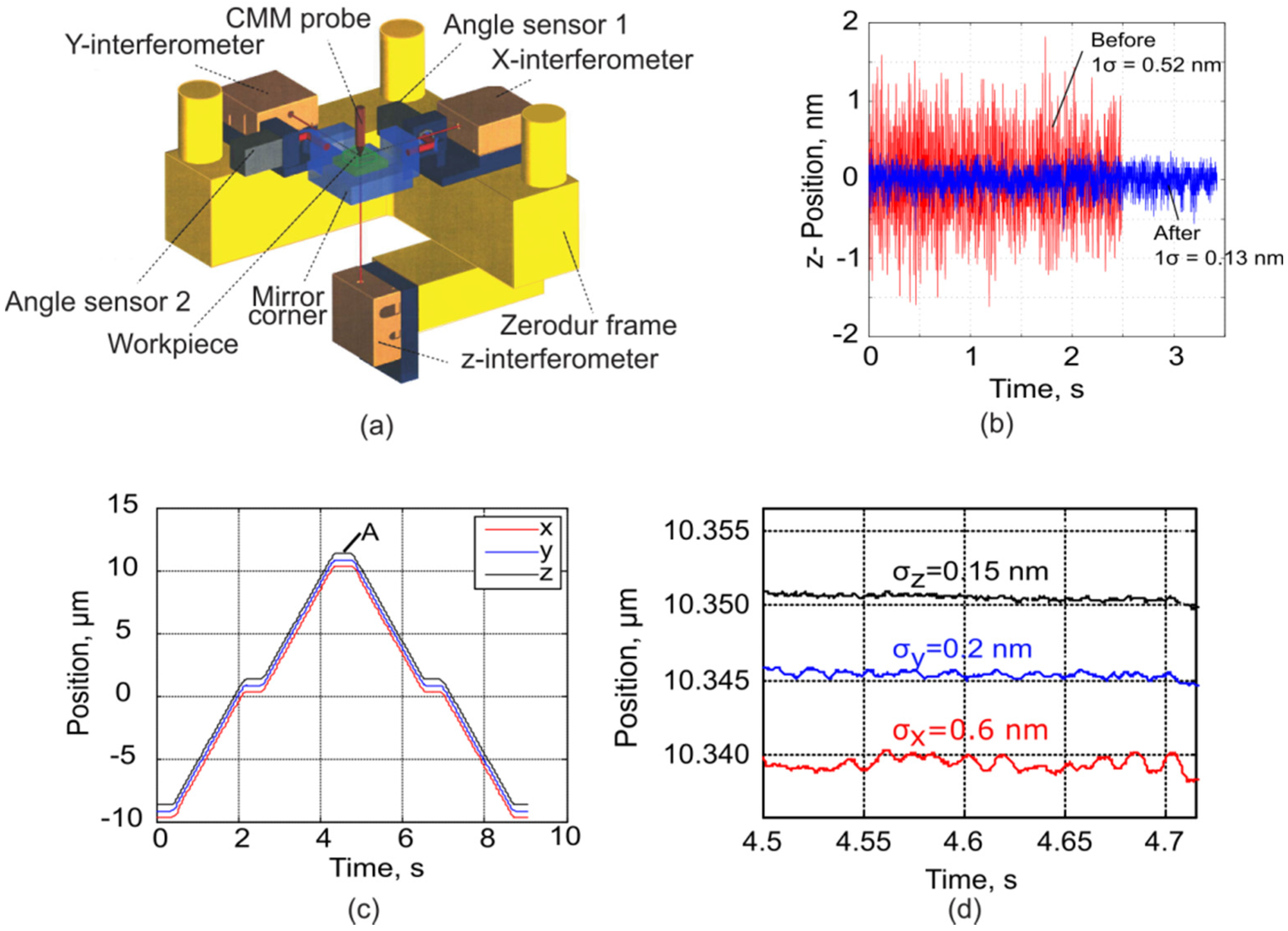
2.1. Upgrade of a Nanomeasuring and Nanopositioning Machine (NMM)

Several micro/nano-CMMs are operated at PTB, including a SIOS NMM, a Zeiss F25, and a Werth VideoCheck UA CMM. Here, we detail the recent upgrade of the NMM in collaboration with the SIOS Company, Ilmenau, Germany.
The measurement principle of the NMM is briefly shown in Figure 1a. Its motion platform consists of a mirror corner which comprises three high-precision planar mirrors attached orthogonally to each other. With three high-precision interferometers (x-, y- and z-interferometer), the displacement of the motion platform can be measured with respect to the metrology frame (Zerodur frame) with a resolution of 0.08 nm. In addition, there are two angle sensors available for measuring all three angular DOFs of the motion platform with a resolution of better than 0.01”. Thus, all six DOFs of the motion platform are accurately measured. The motion platform is moved by three stacked mechanical stages driven by voice coil actuators (not shown). By utilizing a digital signal processor (DSP) servo controller based on the measured six DOF values, the NMM is capable of positioning and measuring with nm accuracy. For micro/nano-CMM measurements, the sample is fixed on the mirror corner and the CMM probe is typically located at the intersection point of three measurement beams of laser interferometers. Thus, the measurement is performed fully in compliance with the Abbe principle along all three axes.
The recent upgrade of the NMM was undertaken with regard to a number of components, as detailed below:
  • The geometry of the corner mirror has been improved to fix samples better so that the stress introduced into the optical component due to the sample fixing is greatly minimized. In addition, the height of the mirrors has been increased so as to allow higher objects (up to 22 mm).
  • The interferometers and the angle sensors have been improved for easier adjustment, better thermal behaviour and better stability.
  • A new motorized spring mechanism has been installed for the weight compensation of the motion stage. As a result, the heat generation of the z-driving motors is greatly reduced, allowing much better temperature stabilization.
  • All the control electronics have been upgraded. They now have an increased servo frequency response up to 1 kHz for better stage control performance.
  • An improved instrument chamber for better thermal and acoustic insulation and an improved vibration damping stage are applied.
To demonstrate how much the performance of the NMM has improved, the positioning noise along the z-axis before and after the upgrade, measured at the same sampling frequency of 6.25 kHz, is compared in Figure 1b. It can be seen that the noise level has been significantly reduced from 1σ = 0.52 nm to 1σ = 0.13 nm. In Figure 1c, a positioning example is shown where the NMM is commanded to move along the x-, y- and z-axes simultaneously by several steps of 10 μm with a speed of 5 μm/s. The position noise along the x-, y- and z-directions after arriving at the target positions is shown in Figure 1d, indicating an excellent positioning and measurement performance.

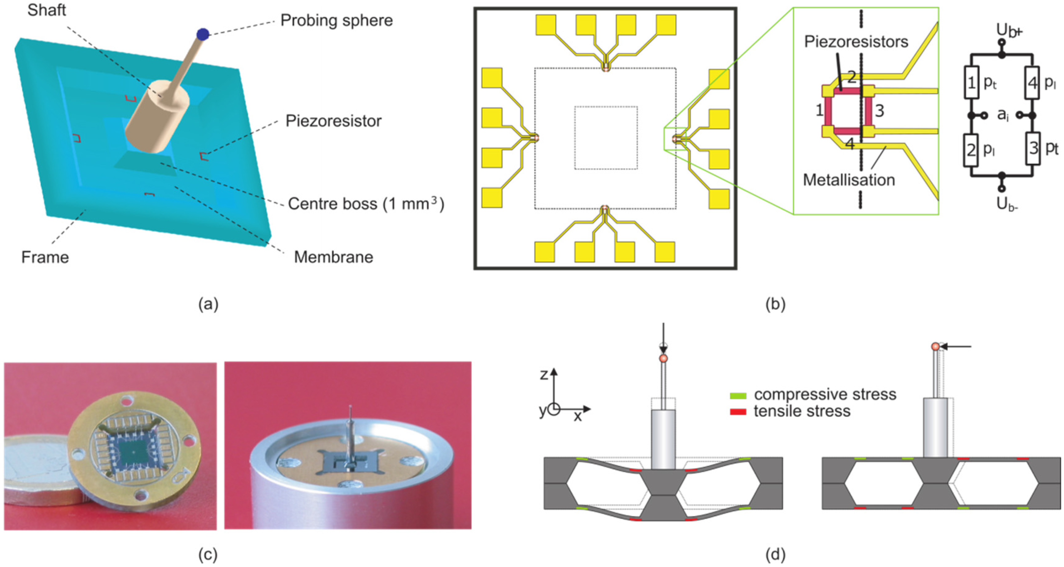
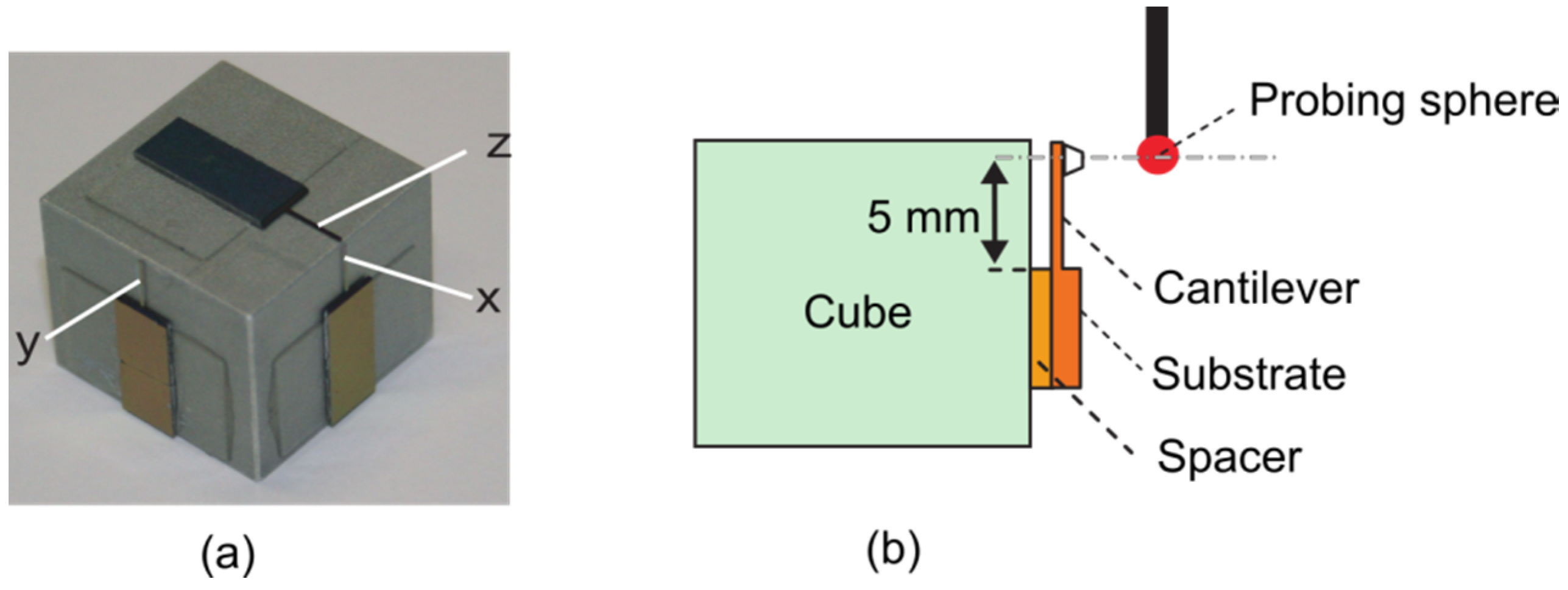
2.2. Boss-Membrane Piezoresistive Microprobe

Several micro-CMM probes are being further developed at PTB, including a boss-membrane piezoresistive microprobe, a fibre probe and probes based on atomic force microscope (AFM).
Figure 2 shows the measurement principle of the boss-membrane piezoresistive microprobe. The fabricated sensor chip includes a centre boss, a membrane having a thickness of tens of micrometres, and a frame. On this chip, a shaft with a length of about 10 mm is glued to the centre boss, and a probing sphere with a diameter of some hundred micrometres is glued to the free end of the shaft. Four groups of piezoresistive sensors, arranged as Wheatstone bridges as shown in Figure 2b, are fabricated on the back of the membrane by the ion implantation technique and act as sensor elements. When the probing sphere touches the measurement object, strains are produced on the membrane by the probing force which leads to changes in the resistances of the piezoresistive sensors. The finite element method (FEM) has been used during the probe design to calculate the position where the maximum strains occur. At these positions, the piezoresistive sensors are located in order to achieve optimum measurement sensitivity. The resistance changes of the sensors are converted into electric signals which are used to determine the probe’s displacement, i.e., for measurement. A photo of such a sensor chip is shown in Figure 2c. The probe was originally designed and fabricated at the Institute for Microtechnology of the Technical University Braunschweig (Braunschweig, Germany) [16], and PTB has applied this technique to micro-CMM applications and has fully investigated its performance in order to achieve improvements [10,36].
A major shortcoming of the probe is its anisotropic stiffness. For instance, for one probe which was investigated in detail, the stiffness values along the x-, y- and z-axes were 208.8 N/m, 313.8 N/m and 5642.9 N/m, respectively. As the styli deformation differs in the different probing directions, such behaviour will lead to form measurement errors, particularly in the scanning measurement mode. In addition, it may also result in a slipping of the probing sphere with respect to the workpiece during the measurements.
To solve this problem, a double triangle design has recently been realized which consists of two structured boss membranes mounted face-to-face as shown in Figure 2d [37]. The states of stress occurring in this structure when it is loaded with vertical and lateral probing forces are also illustrated in the figure. In early stages of the development, the sandwich structure was fabricated by gluing two single chips together whereby one of the chips did not have any electronic components on it. The capillary forces which occurred during the gluing processes yielded a very good alignment of the two chips. Experimental investigations show that the stiffness ratio between the x-, y- and the z-direction has been improved to approximately 2 by the improved design [37]. Currently, a joint research project is also being carried out by the Technical University of Braunschweig in collaboration with PTB to further develop the probe. With the improved design, the probe is capable of measuring with a probing speed of up to 1 mm/s and of achieving a 3D probing repeatability of 50 nm. Testing its probing error according to ISO 10360 has not been done yet.

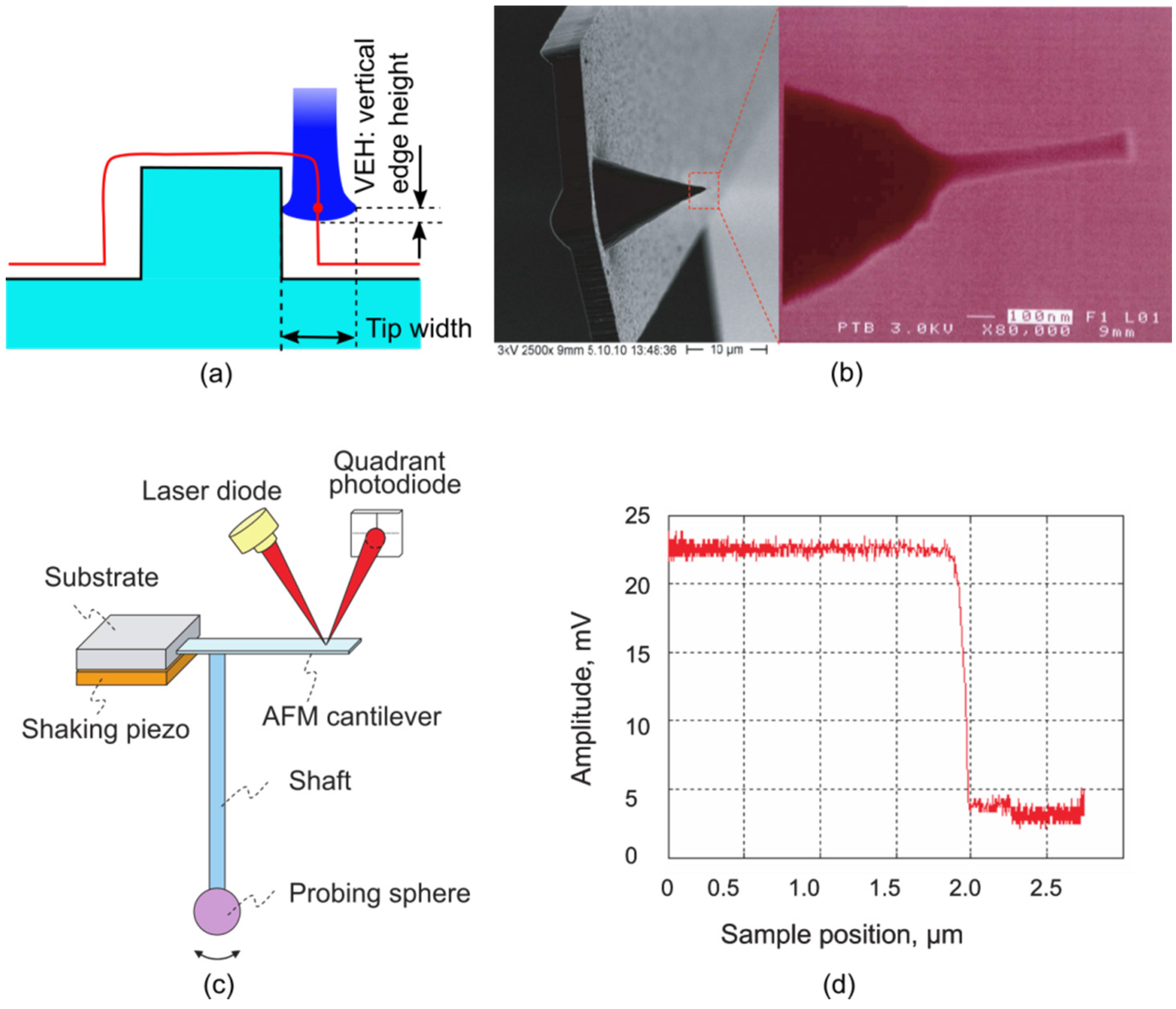
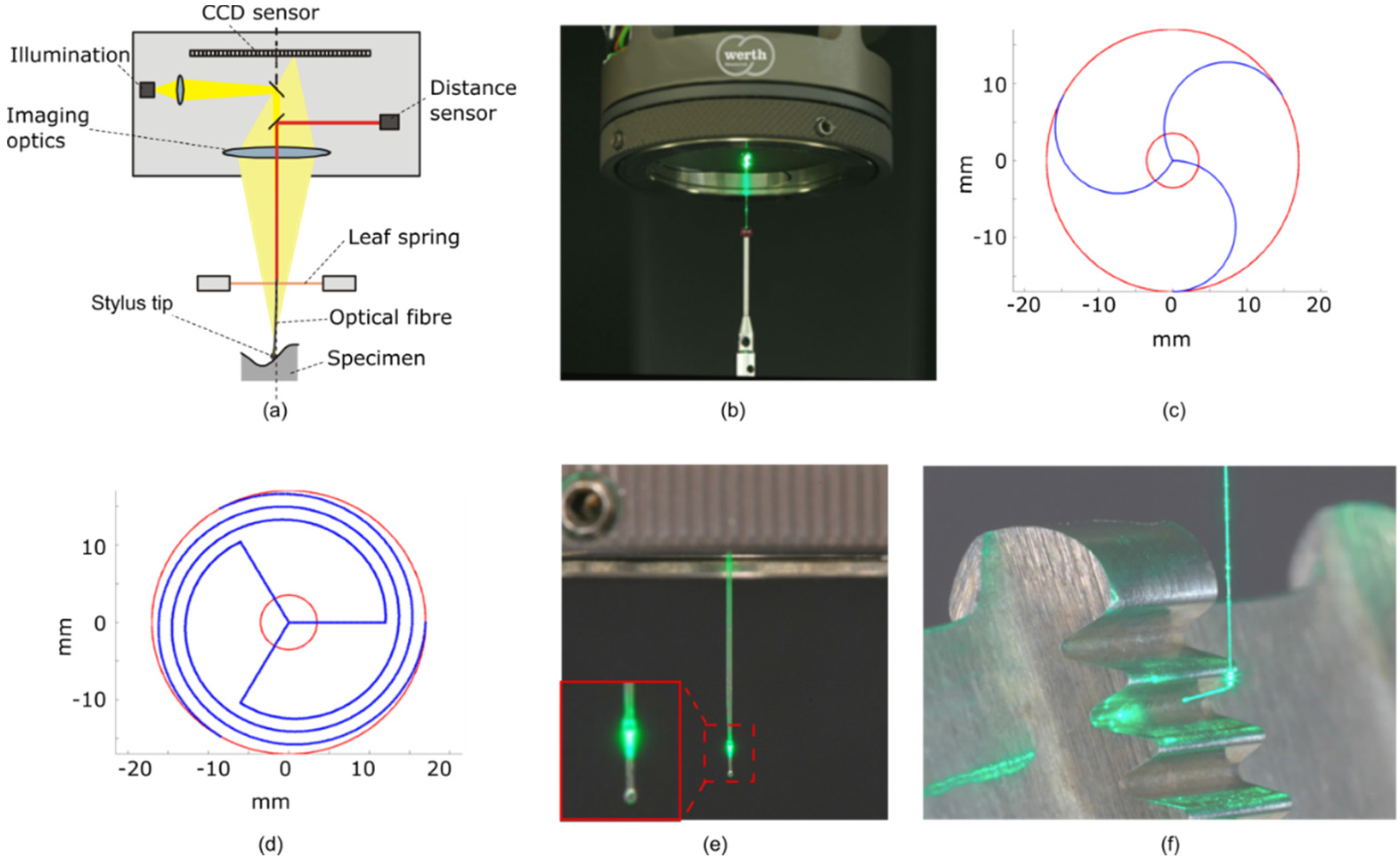
2.3. 3D Tactile-Optical (Fibre) Probe

The principle of a 3D fibre probe is illustrated in Figure 3a. The microprobe consists of an optical glass fibre which acts as the stylus, with a small spherical tip attached to the end. The tip is mounted in the focal plane of the imaging system of an optical coordinate measuring machine (CMM). It is mirror-coated on the lower hemisphere in order to achieve reflectivity. The fibre is fixed to an optical CMM by a three-curved prong leaf spring of low stiffness. This arrangement ensures the flexibility of the probe in all axes.
The determination of the tip position in the axes horizontal to the optics (x- and y-directions) is similar to the well-known 2D fibre probe. The image of the illuminated stylus tip is located in the camera image of the optical CMM by correlation techniques. The stylus position along the z-axis is determined by an optical distance sensor, e.g., based on the Foucault knife-edge principle [38], which measures the height of the upper end of the fibre.
Apart from the 3D measurement function, also the design of the fibre probe has been further improved [25]. For instance, in order to achieve a better isotropic probing stiffness, the design of the leaf spring which suspends the stylus has been optimized by FEM calculations. The original and the optimized designs are shown in Figures 3c,d, respectively. With this improved design, the ratio between the stiffness values in vertical and in horizontal direction could be reduced down to 1.4:1 for standard probes (tip diameter: approximately 250 µm). Furthermore, to eliminate any shadowing effects by the workpiece, a stylus with two spheres has been developed as shown in Figures 3e,f. In such a configuration, the lower sphere is applied to probe the workpiece, whereas the upper sphere is applied for measurements. The displacement ratio between the two spheres was calibrated prior to use. As an advantage, the imaging of the upper sphere is not limited by the workpiece and therefore no shadowing effect occurs. The simplest realization—which consists of a stylus with both spheres arranged vertically with one above the other—is shown in Figure 3e. The distance between the two spheres can be up to a few millimetres. This allows measurements in holes, without the upper sphere being obstructed by the sidewalls of the hole, and thus without reducing the measurement accuracy by this optical effect. However, it is to be mentioned that larger distances between the two spheres lead to larger measurement deviations due to the smaller displacement of the upper sphere. Therefore, the distance between the spheres should be as small as possible, depending on the measurement application.
Another advanced design of the dual-sphere stylus is the L-shaped configuration, as shown in Figure 3f. The stylus consists of a single fibre with two spheres, whereby the fibre is bent below the upper sphere. With such a probe, structures with undercuts can be measured. Here, the bent angle and the length of the bent part can also be adapted to the measurement task.
The 3D fibre probe is capable of achieving a typical probing speed of 0.1 mm/s to 3 mm/s. The specified probing errors are:
-
Single point probing (ISO 10360-5): P = 0.25 µm (probe diameter 250 µm), P = 0.5 µm (probe diameter 40 µm and 100 µm); and
-
Scanning (ISO 10360-4): THN = 1.5 µm (probe diameter 250 µm), THN = 2 µm (probe diameter 40 µm and 100 µm).

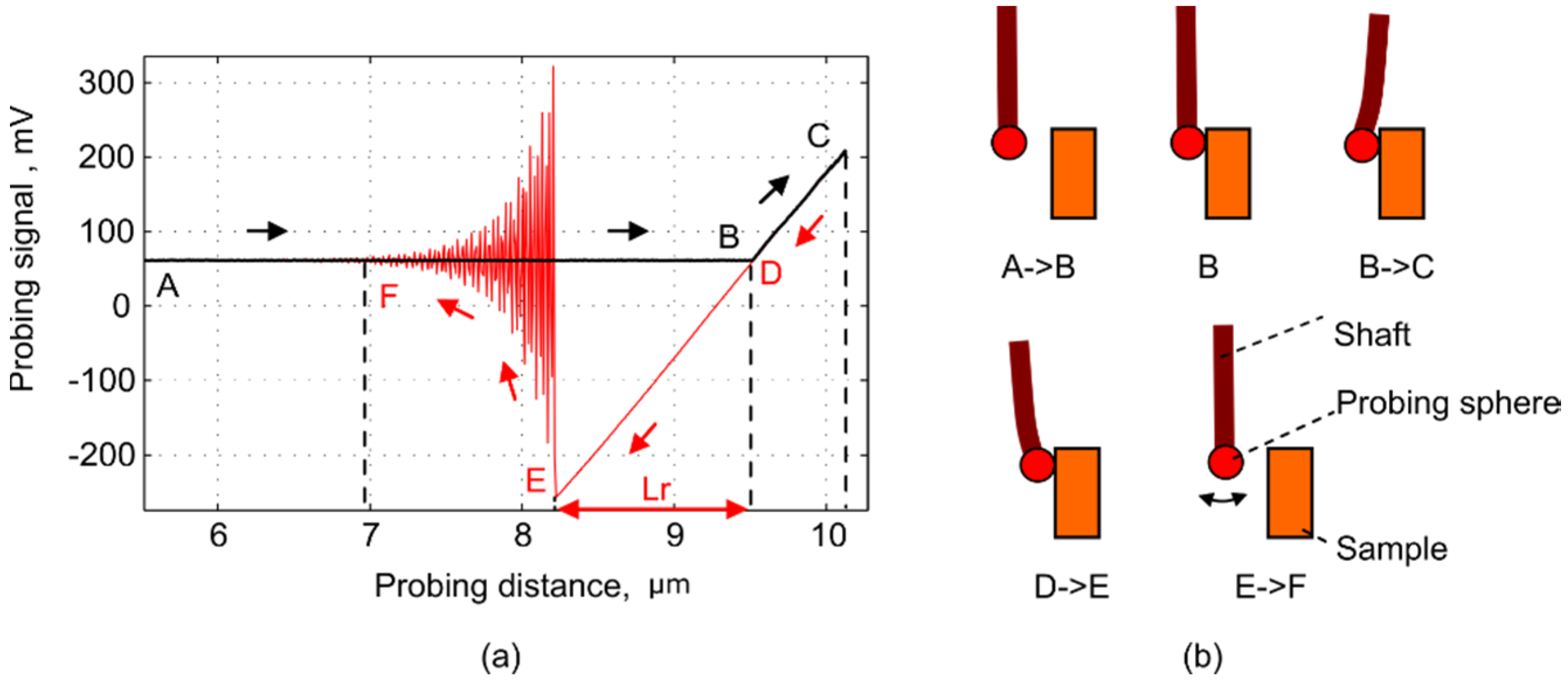
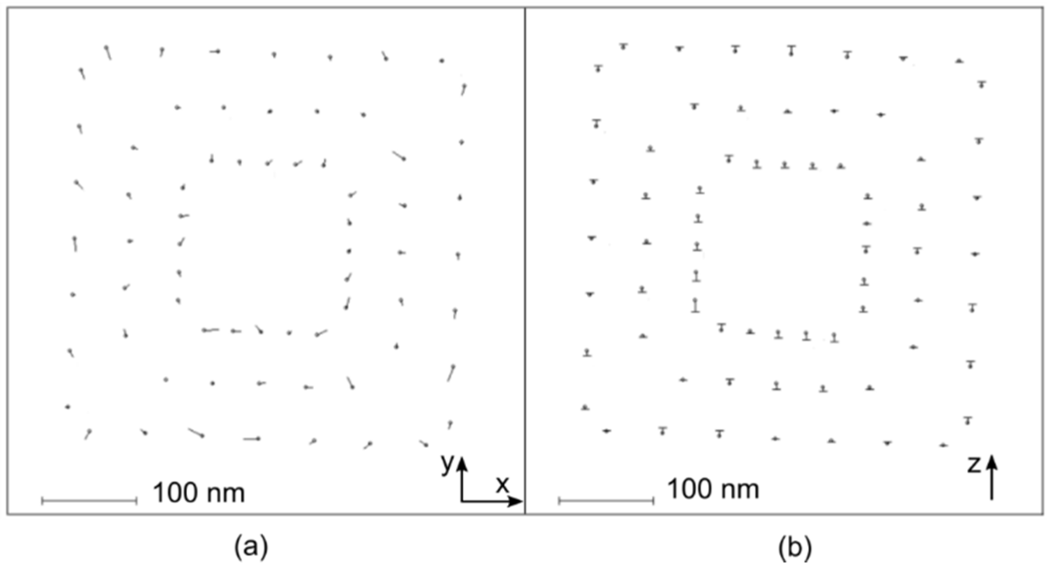
2.4. AFM-Based 3D Probes

Although the diameter of the smallest micro-CMM probe may be as small as 25 µm, it is still too large to measure 3D structures with sizes of a few micrometres or even below. There is a metrology gap between AFMs—the most popular used coordinate measuring techniques for nanostructures—and micro-CMMs. To fill this gap, another idea is a type of 3D probe based on the AFM technique. At PTB, we have developed a 3D-AFM [39] and the so-called assembled cantilever probe [40], which is promising to fill this gap.
The measurement principle of the 3D-AFM developed by PTB is shown in Figure 4a. It utilizes flared AFM tips. Such tips have an extended geometry near their free end which enables the probing of steep and even undercut sidewalls. The probe element can be regarded as a disc; however, due to its tiny size, it still has a high spatial resolution. Similar to conventional AFMs, the 3D-AFM can measure in contact, intermittent and non-contact mode. Furthermore, a vector approach probing (VAP) method has been applied for enhancing the measurement flexibility and for reducing tip wear [24]. Our preliminary uncertainty estimation indicates that the 3D-AFM is capable of measuring the feature width of nanostructures with an expanded uncertainty down to 1.6 nm (at a confidence level of 95%).
Currently, such flared probes are commercially available with a diameter up to 850 nm and an effective stylus length of 7.5 µm [41]. However, the technology can be expanded by building larger flared tips with diameters of a few micrometres and styli lengths of tens of micrometres using, e.g., Focused Ion Beam (FIB) milling or FIB induced deposition techniques.
However, due to the limited speed of the FIB microfabrication technique, the size of its manufacturable probing elements is still limited. To further expand the AFM technique for full 3D measurements, a type of assembled cantilever probe (ACP) has also been proposed [40]. Compared to the flared tip where the probing element is directly fabricated on the tip, the ACP technique applies microassembling techniques to create a probing stylus. The ACP also has the advantages of the AFM technique, such as high measurement sensitivity, very low measurement forces (µN to nN level), a compact structure, low fabrication costs and the ease of probe exchanges. Additionally, the ACP probe is mechanically and electrically compatible with commercial AFMs. It could therefore be applied directly in commercial AFMs to extend their functions from surface topography measurements to 3D measurements, if some minor software modifications are provided.
Due to its low probing stiffness (typically about 1.5 N/m in lateral directions), the 3D-ACP probe is usually used for point-to-point measurements. It is capable of performing measurements with a probing speed of up to 100 μm/s. It has a probing repeatability of approximately 25 nm (p-v) along the z-axis, and of approximately 130 nm (p-v) in full 3D, as shown in Figure 5. Testing of its probing error according to ISO 10360 has not been performed yet.

3. Calibration Artefacts

Calibration artefacts are essential for acceptance tests, as well as for the calibration and verification of micro-CMMs. Several categories of calibration artefacts have been developed at PTB for calibrations of, for instance, the probing force and stiffness, geometric errors, contour and microgear measurements. This section introduces some state-of-the-art calibration artefacts developed at PTB.

3.1. Microforce Calibration Standard

To calibrate the probe’s force and stiffness, a convenient method is to apply a reference spring, whose spring constant has been calibrated by, e.g., means of a compensation balance before usage [42]. An application example was introduced in [36]; however, it is only suitable for calibrating the z probing axis due to its size limit.
To overcome this problem, a new artefact has been fabricated as shown in Figure 6. The artefact consists of three cantilevers marked as “x”, “y” and “z” used as reference springs, whose spring constant has been calibrated in prior. The cantilevers and their substrates are made from silicon using etching techniques. The substrates are glued to an aluminium cube with a glass plate (thickness: 0.2 mm) inserted as a spacer. This glass spacer ensures that the cantilever will not contact the aluminium cube in its free standing and bent states. Near the free end of the cantilever, a trapezoid-shaped tip is fabricated. It is used for loading the probing forces at a known position. As the spring constant of the reference cantilever depends on the position where the force is loaded, the cantilever should be calibrated and used for calibration with forces loaded at the given position. Using such a device, we calibrated the x-, y- and z-stiffness of a boss-membrane 3D probe to be 208.8 N/m, 313.8 N/m and 5642.9 N/m, respectively, as mentioned earlier.
Adhesive forces are observed during the probing process resulting in sticking between the probing sphere and the sample [20]. Such adhesive forces may be attributed to several factors such as atomic/molecular interaction forces, capillary forces, electrostatic forces etc. Since the probing forces of micro/nano-CMMs are only in the order of milli- or micronewtons, the adhesive forces may impact the CMM’s measuring/scanning performance significantly.
Such adhesive forces can also be characterized using the force calibration standard. Figure 7 shows an example where the adhesive force of an ACP probe is characterized. Figure 7a shows a typical probing curve, which depicts the cantilever bending signal vs. the probing distance. For ease of explanation, the curve is marked with letters “A” to “F” to indicate different probe-sample interaction states as shown in Figure 7b. B is the point where the probing sphere begins to contact the sample. This point is calculated as the zero force contact point. In B → C, the probe moves towards the sample. The probing force leads to a positive change of the probing signal, which is quasi-linear with respect to the probing distance. At point C, the motion is stopped and the probing sphere begins to retract from the sample. In C → D, the probing sphere undergoes the reverse trajectory to that of B → C and no hysteresis is found. During D → E, the probing sphere sticks to the sample. The adhesive forces lead to a negative change of the probe signal. At point E, the probing sphere begins to separate from the sample. In E → F, a type of damped oscillation can be seen, which is caused by the release of the adhesive forces on the bent probe. The adhesive forces Fa can be calculated as the probing forces at point E according to Hooke’s law:
F a = k x L r
Here, kx is the spring constant of the probe in the x-direction and Lr is the probing distance needed for separating the probing sphere and the sample.
In this study (sample: sapphire sphere with Ø = 2 mm; probing sphere: sapphire sphere, Ø = 0.12 mm; relative humidity: 46% ± 2%; temperature: 20.5 ± 0.5 °C), we measured Lr = 1.31 μm and estimated adhesive forces of 2.06 μN according to the calibrated reference spring constant kx = 1.575 N/m.

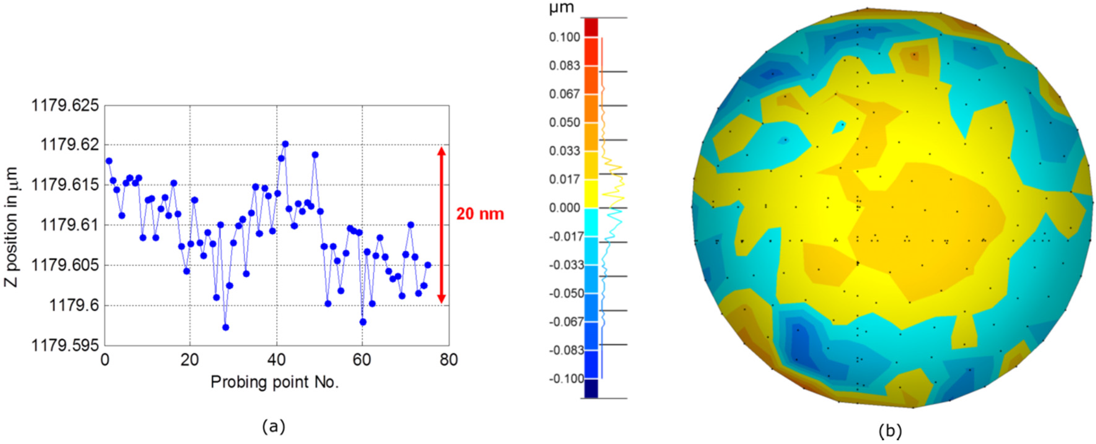
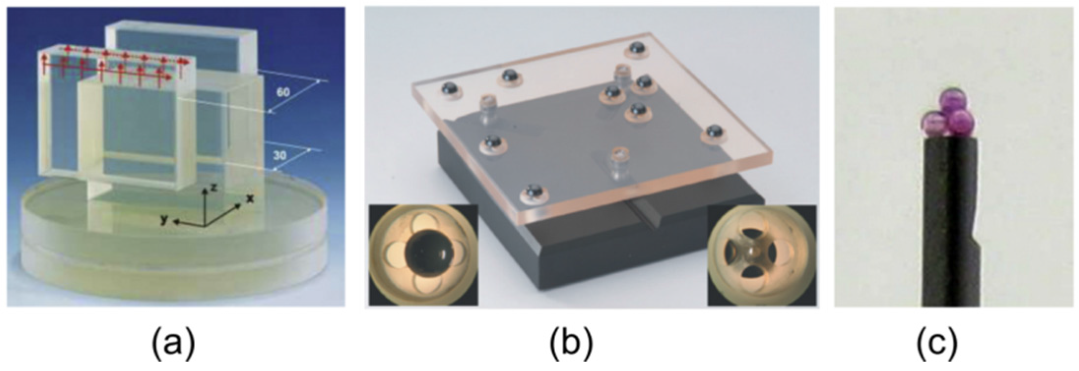
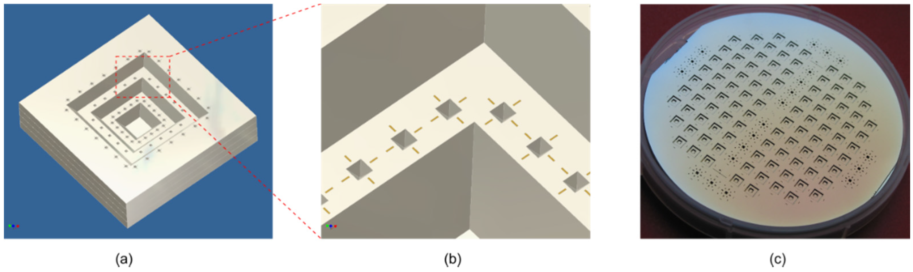
3.2. 3D Aztec Artefact

Geometry calibration standards are essential for the verification or calibration of geometric errors of micro-CMMs. A number of standards have been developed worldwide. Most of them look like a miniature version of popular artefacts applied in large CMMs, for instance, mini ball bar [43], mini ball array [44] or mini ball plate. Photos of some representative calibration artefacts studied at PTB are illustrated in Figure 8.
However, there is a practical limit in applying the artefacts mentioned above. The surface area of reference planes/spheres measurable by microprobes is limited by either the structure of the artefacts or the styli length, consequently impacting the calibration accuracy. In addition, the precise assembling of tiny reference spheres on substrates is also not a trivial task.
To mitigate the problems mentioned above, recently a type of 3D Aztec artefact manufactured from crystal silicon using the wet-etching technique has been developed. One basic unit of the Aztec artefact is shown in Figure 9a. It has a pyramidal shape and consists of a few plateaus. On each plateau, micro-pyramidal marks are fabricated, as detailed in Figure 9b. To calibrate the marks, usually four sidewall planes of marks are measured and their intersection point is calculated as the reference coordinate. In the given design example, the overall size of one pyramid artefact is 6.5 mm × 6.5 mm × 1.4 mm. A photo of a fabricated Aztec artefact in 4-inch wafer size is shown in Figure 9c. It can be conveniently sawed into a suitable size to fit the measurement volume of different micro-CMMs.
The Aztec artefact has several advantages. For instance, the artefact can be mass-produced using the wet-etching technique cost-effectively; due to the crystal nature of the silicon material, the marks have high sidewall surface quality and well-defined geometry (angle between sidewalls and upper surface: 54.7°); the layout of the artefact has a wide open space from the top, offering better accessibility for the probing styli.
Figure 10 shows the repeatability of a calibration of the 3D Aztec artefact using the NMM equipped with a boss-membrane probe. Two repeated measurements are run, with each offering a set of reference coordinates. Their coordinate difference is shown as vectors for the x- and y-coordinates in Figure 10a and that for the z-coordinate in Figure 10b. The scale of the vectors is shown in the bottom left region of the plot. It can be seen that for most measurements, the deviation is less than 10 nm, indicating excellent measurement repeatability.

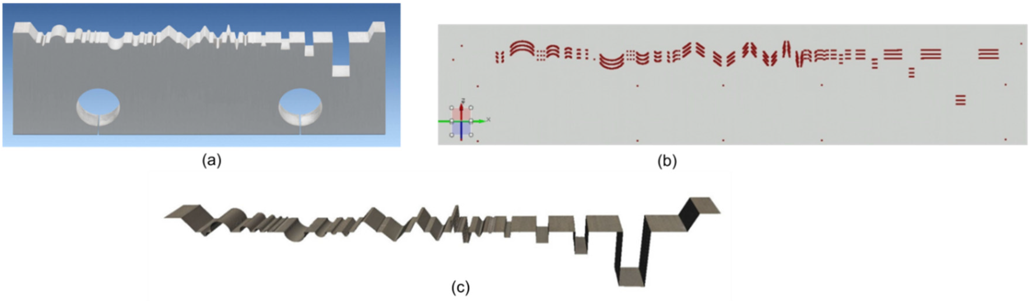
3.3. Micro-Contour Standard

To ensure traceability, especially for high-precision optical measurements at microgeometries, a task-specific micro-contour standard was developed in cooperation between the Alicona Company, IPK-Fraunhofer and PTB. This standard is a further development of a standard presented in [45] and, in contrast to the former standard, is calibrated by tactile probing. The micro-contour standard is made of tungsten carbide, is manufactured by wire-EDM at IPK-Fraunhofer and has a diffusely reflecting surface of Rz ≈ 1.5 µm. It is, therefore, well suited for optical measuring tools such as confocal and focus variation instruments. The external size of the standard is 47 mm × 15 mm × 3 mm with different spherical and prismatic geometric elements on top, as shown in Figure 11a. These elements have dimensions of 0.05 mm up to 5 mm and represent different measurands like radii, angles and step heights. The form deviations of the geometrical elements are in the range of a few tenths of a micrometre.
The micro-contour standards are calibrated by tactile single-point probing, usually as working standards at IPK-Fraunhofer, currently using a Zeiss CMM O-Inspect with a probing sphere of Ø 300 µm. The uncertainties amount to about 1.2 µm for radii, 0.2° for angles and 0.6 µm for step heights. For some special purposes which require lower uncertainty, the standards are calibrated as reference standards at PTB. For this, a Zeiss micro-CMM F25 is used with a probing sphere of Ø 120 µm and very low contact forces of approximately 1 mN. The probing deviation of the F25 according to ISO 10360 determined at different reference spheres of Ø 1 mm up to Ø 10 mm amounts to PF < 0.15 µm (form error) and PS < 0.07 µm (size error). The standards are measured in a horizontal position and the geometric elements are probed in three different traces: 1 mm, 1.5 mm and 2 mm below the front face. Each geometric element in each trace is measured with 50 points, which result in about 10,800 points overall, as shown in Figure 11b. The calibration results are determined from the 3D geometrical elements with 3 × 50 points each. Figure 10c shows an overview scan result of the standard obtained with an optical focus variation instrument (Alicona InfiniteFocus) with 5× magnification. For the testing of optical instruments, the magnification used is adapted to the size of the geometrical element to be measured.
To test the suitability of using the standard, comparison measurements were carried out between the InfiniteFocus and the F25 at four different standards. The results agree with respect to the measurement uncertainty stated as summarized in Table 1.

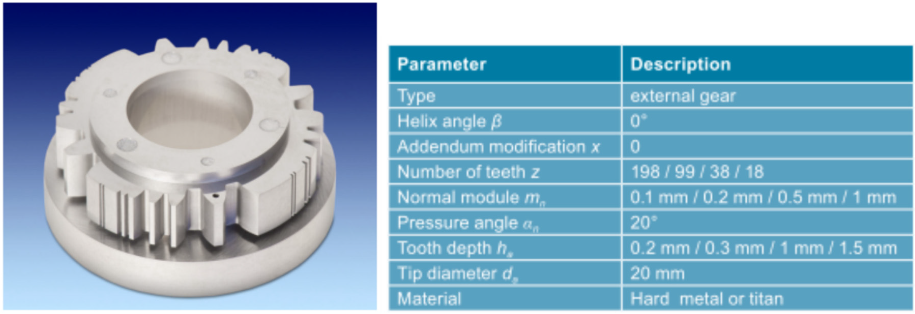
3.4. Microgear Standard

Microgears with transverse modules between 1 µm and 1 mm have become an indispensable part of modern production [46]. They are used in medical devices, semi-conductor manufacturing, microrobotics and precision engineering and are, thus, increasingly gaining in economic relevance. For these gears, a minimum amount of material and simultaneous a maximum amount of precision and efficiency are required. For the implementation of these requirements, reliable quality assurance and, thus, reliable measurement technology are indispensable. However, suitable micro-measurement standards and comparison concepts, with the aid of which the measurements are reliably traceable to the “metre”, the SI unit of length, have been lacking so far.
PTB has recently developed a workpiece-like microgear measurement standard as shown in Figure 12 with detailed design parameters. The standard artefact embodies different gear geometries on one component. It has modules ranging from 0.1 mm to 1 mm, being adapted to the requirements of industry. The design allows measurements with tactile and optical sensors as well as CT procedures.
To demonstrate the quality of the fabricated microgear standard, the measured profiles of a spur gear tooth of the standard are shown in Figure 13. It can be seen that the form deviations are smaller than 0.5 µm at both the profile and the helix scans. The microgear measurement standard has been calibrated using the micro-CMM F25 at PTB and was used in a national intercomparison with a broad range of measuring machines involved. For more information, the reader is referred to [47,48].

4. Conclusions

Micro-coordinate measuring machines (micro-CMMs) are being increasingly applied for accurate 3D measurements of micro/nano parts such as injection nozzles, turbine blades, microholes, and a variety of other small, tight tolerance features. Today, the developments of calibration standards as well as the metrology capabilities are crucially required for acceptance tests, along with the calibration and verification of these micro-CMMs. To satisfy these demands, a number of research activities are being carried out at PTB. An overview of some recent developments concerning instrumentation and calibration standards is given in this paper.
An ultra-precision nanopositioning and nanomeasuring machine (NMM) has been upgraded focusing on its mirror corner, interferometers and angle sensors, as well as its weight compensation, its electronic controller, its vibration damping stage and its instrument chamber. The upgrade has significantly reduced its positioning noise, e.g., from 1σ = 0.52 nm to 1σ = 0.13 nm for the z-axis.
Further developments of several microprobes have been detailed, including the boss-membrane piezoresistive probe, the tactile-optical fibre probe and the AFM based probes. The 3D fibre probe has been significantly improved concerning its 3D measurement capability, isotropic probing stiffness and the design of dual-sphere probing styli. The development of a 3D-AFM and of assembled cantilever probes (ACPs) offers full 3D measurements of parts with sizes from a few micrometres to tens of nanometres. This is promising for filling the metrology gap between AFMs and micro-CMMs.
Further developments of calibration standards for force, geometry, contour and microgears have been introduced. A reference spring artefact applicable for calibrating the 3D probing stiffness as well as for characterizing the probing adhesive force has been presented. An Aztec artefact, which applies micromachined micro-pyramidal marks for defining reference coordinates in 3D space, has also been presented. Compared to conventional calibration artefacts, it has advantages such as high surface quality, well-defined geometry and cost-effective manufacturing. A task-specific micro-contour calibration standard for ensuring the traceability, especially of high-precision optical measurements at microgeometries, has been introduced. A workpiece-like microgear standard embodying different gear geometries (modules ranging from 0.1 mm to 1 mm) has been presented.
Unfortunately, despite the large development and research efforts, the take-up of the micro-coordinate measurement technique is currently quite low. The reasons for this are multifold, for instance, the high purchasing and running costs, low measurement throughput, and the lack of generally accepted physical and documentary standards. Therefore, more research and development work is expected in the future with a possible emphasis on more cost-effective instrumentation, better dynamics properties and measurement strategies for higher measurement throughput, multi-sensor and data fusion techniques to merge the advantages of different sensing techniques, as well as the further development of physical and documentary standards.

Acknowledgments

The authors would like to thank Matthias Hemmleb of the m2c company and Denis Dontsov of the SIOS company for their kind help and excellent support.

Author Contributions

G.D. contributed the research results of § 2.1, § 2.4 and § 3.1; S.B. and G.D. contributed that of § 2.2 and § 3.2; U.N.-R., M.N. and M.S. contributed that of § 2.3, § 3.3 and § 3.4, respectively; G.D. wrote the paper with the supports from all co-authors.

Conflicts of Interest

The authors declare no conflict of interest.

References

  1. Hansen, H.N.; Carneiro, K.; Haitjema, H.; De Chiffre, L. Dimensional micro and nanometrology. CIRP Ann. Manuf. Technol. 2006, 55, 721–743. [Google Scholar] [CrossRef]
  2. Mattsson, L. Metrology of micro-components—A real challenge for the future. In Proceedings of the 5th International Seminar on Intelligent Computation in Manufacturing Engineering (CIRP ISME ’06), Ischia, Italy, 25–28 July 2006; pp. 547–552.
  3. Multi-Sensor Metrology for Microparts in Innovative Industrial Products. EMRP Project. Available online: https://www.ptb.de/emrp/microparts-project.html (accessed on 8 April 2016).
  4. Peggs, G.N.; Lewis, A.J.; Oldfield, S. Design for a compact high-accuracy CMM. CIRP Ann. Manuf. Technol. 1999, 48, 417–420. [Google Scholar] [CrossRef]
  5. Vermeulen, M.M.P.A.; Rosielle, P.C.J.N.; Schellekens, P.H.J. Design of a high-precision 3D-coordinate measuring machine. CIRP Ann. Manuf. Technol. 1998, 47, 447–450. [Google Scholar] [CrossRef]
  6. Van Riel, M.; Moers, T. Nanometer uncertainty for a micro price. Mikroniek 2010, 50, 13–17. [Google Scholar]
  7. Jäger, G.; Manske, E.; Hausotte, T.; Büchner, H.J. Laserinterferometrische Nanomessmachinen. In Sensoren und Messsysteme 2000. VDI Berichte 1530; VDI Verlag: Düsseldorf, Germany, 2000; pp. 271–278. [Google Scholar]
  8. Ruijl, T.A.M. Ultra Precision Coordinate Measuring Machine—Design, Calibration and Error Compensation. Ph.D. Thesis, Technische Universität Darmstadt, Darmstadt, Germany, 1 May 2001. [Google Scholar]
  9. ISARA 400 ULTRAPRÄZISIONS-KOORDINATENMESSMASCHINE, Precision Engineering BV. Available online: http://www.ibspe.de/category/isara-400-ultraprazisions-koordinatenmessmaschine.htm (accessed on 8 April 2016).
  10. Cao, S.; Brand, U.; Kleine-Besten, T.; Hoffmann, W.; Schwenke, H.; Bütefisch, S.; Büttgenbach, S. Recent developments in dimensional metrology for microsystem components. Microsyst. Technol. 2002, 8, 3–6. [Google Scholar] [CrossRef]
  11. Küng, A.; Meli, F.; Thalmann, R. Ultraprecision micro-CMM using a low force 3D touch probe. Meas. Sci. Technol. 2007, 18, 319–327. [Google Scholar] [CrossRef]
  12. Werth VideoCheck® UA, Werth Messtechnik GmbH. Available online: http://www.werth.de/de/unser-angebot/produkte-nach-kategorie/koordinatenmessgeraete/fuer-labor-und-messraum/werth-videocheck-ua.html (accessed on 8 April 2016).
  13. UMAP Vision System Type2 Ultra UMAP404. Mitutoyo Corporation. Available online: http://ecatalog.mitutoyo.com/UMAP-Vision-System-TYPE2-Series-364-Micro-Form-Measuring-System-C1577.aspx (accessed on 8 April 2016).
  14. Fan, K.C.; Fei, Y.T.; Yu, X.F.; Chen, Y.J.; Wang, W.L.; Chen, F.; Liu, Y.S. Development of a low cost micro-CMM for 3D micro/nano measurements. Meas. Sci. Technol. 2006, 17, 524–532. [Google Scholar] [CrossRef]
  15. Pril, W.O. Development of High Precision Mechanical Probes for Coordinate Measuring Machines. Ph.D. Thesis, Eindhoven University of Technology, Eindhoven, The Netherlands, December 2002. [Google Scholar]
  16. Bütefisch, S.; Dauer, S.; Büttgenbach, S. Silicon three-axial tactile sensor for the investigation of micromechanical structures. In Proceedings of the 9th International Trade Fair and Conference for Sensors Transducers and Systems, Nürnberg, Germany, 18–20 May 1999; Volume 2, pp. 321–326.
  17. Li, R.J.; Fan, K.C.; Miao J, W.; Huang, Q.X.; Tao, S. An analogue contact probe using a compact 3D optical sensor for micro/nano coordinate measuring machines. Meas. Sci. Technol. 2014, 25, 1–33. [Google Scholar] [CrossRef]
  18. Chu, C.L.; Chiu, C.Y. Development of a low-cost nanoscale touch trigger probe based on two commercial DVD pick-up heads. Meas. Sci. Technol. 2007, 18, 1831–1842. [Google Scholar] [CrossRef]
  19. Alblalaihid, K.; Kinnell, P.; Lawes, S.; Desgaches, D.; Leach, R. Performance Assessment of a New Variable Stiffness Probing System for Micro-CMMs. Sensors 2016, 16, 492. [Google Scholar] [CrossRef] [PubMed] [Green Version]
  20. Bos, E.J.C. Aspects of tactile probing on the micro scale. Precis. Eng. 2011, 35, 228–240. [Google Scholar] [CrossRef]
  21. Bauza, M.B.; Hocken, R.J.; Smith, S.T.; Woody, S.C. Development of a virtual probe tip with an application to high aspect ratio microscale features. Rev. Sci. Instrum. 2005, 76, 095112. [Google Scholar] [CrossRef]
  22. Claverley, J.D.; Leach, R.K. Development of a three-dimensional vibrating tactile probe for miniature CMMs. Precis. Eng. 2013, 37, 491–499. [Google Scholar] [CrossRef]
  23. Murakami, H.; Katsuki, A.; Sajima, T.; Suematsu, T. Study of a vibrating fibre probing system for 3-D micro-structures: Performance improvement. Meas. Sci. Technol. 2014, 25. [Google Scholar] [CrossRef]
  24. Guijun, J.; Schwenke, H.; Trapet, E. Opto-tactile sensor. Qual. Eng. 1998, 7–8, 40–43. (In German) [Google Scholar]
  25. Neuschaefer-Rube, U.; Bremer, H.; Hopp, B.; Christoph, R. Recent developments of the 3D fibre probe. In Proceedings of the 11th Laser Metrology for Precision Measurement and Inspection in Industry, Tsukuba, Japan, 2–5 September 2014.
  26. Cui, J.; Chen, Y.; Tan, J. Improvement of dimensional measurement accuracy of microstructures with high aspect ratio with a spherical coupling fibre probe. Meas. Sci. Technol. 2014, 25. [Google Scholar] [CrossRef]
  27. Ji, H.; Hsu, H.Y.; Kong, L.X.; Wedding, A.B. Development of a contact probe incorporating a Bragg grating strain sensor for nano coordinate measuring machines. Meas. Sci. Technol. 2009, 20. [Google Scholar] [CrossRef]
  28. Oiwa, T.; Nishitani, H. Three-dimensional touch probe using three fibre optical displacement sensors. Meas. Sci. Technol. 2004, 15, 80–90. [Google Scholar] [CrossRef]
  29. Cui, J.; Li, J.; Feng, K.; Tan, J. Three-dimensional fibre probe based on orthogonal micro focal-length collimation for the measurement micro parts. Opt Express 2015, 23, 26386–26398. [Google Scholar] [CrossRef] [PubMed]
  30. Weckenmann, A.; Hoffmann, J.; Schuler, A. Development of a tunnelling current sensor for a long-range nano-positioning device. Meas. Sci. Technol. 2008, 19. [Google Scholar] [CrossRef]
  31. Michihata, M.; Takaya, Y.; Hayashi, T. Nano position sensing based on laser trapping technique for flat surfaces. Meas. Sci. Technol. 2008, 19. [Google Scholar] [CrossRef]
  32. Claverley, J.D.; Leach, R.K. A review of the existing performance verification infrastructure for micro-CMMs. Precision Engineering 2015, 39, 1–15. [Google Scholar] [CrossRef]
  33. Verein Deutscher Ingenieure. VDI/VDE 2617 Blatt 12.1 Genauigkeit von Koordinatenmessgeräten—Kenngrößen und Deren Prüfung—Annahme—und Bestätigungsprüfungen für Koordinatenmessgeräte zum Taktilen Messen von Mikrogeometrien; Beuth Verlag GmbH: Berlin, Germany, 2011. (In German) [Google Scholar]
  34. International Organization for Standardization. ISO 10360-2:2009-Geometrical Product Specifications (GPS)—Acceptance and Reverification Tests for Coordinate Measuring Machines (CMM)—Part 2: CMMs Used for Measuring Linear Dimensions; International Organization for Standardization: Geneva, Switzerland, 2009. [Google Scholar]
  35. Thalmann, R.; Meli, F.; Küng, A. State of the art of tactile micro coordinate metrology. Appl. Sci. 2016, 6. [Google Scholar] [CrossRef]
  36. Dai, G.; Bütefisch, S.; Pohlenz, F.; Danzebrink, H.-U. A high precision micro/nano CMM using piezoresistive tactile probes. Meas. Sci. Technol. 2009, 20. [Google Scholar] [CrossRef]
  37. Buetefisch, S.; Dai, G.; Danzebrink, H.-U.; Koenders, L.; Solzbacher, F.; Orthner, M.P. Novel design for an ultra high precision 3D micro probe for CMM applications. In Proceedings of the Eurosensors XXIV Conference, Linz, Austria, 5–8 September 2010.
  38. Christoph, R.; Neumann, H.J. Multisensor Coordinate Metrology; Verlag Moderne Industrie: München, Germany, 2007; ISBN 978-3-937889-66-5. [Google Scholar]
  39. Dai, G.; Haeßler-Grohne, W.; Hueser, D.; Wolff, H.; Fluegge, J.; Bosse, H. New developments at Physikalisch-Technische Bundesanstalt in three-dimensional atomic force microscopy with tapping and torsion atomic force microscopy mode and vector approach probing strategy. J. Micro/Nanolithogr. MEMS MOEMS 2012, 11. [Google Scholar] [CrossRef]
  40. Dai, G.; Wolff, H.; Danzebrink, H.U. Atomic force microscope cantilever based microcoordinate measuring probe for true three-dimensional measurements of microstructures. Appl. Phys. Lett. 2007, 91. [Google Scholar] [CrossRef]
  41. Critical Dimension Re-Entrant Tip, Team Nanotec. Available online: http://www.team-nanotec.de/index.cfm?contentid=10&shopAction=showProductDetails&id=399 (accessed on 9 April 2016).
  42. Frühauf, J.; Gärtner, E.; Brand, U.; Doering, L. Silicon springs for the calibration of the force of hardness testing instruments and tactile profilometers. In Proceedings of the 4th EUSPEN International Conference, Glasgow, UK, 31 May–2 June 2004; pp. 362–363.
  43. Küng, A.; Meli, F. Comparison of three independent calibration methods applied to an ultra-precision micro-CMM. In Proceedings of the 7th International Conference—European Society for Precision Engineering and Nanotechnology, Bremen, Germany, 20–24 May 2007; Volume 1, pp. 230–233.
  44. Chao, Z.X.; Tan, S.L.; Xu, G. Evaluation of the volumetric length measurement error of a micro-CMM using a mini sphere beam. In Proceedings of the 9th International Conference on Laser Metrology, Machine Tool, CMM and Robotic Performance, Uxbridge, MA, USA, 30 June–2 July 2009; pp. 48–56.
  45. Neuschaefer-Rube, U.; Neugebauer, M.; Ehrig, W.; Bartscher, M.; Hilpert, U. Tactile and optical microsensors: Test procedures and standards. Meas. Sci. Technol. 2008, 19. [Google Scholar] [CrossRef]
  46. Fleischer, J.; Buchholz, I.; Härtig, F.; Dai, G. Mikroverzahnungsprüfkörper μ-DBA für evolventische Profillinienabweichungen. Tech. Mess. 2008, 75, 168–177. [Google Scholar] [CrossRef]
  47. Wedmann, A.; Kniel, K.; Dunovska, V.; Härtig, F.; Klemm, M. Rückführung von Mikroverzahnungsmessungen. In VDI-Berichte Band 2236; VDI Verlag: Düsseldorf, Germany, 2014; pp. 199–212. (In German) [Google Scholar]
  48. Dunovska, V.; Krause, M.; Kniel, K. Messung von Mikroverzahnung—Entwicklung von Verfahren zur Eignungsprüfung von Messgeräten für die Mikroverzahnungsmessung, Forschungsvereinigung Antriebstechnik e.V. (FVA)—Arbeitskreis Messtechnik, Abschlussbericht zu Forschungsvorhaben Nr. 567 II, Heft 1144; Forschungsvereinigung Antriebstechnik e.V. (FVA): Frankfurt, Germany, 2015. (In German) [Google Scholar]
Figure 1. (a) Schematic diagram showing the measurement principle of the nanopositioning and nanomeasuring machine (NMM); (b) positioning noise along the z-axis before and after machine upgrade; (c) example showing the positioning of the NMM along the x-, y- and z-axes simultaneously by steps of 10 μm; and (d) the positioning stability of three axes after reaching the target position.
Applsci 06 00257 g001
Figure 2. (a) 3D structure of the piezoresistive micro probe; (b) layout of the piezoresistance sensors (Wheatstone bridges) at the back of the membrane; (c) photos of the fabricated sensor chip and of the micro-3D-CMM probe as a whole. A one euro coin illustrates the size of the probe; and (d) a double triangle design realized for improving the isotropy of stiffness. Figures (a)–(c) are reproduced with permission from [36], Copyright IOP Publishing Ltd., 2009.
Applsci 06 00257 g002
Figure 3. (a) Schematic diagram showing the measurement principle of a 3D fibre probe; (b) photo of a 3D fibre probe measuring a ruby sphere (Ф 2 mm); (c,d) the designs of the leaf spring before and after improvement, respectively; (e) an alternative design with a dual-sphere stylus; and (f) an alternative design with an L-shaped stylus [25].
Applsci 06 00257 g003
Figure 4. (a) Schematic diagram showing the measurement principle of a 3D-AFM probe; (b) SEM image taken of a flared AFM tip applied in a 3D-AFM; (c) schematic diagram of 3D assembled cantilever probe (ACP); and (d) a typical probing curve of the 3D-ACP probe. Figures (c), (d) are reproduced with permission from [40], Copyright American Institute of Physics, 2007.
Applsci 06 00257 g004
Figure 5. (a) Probing repeatability of a 3D-ACP probe along the z-axis; and (b) probing repeatability of a 3D-ACP probe in full 3D.
Applsci 06 00257 g005
Figure 6. (a) Photo of a cube with three cantilevers used for calibrating the x, y and z spring constants of micro/nano-CMM probes; and (b) structure of a cantilever for probing force calibration.
Applsci 06 00257 g006
Figure 7. (a) Recorded probing curve for estimating the adhesive forces between probing sphere and sample; and (b) different probe-sample interaction phases.
Applsci 06 00257 g007
Figure 8. Photos of several geometry calibration standards for micro-CMMs, shown as: (a) a Zerodur gauge block bridge; (b) a ball plate with nine hemispheres made of silicon nitride manufactured by Carl Zeiss IMT; and (c) a micro-tetrahedron artefact consisting of four spheres with (Ø 0.5 mm).
Applsci 06 00257 g008
Figure 9. (a) Layout of a 3D Aztec artefact for calibrating micro/nano-CMM; (b) detail of (a); and (c) photo of a fabricated artefact in four-inch wafer size using the photolithography and micromachining technique.
Applsci 06 00257 g009
Figure 10. Measurement repeatability of mark coordinates measured on a 3D Aztec artefact by the PTB NMM equipped with a boss-membrane probe. The artefact is calibrated in two repeated measurement runs. The difference of the results is shown as vectors: for the x- and y-coordinates (a); and for the z-axis (b). The scale of the vector is shown in the bottom left region of the plot.
Applsci 06 00257 g010
Figure 11. (a) Micro-contour standard having a size of 47 mm × 15 mm × 3 mm; (b) 3D data set of the standard obtained with micro-CMM F25, overall 10,800 points; and (c) 3D data set of the standard measured with a InfiniteFocus (5× objective) system.
Applsci 06 00257 g011
Figure 12. Photo of a workpiece-like microgear measurement standard (tip diameter: 20 mm, module 0.1 to 1 mm) developed at PTB. The design parameters of the standard are shown in the table.
Applsci 06 00257 g012
Figure 13. Measured lines on a spur gear tooth (module of 1 mm) of the standard, shown as: (a) profile; and (b) helix.
Applsci 06 00257 g013
Table 1. Results of comparison measurements at four micro-contour standards between InfiniteFocus and F25. RCV is the radius convex; RCC stands for the radius concave; A, the angle; H, the step height; U for k = 2, Δm for the mean of the absolute values of the differences, En-value.
RCV (µm)RCC (µm)A (°)H (µm)
UIF2.02.00.151.0
UF250.80.80.10.5
Δm1.20.40.050.2
En0.60.20.30.2

