1. Introduction
Modern experiments with free-electron-lasers (FELs) using pump-probe schemes achieve a few-femtosecond time resolution in monitoring transient material properties [
1,
2,
3]. With a pump X-ray pulse different transitions inside the material can be triggered, such as structural transformations or phase transitions [
4,
5]. By applying optical probe pulse on the sample after a certain time delay, their temporal evolution can be probed. Optical cross-correlation scheme proved to be especially successful, giving access to the time-resolved electron kinetics in single-shot experiments [
1,
6]. Post-mortem time-sorting scheme extracts jitter-free data, enabling a robust few-femtosecond time resolution in such experiments [
2,
7].
Optical properties of solids have been measured experimentally, see, e.g., [
8,
9]. The measurements include reflectivity, transmission or absorption which can be converted into the complex dielectric function or an optical conductivity.
In this review paper we summarize the results of our theoretical studies on transient optical properties of semiconductors irradiated by ultrafast X-ray pulses [
10]. Such pulses can trigger thermal and non-thermal transitions. Thermal phase transitions occur on ps timescale. They are triggered by electron-atom kinetic energy exchange, which, through electron-phonon coupling, leads to the subsequent lattice heating.
In contrast, non-thermal transitions occur due to a free-electron-induced change of interatomic potential. If radiation dose absorbed by the material is high enough to excite a sufficient number of electrons into the antibonding states of the conduction band, the potential energy surface rapidly changes. The solid is driven out of equilibrium. This leads to breaking of chemical bonds and atomic rearrangement, until a new atomic structure stabilizes. Thus, the presence of highly excited electrons leads to destabilization of the atomic structure [
11]. Such phase transitions may occur on the timescale of a few hundreds fs which is much faster than a ps-long timescale of thermal phase transition [
12].
Below we will show examples of thermal and nonthermal phase transformations in diamond, silicon and gallium arsenide. These three semiconductors differ by the electronic properties, such as their band gap. This influences radiation-induced transformations in these materials, specifically, the contributing processes and their timescales. In particular, we will demonstrate that a non-thermal phase transition of diamond into graphite, which occurs within ∼200 fs after X-ray irradiation, is accurately reflected in the transient optical properties. The resulting closure of the band gap induces a strong decrease of material transmission. A similar effect can be observed in silicon during its nonthermal melting on 300–500 fs timescales, and during its thermal melting on a few-picosecond timescale. The effect of lattice heating is clearly visible in the reflectivity measurements of GaAs. This allows to extract the electron-lattice thermalization time from these data.
2. Model
For tracing electronic and atomic dynamics we use an in-house-developed simulation tool XTANT (DESY, Hamburg, Germany, X-ray induced Thermal And Non-thermal Transitions) [
13]. This is a hybrid code which combines several simulation techniques to achieve computational efficiency. It has been recently extended to treat also polyatomic systems (XTANT-2).
Following the so-called “bump-on-hot-tail” distribution [
14,
15], XTANT separates all electrons into high-energy and low-energy fraction. The high-energy electrons are modeled with Monte Carlo scheme tracing trajectories of individual particles event by event, while the low-energy electrons are traced with a temperature model including Boltzmann collision integral for the electron-ion energy exchange [
13]. Matrix elements for this non-adiabatic coupling are calculated with the tight-binding method [
13]. Thus, the low-energy electrons are characterized by the Fermi distribution function evolving in time, according to the changes of the electron chemical potential and temperature.
The atomic motion is tracked with Ehrenfest-like molecular dynamics technique (MD). In this scheme atoms additionally exchange energy with electrons via electron-phonon coupling. The band structure of the material and corresponding potential energy surface are calculated with the transferable tight-binding (TB) method. The transferable TB method is sensitive to the changing geometry of atomic ensemble. Therefore, it can be applied for different phases or states of material. Tight-binding parameterizations for C are taken from [
16]; for Si from [
17]; and for GaAs from [
18]. The tight-binding Hamiltonian is recalculated at every time step in accordance with the new atomic positions. In that way the model becomes complete, with a definite cycle of calculations performed at every time step [
12].
For the considered pump-probe scheme with the optical probe pulses, we can apply the dipole approximation, neglecting momentum transfer to the lattice. This can be done as the wave vector of the incoming light is much smaller than any typical wave vector of electrons in the system.
Frequency-dependent complex dielectric function (CDF) [
19] describes optical properties of solids. In our approach we calculate CDF within a TB-based model. The tensor of complex dielectric function in the random-phase approximation at
(the dipole limit) reads [
20]:
In this equation the fundamental constants are
e (the electron charge),
ℏ (Planck constant),
m (the mass of a free electron) and
(the vacuum permitivity; SI units). The constant
γ is assumed to be
s
throughout the calculation [
10]. Required parameters can be obtained with the tight-binding scheme, i.e.,
=
(transition energy between two energy states);
and
(the corresponding transient electron occupation numbers obtained assuming their transient Fermi distribution). Parameter Ω is the volume of the simulation box. Parameters
are elements of the oscillator strength matrix. Although this oscillator strength is not directly available in the tight-binding schemes, according to Trani et al., it can be approximately expressed via momentum matrix elements as [
20]:
where
is the Hamiltonian matrix, and
and
are the coordinates of atoms calculated by the molecular dynamics module within XTANT.
Optical refractive indices
and
represent the real and the imaginary part of the complex refractive index,
, where only the diagonal matrix elements of the CDF tensor are used [
10]. They can be evaluated for many materials with XTANT. Below we use 125
k-points calculations of the CDF sampled according to the Monkhorst-Pack scheme [
21].
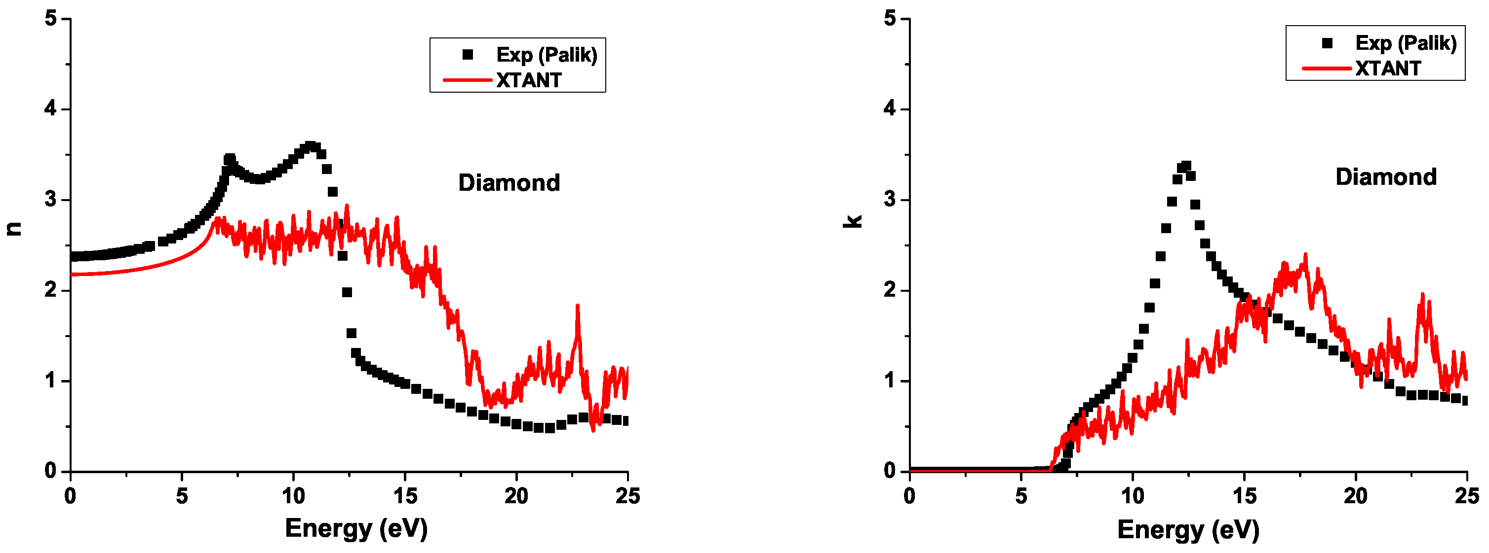
The
and
as functions of photon energy were calculated with XTANT for equilibrium diamond. They are shown in
Figure 1. Comparison with the available experimental [
22] and DFT data [
23] shows discrepancies, e.g., the main peak is missing in the XTANT simulation. This is due to the limited accuracy of the (nearest-neighbour) tight-binding method which we apply here. In particular, it does not describe properly high-lying states in the conduction band and possible resonances. However, the agreement at energies below
eV is reasonably good. As we will see later, it is sufficient for the description of pump-probe experiments with optical probe pulses.
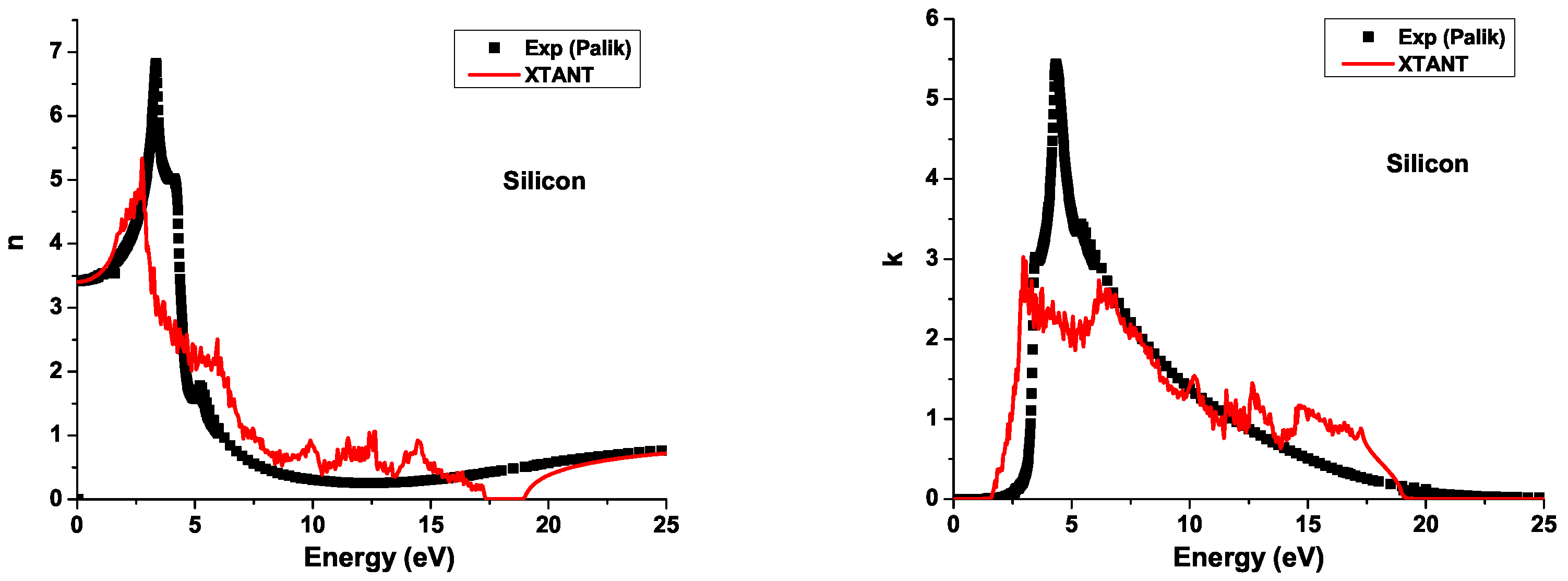
The same comparison was made for silicon, and the same sort of discrepancy was found (
Figure 2). As band gap in silicon is narrower than in diamond, the limiting energy, under which the agreement of data and our simulations is achieved, is at <2 eV. As the later comparison with experimental data will show, this is still sufficient for calculations of optical properties in the optical wavelength regime. Although the accuracy of tight-binding parametrization for a material in a fixed state or phase can, in principle, be improved by incorporating contribution of neighbours up to the third nearest neighbour (shown by Trani et al. in [
20]), such extension is not available for transferable tight-binding scheme applied in XTANT.
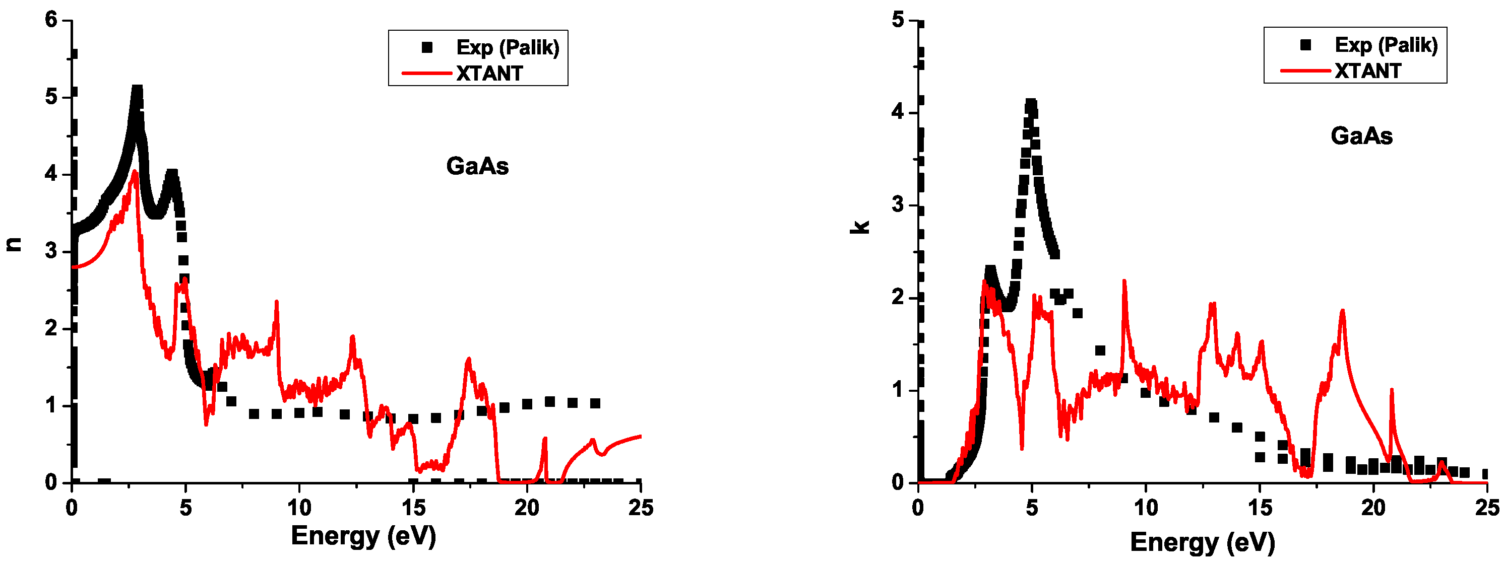
Final comparison was made for GaAs (
Figure 3). The agreement between theory and experiment is worse than in the previous cases due to the complexity of the GaAs band structure.
Finally, let us emphasize that although different transferable TB parameterizations can be found in the literature, we did not explore (and compare) the effect of each specific parametrization on the simulations. This is not straightforward as each parameterization is functionally different and would require a dedicated implementation into the code. The various TB parametrizations arise from the underlying density functional theory (DFT) or Hartree-Fock (HF) calculations, to which the TB parameters are fitted. Consequently, they may produce slightly different cohesive energies or band structures. Thus, one would expect to see an effect of the specific parametrization on the results. However, we are unable to quantify this statement at present; it deserves a separate investigation.
3. Results and Discussion
3.1. Diamond
We begin with a study of transient optical parameters in irradiated diamond. The XTANT model treats only single-photon absorption. Thus, it is limited to photon energies above ∼30 eV and to low FEL fluences. For our simulations we will use photon energy of 50 eV, unless stated otherwise. Such photon energy has been frequently used for experiments at various FEL facilities, for instance, at FLASH [
24,
25], or at FERMI [
26].
We perform a set of simulations with FEL pulses of 50 eV photon energy, Gaussian temporal profile and duration of 90 fs FWHM for different absorbed doses:
eV/atom,
eV/atom, and
eV/atom. The damage threshold dose for diamond is
eV/atom as previously calculated [
12]. For doses above the threshold dose a transition of diamond to graphite can be triggered [
12,
27,
28].
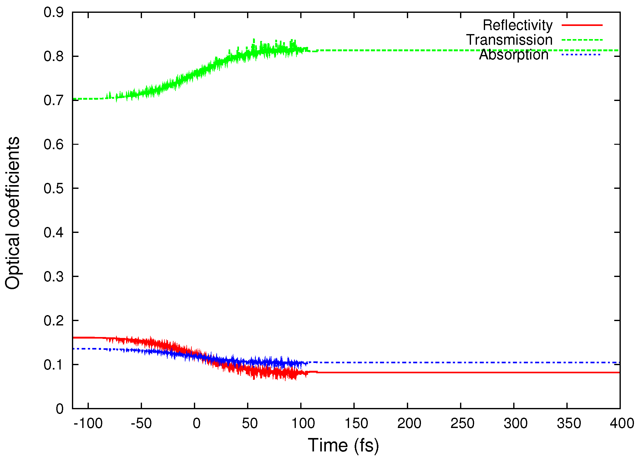
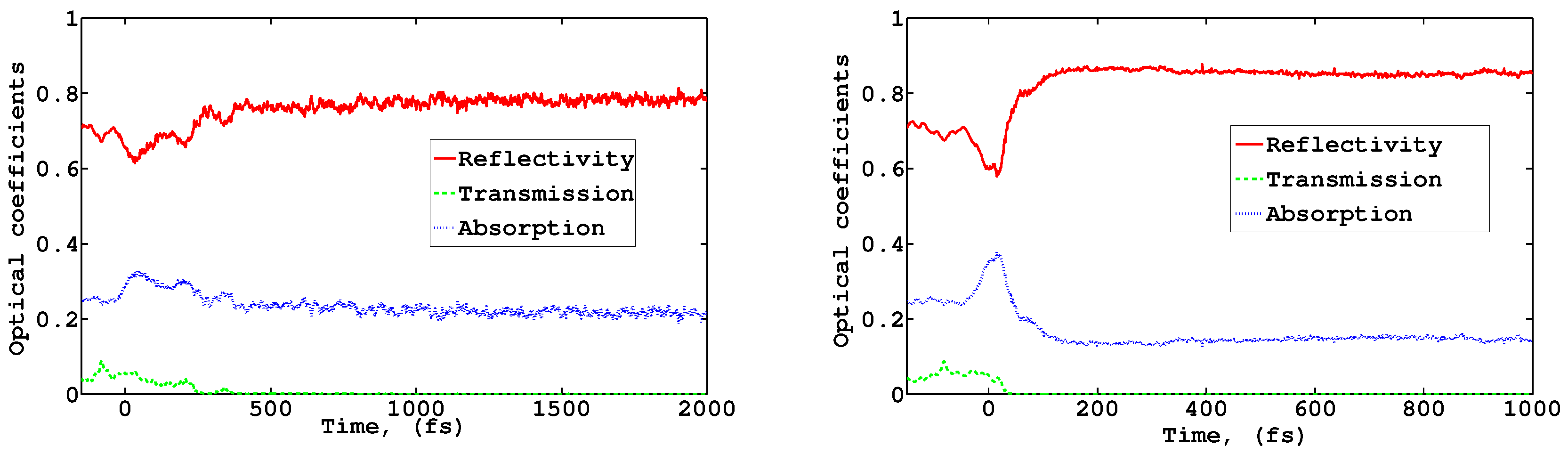
In
Figure 4 time-dependent reflectivity, transmission and absorption coefficients are shown for the three absorbed doses. In all cases a characteristic rise of absorption and drop of transmission are observed already during the pulse. In case of the below-threshold dose, the transmission does not decrease to zero, and the reflectivity slightly changes. For doses above the damage threshold, optical transmission decreases in two stages—first, to some intermediate value after ∼100 fs after the pulse maximum (located at 0 fs), and then to zero after additional 100 fs. The reflectivity rises up at those times, respectively. The transient transmission plateau “shortens”, when the absorbed doses become closer to the damage threshold. If the dose is sufficiently high (above the damage threshold), transmission drops to zero rapidly after 100 fs, without any intermediate plateau, see
Figure 4c.
The following physical processes are responsible for the changes of optical properties. At the first stage, diamond absorbs energy from the laser pulse. Transmission coefficient then begins to decrease. This occurs mainly due to the excitation of electrons from the valence to the conduction band, whereas the electron band structure and atomic structure remain practically unaltered during the first ∼50 fs.
Later, if the density of excited electrons overcomes a certain fraction of the total number of valence band electrons (∼1.5% for diamond), the electronic band structure undergoes significant changes, with the most prominent effect of the band gap collapse [
29]. For above-threshold doses, band gap collapse is clearly visible on the time scale of the transmission decrease. However, it can also occur before the final drop of the transmission to zero, because it takes some time for atoms to relax into a new equilibrium state of graphite [
29]. That is reflected by an occurrence of a transient plateau in the transmission curve mentioned above.
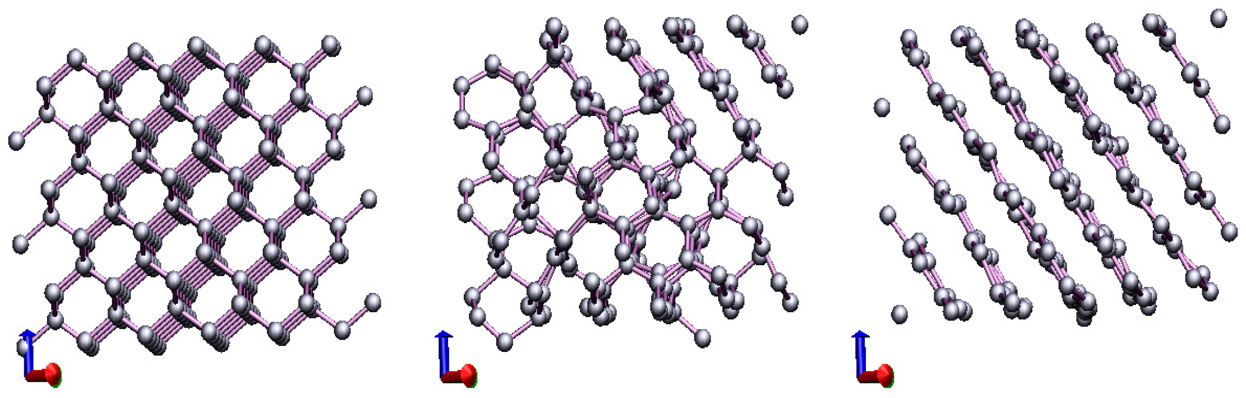
Band gap closure promotes even more electrons to the conduction band, leading to the rapid changes of the potential energy surface. If the change is significant, the sp
bonds in diamond begin to break. We can follow the dynamics of the system by looking at the snapshots of atomic positions at different time steps (
Figure 5). One can see there when the cubic structure and the sp
bonds in diamond are breaking, and when the sp
bonds and individual parallel planes of graphite are forming. Comparison of these figures and the corresponding timescales in
Figure 4 shows that the atomic rearrangement plays a major role in inducing changes of optical coefficients.
We can theoretically study the connection between phase transition and changes of optical coefficients by artificial decoupling of electron excitation and atomic dynamics within the model. For this illustrative example, we “switched off” the transient atomic dynamics, “freezing” the atoms in their equilibrium positions and allowing only the electrons to be excited by an FEL pulse. This modeling scheme tests the correctness of an often-used assumption that the evolution of optical properties can be traced, if only accounting for electron kinetics, while keeping band structure and atomic structure unaffected.
In this “artificial” case, even for an above-threshold dose of
eV/atom, the optical coefficients remain unchanged after the pulse and the completed electron cascading (
Figure 6). This unambiguously shows that the abrupt changes of optical coefficients are the direct outcome of a structural transformation, while the electronic excitation plays there a less important role. Thus, atomic dynamics must be included in models describing the evolution of optical properties in materials under femtosecond X-ray irradiation at doses close or above their damage threshold.
The simulations using supercell with periodic boundary conditions are affected by finite size effects which decrease with increasing number of atoms within the supercell. The oscillations of optical parameters were observed for the case of diamond irradiation at the near-threshold absorbed dose of 0.8 eV/atom. These simulations were performed with 216 atoms in the supercell. In order to check the potential influence of the finite size effect, we performed test calculations with 512 atoms. In this case the amplitude of the oscillations significantly decreased. This would indicate that the finite size effect is responsible for the oscillations. We cannot entirely exclude the possibility of some coherent atomic motion during the system relaxation, however, we cannot resolve it with the current tool and data available.
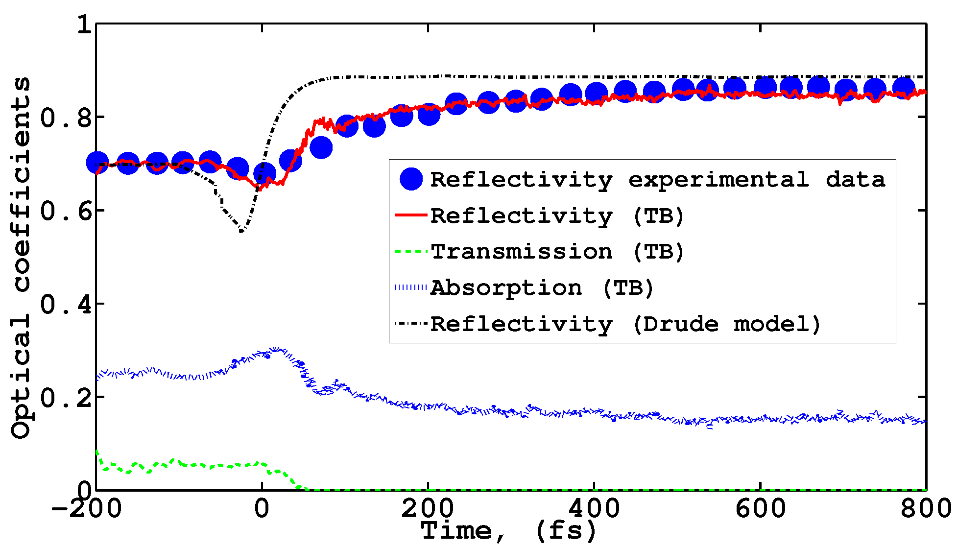
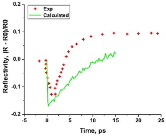
Our simulation results can be compared with the available experimental data. So far, experiments on graphitization have been performed with optical pumping. In the work by Reitze et al. [
30] transient reflectivity of diamond was measured. Optical pump and probe pulses had the same wavelength of 630 nm and duration of 90 fs, and the absorbed dose was 9 times higher than the threshold dose.
As it was mentioned in
Section 3, XTANT code is not able to model optical pumping directly. However, it can use instead soft X-ray pulses. They induce fast cascading of electrons and their fast relaxation. Electronic dynamics in the system becomes then similar to the optical case shortly after the pulse. A good agreement between the measured reflectivity coefficients and our predictions can be seen in
Figure 7. A small discrepancy between predictions and the data during the pulse can be expected due to the reasons presented above. However, the overall agreement of data and predictions is good [
10].
For comparison, we also show the results obtained with the Drude model (with a fixed relaxation time). This model does not take into account interband transitions. As it was discussed above, any model that does not account for both structural and electronic changes within irradiated material will fail to describe the material excitation for doses close to the damage threshold, when atomic dynamics starts to be important [
10].
3.2. Silicon
The XTANT model extended for calculation of optical properties was also applied for silicon [
10]. Amorphization of silicon can occur via thermal and non-thermal melting [
29]. The estimated threshold dose for silicon melting is
eV/atom, when solid silicon transforms into a low-density liquid (LDL). At the dose of
eV/atom full amorphization of silicon occurs (to high-density liquid, HDL) [
13].
Experiment investigating melting of silicon was performed by Sokolowski-Tinten et al. [
31]. It was similar to the experiment carried out by Reitze et al. for diamond. An optical pulse with 625 nm wavelength was used there.
To model this experiment, we again used soft X-ray photon energy (50 eV) for the pump pulse and 625 nm wavelength for the probe pulse.
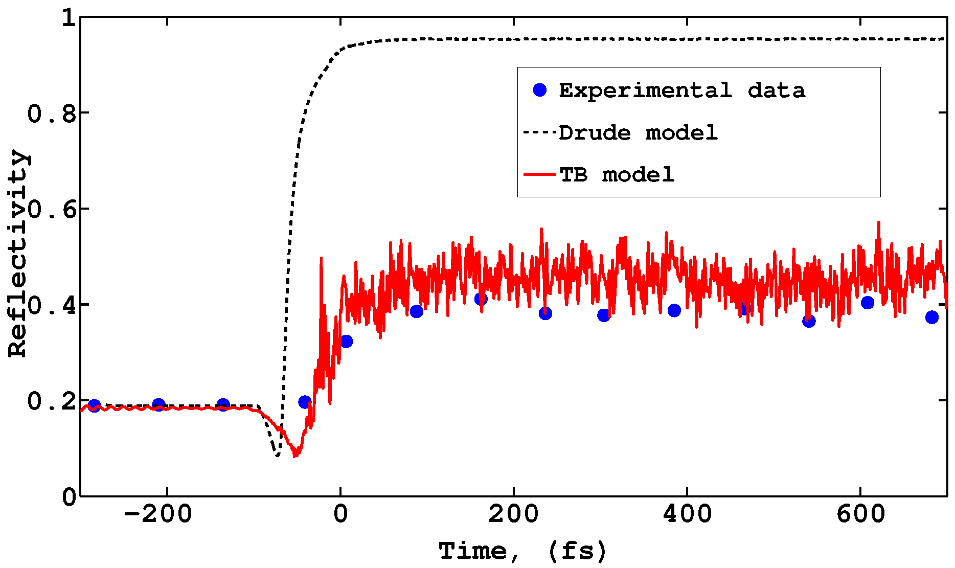
Figure 8 shows optical properties of silicon at the absorbed dose of
eV/atom (above the damage threshold). A characteristic drop of transmission and an increase of reflectivity were predicted by the simulation. The results for the reflectivity were found to be in reasonably good agreement with the experiment.
In contrast to diamond, the increase of reflectivity in silicon is not so rapid. It takes a significantly longer time until it saturates, i.e., 500–600 fs after irradiation. This is the consequence of both non-thermal and thermal processes contributing to silicon amorphization. Shortly after the pulse, the non-thermal melting of the material starts and reflectivity decreases. Afterwards, the reflectivity overshoots its initial value. The dose of
eV/atom is not sufficient to amorphize silicon purely non-thermally, i.e., within a few hundreds of femtoseconds. Heating of atoms by electron-phonon coupling is necessary to accomplish the transition. This usually takes up to a few picoseconds [
29].
During the material heating, its band gap starts to shrink and finally collapses, indicating a phase transition to a semi-metallic state [
13]. This finding has been confirmed by the detailed simulation with XTANT in [
13].
We observe in the simulations that thermal and non-thermal phase transitions can be decoupled if atoms are irradiated at a low dose (slightly above the LDL threshold), and at a very high dose (above HDL threshold). In the first case thermal melting has predominant contribution. In the latter case non-thermal melting prevails.
In
Figure 9 the examples for doses of 0.66 eV/atom and 1.78 eV/atom are shown, correspondingly. One can see that at the lower dose the reflectivity saturates after 1 picosecond (as thermal melting then dominates), while for high dose the saturation appears quickly (as non-thermal melting then dominates), within ∼300 fs. Also, at the dose of
eV/atom the transmission strongly decreases almost immediately after the pulse, while at the dose of
eV/atom it is still non-zero until approximately 400 fs.
This again demonstrates that the optical properties are strongly linked to the atomic structure. For the non-thermal melting, the timescales of the abrupt changes of the optical properties coincide with the timescale of the phase transition. In case of thermal melting, the changes of atomic structure are triggered by the increasing atomic temperature on ps timescales. The timescale of atomic heating, i.e., electron-lattice thermalization time, is, in turn, governed by the electron-phonon coupling. As the optical properties indicate the thermally induced changes of atomic structure, by measuring those properties with a pump-probe scheme, one can estimate electron-phonon coupling rates in semiconductors.
3.3. Gallium Arsenide
Such estimation has been performed for GaAs in [
32], however, not with the code XTANT. The current version of XTANT cannot treat properly the relaxation of X-ray excited GaAs. This is due to the specific band properties of GaAs which, in particular, imply that the effective masses of electrons and holes differ by a factor of ∼10. As a consequence, there is no fast global thermalization of electrons and holes in both valence and conduction bands [
32]. Instead, electrons and holes thermalize separately within the conduction and the valence band, respectively, at the timescale of a few hundred fs. The equilibration of electron and hole temperatures occurs much later, at ∼10 ps. The XTANT code uses currently the assumption of simultaneous thermalization of electrons and holes. It cannot then be applied in this case.
Optical properties of GaAs were studied experimentally in [
9,
33] with VUV/soft X-ray (40 eV) in [
33], and with X-rays (800 eV) in [
9]. The absorbed doses were not sufficient to induce neither non-thermal nor thermal melting.
X-ray photoabsorption triggers secondary electron cascading and production of electron-hole pairs. As soon as the energetic photoelectrons appear, also electron-lattice energy exchange starts. This process lasts for a few picoseconds. Due to the atomic heating, the band gap shrinks, as discussed above.
Including the temperature dependence of the band gap into a two-temperature model (combined with an extended Drude-model), and fitting the model to the experimental data, allowed us to extract the electron-lattice thermalization time in FEL-excited GaAs [
32]. Since the excitation level here is low, we expected the Drude model to be applicable. However, it was not the case. Only after the Drude model was extended to include the effects of: (i) interband transitions, and (ii) the thermally-induced band gap shrinkage, it could reproduce the overshooting effect.
It should also be mentioned that radiative electron-hole recombination time is on the order of 100 ns [
34], thus, it does not give an additional contribution to the optical properties on the considered timescales.
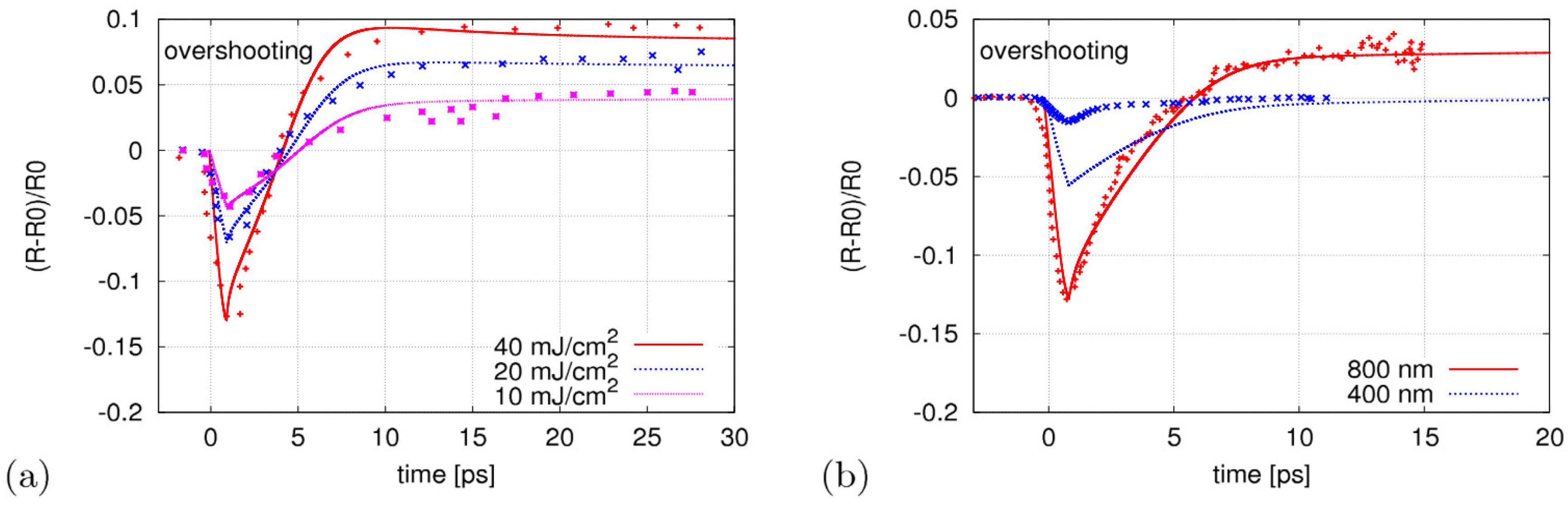
Both experimental results and theory predictions show reflectivity overshooting (
Figure 10). This specific effect appears only if the energy of probe photon is comparable with the band gap width, which makes the optical coefficients to be very sensitive to the changes of the band gap width. For probe-photon energies far above the band gap, this effect is not observable, see the case of 400 nm probe in
Figure 10.
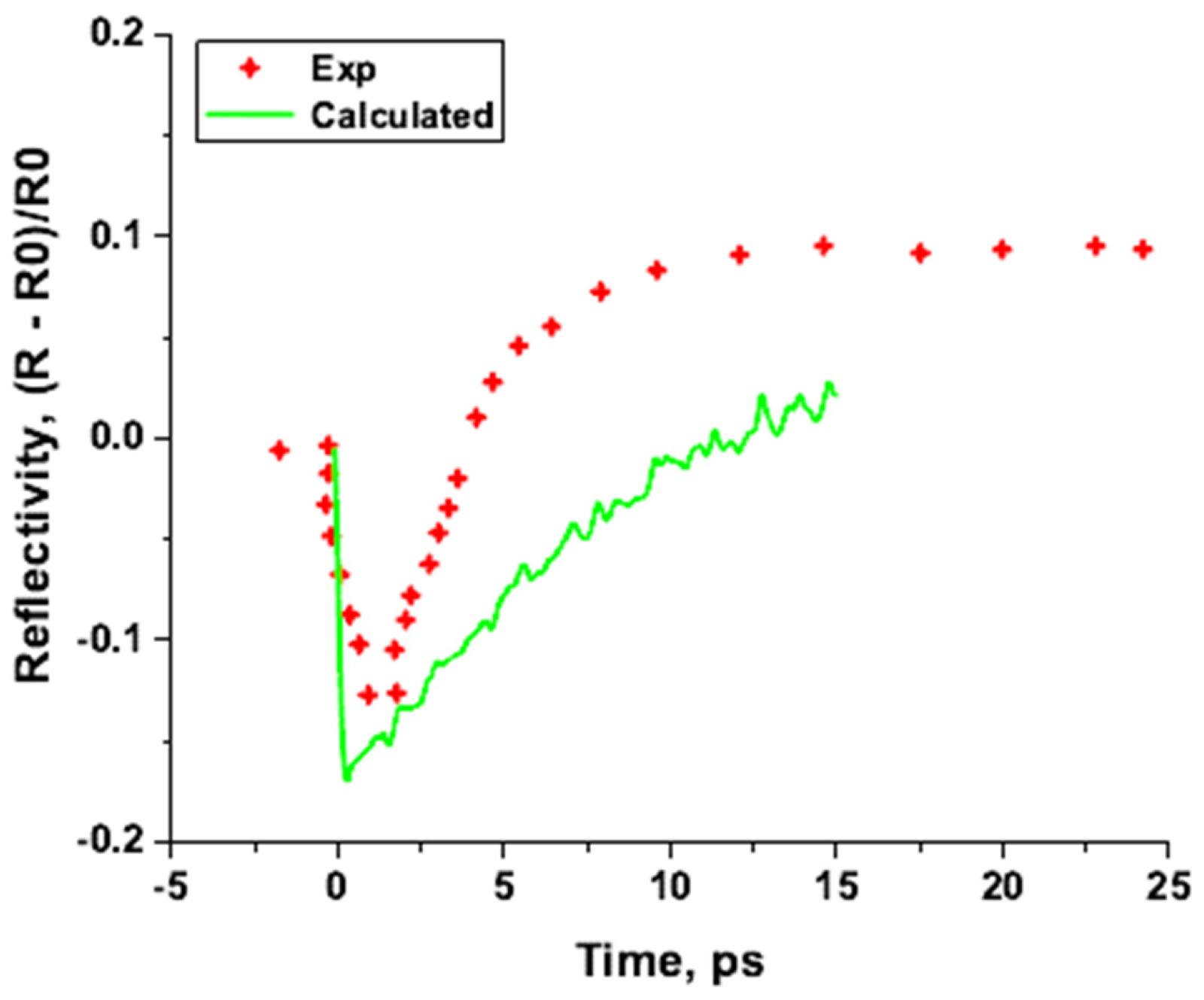
For comparison, we show the reflectivity change obtained with XTANT, assuming a fast global thermalization of carriers between valence and conduction bands (at a timescale of a few hundred fs) at 800 eV FEL pump photon energy and 40 mJ/cm
pulse fluence (
Figure 11). As expected, the predictions are in a clear disagreement with the experimental data. This indicates that a modification of XTANT, going beyond the assumption of fast global equilibration, is required to properly model GaAs. This is a topic of our on-going investigation. Note that for Si and diamond the effective masses of carriers in the conduction and valence band are comparable, therefore, the approximation of the unified Fermi-Dirac distribution for both bands holds already within a few femtoseconds after their irradiation [
10].
Since the band gap width is a function of the lattice temperature, the theoretical and experimental data on reflectivity can be used to extract the electron-phonon thermalization time or the electron-phonon coupling parameter. In case of GaAs irradiated with X-rays below the melting threshold, we extracted the electron-lattice thermalization time from the data and found it to be in the order of 2–3 ps.
This technique can also be applied for other narrow band gap semiconductors. Moreover, the already existing data exhibiting overshooting effects can be reanalized to extract the data on electron-phonon thermalization times. Thus, the pump-probe technique used in femtosecond laser experiments has a potential to study electron-phonon coupling parameters in semiconductors with femtosecond resolution.
4. Conclusions
In this paper we discussed the application of transient optical properties for diagnostics of electronic and structural transitions within semiconductors irradiated with femtosecond laser pulses.
We showed that our in-house developed code XTANT can describe the evolution of the optical properties in irradiated materials both in case of thermal or non-thermal phase transitions. The results of the simulation were found to be in good agreement with the available experimental data. Although the code is designed for X-ray irradiation, it could also describe data from optical experiments with a good accuracy.
Our simulations indicate that structural transitions in semiconductors have a major impact on their optical properties, while the pure electronic excitation plays comparatively a minor role. Still, as it is sensitive to the irradiation, it has been successfully used for non-destructive pulse diagnostics [
2,
3] during FEL experiments.
Pump-probe experiments also allow us to extract information on the electron-phonon coupling in semiconductors. This was demonstrated by the example of GaAs, where the experimentally measured reflectivity overshooting enabled estimation of the electron-lattice thermalization time ∼2–3 ps. similar scheme can be applied to other narrow-band-gap semiconductors.


