Article

A Self-Testing Platform with a Foreground Digital Calibration Technique for SAR ADCs

1
The Department of Electrical Engineering, National Cheng Kung University, Tainan 701, Taiwan
2
The Department of Electrical Engineering, National Taipei University, Taipei, 23741, Taiwan
3
The Department of Computer Science and Information Engineering, Nanhua University, Chiayi 62249, Taiwan
*
Author to whom correspondence should be addressed.
Appl. Sci. 2016, 6(8), 217; https://doi.org/10.3390/app6080217
Submission received: 29 May 2016 / Revised: 24 July 2016 / Accepted: 26 July 2016 / Published: 29 July 2016

Abstract

:
This study presents a self-testing platform with a foreground digital calibration technique for successive approximation register (SAR) analog-to-digital converters (ADCs). A high-accuracy digital-to-analog converter (DAC) with digital control is used for the proposed self-testing platform to generate the sinusoidal test signal. This signal is then implemented using an Arduino board, and the clock signal is generated to test the ADCs. In addition, fast Fourier transform and recursive discrete Fourier transform (RDFT) processors are adopted for dynamic performance evaluation and calibration of the ADCs. The third harmonic distortion caused by the non-linearity of the track-and-hold circuit, the mismatch of the DAC capacitor array, and the direct current (DC) offset of the comparator can be calculated using the processors to improve the ADC performance. The advantages of the proposed platform include its low cost, high integration, and no need for an extra analogy compensation circuit to deal with calibration. In this work a 12 bit SAR ADC and an RDFT processor are used in the Taiwan Semiconductor Manufacturing Co., Ltd. (TSMC) 0.18 μm standard complementary metal–oxide–semiconductor (CMOS) process with a sampling rate of 18.75 kS/s to validate the proposed method. The measurement results show that the signal-to-noise and distortion ratio is 55.07 dB before calibration and 61.35 dB after calibration.

Graphical Abstract

1. Introduction

An analog-to-digital converter (ADC) is an important component in various areas, such as communication and biomedical systems, among others. The performance limitations of the ADCs are mainly dominated by the static and dynamic non-linearity effects, which cause the harmonic distortion in the output power spectrum. These non-linearities slightly deteriorate the overall system performance, and also increase the sensitivity to the process variation and system interface noise because of the technology scaling into the nano-scale region. A calibration method is thus essential to ensure system quality [1,2]. The successive approximation register (SAR) analog-to-digital converter (ADC) has the advantages of medium speed conversion and medium to high resolution. It is therefore very suitable for biomedical and communication systems. With regard to the implementation of most SAR ADCs, the performance should be maintained by the internal circuits, including the track-and-hold (T/H) circuit, the DAC capacitor array, and the comparator circuit. However, the non-linearity of the internal circuits always limits the performance of the ADCs. This is the reason why a calibration method is required to overcome this problem. In this paper we focus on the digital calibration method. For example, the lookup table or the state-space technique is a common calibration method for ADC error correction [3]. The correction in this approach is based on a table that uses pre-calculated values or the slope of the input signal. However, the drawback of this method is the requirement of a large memory size, thus consuming more areas. An equalization-based digitally calibrated method is proposed in Reference [4]. The advantage of this is the reduction of both the ADC testing time and the convergence time. In addition, this paper utilizes the least mean squares (LMS) algorithm to correct and calibrate the ADC error, similar to that in Reference [5].
An internal redundancy dithering (IRD) technique is reported in Reference [6]. The IRD method based on bit-weight calibration employs a pseudorandom bit sequence to determine the threshold values. The method utilizes the LMS algorithm to calibrate the SAR ADC error. However, the main drawback of the approaches in References [5,6] is that a high resolution ADC is required, which is impractical in actual implementation. A fast-Fourier transform (FFT)-based calibration method for pipelined ADC is reported to calibrate the capacitor mismatch and non-linearity error of the operational amplifier (OPAMP) [7]. However, the shortcoming of the FFT process is the consumption of more power because all frequency bins should be computed during the operation mode. Juan et al. proposed an RDFT-based calibration algorithm to overcome this problem [8], because the RDFT processor has the advantages of variable transform length, lower complexity, and less hardware cost.
In this paper, we present a self-testing platform based on previous works [7,8] to measure the ADC performance using the proposed testing stimulus and compensate for the error using a simplified digital calibration algorithm. A 12 bit SAR ADC and an RDFT processor are implemented in the TSMC 0.18 μm to verify the proposed platform. The output is analyzed using MATLAB (version 7.6.0.324 (R2008a), The MathWorks, Natick, MA, USA, 2008), including the performance calculation and ADC calibration.

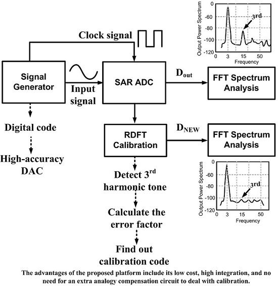
2. Proposed Self-Test Platform

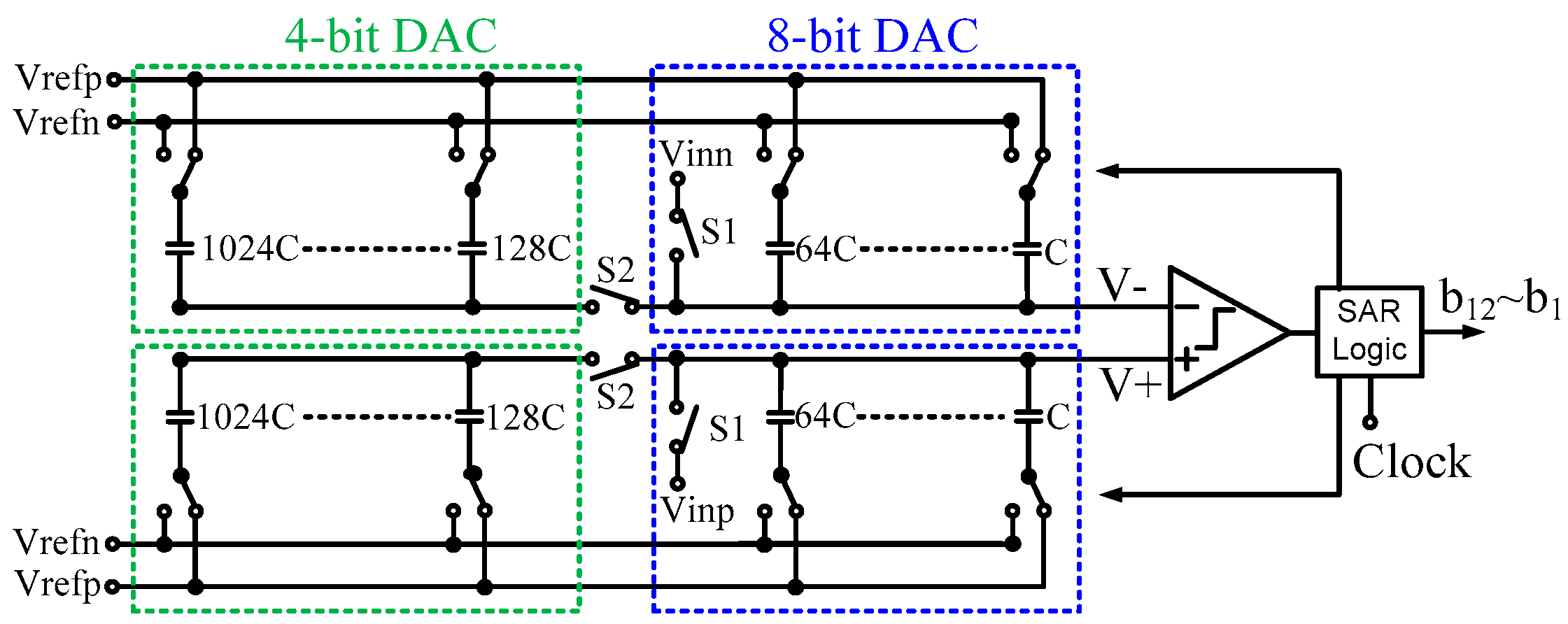
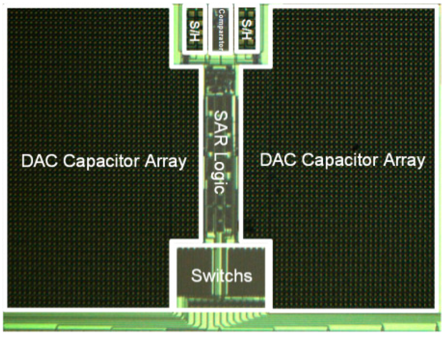
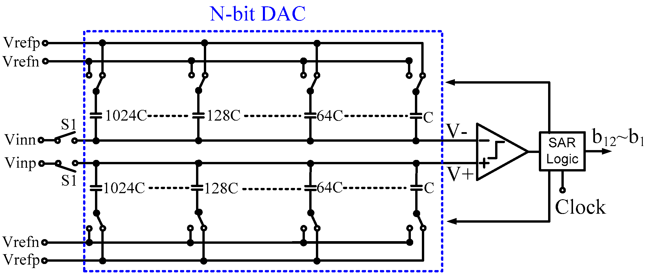
2.1. Conventional SAR ADC Architecture

The basic block of the traditional SAR ADC includes a track-and-hold circuit (T/H), an N-bit DAC capacitor array, a comparator circuit, and a SAR controller (Figure 1). The SAR ADC generally uses a binary-weighted method to implement the circuit [9]. According to the results for the switching capacitor array, the digital output signal can be obtained as Logical High (“1”) or Logical Low (“0”). In addition, some biomedical applications require an adaptive resolution using a multi-switch operated in 8 bit or 12 bit mode [9]. However, the non-linearity of the multi-switch in the T/H circuit will limit the SAR ADC performance. The proposed calibration method also has the capability of eliminating the non-linearity and enhancing the performance of the multi-mode SAR ADC. Figure 2 depicts the multi-mode SAR ADC structure. In this, switch S2 is applied to control the two operation modes, namely the 8 bit and 12 bit modes. The bootstrapped switch is also adopted to provide a small on-resistance with a constant value and better linearity.

2.2. Proposed Calibration Method

A previous work [8] derived the proposed calibration formula using the FFT and a cosine wave input signal. The third harmonic distortion value a3 can be detected by an RDFT processor. The error factor Δn can be further calculated for the calibration. In addition, the calibration code was only used for the first-time test to reduce the complexity. This calibration method can not only compensate for the error caused by the capacitor mismatch and DC offset in the traditional ADC but it can also be applied to calibrate the T/H circuit in the multi-mode SAR ADC (Figure 2).
The main calibration equation can be written as follows:
a 3 = 20 log ( A × Δ n × 1.696 × C n 2048 + 1.696 × V os ) ,
where A is the amplitude of the cosine wave, Cn is the value of each capacitor ratio, Δn is the error factor of each capacitor mismatch, and Vos is the DC offset. The DC offset voltage of the comparator circuit can be expressed as:
V os = ( V ov 2 Δ R D R D ) 2 + ( V ov 2 Δ ( W L ) ( W L ) ) 2 + ( Δ V t ) 2 ,
where Vov, W/L, and Vt are the overdrive voltage, transistor size, and threshold voltage of the differential pair, respectively. According to Equation (2), the threshold voltage is a static offset, which does not affect the dynamic performance of the ADC. Meanwhile, both the overdrive voltage and transistor size will degrade the ADC performance. Some approaches have been used to overcome this problem and improve the DC offset, such as reducing the overdrive voltage or increasing the comparator size. However, the drawbacks of these methods are the decrease in the comparison speed and higher power consumption, respectively. Therefore, the problem can be overcome using the RDFT processor in a system-on-a-chip to calibrate the ADC error [8]. Generally, if a DC offset value will be very small, it will not affect the performance of the ADC. However, if a DC offset is a bigger value, the performance of the ADC will be decreased. Figure 3 shows the MATLAB simulation results with different DC offset variations.
The calibration equation can be rewritten as (3). Here, we assume that A = 1 V, and the DC offset (Vos) is 2 mV:
Δ n = ( 10 a 3 0.0033 ) × 2048 1 × 1.696 × C n , n = 11 ~ 0 ,
In addition, the input signal of the RDFT processor can be a sine or cosine wave signal. Therefore, the power spectra of the RDFT have real (Re) and imaginary (Im) part energies, respectively, in which a3 is equal to:
20 log ( Re ) 2 + ( Im ) 2 ,
The value of a3 can be substituted as the real and imaginary parts. Therefore, Equation (3) can be further simplified as follows:
Δ n = ( 10 1 2 log ( Re ) 2 + ( Im ) 2 0.0033 ) × 2048 1 × 1.696 × C n , n = 11 ~ 0 ,
where Cn is the value of each capacitor array. Equation (5) can be used to evaluate the error factor (Δn). The final correction code utilized to compensate for the error is further obtained as follows:
D new = B i t 12 × 2 11 × ( 2 ± Δ 12 ) + B i t 11 × 2 10 × ( 2 ± Δ 11 ) + + B i t 1 × 2 0 ,
The third harmonic distortion can be significantly reduced when the compensation is finished. The ADC performance can then be improved. In addition, the residue errors are not only compensated, but also corrected by fine-tuning.

2.3. MATLAB Verification

MATLAB is used to simulate and verify the proposed self-testing platform technique and calibration method and build the behavior model, which includes the 12 bit SAR ADC, RDFT computation, signal generator, and proposed calibration. In addition, a 1% capacitor mismatch, 2 mV DC offset, thermal noise, sampling jitter and switch nonlinearity are adopted in the 12 bit SAR ADC model to demonstrate the proposed calibration. Generally, the backgate effect of the switch transistor is the main source of its resistance nonlinearity. So, the input-dependent switch transistor can be defined as:
R = 1 μ C ox ( W L ) [ V DD V th ] ,
In this work, the parameters of the sampling switch are determined by the virtual process, so the backgate effect value of this switch transistor is:
R p = 1 86 × 10 6 ( 0.18 ) [ 1.8 ( 0.5 ) ] 0.911 k ,
R n = 1 387 × 0 6 ( 0.18 ) [ 1.8 0.5 ] 0.358 k ,
It is worthily noted that the body effect problem is not considered in this issue. In this work, the switch model given by using the MATLAB Simulink tool is the transmission gate (pmos and nmos) architectures, and then we further determine the switch nonlinearity error according to the virtual CMOS process parameter. After putting these parameters into Equation (7), we can process the performance analysis of the SAR ADC under the conditions of a 1% capacitor mismatch, 2 mV DC offset, thermal noise, sampling jitter and switch nonlinearity error.
Figure 4a shows the simulation result. It can be easily observed that the distortion deteriorates the ADC performance in the simulation result with a 5 Hz input frequency at a sampling rate of 126.26 Hz. Furthermore, the third harmonic distortion tone is −55.29 dB without calibration and −80.97 dB with calibration (Figure 4b). The signal-to-noise and distortion (SNDR) can be improved from 48.32 dB to 65.65 dB, while the effective number of bits (ENOB) is improved from 7.73 bits to 10.61 bits. However, the proposed calibration method cannot compensate for the error of the thermal noise, sampling jitter and sampling switch nonlinearity, which generated the harmonic distortion at the output power spectrum, so the ADC such as SNDR and spurious-free dynamic range (SFDR) cannot achieve the ideal ADC performance. Figure 5 shows the time domain result, and it is clear that the signal can be improved when the proposed calibration method is applied.
Figure 6 shows the simulation result with capacitor mismatch only and analyzes the performance of the ADC before/after calibration. According to the simulation result, the third harmonic distortion tone is −65.59 dB without calibration and −90.81 dB with calibration. The ENOB can be improved from 9.92 bits to 11.11 bits. In addition, Figure 7 shows the simulation result with 2 mV DC offset only and analyzes the performance of the ADC before/after calibration. According to the simulation, the proposed calibration method can reduce the DC offset error and enhance the performance of the ADC.

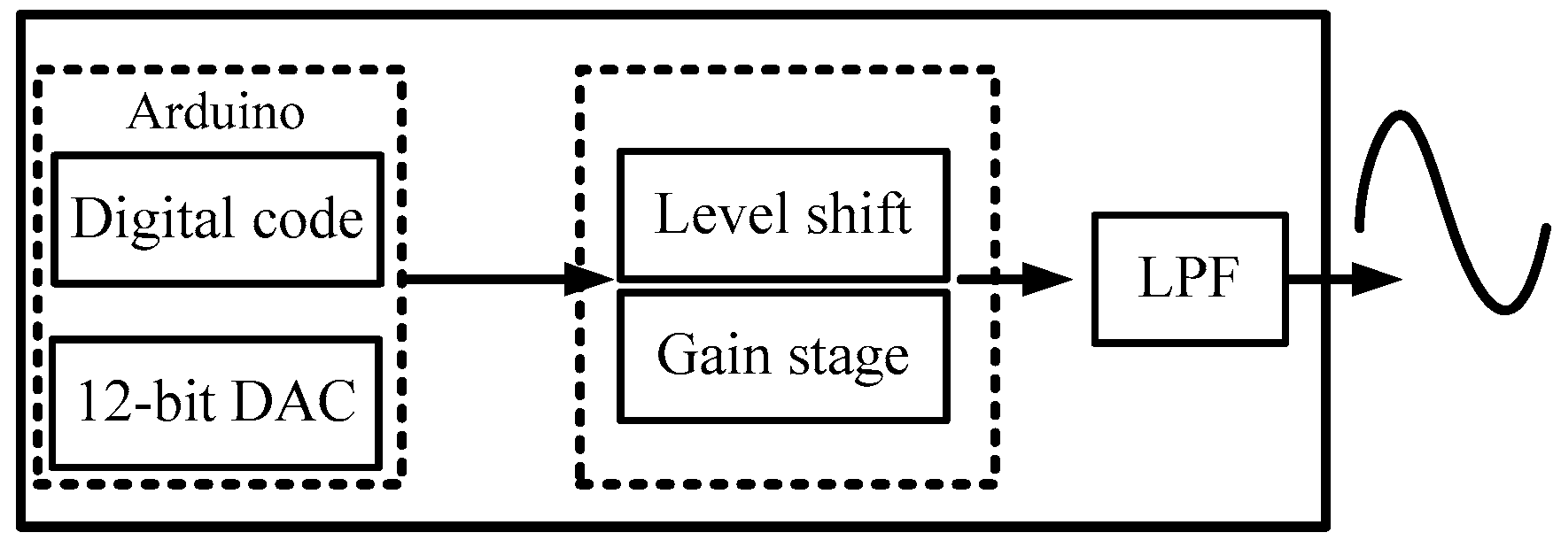
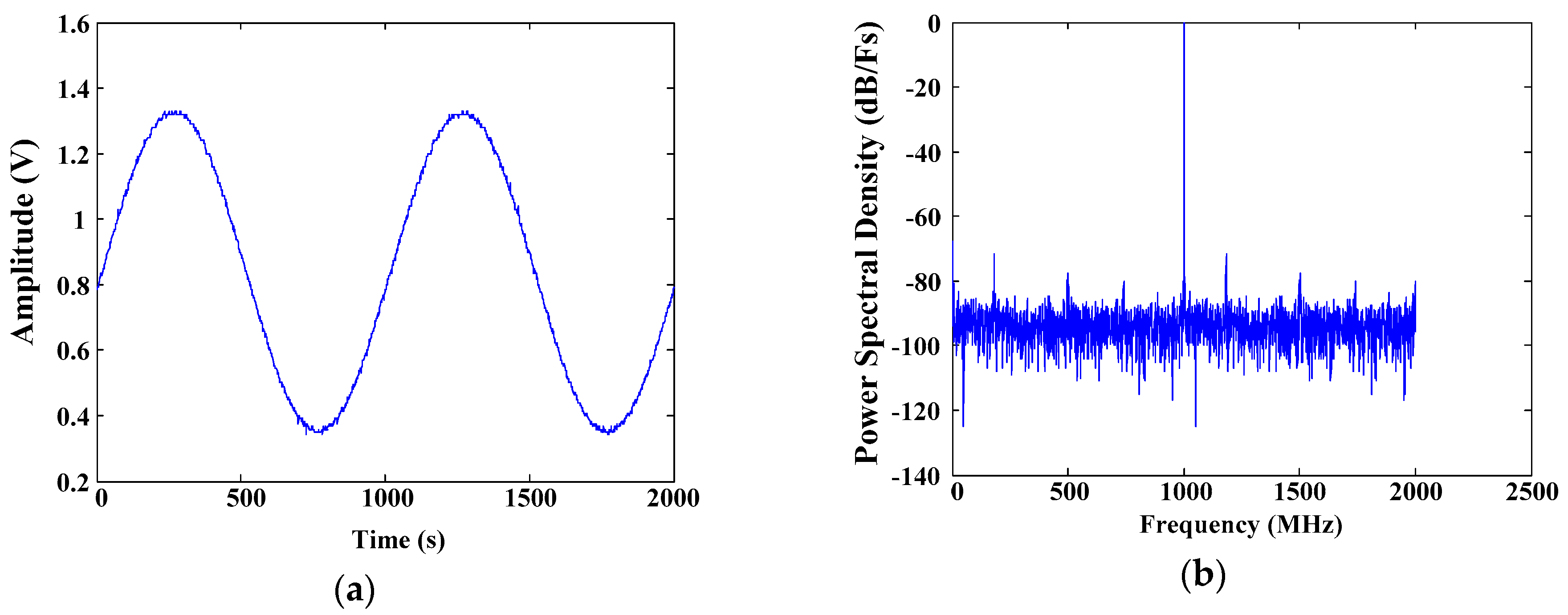
2.4. Testing Stimulus Signal
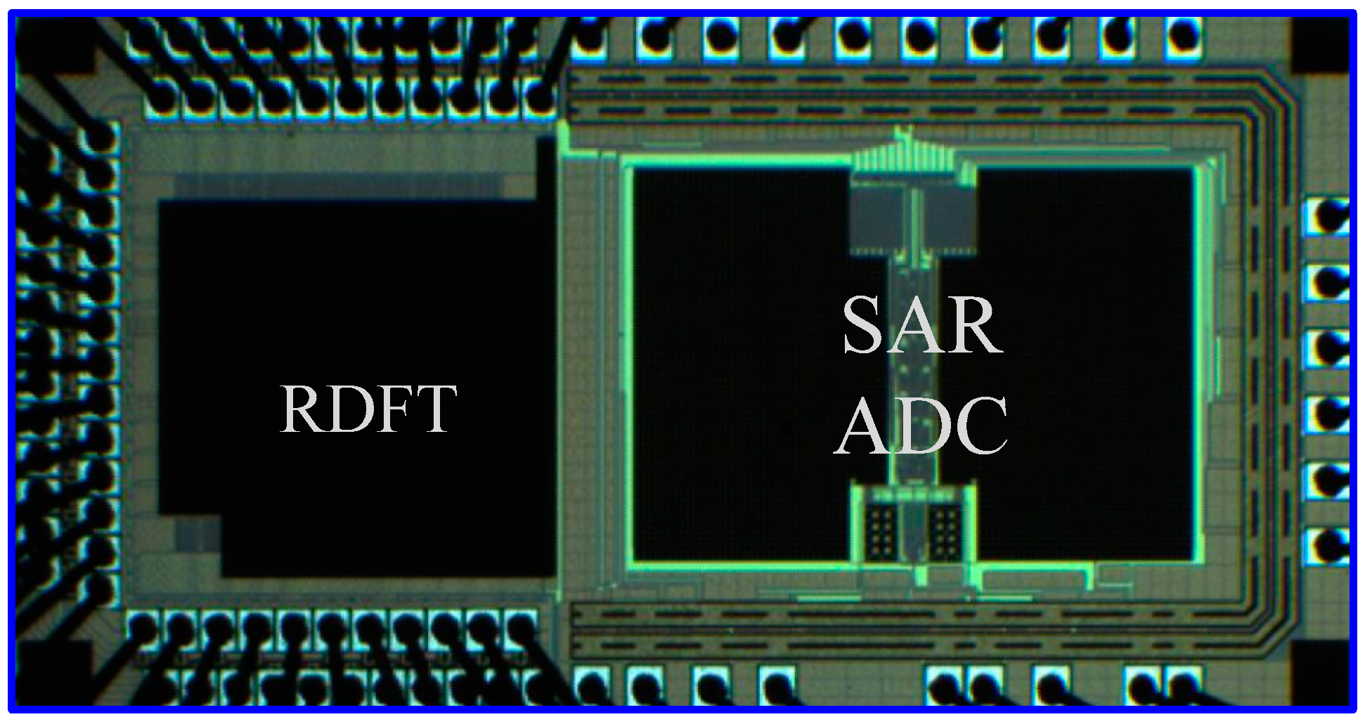
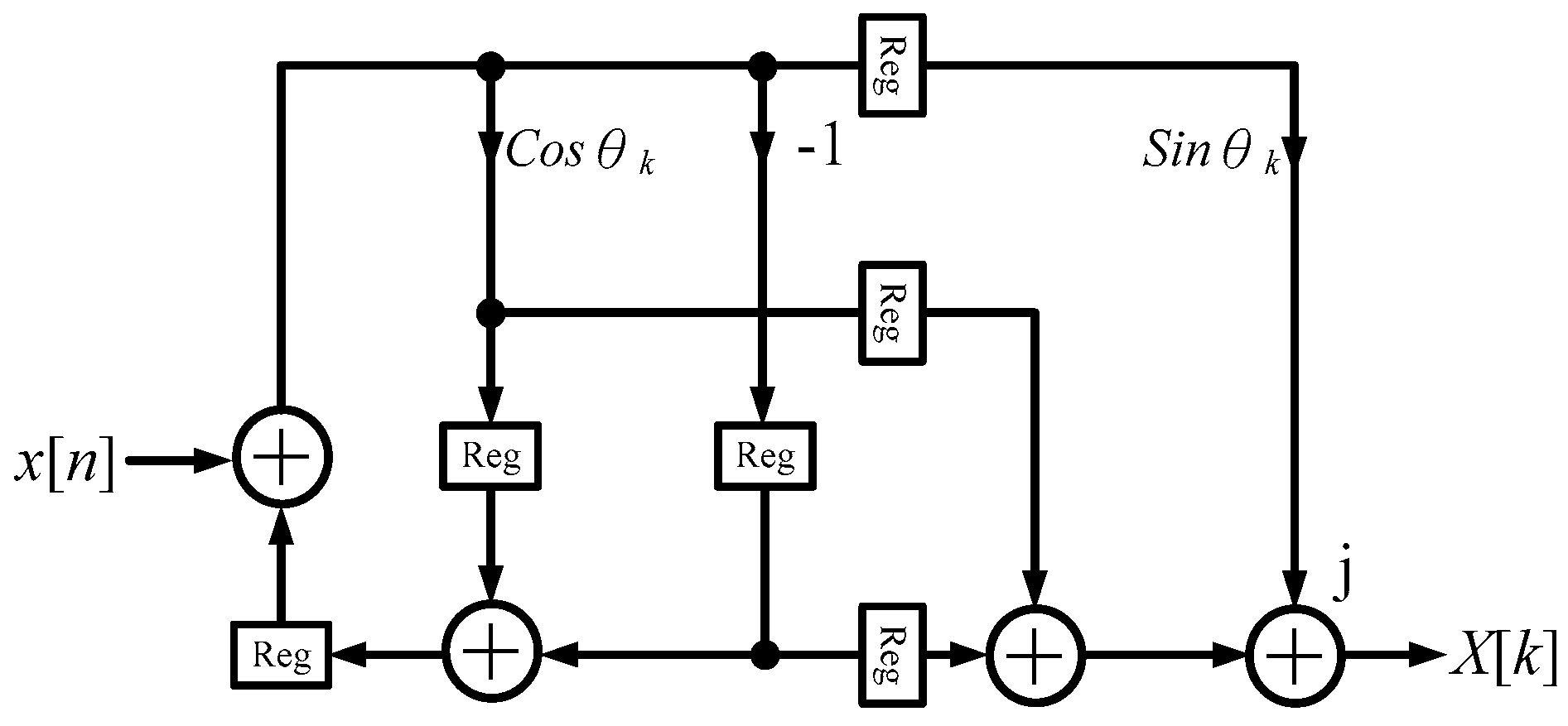
Generally, the dynamic performance of the ADC, including the total harmonic distortion, signal-to-noise ratio, signal-to-noise and distortion ratio (SNDR), and effective number of bits (ENOB), is evaluated by stimulation using the input signal of a sinusoidal waveform and analysis using a digital signal processor [10]. Therefore, a high-accuracy DAC controlled by a digital code in the Arduino board is used to implement the sinusoidal testing signal. Figure 8 shows the basic block of the signal generator. A gain stage and a level shift are employed to adjust the signal amplitude and the required DC level. In addition, a low-pass filter is used to reduce the noise, eliminate the error, and enhance the signal performance. Figure 9 shows the experimental results, which reveal that this signal generator has a spurious dynamic range (SFDR) of 52 dB.
The clock signal is required to control the ADC for most of the ADC testing platform. Figure 10 shows the experimental results of the clock signal, and the root mean square of the jitter is 0.808 ns.

2.5. RDFT Design

Figure 11 shows an RDFT processor structure used to efficiently compute the desired power spectrum density of the signals, including fundamental and third harmonic tones [11]. According to Reference [11], we found that the z-transform formula of the N-point RDFT computation can be defined as follows:
H ( z ) = W N k z 1 1 2 cos ( 2 π k N ) × z 1 + z 2 ,
The coefficients of cos(θk) and 2cos(θk) can be shared to reduce the multiplication of cos(θk) using the same computation; hence, Equation (4) can be written as follows:
H ( z ) = j sin ( θ k ) + ( cos ( θ k ) z 1 ) 1 z 1 ( 2 cos ( θ k ) z 1 ) ,
In the targeted application, the RDFT processor calibration method would have a better performance than the FFT processor because only two frequency bins (i.e., the main and third harmonic tones) should be calculated. Therefore, the computational complexity can be lower than in the FFT processor. In this work, an RDFT processor is implemented in the TSMC 0.18 μm standard CMOS process to execute the calibration under the transform length of 4096 and the world length of 24 bits. Moreover, the computational complexity includes a total of (2N + 2) multiplications and (4N + 2) additions.

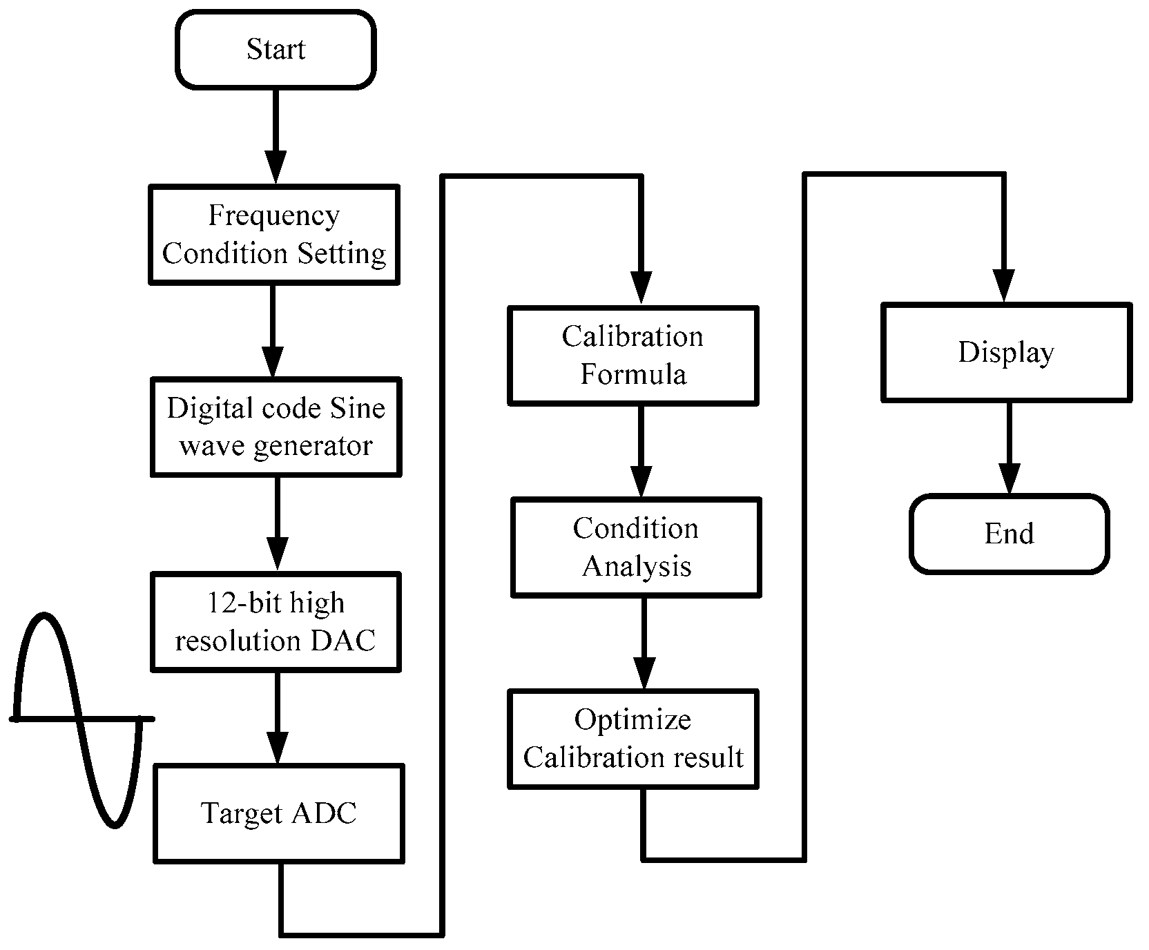
2.6. Processing Flow of the Proposed Self-Testing Platform

Figure 12 shows the processing flow of the self-testing platform method. According to the block diagram, it starts from a sine wave generator with a frequency condition setting, and then a 12 bit DAC output signal is fed into the target SAR ADC. Next, the RDFT processor is used to detect the third harmonic tone and the proposed calibration formula is employed to calculate the error factor. Finally, we can use this error factor to compensate for the ADC error using the re-coding method.

2.7. Proposed Platform Design

The proposed self-testing platform architecture is illustrated in Figure 13. This platform includes a power board, clock generator, sinusoidal waveform generator, and testing chip. In the power board design, the LM317 device is adopted to provide a stable and high-performance supply voltage for the testing platform. We can utilize the logic analyzer or the Arduino board to catch the output data. Finally, the MATLAB tool is adopted to analyze the output signal.

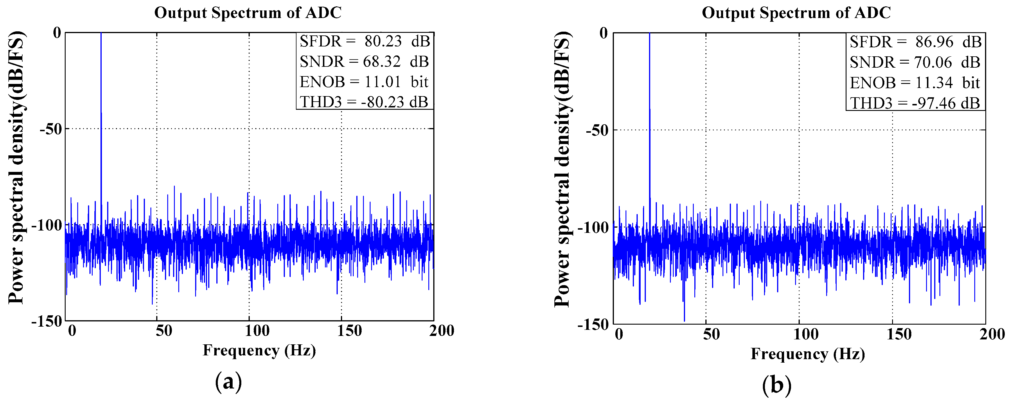
3. Measurement Results

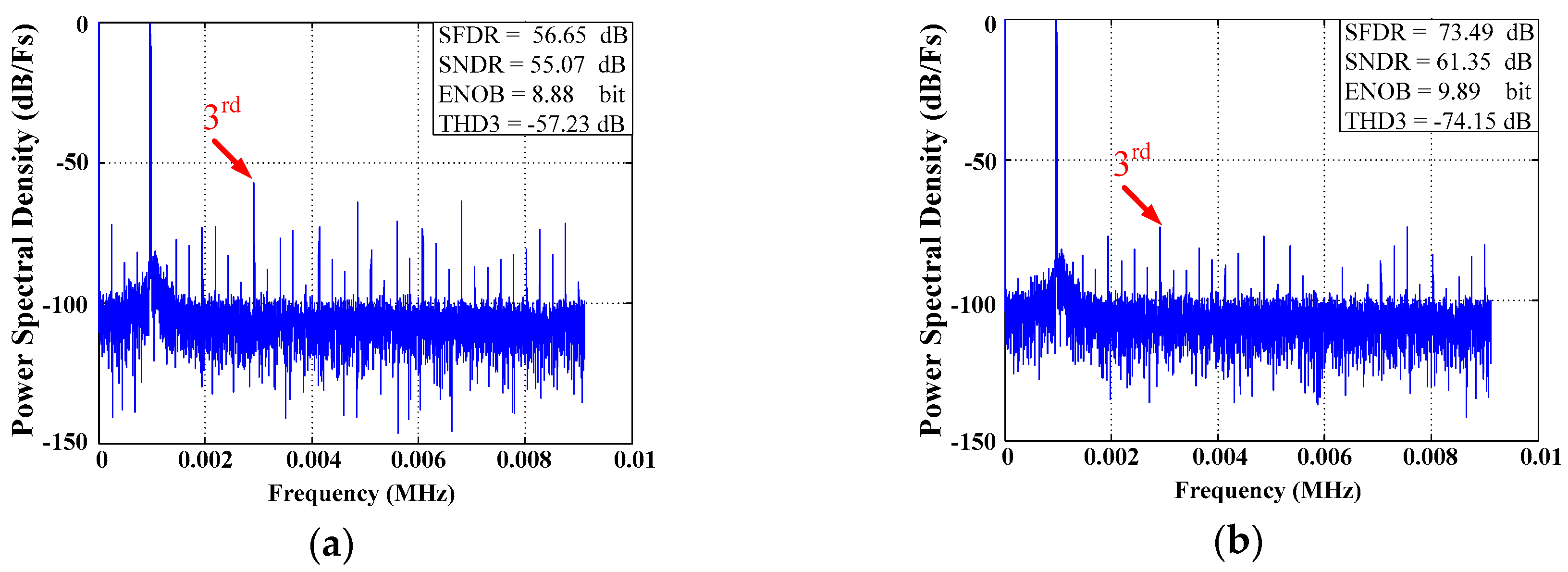
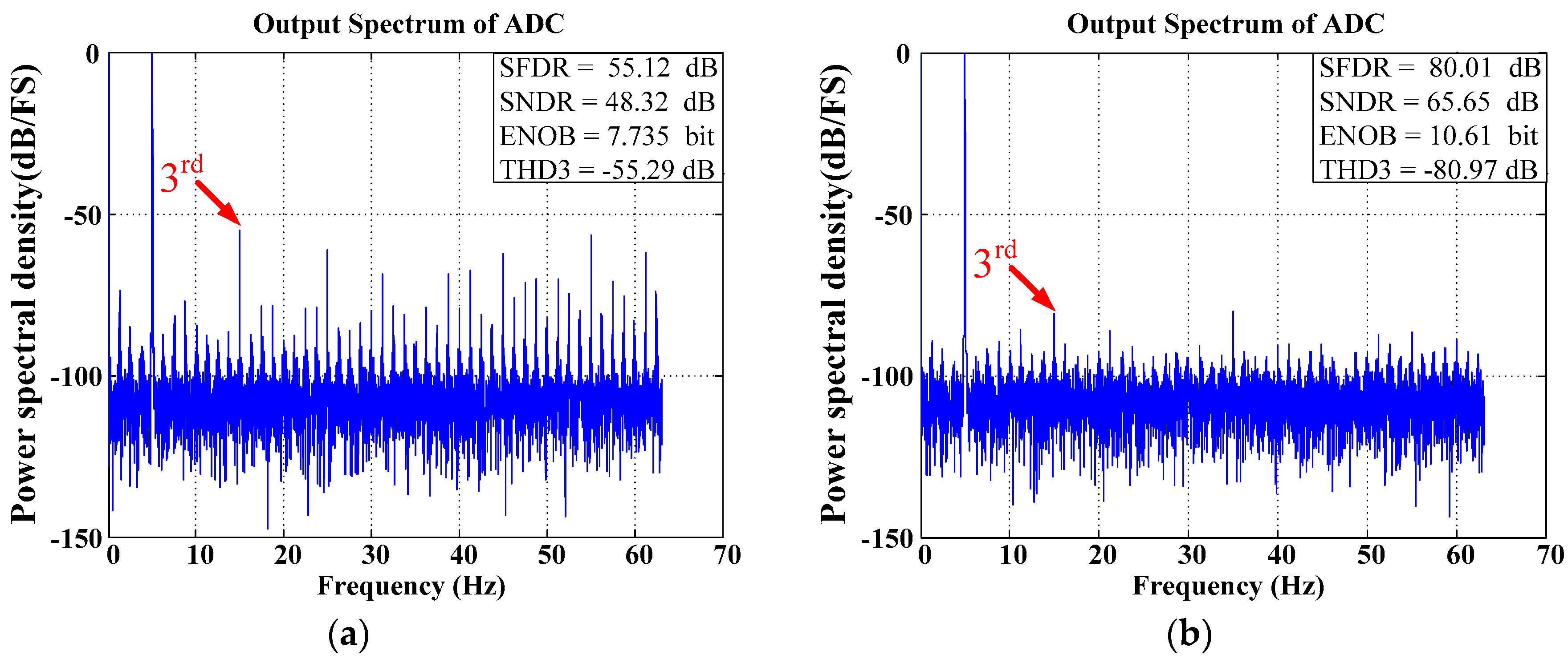
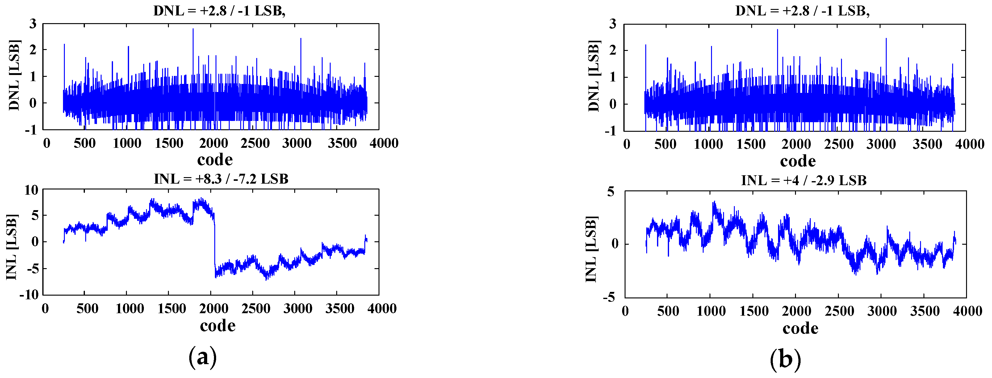
3.1. Multi-Mode SAR ADC

A 12 bit multi-mode SAR ADC is implemented in the 0.18 μm standard CMOS process to demonstrate the proposed idea. The chip microphotograph is shown in Figure 14, in which the core circuits have an area of 1.219 mm × 0.938 mm. Figure 15a,b show the output power spectrum before/after calibration under a 3 kHz and 1 Vp-p input signal with a 125 kHz sampling rate. The third harmonic distortions without and with calibration are −65.53 dB and −78.95 dB, respectively. The SFDR here is 65.39 dB before calibration. The SFDR of 78.80 dB can be achieved after calibration. However, the improvement in SNDR and ENOB is not that significant because the SAR ADC performances are dominated by system noise and tones caused by supply noise and cross-talk, which should be overcome by careful layout.

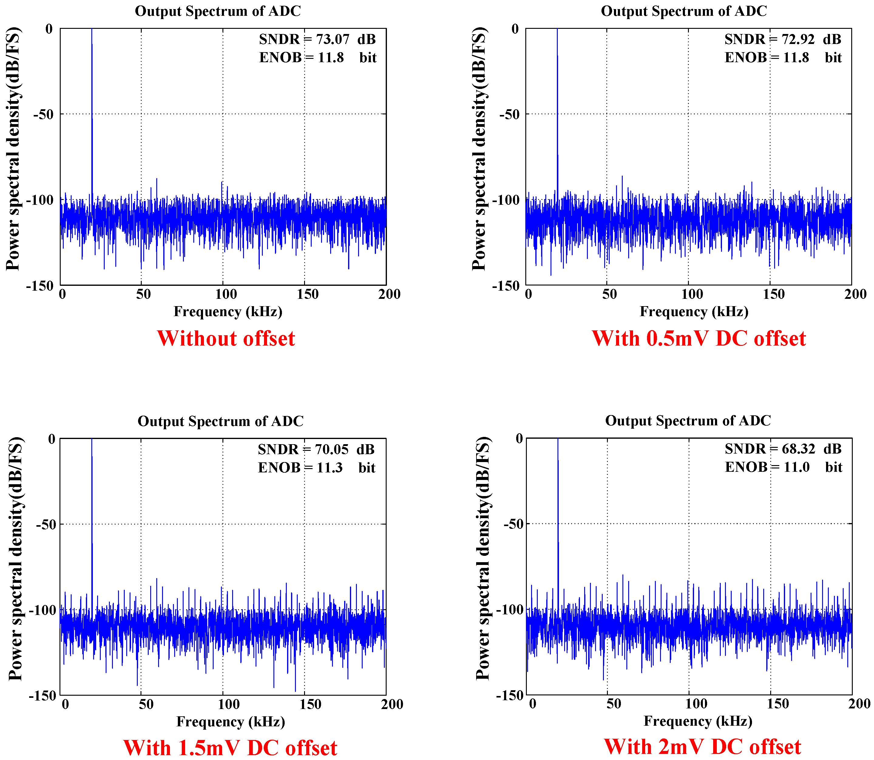
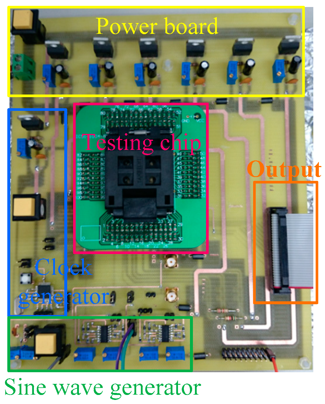
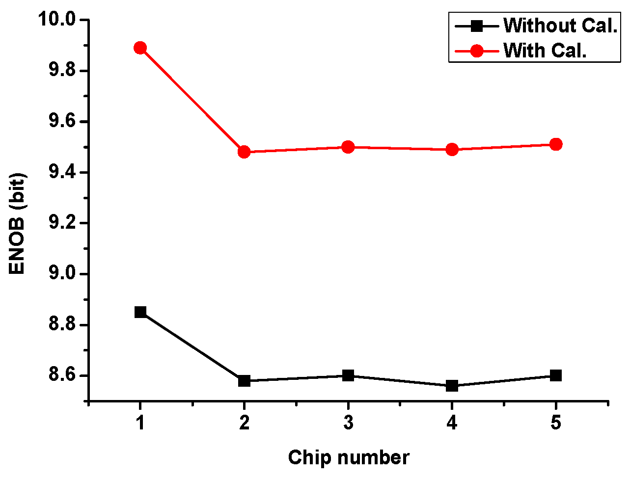
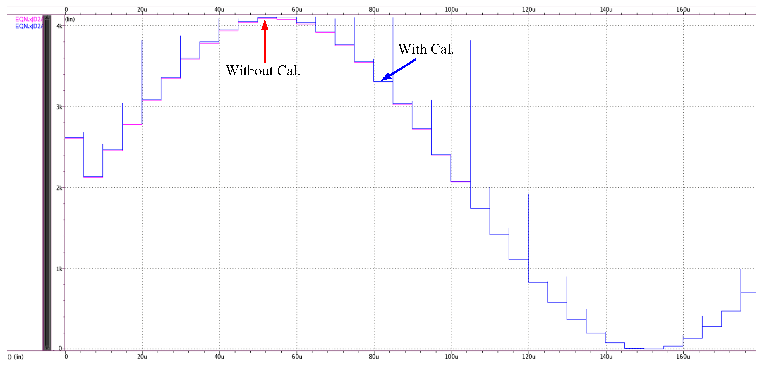
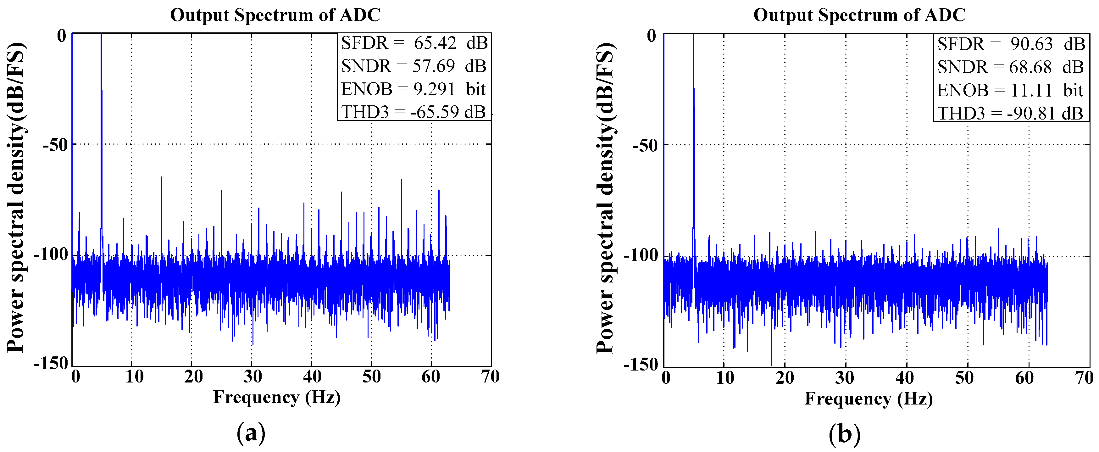
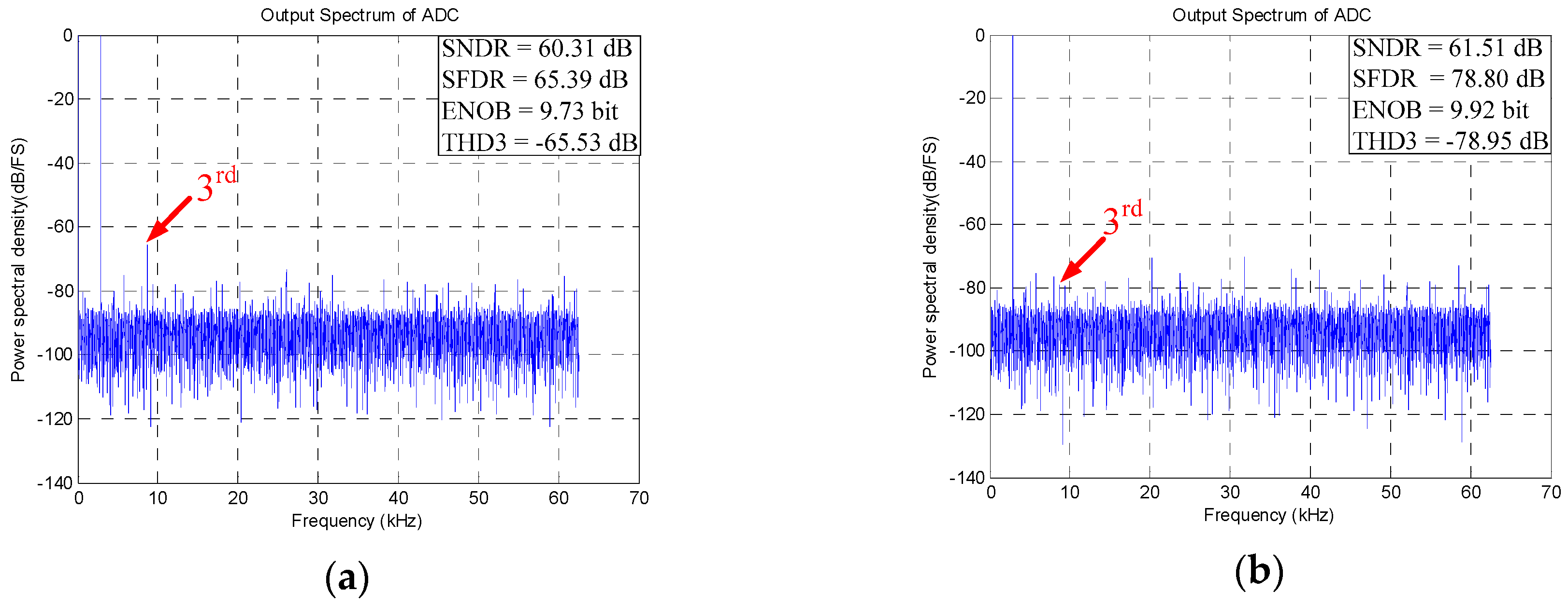
3.2. Proposed Self-Testing Platform

The 12 bit SAR ADC and RDFT processor is implemented in the 0.18 μm standard CMOS process to demonstrate the proposed method. The chip microphotograph is shown in Figure 16, in which the core area is 1.118 mm × 2.13 mm.
Figure 17a,b show the output power spectrum with and without calibration under a 1 kHz and 1 Vp-p input signal with an 18.75 kHz sampling rate. According to the measurement results, the third harmonic distortions without and with calibration are −57.23 dB and −74.15 dB, respectively. The SNDR can be improved from 55.07 dB to 61.35 dB. Figure 18 shows the differential nonlinearity (DNL) and integral nonlinearity (INL) measurement results for this work. The INL is improved from +8.3/−7.2 least significant bit (LSB) to +4/−2.9 LSB. This calibration method enhances INL but not DNL because this method is only adopted using the RDFT processor to evaluate the real radixes, and thus the DNL has no significant change. The calibration procedure is also tested with different testing chips (Figure 19). It is easy to observe that the performance of the ENOB can be enhanced to about 1 bit for different testing chips.
Table 1 compares the proposed method and other state-of-the-art ADCs. Although the proposed method does not have a better performance than that in Reference [12], it still exhibits better power consumption and area improvement. In addition, the performance of the split-capacitive digital-to-analog converter (CDAC) method with 0.9 bit improvement is not as good as that of our proposed method.

4. Conclusion and Discussion

In this paper, a self-testing platform with a digital calibration method for SAR ADC is presented to overcome the non-linearity error of the T/H circuit, the capacitor mismatch of the DAC capacitor array, and the DC offset of the comparator. The proposed platform has the advantages of low cost and high integration without requiring extra analogue circuits or a complex digital calibration algorithm. The testing chip is implemented in the 0.18 μm standard CMOS process. The background signal is analyzed by the MATLAB tool to demonstrate the calibration algorithm and measured performance. According to the measurement results, the ENOB can be improved by 1 bit.

Acknowledgments

The authors would like to thank the Chip Implementation Center of Taiwan and the Ministry of Science and Technology (MOST) of Taiwan under Grants MOST 104-2218-E-006-022 for their support in this study, as well as the CBIC Lab, APSIC Lab, and Hui-Wen Chang in the CWMI Lab.

Author Contributions

Yi-Hsiang Juan, Hong-Yi Huang, Shuenn-Yuh Lee and Ching-Hsing Luo conceived and designed the analog circuit, the proposed calibration method, and the experiments. Shin-Chi Lai and Wen-Ho Juang provided the digital circuit design and analyzed the data. Yi-Hsing Juan and Shuenn-Yun Lee wrote the paper.

Conflicts of Interest

The authors declare no conflict of interest.

References

  1. Zou, X.; Xu, X.; Yao, L.; Lian, Y. A 1-V 450-nW fully integrated programmable biomedical sensor interface chip. IEEE J. Solid-State Circuits. 2009, 44, 1067–1077. [Google Scholar] [CrossRef]
  2. Nakane, H.; Ujiie, R.; Oshima, T.; Yamamoto, T.; Kimura, K.; Okuda, Y.; Tsuiji, K.; Matsuura, T. Afully integrated SAR ADC using digital correction technique for triple-mode mobile transceiver. IEEE J. Solid-State Circuits. 2014, 49, 2503–2514. [Google Scholar] [CrossRef]
  3. Balestrieri, E.; Daponte, P.; Rapuano, S. A state of the art on ADC error compensation methods. IEEE Trans. Instrum. Meas. 1987, 54, 1388–1394. [Google Scholar] [CrossRef]
  4. Chang, H.M.; Lin, K.Y.; Cheng, K.T. Tester-assisted calibration and screening for digitally-calibrated ADCs. IEEE Trans. Circuits Syst. I Reg. Pap. 2011, 58, 2838–2848. [Google Scholar] [CrossRef]
  5. Schmidt, C.A.; Lifschitz, O.; Cousseau, J.E.; Figueroa, J.L.; Julián, P. Methodology and measurement setup for analog-to-digital converter postcompensation. IEEE Trans. Instrum. Meas. 2014, 63, 658–666. [Google Scholar] [CrossRef]
  6. Wang, G.; Kacani, F.; Chiu, Y. IRD digital background calibration of SAR ADC with coarse reference ADC acceleration. IEEE Trans. Circuits Sys. II: Exp. Briefs. 2014, 61, 11–15. [Google Scholar] [CrossRef]
  7. Liang, M.C.; Hsieh, C.H.; Lee, S.Y. A 1.5-bit/stage pipelined ADC with FFT-based calibration method. In Proceedings of the 2013 IEEE International Symposium on Circuits and Systems (ISCAS2013), Beijing, China, 19–23 May 2013.
  8. Juan, Y.H.; Huang, H.Y.; Lai, S.C.; Juang, W.H.; Lee, S.Y.; Luo, C.H. A distortion cancelation technique with the recursive DFT method for successive approximation analog-to-digital converter. IEEE Trans. Circuits Sys. II Exp. Briefs. 2016, 63, 146–150. [Google Scholar] [CrossRef]
  9. Chang, H.W.; Huang, H.Y.; Juan, Y.H.; Wang, W.S.; Luo, C.H. Adaptive successive approximation ADC for biomedical acquisition system. Microelectron. J. 2013, 44, 729–735. [Google Scholar] [CrossRef]
  10. Burns, M.; Roberts, G.W. An introduction to mixed-signal IC test and measurement; Oxford University Press: Oxford, UK, 2001. [Google Scholar]
  11. Lai, S.C.; Lei, S.F.; Chang, C.L.; Lin, C.C.; Luo, C.H. Low computational complexity, low power, and low area design for the implementation of recursive DFT and IDFT algorithms. IEEE Trans. Circuits Sys. II Exp. Briefs. 2009, 56, 921–925. [Google Scholar] [CrossRef]
  12. Thirunakkarasu, S.; Bakkaloglu, B. Built-in self-calibration and digital-trim technique for 14-bit SAR ADCs achieve ±1 LSB INL. IEEE Trans. Very Large Scale Integr. (VLSI) Sys. 2015, 23, 916–925. [Google Scholar] [CrossRef]
  13. Xu, R.; Liu, B.; Yuan, J. Digitally calibrated 768-kS/s 10-b minimum-size SAR ADC array with dithering. IEEE J. Solid-State Circuits. 2012, 47, 1–12. [Google Scholar] [CrossRef]
  14. Um, J.Y.; Kim, Y.J.; Song, E.W.; Sim, J.Y.; Park, H.J. A digital-domain calibration of split-capacitor DAC for a differential SAR ADC without additional analog circuits. IEEE Trans. Circuits Syst. I Reg. Pap. 2013, 60, 2845–2856. [Google Scholar] [CrossRef]
Figure 1. Traditional successive approximation register (SAR) Analog-to-Digital converter (ADC) structure.
Applsci 06 00217 g001
Figure 2. Multi-mode SAR ADC structure.
Applsci 06 00217 g002
Figure 3. MATLAB simulation result with different direct current (DC) offset variation (The signal-to-noise and distortion ratio, SNDR; The effective number of bits, ENOB).
Applsci 06 00217 g003
Figure 4. Simulation result from the MATLAB tool (a) without and (b) with calibration. (Total third harmonic distortion, THD3; Spurious-free dynamic range, SFDR).
Applsci 06 00217 g004
Figure 5. Time domain result with/without calibration.
Applsci 06 00217 g005
Figure 6. Simulation result from the MATLAB tool with capacitor mismatch only (a) before and (b) after calibration.
Applsci 06 00217 g006
Figure 7. Simulation result from the MATLAB tool with 2 mV DC offset only (a) before and (b) after calibration.
Applsci 06 00217 g007
Figure 8. Block diagram of the sinusoidal signal generator.
Applsci 06 00217 g008
Figure 9. (a) Output signal waveform of the signal generator. (b) Output power spectrum of the signal generator.
Applsci 06 00217 g009
Figure 10. Output signal waveform of the clock generator.
Applsci 06 00217 g010
Figure 11. The recursive discrete Fourier transform (RDFT) structure.
Applsci 06 00217 g011
Figure 12. The processing flow of the proposed self-testing platform.
Applsci 06 00217 g012
Figure 13. The self-testing platform architecture.
Applsci 06 00217 g013
Figure 14. Chip micrograph of the multi-mode SAR ADC.
Applsci 06 00217 g014
Figure 15. Measurements (a) without and (b) with calibration.
Applsci 06 00217 g015
Figure 16. Chip micrograph of SAR ADC and RDFT.
Applsci 06 00217 g016
Figure 17. Measured output power spectra (a) without and (b) with calibration.
Applsci 06 00217 g017
Figure 18. Measured differential nonlinearity (DNL) / integral nonlinearity (INL) (a) without and (b) with calibration.
Applsci 06 00217 g018
Figure 19. Measured performance of ENOB with different testing chips.
Applsci 06 00217 g019
Table 1. Comparison of Analog-to-Digital Converters (ADCs) with different calibration methods.
JSSCC'12 [13]TCASI,13 [14]TVLSI,15 [12]This work
Technology0.18 µm0.13 µm0.6 µm0.18 µm
MethodDitherSplit-CDACCDACRDFT
Supply voltage3.3 V (analog)
1.8 V (digital)
0.5 V15 V3.3 V (digital)
1.8 V (analog)
Resolution10 bit11 bit14 bit12 bit
Sampling rate768 kS/s10 kS/s400 kS/s18.75 kS/s
SNDR (dB) (Wo/Wi)49.7/60.9 56.5/61.661.2/73.355.0/61.35
ENOB (bit) (Wo/Wi)7.96/9.839.09/9.939.88/11.98.88/9.89
Power (analog)58 μW0.56 μW90 mW41.5 μW
Area10.6 mm20.58 mm29.76 mm2 (only ADC)2.38 mm2

