Review

Recent Progress on Solution-Processed CdTe Nanocrystals Solar Cells

1
Institute of Polymer Optoelectronic Materials & Devices, State Key Laboratory of Luminescent Materials & Devices, South China University of Technology, Guangzhou 510640, China
2
School of Materials Science and Engineering, South China University of Technology, Guangzhou 510640, China
*
Author to whom correspondence should be addressed.
Appl. Sci. 2016, 6(7), 197; https://doi.org/10.3390/app6070197
Submission received: 20 May 2016 / Revised: 22 June 2016 / Accepted: 27 June 2016 / Published: 4 July 2016

Abstract

:
Solution-processed CdTe nanocrystals (NCs) photovoltaic devices have many advantages, both in commercial manufacture and daily operation, due to the low-cost fabrication process, which becomes a competitive candidate for next-generation solar cells. All solution-processed CdTe NCs solar cells were first reported in 2005. In recent years, they have increased over four-fold in power conversion efficiency. The latest devices achieve AM 1.5 G power conversion efficiency up to 12.0%, values comparable to those of commercial thin film CdTe/CdS solar cells fabricated by the close-space sublimation (CSS) method. Here we review the progress and prospects in this field, focusing on new insights into CdTe NCs synthesized, device fabrication, NC solar cell operation, and how these findings give guidance on optimizing solar cell performance.

Graphical Abstract

1. Introduction

Thin film solar cells based on solution-processed semiconductor nanocrystals (NCs) offer the potential of high light absorption, low-cost, and easy large-area production with good stability [1,2,3]. To date, solar cells based on sintering NCs, such as Cu(In,Ga)(Se,S)2 (CIGS) [4], Cu(Zn,Sn)(Se,S)2 (CZTS) [5], and CdTe [6,7,8,9,10,11] with good device performances have been investigated. Among all kinds of NCs solar cells, CdTe NCs solar cells have many advantages, such as a less complex compound and high optical absorption coefficient (>104 cm−1), suitable bulk band gap of 1.5 eV [12,13] (Figure 1) and large exciton Bohr radius [14]. CdTe NCs are synthesized in a solution phase [15,16,17] and can be dispersed in many organic solvents [18]. The CdTe NCs solution can be coated on substrates using drop-casting, spin-coating, or ink-jet printing to fabricate all kinds of electronic devices. In this research, we focus in particular on CdTe NCs for photovoltaic applications.
In this review, we begin with CdTe NCs fabricated by using different methods. We then introduce the fundamentals of CdTe NCs solar cells. We follow with a detailed review of CdTe NC solar cells with different device structures (Schottky, all NCs p-n junction, and organic-inorganic hybrid structure). Finally, we will discuss the challenges and future prospects of CdTe NCs solar cells.

2. Fabrication of CdTe NCs

In the case of CdTe NCs with dot-shaped, rod-shaped, or tetrapod-shaped, a high-temperature (up to 200 °C) hot injection based on organic solvent or a low-temperature (below 100 °C) method with water as solvent are widely used today [19,20,21]. In the case of the hot-injection method, Te precursors (e.g., trioctylphosphine tellurium (TOPTe)) are a classic method to introduce the Te source. Trioctylphosphine oxide (TOPO) is widely used as a coordinating solvent. In order to control the morphology of CdTe NCs, hexyl-, tetradecyl-, and octadecyl-phosphine acids are used as binding ligands to stabilize the NC growth [22,23,24], which is also used for the fabrication of other CdE (E = Se or S) NCs [25]. In shape and phase control fabrication of CdTe with branched architectures, researchers have found that phase control and switching are very important roles to achieve a branched shape [26,27]. During the formation of branched CdTe NCs, it should be nucleation in the zinc blende phase while growing in the wurtzite phase. Based on this concept, Li et al. [28] developed a seed-epitaxial route to fabricate CdSexTe1−x NCs with branched shapes successfully. Additions of fatty acids (oleic acid or myristic acid) as weak binding ligands to the reaction system were also proposed by Peng and co-workers [29] to fabricate CdTe NCs with rod or tetrapod-shaped. Using fatty acids as ligands will decrease the reaction temperature to around 240 °C, which can supply advantages of low cost and high quantity fabrication. To extract CdTe NCs with high purity from the reaction system, the CdTe NCs product is washed with solvent and separated by centrifugation. Finally, the collected CdTe NCs samples for devices fabrication are always refluxed in pyridine to finish the ligands exchange. In the case of water-based method, NaHTe is used as Te source, which is prepared by adding Te powder into NaBH4 solution and refluxing. CdTe NCs is then fabricated by adding NaBH4 into the Cd source (such as CdCl2) solution. The aqueous method has many advantages, such as environmental friendliness, low cost, and low temperature [30]. However, unlike the hot injection solvent method, it is still difficult to control the phase and morphology of CdTe NCs due to the large polarity of water.

3. Optical Properties

CdTe is a direct band gap semiconductor with high optical absorption coefficients (>104/cm in visible light region). A thin film of CdTe with thickness around 2 µm will absorb almost all the incident solar radiation. In order to yield high power conversion efficiency, an optimal bandgap of semiconductor materials is in the range of 1.1–1.5 eV for a single-junction solar cell [31]. Figure 1 shows the absorption onset of several important bulk semiconductors with respect to the AM 1.5 G spectrum. The bandgap of bulk CdTe is 1.5 eV, which is suitable for photovoltaic application.
The unique optical properties of semiconductor NCs make them interesting materials for multiple exciton generation toward efficient solar energy conversion. For example, by decreasing the size of PbS or PbSe NCs to their Bohr radius, a significant increase in bandgap is obtained in these materials. However, since CdTe has bulk bandgap in near infrared, the decrease in size of CdTe NCs will tune them into the red or green light region, which is not expected for photovoltaic application. In order to achieve high efficiency, sintering strategies are often carried out to recover its bulk properties during the fabrication of CdTe NCs solar cells. A CdCl2 sintering processed is often carried out to improve the carrier mobility of CdTe thin film prepared by using CdTe NCs as the original materials. CdTe NCs thin film remains p-type in this case, which has been confirmed by MacDonald et al. [10]. As all the CdTe NCs solar cells (inorganic NCs solar cells) discussed in this paper are fabricated by similar CdCl2 sintering techniques, we can conclude that CdTe NCs show similar p-type in electrical conduction.

4. Schottky Junction Solar Cells

In this device structure, a solar cell is created from the Schottky junction between CdTe and a metal. Metal oxide with high work function is used as back contact to collect hole while aluminum (Al) or other metal with low work function is used as front contact to collect electrons. In 2010, Olson et al., for the first time, reported a Schottky junction solar cell fabricated by using CdTe NCs thin film as an active layer [7]. The NC thin films were fabricated by spin-casting CdTe nanorods onto clean indium-tin-oxide (ITO) coated substrates, after sintering and solvent treatment, Al contacts were evaporated onto the films. The back electrical (Al or Ca/Al) [32] contact was a low work function metal, which could form a rectifying junction with the CdTe NCs active layer. The thickness of CdTe NC layer is around 360 nm, about 10% of the material used in more established CdTe deposition techniques [33], which is less than the minority carrier diffusion length [34]. The optimal device had power conversion efficiency (PCE) of 5.0%. Comparing to alky-phosphine acid-capped CdTe NCs, fatty acid (such as oleic acid)-capped CdTe NCs [35] have many advantages, such as low cost, low fabrication temperature, and fatty acid is easily removed during the ligands’ exchange process, which improves purity of the final NCs products. Sun et al. [12] synthesized CdTe NCs by this method and fabricated solar cells with the Schottky structure of ITO/CdTe/Al. The best device showed a PCE of 5.15% under AM 1.5 G illumination. They found that a very smooth surface was formed when using NCs with an appropriate aspect ratio.
It should be noted that the CdTe NC Schottky solar cells reported above have low Voc (less than 0.6 V) due to the Fermi-level pinning, low fill factor (below 60%), and short device lifetime, which is mainly caused by the energy barrier between ITO and CdTe NCs. The work function of ITO and CdTe are 4.7 and 5.3 eV, respectively, which means that contact is not ohmic. In order to overcome this energy barrier, high work function metal or metal oxide should be introduced between ITO and the CdTe NCs thin film. Zhu et al. [36] introduced a novel strategy to produce a low-resistance contact to p-CdTe by using Au, C60, or MoOx as the buffer layer between the ITO and CdTe active layer. PCE of 5.3% was obtained in an optimized device with 1 nm Au as interlayer between ITO and CdTe. Comparing to device without interlayer materials, the 1 nm Au modified devices show higher Voc (0.65 V) and high FF (64%). Other interlayer materials, such as C60 or MoOx were investigated and higher Voc and FF were also obtained in this case comparing to those devices without interlayer materials. Figure 2a,b show the device structure and energy diagram of the CdTe NCs solar cells. By introducing interlayer materials (Figure 2d), the contact between ITO and CdTe is ohmic, while energy band bending occurs in the case without interlayer materials (Figure 2c). Figure 3a shows the J-V characteristic for the best CdTe NCs Schottky solar cell with 1 nm Au as interlayer materials. Figure 3b shows the Mott-Schottky plots C−2-V. The flat-band potentials are 0.65 V and 0.50 V for devices with 1 nm Au interlayer, or without, which agrees well with the J-V measurement.

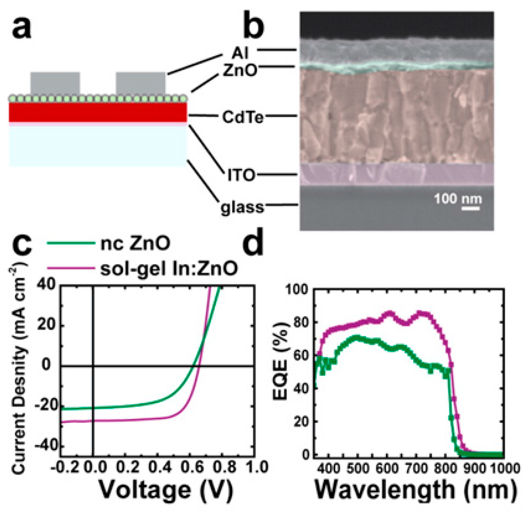
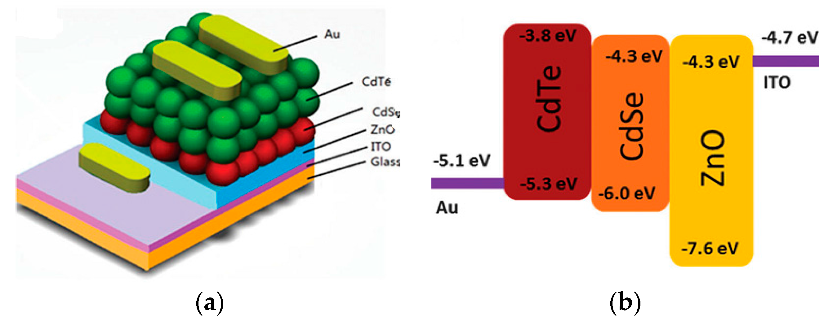
5. CdTe/ZnO Heterojunction Solar Cells

Due to the existence of defects on the interface, Fermi-level pinning generally occurs in the case of CdTe Schottky solar cells, which results in devices with low efficiency and device lifetime. CdTe solar cells with a p-n junction configuration are generally adopted in order to effectively collect photo-induced carriers. CdTe/ZnO heterojunction solar cells with CdTe as the donor and ZnO as the acceptor, is one simple p-n junction solar cell. In order to eliminate the inner stress formed by CdTe NC film with large thickness, Mulvaney et al. [8] developed a new layer-by-layer sintering approach to prepare CdTe NC thin film. As shown in Figure 4, one thin layer CdTe film was prepared by spin-casting CdTe NC solution onto the ITO substrate, then it was annealed at moderate temperature (150 ~ 350 °C) and chemical treatment, which alleviated stresses and defects formed within subsequent layers. This process was repeated several times to obtain a desired thickness (~400 nm). CdTe NC thin film prepared by this mean showed to be more compact and had few defects. ZnO film was then deposited onto the CdTe NCs film by solution processing. Ultraviolet irradiation of ZnO films was carried out for the desorption of surface-bound oxygen or carbon dioxide which, in turn, created highly-doped n-type ZnO [37,38]. They finally obtained a champion device with a PCE of 6.9% and up to 90% internal quantum efficiency. From the capacitance-voltage (C-V) curves, they concluded that the CdTe/ZnO system operated not like a p-n junction, but more like an i-n junction due to full depletion of the CdTe layer (Figure 5).
As discussed above, the contact between ITO and CdTe is not ohmic, which will decrease the device performance, especially the Voc of the device. More recently, Panthani and co-workers [39,40] adopted this layer-by-layer technique to fabricate CdTe NC solar cells with a structure of ITO/CdTe/ZnO/Al. To find out the effect of ZnO on the performance of solar cell devices, they prepared ZnO thin film by using a ZnO NC solution or a sol-gel In-doped ZnO. They obtained a certified PCE of 8.54% with In-doped ZnO thin film. It was found that In-doped ZnO devices had better device performance than those of ZnO NC devices due to the high mobility of In-doped ZnO, which improved the carrier collection efficiency (as shown in Figure 6c). To eliminate the energy barrier between ITO and CdTe, the as-prepared devices would undergo a current/light soaking process. This process resulted in a decrease in series resistance and eliminating roll-over in J-V curve. The Jsc, Voc, and FF of the best devices were 25.8 mA/cm2, 0.684 V and 0.71, respectively, resulting in a very high PCE of 12.3%, which was the highest PCE ever reported for CdTe NC solar cells. X-ray photoelectron spectroscopy (XPS) and secondary ion mass spectrometry (SIMS) were used to analyze the composition of CdTe devices and films. They found that 0.2% Cu accumulated at the sharp interfaces (Figure 7). In comparison, Cu concentrations of 5 × 1017 cm−3 were observed in the SIMS profiles of highly-efficient CdTe devices. It was really interesting that Cu tended to migrate toward the CdTe/ITO interface, which confirmed the cause of the current/light soaking effect.
Jasieniak and co-workers further studied physical, chemical, and optical properties of sintering CdTe/ZnO NCs solar cells [41]. Studies showed that the CdTe grain growth was strongly dependent on NC surface chemistry and chemical environment. Thermal annealing and CdCl2 treatment were found to be key factors to remove the organic capping ligands and grain growth of CdTe. By carefully designing the treatment of CdTe NCs thin film, solar cells with a PCE up to 7.7% and internal quantum efficiency approaching 95% were obtained. Following this, they used indium-doped ZnO as the acceptor, and a PCE above 8% was obtained. They also found that the device efficiency was up to 9.8% under forward-bias treatment/light soaking. More recently, Luther et al. [42] investigated the effects of different size, shape, and crystal structure of the initial NCs on the CdTe NC solar cells. They found that inks of predominantly wurtzite tetrapod-shaped NCs with arms about 5.6 nm in diameter formed better films than inks composed of smaller tetrapods, irregular faceted NCs, or spherical zinc blende NCs, which was consistent with the previous reports [12]. A smooth and low-defect CdTe NC film can be formed in the case of using spherical CdTe NCs because spherical NCs could assemble with higher packing density and, therefore, more easily convert into continuous films with less void space and larger grains. After optimizing the ink formulation and deposition conditions, Luther et al. found that devices annealed at 350 °C for 30 s leads to the largest grain growth and highest efficiency of 11.3% [42]. The Shockley-Queisser limit [43,44] for single and multi-junction solar cells dictates that controlling the bandgap of individual absorbing layers is vital for achieving high efficiency. To achieve high device performance, alloying is a versatile tool for engineering the optical and electronic properties of materials, which has been confirmed in CIGS- and CZT(S,Se)-based solar cells. By tuning the CdSexTe1−x film composition, Jasieniak and co-workers [9] were able to vary the optical bandgap from 1.38 eV (absorption onset 899 nm) to 1.73 eV (absorption onset 717 nm). They adopted this strategy to fabricate CdTe solar cells with a single CdTe layer, three CdSexTe1−x layers, and a ZnO NC layer. They found that the Voc was essentially independent of the alloy layer composition and the alloy based solar cells had a lower Jsc than CdTe-only devices. In such a case, the built-in voltage of the device was governed by the work function difference between the ITO and the heavily-doped ZnO layer, which was about 0.5–0.6 V. Optimizing the thickness and, therefore, the spectral absorption of the alloy layers, were very crucial to obtain high device performance.

6. CdTe/CdSe NCs Heterojunction Solar Cells

In all kinds of CdTe NC heterojunction solar cells, CdTe/CdSe NCs solar cells are the most researched system. Unlike the CdTe/ZnO system, CdTe and CdSe NCs have similar sizes and structures (zinc-blende or wurtzite), so a high-quality p-n junction is expected due to the low lattice mismatch between CdTe/CdSe NCs. In 2005, Gur et al. [6] first reported all solution-processed CdTe/CdSe NC heterojunction solar cells with structure of ITO/CdTe/CdSe/Ca/Al. By varying system parameters, the best device showed Jsc of 13.2 mA/cm2, Voc of 0.45 V, FF of 0.49, and a PCE of 2.9%. Low Voc and FF implied that the junction of CdTe/CdSe and quality of NC thin film should be further improved. Following this, many studies on the mechanism of the junction were carried out [45,46,47,48,49,50,51,52,53].
Surface photo-voltage spectroscopy was used to investigate the charge separation in Type II tunneling multilayered structures of CdTe and CdSe NCs [54]. It was found that electrons in CdSe NC layers diffuse quicker than holes in CdTe NCs layers. Carter et al. further investigated the back contact metal for electrons collected [55]. They found that Ag, Ca/Al, Au, and Al electrodes all yield similar Voc and device performance. Recently, Ju et al. [56] studied the thickness dependence on the performance of CdTe/CdSe solar cells. A low short circuit current was obtained in the case of CdTe thickness over 500 nm while very low Voc was obtained in 200 nm CdTe devices.
It is noted that all CdTe/CdSe NC solar cells discussed above have a normal structure of ITO/CdTe/CdSe/metal. Light absorption begins at the ITO, rather than the junction, many minority carriers must travel the thickness of the entire film before they are collected. Furthermore, the mismatch work function between CdTe and ITO make it difficult to obtain high Voc in this case. In 2014, Yoon et al. [57] developed a new inverted structure of ITO/CdSe/CdTe/Cr/Au, with a high Voc of 0.62 V and an efficiency of 2.1% obtained for the optimized devices. The low external quantum efficiency (EQE) obtained in the region of 400 ~ 900 nm resulted in low Jsc (below 10 mA/cm2), which was mainly caused by the large thickness (up to 100 nm) CdSe NC film used. In this case, the visible-wavelength response of the CdTe layers will be decreased. Townsend et al. [56] fabricated CdTe NCs solar cells with structure of ITO/CdSe/CdTe/Au fully by solution processing and obtained a highest PCE of 4.20%, coupled with a high Voc of 0.60 V, by carefully designing the annealing strategy. Tischler et al. [58] fabricated CdSe/CdTe NC solar cell devices treated with non-toxic salt of NH4Cl. They demonstrated minimal differences in film morphology and device performance in devices fabricated by using toxic salt of cadmium chloride or non-toxic salt of NH4Cl. More recently, Qin et al. [59] developed a novel inverted device structure of ITO/ZnO/CdSe/CdTe/Au. This devices structure has many benefits. The charge-separating interface is close to the illumination, permitting efficient collection of carriers. As shown in Figure 8, 40 nm ZnO is first deposited on ITO by decomposition of Zn precursors, following this a thin layer of CdSe NCs is deposited on ZnO. The ZnO layer provides a smooth and pinhole-free pre-layer on which a smooth CdSe film can be formed, which eliminates catastrophic shorts. In an optimized devices, Jsc of 15.28 mA/cm2, Voc of 0.65 V, and FF of 0.585 was obtained, resulting in a high PCE value of 5.81%, which was the best result ever reported for solution-processed CdTe/CdSe NC solar cells.

7. Other NC Heterojunction Solar Cells

CdS is an n-type semiconductor with a bandgap of 2.45 eV. As CdS has a similar structure as that of CdTe, the lattice mismatch is less than 5% between CdS and CdTe. CdS is the most commonly used acceptor for CdTe/CdS heterojunction solar cells. Although up to 20% PCE has been obtained in CdTe/CdS thin film solar cells prepared by chemical source deposition techniques, still few report on solution-processed CdTe NCs/CdS solar cells with satisfactory PCE. Sahoo et al. [60], for the first time, reported solution-processed CdTe NCs solar cells with a structure of ITO/CdS/CdTe/Au and negligible PCE was obtained in this case due to the poor interface between CdTe NCs and CdS. In 2013, Tian et al. [61] introduced indium-doped ZnO thin films in CdTe/CdS solar cells with a structure of ITO/ZnO-In/CdS/CdTe/MoOx/Ag, by optimizing annealing conditions, a PCE of 3.73% coupled with high-stability was obtained. More recently, Yang et al. [62] mixed CdTe and CdS NCs to form a nanoscale bulk CdTe-CdS heterojunction. They fabricated CdTe NC solar cells with a structure of ITO/TiO2/CdTe-CdS/MoO3/Au, the device showed a PCE of 3.98%, Voc of 0.50 V, Jsc of 14.81 mA/cm2, and FF of 0.538. The IQE values were about 100% in the range of 350–700 nm, implying the efficiency of charge separation. The CdTe NCs/CdS solar cells discussed above suffered from low Voc due to large defects existing on the surface of CdTe NCs and the CdS layer. In 2015, Chen et al. [63] fabricated CdTe/CdS solar cells based on CdTe and CdS NC aqueous solution. By adjusting the annealing temperature and changing the CdTe to CdS ratio, which might affect the charge dynamics and doping density, the CdTe/CdS junction quality was improved. They found that the content of S might influence the doping density of CdTe-CdS BHJ and, therefore, the depletion width of TiO2/CdTe. After optimizing the film thickness to 320 nm, they obtained the champion device with a PCE of 5.73%.
In the case of CdTe/ZnO solar cells with an inverted structure, ZnO nanorod (NR) is often used as an acceptor due to its high electron mobility, which provides direct pathways for efficient charge carrier transport [64]. However, the CdTe/ZnO devices shows low efficiency due to the poor carrier separation and collection. In order to overcome this drawback, Wang et al. [65] introduced a thin CdS interface layer into ZnO/CdTe core-shell nanorod array solar cells, a PCE of 0.72% was obtained, which was three times of the devices without a CdS interlayer. More recently, Du et al. [11] adopted a similar method to fabricate ZnO/CdS (interlayer)/CdTe solar cells with a three-dimensional structure. They found that the CdS layer could redistribute the depletion regions and eliminate interface defects. A PCE of 1.16% was obtained in optimized devices. The device’s performance may be further improved by tuning the length of the ZnO NRs.

8. Hybrid Solar Cells

Polymer/NC hybrid solar cells (HSCs) have received much attention due to the low-cost fabrication techniques, low material consumption, and potential application on flexible solar cells [66,67,68]. The presence of semiconductor NCs may provide high charge transfer rates as high-mobility inorganic semiconductor materials. Conjugated polymers, such as poly(3-hexylthiophene) (P3HT) [66], poly (1,4-phenylene vinylene) (PPV) derivatives, or poly [2-methoxy-5-(3,7-dimethyloctyl oxy)]-1,4-phenylenevinylene (MDMO-PPV), etc. [67], are often used as electron donors, while NCs, such as CdSe, CdTe, TiO2, ZnO, PbS, PbSe, etc., are used as electron collectors. The first notable HSC with a structure of ITO/P3HT:CdSe/Al was reported by Alivisatos in 2002 and a PCE of 1.7% was obtained in the this case [66]. Following this, many research groups developed new donor materials and acceptor materials, used different device structures, and optimized the phase separation of the hybrid active layer to improve the performance of HSCs.
With the development of water-soluble polymer and NC fabrication techniques, a lot of devices based on water-soluble polymer and NCs were fabricated. These solar cells devices are attractive for the environmentally-friendly processing method as using water as solvent. In 2011, Yang et al. [69] fabricated water-soluble HSCs with a structure of ITO/PEDOT:PSS/PPV:CdTe/ZnO/Al and obtained a PCE of 2.14%. They found that annealing temperature, annealing time, and active layer thickness were critical factors for the hybrid solar cells. Subsequently, this research group used an aqueous-solution-processed poly(p-phenylenevinylene) (PPV) precursor as the donor, while 2-mercaptoethylamine (MA)-stabilized CdTe NCs were used as the acceptor to fabricate an inverted planar heterojunction device and obtained a high PCE of 3.75% [70]. At the same time, they also took advantage of the materials to construct an n-i structure device. They found that before depositing the PPV:CdTe layer, the hydrophilicity of the annealed CdTe layer was improved by spin-coating an aqueous solution of CdCl2, which greatly increased the FF and Jsc of devices. A record PCE of 4.76% for HSC was achieved in this case. They found that interface modification using TiO2 as electrons transport layer and MoO3 as holes transport layer could improve the extraction of free carriers and, thus, lead to an enhancement in the Voc and FF [71]. To investigate the function of TiO2 and MoO3, they fabricated three different devices. Without the TiO2 layer, the device exhibited a low Jsc, Voc, and FF, resulting in a low PCE. The TiO2 layer provided an electron-selective contact and blocked the holes. PEDOT:PSS was also selected as hole transport layer (HTL ) to replace MoO3. However, a very pronounced S-shape in the J-V curve was obtained, which reduced the fill factor significantly. The poor performance was a result of the surface tension between PEDOT:PSS and PNV. Following this, Yang [72] and other groups [73] made a number of attempts to improve the device performance. It is worth mentioning that dip-coating gold nanoparticle (NP) films as the back electrode can be used for large-area aqueous-solution-processed HSCs [74]. Subsequently, Yang et al. [75] developed a new water-soluble poly(2,5-thienylene vinylene) (PWTV). In this case, the positive charges on the side chains of the polymer precursor could be easily eliminated after annealing under a nitrogen atmosphere. The CdTe NCs layer was employed to block the holes and increase light absorption. After annealing, effective secondary bonding was established between PWTV and CdTe, resulting in a high PCE of 4.3%. HSCs based on the aqueous-solution-processed P3HT dots and CdTe (NCs) [76] was also developed. Alloy NCs were also used as acceptors for HSCs. Cd0.75Hg0.25Te [77] colloid quantum dots (CQDs) and CdSexTe1−x NCs [78] were introduced into a water-soluble conjugated polymer to extend the spectrum response in near infrared for HSC. In order to increase the miscibility between polymers and aqueous CdTe NCs, water-soluble MEH-PPV precursor was used as a donor material for HSC. By adjusting the MEH-PPV/CdTe blending ratio and annealing temperature, the nanoscale morphology would change and a PCE of 4.20% was achieved [79]. More recently, Yang et al. [80] used a wide bandgap aqueous polymer-MPPV combined with CdTe NCs to prepare solar cell devices with an inverted structure and a champion PCE of 5.18% was obtained. The selected performance parameters of HSCs based on aqueous-processed conjugated polymer and CdTe NCs are summarized in Table 1.

9. Perspectives and Conclusions

Recent developments of CdTe NCs for photovoltaic applications have promoted synthesis methods, material and film processing techniques, and characterization and optimization of optoelectronic properties. These have enabled the solution-processed CdTe NC solar cells with AM 1.5 PCE up to 12%, which offers a new and powerful combination of power conversion efficiency and cost. CdTe NCs champion solar cell devices with all kinds of structure are summarized in Table 2.
In order to further improve the PCE and stability of CdTe NC-based solar cells, progress remains to be made on a number of key fronts. It is suggested that CdTe NCs solar cells with bulk heterojunction structure can eliminate the band edge and improve the carrier collection efficiency, which has been confirmed by our research group in the case of CdTe:CdSe NC bulk nano hetero-junction solar cells [81]. On the other hand, as the bandgap is limited, light above 900 nm cannot be used in CdTe NCs’ active layer, and multi-junction or graded bandgap devices should be designed to absorb all photons in ultraviolet (UV), visible, and infra-red regions of the solar spectrum. Recently, Dharmadasa et al. [82] developed a new graded bandgap device structure of FTO/n-ZnS/n-CdS/n-CdTe/Au. In this device structure, charge carrier annihilation is drastically reduced and photo-generated charge carriers have highest possible mobility values in nano crystalline rod-type CdS and CdTe. Their preliminary work on this graded bandgap devices showed over 10% efficiency with extremely high Jsc ~ 48 mA/cm2. In the case of organic-inorganic NCs hybrid solar cells, metal oxides have the ability to attain high efficiency as they have several scales of pores which may shorten the carrier diffusing length [83]. Using different passivation layers (ZnSe or CdS) and changing different metal oxide thicknesses are also possible ways of improving the efficiency of CdTe NC-based solar cells [84,85]. With the rapid rate of progress on CdTe NC-based solar cells, combined with further device optimization, solution-process CdTe NCs solar cells have a promising future.

Acknowledgments

This work is supported by the National Natural Science Foundation of China (Nos. 91333206, 61274062, 51073056 and 11204106), National Science Foundation for Distinguished Young Scholars of China (Grant No. 51225301).

Conflicts of Interest

The authors declare no conflicts of interest.

References

  1. Kim, G.; De García Arquer, F.P.; Yoon, Y.J.; Lan, X.; Liu, M.; Voznyy, O.; Yang, Z.; Fan, F.; Ip, A.H.; Kanjanaboos, P.; et al. High-efficiency colloidal quantum dot photovoltaics via robust self-assembled monolayers. Nano Lett. 2015, 15, 7691–7696. [Google Scholar] [CrossRef] [PubMed]
  2. Yang, Y.; Zhao, B.; Gao, Y.; Liu, H.; Tian, Y.; Qin, D.; Wu, H.; Hou, L.; Huang, W. Novel hybrid ligands for passivating PbS colloidal quantum dots to enhance the performance of solar cells. Nano-Micro Lett. 2015, 7, 325–331. [Google Scholar] [CrossRef]
  3. Chuang, C.M.; Brown, P.R.; Bulović, V.; Bawendi, M.G. Improved performance and stability in quantum dot solar cells through band alignment engineering. Nat. Mater. 2014, 13, 796–801. [Google Scholar] [CrossRef] [PubMed]
  4. Guo, Q.; Ford, G.M.; Agrawal, R.; Hillhouse, H. Ink formulation and low-temperature incorporation of sodium to yield 12% efficient Cu(In,Ga)(S,Se)2 solar cells from sulfide nanocrystal inks. Prog. Photovolt.: Res. Appl. 2013, 21, 64–71. [Google Scholar] [CrossRef]
  5. Guo, Q.; Hillhouse, H.W.; Agrawal, R. Synthesis of Cu2ZnSnS4 nanocrystal ink and its use for solar cells. J. Am. Chem. Soc. 2009, 33, 11672–11673. [Google Scholar] [CrossRef] [PubMed]
  6. Gur, I.; Fromer, N.A.; Geier, M.L.; Alivisatos, A.P. Air-stable all inorganic nanocrystal solar cells processed from solution. Science 2005, 310, 462–465. [Google Scholar] [CrossRef] [PubMed]
  7. Olson, J.D.; Rodriguez, Y.W.; Yang, L.D.; Alers, G.B.; Carter, S.A. CdTe Schottky diodes from colloidal nanocrystals. Appl. Phys. Lett. 2010, 96, 242103. [Google Scholar] [CrossRef]
  8. Jasieniak, J.; MacDonald, B.I.; Watkins, S.E.; Mulvaney, P. Solution-processed sintered nanocrystal solar cells via Layer-by-Layer assembly. Nano Lett. 2011, 11, 2856–2864. [Google Scholar] [CrossRef] [PubMed]
  9. MacDonald, B.I.; Martucci, A.; Rubanov, S.; Watkins, S.E.; Mulvaney, P.; Jasieniak, J.J. Layer-by-Layer assembly of sintered CdSexTe1–x nanocrystal solar cells. ACS Nano 2012, 6, 5995–6004. [Google Scholar] [CrossRef] [PubMed]
  10. MacDonald, B.I.; Della Gaspera, E.; Watkins, S.E.; Mulvaney, P.; Jasieniak, J.J. Enhanced photovoltaic performance of nanocrystalline CdTe/ZnO solar cells using sol-gel ZnO and positive bias treatment. J. Appl. Phys. 2014, 115, 184501. [Google Scholar] [CrossRef]
  11. Wang, J.; Ling, T.; Qiao, S.; Du, X. Double open-circuit voltage of three-dimensional ZnO/CdTe solar cells by a balancing depletion layer. ACS Appl. Mater. Interfaces 2014, 6, 14718–14723. [Google Scholar] [CrossRef] [PubMed]
  12. Sun, S.; Liu, H.; Gao, Y.; Qin, D.; Chen, J. Controlled synthesis of CdTe nanocrystals for high performanced Schottky thin film solar cells. J. Mater. Chem. 2012, 22, 19207–19212. [Google Scholar] [CrossRef]
  13. Tang, J.; Sargent, E.H. Infrared colloidal quantum dots for photovoltaics: Fundamentals and recent progress. Adv. Mater. 2011, 23, 12–29. [Google Scholar] [CrossRef] [PubMed]
  14. Shokhovets, S.; Ambacher, O.; Gobsch, G. Conduction-band dispersion relation and electron effective mass in III-V and II-VI zinc-blende semiconductors. Phys. Rev. B. 2007, 76, 125203. [Google Scholar] [CrossRef]
  15. Peng, Z.A.; Peng, X. Formation of High-Quality CdTe, CdSe, and CdS nanocrystals using CdO as precursor. J. Am. Chem. Soc. 2001, 123, 183–184. [Google Scholar] [CrossRef] [PubMed]
  16. Yu, W.W.; Qu, L.; Guo, W.; Peng, X. Experimental determination of the extinction coefficient of CdTe, CdSe, and CdS nanocrystals. Chem. Mater. 2003, 15, 2854–2860. [Google Scholar] [CrossRef]
  17. Yang, Y.A.; Wu, H.; Williams, K.R.; Cao, Y.C. Synthesis of CdSe and CdTe nanocrystals without precursor injection. Angew. Chem. 2005, 117, 6870–6873. [Google Scholar] [CrossRef]
  18. Liu, H.; Tao, H.; Yang, T.; Kong, L.; Qin, D.; Chen, J. A surfactant-free recipe for shape-controlled synthesis of CdSe nanocrystals. Nanotechnology 2011, 22, 045604. [Google Scholar] [CrossRef] [PubMed]
  19. Murray, C.B.; Noris, D.J.; Bawendi, M.G. Synthesis and characterization of nearly monodisperse CdE (E = S, Se, Te) semiconductor nanocrystallites. J. Am. Chem. Soc. 1993, 115, 8706–8715. [Google Scholar] [CrossRef]
  20. Xie, R.; Rutherford, M.; Peng, X. Formation of High-Quality I−III−VI semiconductor nanocrystals by tuning relative reactivity of cationic precursors. J. Am. Chem. Soc. 2009, 131, 5691–5697. [Google Scholar] [CrossRef] [PubMed]
  21. Han, L.; Qin, D.; Jiang, X.; Liu, Y.; Wang, L.; Chen, J.; Cao, Y. Synthesis of high quality zinc-blende CdSe nanocrystals and their application in hybrid solar cells. Nanotechnology 2006, 17, 4736–4742. [Google Scholar] [CrossRef] [PubMed]
  22. Qu, L.; Peng, Z.A.; Peng, X. Alternative routes toward high quality CdSe Nanocrystals. Nano Lett. 2001, 1, 333–337. [Google Scholar] [CrossRef]
  23. Peng, Z.A.; Peng, X. Nearly monodisperse and Shape-Controlled CdSe nanocrystals via alternative routes: Nucleation and growth. J. Am. Chem. Soc. 2002, 124, 3343–3353. [Google Scholar] [CrossRef] [PubMed]
  24. Sapra, S.; Poppe, J.; Eychmüller, A. CdSe nanorod synthesis: A new approach. Small 2007, 3, 1886–1888. [Google Scholar] [CrossRef] [PubMed]
  25. Loscutova, R.; Barron, A.R. Coating single-walled carbon nanotubes with cadmium chalcogenides. J. Mater. Chem. 2005, 15, 4346–4353. [Google Scholar] [CrossRef]
  26. Yu, W.W.; Wang, Y.A.; Peng, X. Formation and stability of size-, shape-, and Structure-Controlled CdTe nanocrystals: Ligand effects on monomers and nanocrystals. Chem. Mater. 2003, 15, 4300–4308. [Google Scholar] [CrossRef]
  27. Yu, W.W.; Peng, X. Formation of High-Quality CdS and other II−VI semiconductor Nanocrystals in noncoordinating solvents: Tunable reactivity of monomers. Angew. Chem. Int. Ed. 2002, 41, 2368–2371. [Google Scholar] [CrossRef]
  28. Li, Y.C.; Zhong, H.Z.; Li, R.; Zhou, Y.; Yang, C.H.; Li, Y.F. High-Yield fabrication and electrochemical characterization of tetrapodal CdSe, CdTe, and CdSexTe1–x nanocrystals. Adv. Funct. Mater. 2006, 16, 1705–1716. [Google Scholar] [CrossRef]
  29. Li, J.J.; Wang, Y.A.; Guo, W.; Keay, J.C.; Mishima, T.D.; Johnson, M.B.; Peng, X. Large-Scale synthesis of nearly monodisperse CdSe/CdS Core/Shell nanocrystals using Air-Stable reagents via successive ion layer adsorption and reaction. J. Am. Chem. Soc. 2003, 125, 12567–12575. [Google Scholar] [CrossRef] [PubMed]
  30. Zhang, H.; Wang, C.; Li, M.; Ji, X.; Zhang, J.; Yang, B. Fluorescent nanocrystal−polymer composites from aqueous nanocrystals: Methods without ligand exchange. Chem. Mater. 2005, 17, 4783–4788. [Google Scholar] [CrossRef]
  31. Hoppe, H.; Arnold, N.; Sariciftci, N.S.; Meissner, D. Modeling the optical absorption within conjugated polymer/fullerene-based bulk-heterojunction organic solar cells. Sol. Energy Mater. Sol. Cells 2003, 80, 105–113. [Google Scholar] [CrossRef]
  32. Yoon, W.; Foos, E.E.; Lumb, M.P. Solution processing of CdTe nanocrystals for thin-film solar cells. In Proceedings of the 2012 38th IEEE Photovoltaic Specialists Conference (PVSC), Austin, TX, USA, 3–8 June 2012; pp. 2621–2624.
  33. Gessert, T.A.; Wei, S.H.; Ma, J.; Albin, D.S.; Dhere, R.G.; Duenow, J.N.; Kuciauskas, D.; Kanevce, A.; Barnes, T.M.; Burst, J.M.; et al. Research strategies toward improving thin-film CdTe photovoltaic devices beyond 20% conversion efficiency. Sol. Energy Mater. Sol. Cells 2013, 119, 149–155. [Google Scholar] [CrossRef]
  34. Toušek, J.; Kindl, D.; Toušková, J.; Dolhov, S.; Poruba, A. Diffusion length in CdTe by measurement of photovoltage spectra in CdS/CdTe solar cells. J. Appl. Phys. 2001, 89, 460–465. [Google Scholar] [CrossRef]
  35. De Mello Donegá, C.; Liljeroth, P.; Vanmaekelbergh, D. Physicochemical evaluation of the Hot-Injection method, a synthesis route for monodisperse nanocrystals. Small 2005, 1, 1152–1162. [Google Scholar] [CrossRef] [PubMed]
  36. Zhu, J.; Yang, Y.; Gao, Y.; Qin, D.; Wu, H.; Hou, L.; Huang, W. Enhancement of open-circuit voltage and the fill factor in CdTe nanocrystal solar cells by using interface materials. Nanotechnology 2014, 25, 365203. [Google Scholar] [CrossRef] [PubMed]
  37. Lakhwani, G.; Roijmans, R.F.H.; Kronemeijer, A.J.; Gilot, J.; Janssen, R.A.J.; Meskers, S.C.J. Probing charge carrier density in a layer of photodoped ZnO nanoparticles by spectroscopic ellipsometry. J. Phys. Chem. C 2010, 114, 14804–14810. [Google Scholar] [CrossRef]
  38. Wood, A.; Giersig, M.; Hilgendorff, M.; Mulvancy, P. Size effects in ZnO: The cluster to quantum dot transition. Aust. J. Chem. 2003, 56, 1051–1057. [Google Scholar] [CrossRef]
  39. Panthani, M.G.; Kurley, J.M.; Crisp, R.W.; Dietz, T.C.; Ezzyat, T.; Luther, J.M.; Talapin, D.V. High efficiency solution processed sintered CdTe nanocrystal solar cells: The role of interfaces. Nano Lett. 2014, 14, 670–675. [Google Scholar] [CrossRef] [PubMed]
  40. Ohyama, M.; Kozuka, H.; Yoko, T. Sol-gel preparation of transparent and conductive Aluminum-Doped zinc oxide films with highly preferential crystal orientation. J. Am. Ceram. Soc. 1998, 81, 1622–1632. [Google Scholar] [CrossRef]
  41. MacDonald, B.I.; Gengenbach, T.R.; Watkins, S.E.; Mulvaney, P.; Jasieniak, J.J. Solution-processing of ultra-thin CdTe/ZnO nanocrystal solar cells. Thin Solid Films 2014, 558, 365–373. [Google Scholar] [CrossRef]
  42. Crisp, R.W.; Panthani, M.G.; Rance, W.L.; Duenow, J.N.; Parilla, P.A.; Callahan, R.; Dabney, M.S.; Berry, J.J.; Talapin, D.V.; Luther, J.M. Nanocrystal grain growth and device architectures for High-Efficiency CdTe Ink-Based photovoltaics. ACS Nano 2014, 8, 9063–9072. [Google Scholar] [CrossRef] [PubMed]
  43. Small, C.E.; Chen, S.; Subbiah, J.; Amb, C.M.; Tsang, S.W.; Reynolds, J.R.; So, F. High-efficiency inverted dithienogermole–thienopyrrolodione-based polymer solar cells. Nat. Photonics 2012, 6, 115–120. [Google Scholar] [CrossRef]
  44. Shockley, W.; Queisser, H.J. Detailed balance limit of efficiency of p-n junction solar cells. J. Appl. Phys. 1961, 32. [Google Scholar] [CrossRef]
  45. Chin, K.K. P-Doping limit and donor compensation in CdTe polycrystalline thin film solar cells. Sol. Energy Mater. Sol. Cells 2010, 94, 1627–1629. [Google Scholar] [CrossRef]
  46. Talapin, D.V.; Lee, J.; Kovalenko, M.V.; Shevchenko, E.V. Prospects of colloidal nanocrystals for electronic and optoelectronic applications. Chem. Rev. 2010, 110, 389–458. [Google Scholar] [CrossRef] [PubMed]
  47. Brown, P.R.; Lunt, R.R.; Zhao, N.; Osedach, T.P.; Wanger, D.D.; Chang, L.; Bawendi, M.G.; Bulović, V. Improved current extraction from ZnO/PbS quantum dot heterojunction photovoltaics using a MoO3 interfacial layer. Nano Lett. 2011, 11, 2955–2961. [Google Scholar] [CrossRef] [PubMed]
  48. Bezryadina, A.; France, C.; Graham, R.; Yang, L.; Carter, S.A.; Alers, G.B. Mid-gap trap states in CdTe nanoparticle solar cells. Appl. Phys. Lett. 2012, 100. [Google Scholar] [CrossRef]
  49. Kim, M.J.; Lee, J.J.; Lee, S.H.; Sohn, S.H. Study of CdTe/CdS heterostructure by CdCl2 heat treatment via in situ high temperature XRD. Sol. Energy Mater. Sol. Cell 2013, 109, 209–214. [Google Scholar] [CrossRef]
  50. Buurma, C.; Krishnamurthy, S.; Sivananthan, S. Shockley-Read-Hall lifetimes in CdTe. J. Appl. Phys. 2014, 116. [Google Scholar] [CrossRef]
  51. Chambers, B.A.; MacDonald, B.I.; Ionescu, M.; Deslandes, A.; Quinton, J.S.; Jasieniak, J.J.; Andersson, G.G. Examining the role of ultra-thin atomic layer deposited metal oxide barrier layers on CdTe/ITO interface stability during the fabrication of solution processed nanocrystalline solar cells. Sol. Energy Mater. Sol. Cell 2014, 125, 164–169. [Google Scholar] [CrossRef]
  52. Hsiao, K. Energy-band barrier to improve open-circuit voltage of CdTe solar cells. Sol. Energy Mater. Sol. Cell 2014, 120, 647–653. [Google Scholar] [CrossRef]
  53. Kosyachenko, L.; Toyama, T. Current–voltage characteristics and quantum efficiency spectra of efficient thin-film CdS/CdTe solar cells. Sol. Energy Mater. Sol. Cell 2014, 120, 512–520. [Google Scholar] [CrossRef]
  54. Gross, D.; Mora-Seró, I.; Dittrich, T.; Belaidi, A.; Mauser, C.; Houtepen, A.J.; Como, E.D.; Rogach, A.L.; Feldmann, J. Charge separation in type II tunneling multilayered structures of CdTe and CdSe nanocrystals directly proven by surface photovoltage spectroscopy. J. Am. Chem. Soc. 2010, 132, 5981–5983. [Google Scholar] [CrossRef] [PubMed]
  55. Ju, T.; Yang, L.L.; Carter, S. Thickness dependence study of inorganic CdTe/CdSe solar cells fabricated from colloidal nanoparticle solutions. J. Appl. Phys. 2010, 107, 104311. [Google Scholar] [CrossRef]
  56. Yoon, W.; Townsend, T.K.; Lumb, M.P.; Tischler, J.G.; Foos, E.E. Sintered CdTe nanocrystal thin films: Determination of optical constants and application in novel inverted heterojunction solar cells. IEEE Trans. Nanotechnol. 2014, 13, 551–556. [Google Scholar] [CrossRef]
  57. Townsend, T.K.; Foos, E.E. Fully solution processed all inorganic nanocrystal solar cells. Phys. Chem. Chem. Phys. 2014, 16, 16458–16464. [Google Scholar] [CrossRef] [PubMed]
  58. Townsend, T.K.; Heuer, W.B.; Foos, E.E.; Kowalski, E.; Yoon, W.; Tischler, J.G. Safer salts for CdTe nanocrystal solution processed solar cells: The dual roles of ligand exchange and grain growth. J. Mater. Chem. A. 2015, 3, 13057–13065. [Google Scholar] [CrossRef]
  59. Liu, H.; Tian, Y.Y.; Zhang, Y.J.; Gao, K.; Qin, D.H. Solution processed CdTe/CdSe nanocrystal solar cells with more than 5.5% efficiency by using an inverted device structure. J. Mater. Chem. C. 2015, 3, 4227–4234. [Google Scholar] [CrossRef]
  60. Katiyar, R.K.; Sahoo, S.; Gaur, A.P.S.; Singh, A.; Morell, G.; Katiyar, R.S. Studies of photovoltaic properties of nanocrystalline thin films of CdS–CdTe. J. Alloys Compd. 2011, 509, 10003–10006. [Google Scholar] [CrossRef]
  61. Tian, Y.; Zhang, Y.; Lin, Y.; Gao, K.; Zhang, Y.; Liu, K.; Yang, Q.; Zhou, X.; Qin, D.; Wu, H.; et al. Solution-processed efficient CdTe nanocrystal/CBD-CdS hetero-junction solar cells with ZnO interlayer. J. Nanoparticle Res. 2013, 15. [Google Scholar] [CrossRef]
  62. Chen, Z.; Zhang, H.; Zeng, Q.; Wang, Y.; Xu, D.; Wang, L.; Wang, H.; Yang, B. In situ construction of nanoscale CdTe-CdS bulk heterojunctions for inorganic nanocrystal solar cells. Adv. Energy Mater. 2014, 4. [Google Scholar] [CrossRef]
  63. Chen, Z.; Zeng, Q.; Liu, F.; Jin, G.; Du, X.; Du, J.; Zhang, H.; Yang, B. Efficient inorganic solar cells from aqueous nanocrystals: The impact of composition on carrier dynamics. RSC Adv. 2015, 5, 74263–74269. [Google Scholar] [CrossRef]
  64. Jean, J.; Chang, S.; Brown, P.R.; Cheng, J.J.; Rekemeyer, P.H.; Bawendi, M.G.; Gradečak, S.; Bulović, V. ZnO nanowire arrays for enhanced photocurrent in PbS quantum dot solar cells. Adv. Mater. 2013, 25, 2790–2796. [Google Scholar] [CrossRef] [PubMed]
  65. Zhang, G.; Jiang, S.; Lin, Y.; Ren, W.; Cai, H.; Wu, Y.; Zhang, Q.; Pan, N.; Luo, Y.; Wang, X. Improving the photovoltaic performance of solid-state ZnO/CdTe core–shell nanorod array solar cells using a thin CdS interfacial layer. J. Mater. Chem. A. 2014, 2, 5675–5681. [Google Scholar] [CrossRef]
  66. Huynh, W.U. Hybrid Nanorod-Polymer solar cells. Science 2002, 295, 2425–2427. [Google Scholar] [CrossRef] [PubMed]
  67. Kumar, S.; Nann, T. First solar cells based on CdTe nanoparticle/MEH-PPV composites. J. Mater. Res. 2004, 19, 1990–1994. [Google Scholar] [CrossRef]
  68. Hoppe, H.; Niggemann, M.; Winder, C.; Kraut, J.; Saricifitci, N.S. Nanoscale morphology of conjugated Polymer/Fullerene-based bulk-heterojunction solar cells. Adv. Funct. Mater. 2004, 14, 1005–1011. [Google Scholar] [CrossRef]
  69. Wei, H.; Zhang, H.; Sun, H.; Yang, B. Preparation of polymer–nanocrystals hybrid solar cells through aqueous approaches. Nano Today 2012, 7, 316–326. [Google Scholar] [CrossRef]
  70. Chen, Z.; Zhang, H.; Du, X.; Cheng, X.; Chen, X.; Jiang, Y.; Yang, B. From planar-heterojunction to n–i structure: An efficient strategy to improve short-circuit current and power conversion efficiency of aqueous-solution-processed hybrid solar cells. Energy Environ. Sci. 2013, 6, 1597–1603. [Google Scholar] [CrossRef]
  71. Chen, Z.; Zhang, H.; Yu, W.; Li, Z.; Hou, J.; Wei, H.; Yang, B. Inverted Hybrid Solar Cells from Aqueous Materials with a PCE of 3.61%. Adv. Energy Mater. 2013, 3, 433–437. [Google Scholar] [CrossRef]
  72. Wang, L.; Wang, H.; Wei, H.; Zhang, H.; Chen, Q.; Xu, H.; Han, W.; Yang, B.; Sun, H. Unraveling charge separation and transport mechanisms in Aqueous-Processed Polymer/CdTe nanocrystal hybrid solar cells. Adv. Energy Mater. 2014, 4. [Google Scholar] [CrossRef]
  73. Zhou, Y.; Eck, M.; Krüger, M. Bulk-heterojunction hybrid solar cells based on colloidal nanocrystals and conjugated polymers. Energy Environ. Sci. 2010, 3, 1851–1864. [Google Scholar] [CrossRef]
  74. Du, X.; Chen, Z.; Li, Z.; Hao, H.; Zeng, Q.; Dong, C.; Yang, B. Dip-Coated gold nanoparticle electrodes for Aqueous-Solution-Processed Large-Area solar cells. Adv. Energy Mater. 2014, 4. [Google Scholar] [CrossRef]
  75. Wei, H.; Jin, G.; Wang, L.; Hao, L.; Na, T.; Wang, Y.; Tian, W.; Sun, H.; Zhang, H.; Wang, H.; et al. Synthesis of a Water-Soluble conjugated polymer based on thiophene for an Aqueous-Processed hybrid photovoltaic and photodetector device. Adv. Mater. 2014, 26, 3655–3661. [Google Scholar] [CrossRef] [PubMed]
  76. Yao, S.; Chen, Z.; Li, F.; Xu, B.; Song, J.; Yan, L.; Jin, G.; Wen, S.; Wang, C.; Yang, B.; et al. High-Efficiency Aqueous-Solution-Processed hybrid solar cells based on P3HT dots and CdTe nanocrystals. ACS Appl. Mater. Interfaces 2015, 7, 7146–7152. [Google Scholar] [CrossRef] [PubMed]
  77. Jin, G.; Wei, H.; Na, T.; Sun, H.; Zhang, H.; Yang, B. High-Efficiency Aqueous-Processed hybrid solar cells with an enormous herschel infrared contribution. ACS Appl. Mater. Interfaces 2014, 6, 8606–8612. [Google Scholar] [CrossRef] [PubMed]
  78. Zeng, Q.; Chen, Z.; Zhao, Y.; Du, X.; Liu, F.; Jin, G.; Dong, F.; Zhang, H.; Yang, B. Aqueous-Processed inorganic thin-film solar cells based on CdSexTe1x nanocrystals: The impact of composition on photovoltaic performance. ACS Appl. Mater. Interfaces 2015, 7, 23223–23230. [Google Scholar] [CrossRef] [PubMed]
  79. Liu, F.; Chen, Z.; Du, X.; Zeng, Q.; Ji, T.; Cheng, Z.; Jin, G.; Yang, B. High efficiency aqueous-processed MEH-PPV/CdTe hybrid solar cells with a PCE of 4.20%. J. Mater. Chem. A. 2016, 4, 1105–1111. [Google Scholar] [CrossRef]
  80. Chen, Z.; Liu, F.; Zeng, Q.; Cheng, Z.; Du, X.; Jin, G.; Zhang, H.; Yang, B. Efficient aqueous-processed hybrid solar cells from a polymer with a wide bandgap. J. Mater. Chem. A. 2015, 3, 10969–10975. [Google Scholar] [CrossRef]
  81. Xie, Y.; Tan, Q.; Zhang, Z.; Lu, K.; Li, M.; Xu, W.; Qin, D.; Zhang, Y.; Hou, L.; Wu, H. Improving performance in CdTe/CdSe nanocrystals solar cells by using bulk nano-heterojunctions. J. Mater. Chem. C. 2016. [Google Scholar] [CrossRef]
  82. Dharmadasa, I.M.; Ojo, A.A.; Salim, H.I.; Dharmadasa, R. Next generation solar cells based on graded bandgap device structures utilising rod-type nano-materials. Energies 2015, 8, 5440–5458. [Google Scholar] [CrossRef]
  83. Ali, N.; Hussain, A.; Ahmed, R.; Wang, M.K.; Zhao, C.; UlHaq, B.; Fu, Y.Q. Advances in nanostructured thin film materials for solar cell applications. Renew. Sustain. Energy Rev. 2016, 59, 726–737. [Google Scholar] [CrossRef]
  84. Sehgal, P.; Narula, A.K. Quantum dot cosensitized solar cell based on PMOT@CdSe@ZnO core shell nanostructures with dual emission. J. Solid State Chem. 2016, 233, 428–437. [Google Scholar] [CrossRef]
  85. Unni, G.E.; Sasi, S.; Nair, A.S. Higher open-circuit voltage set by cobalt redox shuttle in SnO2 nanofibers-sensitized CdTe quantum dot solar cells. J. Energy Chem. 2016, 25, 481–488. [Google Scholar] [CrossRef]
Figure 1. AM 1.5 G solar spectrum from ASTM G173-03 reference spectra. The bandgaps for some common bulk semiconductors are: TiO2 3.3 eV; CdS 2.45 eV; CdSe 1.7 eV; CuInS2 1.54 eV; CdTe 1.5 eV; InP 1.34 eV; Cu2S 1.21 eV; Si 1.12 eV; CuInSe2 1.0 eV; InN 0.8 eV; Ge 0.66 eV; CuFeS2 0.6 eV; PbS 0.41 eV; InAs 0.35 eV and PbSe 0.28 eV. Reproduced with permission from [13]. Copyright 2011, John Wiley and Sons.
Applsci 06 00197 g001
Figure 2. A schematic image of the CdTe nanocrystals (NCs) solar cells: (a) the device’s structure; (b) the energy diagram; (c) the band diagram without an interlayer; and (d) the band diagram with an interlayer. Reproduced with permission from [36]. Copyright 2014, IOP Publishing.
Applsci 06 00197 g002
Figure 3. (a) J-V curve of the CdTe solar cells with a 1 nm Au interlayer (solid lines represent the simulation results, while open circles represent the experiment results); and (b) Mott-Schottky curves in dark conditions measured at a constant frequency of 1000 Hz for the CdTe NC solar cell device wihtout an Au interlayer. Reproduced with permission from [37]. Copyright 2010, IOP Publishing.
Applsci 06 00197 g003
Figure 4. A general schematic of the layer-by-layer process for developing sintered inorganic thin-film solar cells from colloidal nanocrystals. Reproduced with permission from [8]. Copyright 2011, American Chemical Society. (A) Synthesis of colloidal Nanocrystals. (B) Deposition of thin-films. (C) Chemical and thermal treatment. (D) Deposition of top metal electrode. (E) Electronic structure.
Applsci 06 00197 g004
Figure 5. (a) Schematic representations of partially- and fully-depleted abrupt heterojunctions based on the device architecture explored in this work. (b) The spatial and wavelength-dependent optical field density that has been normalized by the incoming field and the simulated exciton generation rate within the CdTe layer of an optimized device with 400 nm CdTe and 60 nm ZnO layers. The exciton generation rate is simulated with the standard AM 1.5 100 mW/cm2 irradiance as the incoming light source. Reproduced with permission from [8]. Copyright 2011, American Chemical Society.
Applsci 06 00197 g005
Figure 6. Schematic (a) and cross-sectional SEM (b) of a superstrate style device with the following structure: glass/ITO/CdTe/ZnO/Al (false color added for clarity). J-V characteristics (c) and external quantum efficiency (d) of devices prepared with colloidal nanocrystal-based ZnO (green) and sol-gel In-doped ZnO (In:ZnO; purple). Reproduced with permission from [40]. Copyright 2014, American Chemical Society.
Applsci 06 00197 g006
Figure 7. Depth profiling using (a) X-ray photoelectron spectroscopy (XPS) and (b) secondary ion mass spectrometry SIMS. The XPS data and CdCl2-treated SIMS samples (panel b, blue and black) were obtained from In:ZnO/CdTe/ITO stacks, while the untreated sample (panel b, open squares/circles) did not have a ZnO layer deposited to rule out In:ZnO film as the Cu source. The SIMS Te counts (circles) are shown as a guide to show the location of the interfaces. Reproduced with permission from [40]. Copyright 2014, American Chemical Society.
Applsci 06 00197 g007
Figure 8. (a) Schematic of the CdTe-CdSe NC solar cell devices and (b) energy diagram of the above device used in the study. Reproduced with permission from [60], Copyright 2015, Royal Society of Chemistry.
Applsci 06 00197 g008
Table 1. Selected performance parameters of HSCs (hybrid solar cells) based on aqueous-processed polymer NCs (nanocrystals).
StructureVoc (V)Jsc (mA/cm2)FF (%)PCE (%)Reference
ITO/PEDOT:PSS/PPV:CdTe/ZnO/Al0.5010.7402.14[69]
ITO/TiO2/CdTe/PPV:CdTe/MoO3/Au0.59116.0850.14.76[71]
ITO/TiO2/PNV:CdTe/MoO3/Au0.53112.553.13.61[72]
ITO/TiO2/CdTe/PPV/MoO3-sol/Au-sol0.4510.11371.71[74]
ITO/TiO2/CdTe/PWTV:CdTe/MoO3/Au0.5017.147.24.0[75]
ITO/TiO2/CdTe/P3HT:CdTe/MoO3/Au0.5416.9547.24.32[76]
ITO/TiO2/PPV:CdSexTe1−x/MoO3/Au0.55213.9443.53.35[78]
ITO/TiO2/MPPV:CdTe/MoO3/Au0.62415.1554.85.18[80]
Table 2. Selected champion CdTe NC solar cell devices.
Device StructurePCEPublished YearsReference
ITO/Au/CdTe/Al5.30%2014[37]
ITO/CdTe/ZnO/Al12.3%2014[40]
ITO/CdTe/CdSexTe1−x/ZnO/Al7.1%2012[9]
ITO/ZnO/CdSe/CdTe/Au5.81%2015[60]
ITO/TiO2/CdTe-CdS BHJ/Au5.73%2015[64]
ITO/TiO2/PPV:CdSexTe1−x/MoO3/Au3.35%2015[79]
ITO/TiO2/MPPV:CdTe/MoO3/Au5.18%2015[81]

