
Optoelectronic Devices Based on Atomically Thin Transition Metal Dichalcogenides

Abstract
:
1. Introduction
2. Basic Optical Properties
3. Photodetectors
4. Light-Emitters
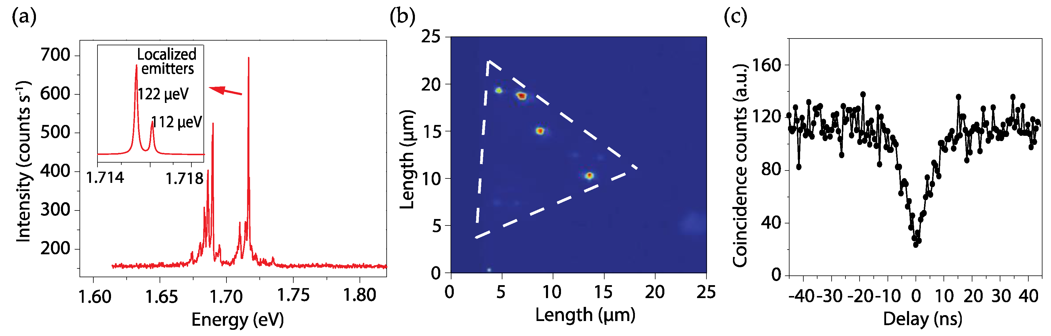
5. Single Photon Emitters
6. Photovoltaics
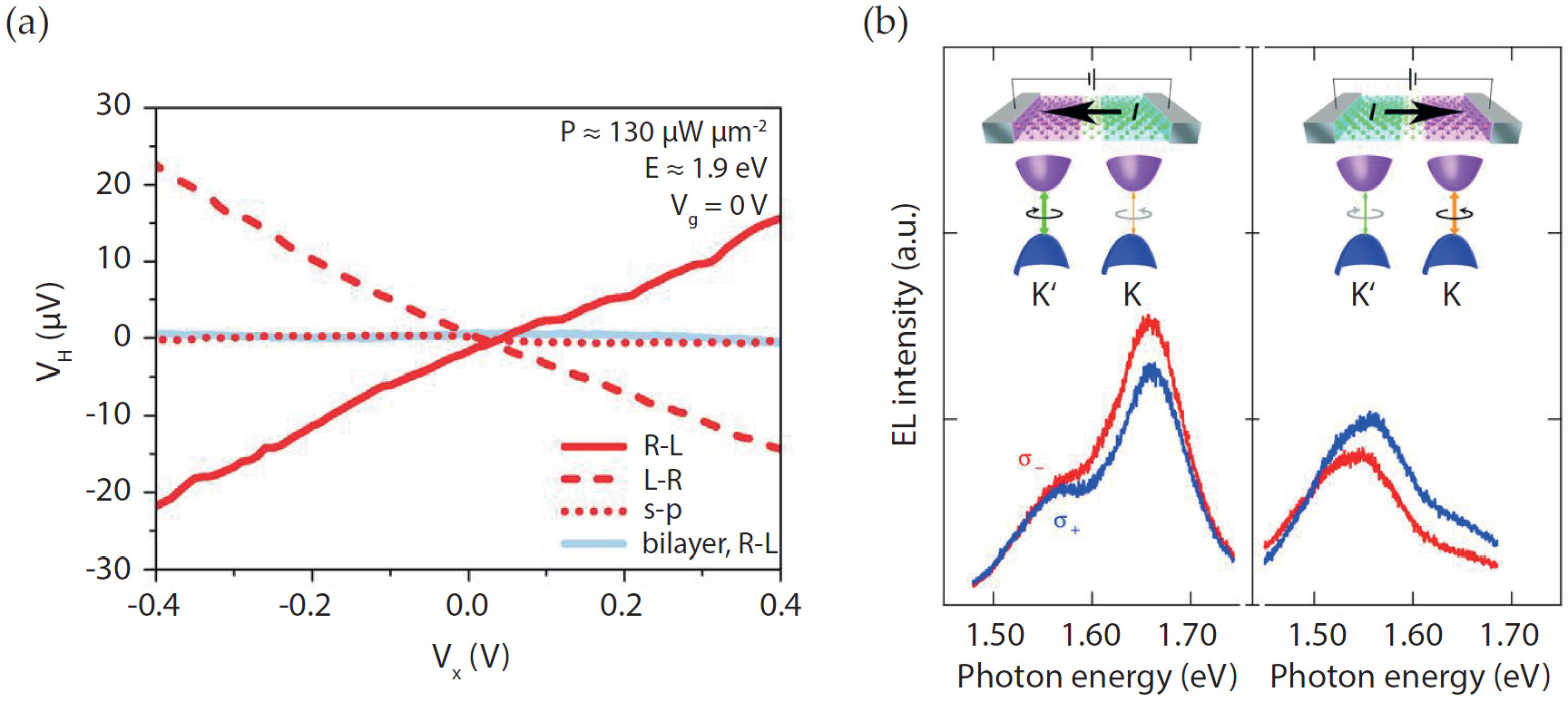
7. Valleytronics
8. Conclusions
Acknowledgments
Author Contributions
Conflicts of Interest
References
- Novoselov, K.S.; Geim, A.K.; Morozov, S.V.; Jiang, D.; Zhang, Y.; Dubonos, S.V.; Grigorieva, I.V.; Firsov, A.A. Electric field effect in atomically thin carbon films. Science 2004, 306, 666–669. [Google Scholar] [CrossRef] [PubMed]
- Novoselov, K.S.; Jiang, D.; Schedin, F.; Booth, T.J.; Khotkevich, V.V.; Morozov, S.V.; Geim, A.K. Two-dimensional atomic crystals. Proc. Natl. Acad. Sci. USA 2005, 102, 10451–10453. [Google Scholar] [CrossRef] [PubMed]
- Frindt, R.F.; Yoffe, A.D. Physical properties of layer structures: Optical properties and photoconductivity of thin crystals of molybdenum disulphide. Proc. R. Soc. A 1963, 273, 69–83. [Google Scholar] [CrossRef]
- Wilson, J.A.; Yoffe, A.D. Transition metal dichalcogenides: Discussion and interpretation of observed optical, electrical and structural properties. Adv. Phys. 1969, 18, 193–335. [Google Scholar] [CrossRef]
- Mak, K.F.; Lee, C.; Hone, J.; Shan, J.; Heinz, T.F. Atomically thin MoS2: A new direct-gap semiconductor. Phys. Rev. Lett. 2010, 105. [Google Scholar] [CrossRef] [PubMed]
- Radisavljevic, B.; Radenovic, A.; Brivio, J.; Giacometti, V.; Kis, A. Single-layer MoS2 transistors. Nat. Nanotechnol. 2011, 6, 147–150. [Google Scholar] [CrossRef] [PubMed]
- Wang, Q.H.; Kalantar-Zadeh, K.; Kis, A.; Coleman, J.N.; Strano, M.S. Electronics and optoelectronics of two-dimensional transition metal dichalcogenides. Nat. Nanotechnol. 2012, 7, 699–712. [Google Scholar] [CrossRef] [PubMed]
- Chhowalla, M.; Shin, H.S.; Eda, G.; Li, L.-J.; Loh, K.P.; Zhang, H. The chemistry of two-dimensional layered transition metal dichalcogenide nanosheets. Nat. Chem. 2013, 5, 263–275. [Google Scholar] [CrossRef] [PubMed]
- Jariwala, D.; Sangwan, V.K.; Lauhon, L.J.; Marks, T.J.; Hersam, M.C. Emerging device applications for semiconducting two-dimensional transition metal dichalcogenides. ACS Nano 2014, 8, 1102–1120. [Google Scholar] [CrossRef] [PubMed]
- Splendiani, A.; Sun, L.; Zhang, Y.; Li, T.; Kim, J.; Chim, C.-Y.; Galli, G.; Wang, F. Emerging photoluminescence in monolayer MoS2. Nano Lett. 2010, 10, 1271–1275. [Google Scholar] [CrossRef] [PubMed]
- Tonndorf, P.; Schmidt, R.; Böttger, P.; Zhang, X.; Börner, J.; Liebig, A.; Albrecht, M.; Kloc, C.; Gordan, O.; Zahn, D.R.T.; et al. Photoluminescence emission and Raman response of monolayer MoS2, MoSe2, and WSe2. Opt. Express 2013, 21, 4908–4916. [Google Scholar] [CrossRef] [PubMed]
- Amani, M.; Lien, D.-H.; Kiriya, D.; Xiao, J.; Azcatl, A.; Noh, J.; Madhvapathy, S.R.; Addou, R.; KC, S.; Dubey, M.; et al. Near-unity photoluminescence quantum yield in MoS2. Science 2015, 350, 1065–1068. [Google Scholar] [CrossRef] [PubMed]
- Han, H.V.; Lu, A.-Y.; Lu, L.-S.; Huang, J.-K.; Li, H.; Hsu, C.-L.; Lin, Y.-C.; Chiu, M.-H.; Suenaga, K.; Chu, C.-W.; et al. Photoluminescence enhancement and structure repairing of monolayer MoSe2 by hydrohalic acid treatment. ACS Nano 2016, 10, 1454–1461. [Google Scholar] [CrossRef] [PubMed]
- Klots, A.R.; Newaz, A.K.M.; Wang, B.; Prasai, D.; HKrzyzanowska, H.; Lin, J.; Caudel, D.; Ghimire, N.J.; Yan, J.; Ivanov, B.L.; et al. Probing excitonic states in suspended two-dimensional semiconductors by photocurrent spectroscopy. Sci. Rep. 2014, 4. [Google Scholar] [CrossRef] [PubMed]
- Ross, J.S.; Wu, S.; Yu, H.; Ghimire, N.J.; Jones, A.M.; Aivazian, G.; Yan, J.; Mandrus, D.G.; Xiao, D.; Yao, W.; et al. Electrical control of neutral and charged excitons in a monolayer semiconductor. Nat. Commun. 2013, 4. [Google Scholar] [CrossRef] [PubMed] [Green Version]
- Ugeda, M.M.; Bradley, A.J.; Shi, S.-F.; da Jornada, F.H.; Zhang, Y.; Qiu, D.Y.; Ruan, W.; Mo, S.-K.; Hussain, Z.; Shen, Z.-X.; et al. Giant bandgap renormalization and excitonic effects in a monolayer transition metal dichalcogenide semiconductor. Nat. Mater. 2014, 13, 1091–1095. [Google Scholar] [CrossRef] [PubMed]
- Zhao, W.; Ghorannevis, Z.; Chu, L.; Toh, M.; Kloc, C.; Tan, P.-H.; Eda, G. Evolution of electronic structure in atomically thin sheets of WS2 and WSe2. ACS Nano 2013, 7, 791–797. [Google Scholar] [CrossRef] [PubMed]
- Chernikov, A; Berkelbach, T.C.; Hill, H.M.; Rigosi, A.; Li, Y.; Aslan, O.B.; Reichman, D.R.; Hybertsen, M.S.; Heinz, T.F. Exciton binding energy and nonhydrogenic rydberg series in monolayer WS2. Phys. Rev. Lett. 2014, 113. [Google Scholar] [CrossRef]
- He, K.; Kumar, N.; Zhao, L.; Wang, Z.; Mak, K.F.; Zhao, H.; Shan, J. Tightly bound excitons in monolayer WSe2. Phys. Rev. Lett. 2014, 113. [Google Scholar] [CrossRef] [PubMed]
- Ruppert, C.; Aslan, O.B.; Heinz, T.F. Optical properties and band gap of single- and few-layer MoTe2 crystals. Nano Lett. 2014, 14, 6231–6236. [Google Scholar] [CrossRef] [PubMed]
- Kormányos, A.; Burkard, G.; Gmitra, M.; Fabian, J.; Zólyomi, V.; Drummond, N.D.; Fal’ko, V. k.p theory for two-dimensional transition metal dichalcogenide semiconductors. 2D Mater. 2015, 2. [Google Scholar] [CrossRef]
- Ramasubramaniam, A. Large excitonic effects in mono-layers of molybdenum and tungsten dichalcogenides. Phys. Rev. B 2012, 86. [Google Scholar] [CrossRef]
- Berkelbach, T.C.; Hybertsen, M.S.; Reichman, D.R. Theory of neutral and charged excitons in monolayer transition metal dichalcogenides. Phys. Rev. B 2013, 88. [Google Scholar] [CrossRef]
- Qiu, D.Y.; da Jornada, F.H.; Louie, S.G. Optical spectrum of MoS2: Many-body effects and diversity of exciton states. Phys. Rev. Lett. 2013, 111. [Google Scholar] [CrossRef] [PubMed]
- Castellanos-Gomez, A.; Roldán, R.; Cappelluti, E.; Buscema, M.; Guinea, F.; van der Zant, H.S.J.; Steele, G.A. Local strain engineering in atomically thin MoS2. Nano Lett. 2013, 13, 5361–5366. [Google Scholar] [CrossRef] [PubMed]
- Mak, K.F.; He, K.; Lee, C.; Lee, G.H.; Hone, J.; Heinz, T.F.; Shan, J.S. Tightly bound trions in monolayer MoS2. Nat. Mater. 2013, 12, 207–211. [Google Scholar] [CrossRef] [PubMed]
- Xiao, D.; Liu, G.-B.; Feng, W.; Xu, X.; Yao, W. Coupled spin and valley physics in monolayers of MoS2 and other group-VI dichalcogenides. Phys. Rev. Lett. 2012, 108. [Google Scholar] [CrossRef] [PubMed]
- Mak, K.F.; He, K.; Shan, J.; Heinz, T.F. Control of valley polarization in monolayer MoS2 by optical helicity. Nat. Nanotechnol. 2012, 7, 494–498. [Google Scholar] [CrossRef] [PubMed]
- Jones, A.M.; Yu, H.; Ghimire, N.J.; Wu, S.; Aivazian, G.; Ross, J.S.; Zhao, B.; Yan, J.; Mandrus, D.G.; Xiao, D.; et al. Optical generation of excitonic valley coherence in monolayer WSe2. Nat. Nanotechnol. 2013, 8, 634–638. [Google Scholar] [CrossRef] [PubMed]
- Koppens, F.H.L.; Mueller, T.; Avouris, Ph.; Ferrari, A.C.; Vitiello, M.S.; Polini, M. Photodetectors based on graphene, other two-dimensional materials and hybrid systems. Nat. Nanotechnol. 2014, 9, 780–793. [Google Scholar] [CrossRef] [PubMed]
- Yin, Z.; Li, H.; Li, H.; Jiang, L.; Shi, Y.; Sun, Y.; Lu, G.; Zhang, Q.; Chen, X.; Zhang, H. Single-layer MoS2 phototransistors. ACS Nano 2012, 6, 74–80. [Google Scholar] [CrossRef] [PubMed]
- Wu, C.-C.; Jariwala, D.; Sangwan, V.K.; Marks, T.J.; Hersam, M.C.; Lauhon, L.J. Elucidating the photoresponse of ultrathin MoS2 field-effect transistors by scanning photocurrent microscopy. J. Phys. Chem. Lett. 2013, 4, 2508–2513. [Google Scholar] [CrossRef]
- Buscema, M.; Barkelid, M.; Zwiller, V.; van der Zant, H.S.J.; Steele, G.A.; Castellanos-Gomez, A. Large and tunable photothermoelectric effect in single-layer MoS2. Nano Lett. 2013, 13, 358–363. [Google Scholar] [CrossRef] [PubMed]
- Pospischil, A.; Furchi, M.M.; Mueller, T. Solar-energy conversion and light emission in an atomic monolayer p-n diode. Nat. Nanotechnol. 2014, 9, 257–261. [Google Scholar] [CrossRef] [PubMed]
- Baugher, B.W.H.; Churchill, H.O.H.; Yang, Y.; Jarillo-Herrero, P. Optoelectronic devices based on electrically tunable p-n diodes in a monolayer dichalcogenide. Nat. Nanotechnol. 2014, 9, 262–267. [Google Scholar] [CrossRef] [PubMed]
- Furchi, M.M.; Pospischil, A.; Libisch, F.; Burgdörfer, J.; Mueller, T. Photovoltaic effect in an electrically tunable van der Waals heterojunction. Nano Lett. 2014, 14, 4785–4791. [Google Scholar] [CrossRef] [PubMed]
- Lee, C.-H.; Lee, G.-H.; van der Zande, A.M.; Chen, W.; Li, Y.; Han, M.; Cui, X.; Arefe, G.; Nuckolls, C.; Heinz, T.F.; et al. Atomically thin p-n junctions with van der Waals heterointerfaces. Nat. Nanotechnol. 2014, 9, 676–681. [Google Scholar] [CrossRef] [PubMed]
- Fontana, M.; Deppe, T.; Boyd, A.K.; Rinzan, M.; Liu, A.Y.; Paranjape, M.; Barbara, P. Electron-hole transport and photovoltaic effect in gated MoS2 Schottky junctions. Sci. Rep. 2013, 3. [Google Scholar] [CrossRef] [PubMed]
- Dobusch, L.; Furchi, M.M.; Pospischil, A.; Mueller, T.; Bertagnolli, E.; Lugstein, A. Electric field modulation of thermovoltage in single-layer MoS2. Appl. Phys. Lett. 2014, 105. [Google Scholar] [CrossRef]
- Lopez-Sanchez, O.; Lembke, D.; Kayci, M.; Radenovic, A.; Kis, A. Ultrasensitive photodetectors based on monolayer MoS2. Nat. Nanotechnol. 2013, 8, 497–501. [Google Scholar] [CrossRef] [PubMed]
- Furchi, M.M.; Polyushkin, D.K.; Pospischil, A.; Mueller, T. Mechanisms of photoconductivity in atomically thin MoS2. Nano Lett. 2014, 14, 6165–6170. [Google Scholar] [CrossRef] [PubMed]
- Zhang, W.; Huang, J.-K.; Chen, C.-H.; Chang, Y.-H.; Cheng, Y.-J.; Li, L.-J. High-gain phototransistors based on a CVD MoS2 monolayer. Adv. Mater. 2013, 25, 3456–3461. [Google Scholar] [CrossRef] [PubMed]
- Lee, H.S.; Min, S.-W.; Chang, Y.-G.; Park, M.K.; Nam, T.; Kim, H.; Kim, J.H.; Ryu, S.; Im, S. MoS2 nanosheet phototransistors with thickness-modulated optical energy gap. Nano Lett. 2012, 12, 3695–3700. [Google Scholar] [CrossRef] [PubMed]
- Choi, W.; Cho, M.Y.; Konar, A.; Lee, J.H.; Cha, G.-B.; Hong, S.C.; Kim, S.; Kim, J.; Jena, D.; Joo, J.; et al. High-detectivity multilayer MoS2 phototransistors with spectral response from ultraviolet to infrared. Adv. Mater. 2012, 24, 5832–5836. [Google Scholar] [CrossRef] [PubMed]
- Tsai, D.S.; Liu, K.K.; Lien, D.-H.; Tsai, M.L.; Kang, C.-F.; Lin, C.-A.; Li, L.-J.; He, J.-H. Few-layer MoS2 with high broadband photogain and fast optical switching for use in harsh environments. ACS Nano 2013, 7, 3905–3911. [Google Scholar] [CrossRef] [PubMed]
- Perea-López, N.; Perea-López, N.; Elías, A.N.; Berkdemir, A.; Castro-Beltran, A.; Gutiérrez, H.R.; Feng, S.; Lv, R.; Hayashi, T.; López-Urías, F.; et al. Photosensor device based on few-layered WS2 films. Adv. Funct. Mater. 2013, 23, 5511–5517. [Google Scholar] [CrossRef]
- Buscema, M.; Groenendijk, D.J.; Blanter, S.I.; Steele, G.A.; van der Zant, H.S.J.; Castellanos-Gomez, A. Fast and broadband photoresponse of few-layer black phosphorus field-effect transistors. Nano Lett. 2014, 14, 3347–3352. [Google Scholar] [CrossRef] [PubMed]
- Liu, F.; Shimotani, H.; Shang, H.; Kanagasekaran, T.; Zólyomi, V.; Drummond, N.; Falko, V.I.; Tanigaki, K. High-sensitivity photodetectors based on multilayer GaTe flakes. ACS Nano 2014, 8, 752–760. [Google Scholar] [CrossRef] [PubMed]
- Hu, P.; Wen, Z.; Wang, L.; Tan, P.; Xiao, K. Synthesis of few-layer GaSe nanosheets for high performance photodetectors. ACS Nano 2012, 6, 5988–5994. [Google Scholar] [CrossRef] [PubMed]
- Hu, P.; Wang, L.; Yoon, M.; Zhang, J.; Feng, W.; Wang, X.; Wen, Z.; Idrobo, J.C.; Miyamoto, Y.; Geohegan, D.B.; et al. Highly responsive ultrathin GaS nanosheet photodetectors on rigid and flexible substrates. Nano Lett. 2013, 13, 1649–1654. [Google Scholar] [CrossRef] [PubMed]
- Jacobs-Gedrim, R.B.; Shanmugam, M.; Jain, N.; Durcan, C.A.; Murphy, M.T.; Murray, T.M.; Matyi, R.J.; Moorell, R.J.; Yu, B. Extraordinary photoresponse in two-dimensional In2Se3 nanosheets. ACS Nano 2014, 8, 514–521. [Google Scholar] [CrossRef] [PubMed]
- Abderrahmane, A.; Ko, P.J.; Thu, T.V.; Ishizawa, S.; Takamura, T.; Sandhu, A. High photosensitivity few-layered MoSe2 back-gated field-effect phototransistors. Nanotechnol. 2014, 25. [Google Scholar] [CrossRef] [PubMed]
- Kang, H.-S.; Choi, C.-S.; Choi, W.-Y.; Kim, D.-H.; Seo, K.-S. Characterization of phototransistor internal gain in metamorphic high-electron-mobility transistors. Appl. Phys. Lett. 2004, 84. [Google Scholar] [CrossRef]
- Kufer, D.; Konstantatos, G. Highly sensitive, encapsulated MoS2 Photodetector with gate controllable gain and speed. Nano Lett. 2015, 15, 7307–7313. [Google Scholar]
- Konstantatos, G.; Badioli, M.; Gaudreau, L.; Osmond, J.; Bernechea, M.; de Arquer, F.P.G.; Gatti, F.; Koppens, F.H.L. Hybrid graphene-quantum dot phototransistors with ultrahigh gain. Nat. Nanotechnol. 2012, 7, 363–368. [Google Scholar] [CrossRef] [PubMed]
- Roy, K.; Padmanabhan, M.; Goswami, S.; Sai, T.P.; Ramalingam, G.; Raghavan, S.; Ghosh, A. Graphene-MoS2 hybrid structures for multifunctional photoresponsive memory devices. Nat. Nanotechnol. 2013, 8, 826–830. [Google Scholar] [CrossRef] [PubMed]
- Kufer, D.; Nikitskiy, I.; Lasanta, T.; Navickaite, G.; Koppens, F.H.L.; Konstantatos, G. Hybrid 2D–0D MoS2-PbS quantum dot photodetectors. Adv. Mater. 2015, 27, 176–180. [Google Scholar] [CrossRef] [PubMed]
- Geim, A.K.; Grigorieva, I.V. Van der Waals heterostructures. Nature 2013, 499, 419–425. [Google Scholar] [CrossRef] [PubMed]
- Yu, W.J.; Liu, Y.; Zhou, H.; Yin, A.; Li, Z.; Huang, Y.; Duan, X. Highly efficient gate-tunable photocurrent generation in vertical heterostructures of layered materials. Nat. Nanotechnol. 2013, 8, 952–958. [Google Scholar] [CrossRef] [PubMed]
- Britnell, L.; Ribeiro, R.M.; Eckmann, A.; Jalil, R.; Belle, B.D.; Mishchenko, A.; Kim, Y.-J.; Gorbachev, R.V.; Georgiou, T.; Morozov, S.V.; et al. Strong light-matter interactions in heterostructures of atomically thin films. Science 2013, 340, 1311–1314. [Google Scholar] [CrossRef] [PubMed]
- Yang, W.; Yang, H.; Qin, G.; Ma, Z.; Berggren, J.; Hammar, M.; Soref, R.; Zhou, W. Large-area InP-based crystalline nanomembrane flexible photodetectors. Appl. Phys. Lett. 2010, 96. [Google Scholar] [CrossRef]
- Kautek, W. Electronic mobility anisotropy of layered semiconductors: Transversal photoconductivity measurements at n-MoSe2. J. Phys. C Solid State Phys. 1982, 15. [Google Scholar] [CrossRef]
- Massicotte, M.; Schmidt, P.; Vialla, F.; Schädler, K.G.; Reserbat-Plantey, A.; Watanabe, K.; Taniguchi, T.; Tielrooij, K.J.; Koppens, F.H.L. Picosecond photoresponse in van der Waals heterostructures. Nat. Nanotechnol. 2016, 11, 42–46. [Google Scholar] [CrossRef] [PubMed]
- Li, D.; Cheng, R.; Zhou, H.; Wang, C.; Yin, A.; Chen, Y.; Weiss, N.O.; Huang, Y.; Duan, X. Electric-field-induced strong enhancement of electroluminescence in multilayer molybdenum disulfide. Nat. Commun. 2015, 6. [Google Scholar] [CrossRef] [PubMed]
- Zhang, Y.J.; Oka, T.; Suzuki, R.; Ye, J.T.; Iwasa, Y. Electrically switchable chiral light-emitting transistor. Science 2014, 344, 725–728. [Google Scholar] [CrossRef] [PubMed]
- Li, Z.; Ezhilarasu, G.; Chatzakis, I.; Dhall, R.; Chen, C.-C.; Cronin, S.B. Indirect band gap emission by hot electron injection in metal/MoS2 and metal/WSe2 heterojunctions. Nano Lett. 2015, 15, 3977–3982. [Google Scholar] [CrossRef] [PubMed]
- Sundaram, R.S.; Engel, M.; Lombardo, A.; Krupke, R.; Ferrari, A.C.; Avouris, P.; Steiner, M. Electroluminescence in single layer MoS2. Nano Lett. 2013, 13, 1416–1421. [Google Scholar] [CrossRef] [PubMed]
- Chen, J.; Perebeinos, V.; Freitag, M.; Tsang, J.; Fu, Q.; Liu, J.; Avouris, P. Bright infrared emission from electrically induced excitons in carbon nanotubes. Science 2005, 310, 1171–1174. [Google Scholar] [CrossRef] [PubMed]
- Doh, Y.-J.; Maher, K.N.; Ouyang, L.; Yu, C.L.; Park, H.; Park, J. Electrically driven light emission from individual CdSe nanowires. Nano Lett. 2008, 8, 4552–4556. [Google Scholar] [CrossRef] [PubMed]
- Ponomarev, E.; Gutierrez-Lezama, I.; Ubrig, N.; Morpurgo, A.F. Ambipolar light-emitting transistors on chemical vapor deposited monolayer MoS2. Nano Lett. 2015, 15, 8289–8294. [Google Scholar] [CrossRef] [PubMed]
- Choi, M.S.; Qu, D.; Lee, D.; Liu, X.; Watanabe, K.; Taniguchi, T.; Yoo, W.J. Lateral MoS2 p-n junction formed by chemical doping for use in high-performance optoelectronics. ACS Nano 2014, 8, 9332–9340. [Google Scholar] [CrossRef] [PubMed]
- Ross, J.S.; Klement, P.; Jones, A.M.; Ghimire, N.J.; Yan, J.; Mandrus, D.G.; Taniguchi, T.; Watanabe, K.; Kitamura, K.; Yao, W.; et al. Electrically tunable excitonic light-emitting diodes based on monolayer WSe2 p-n junctions. Nat. Nanotechnol. 2014, 9, 268–272. [Google Scholar] [CrossRef] [PubMed]
- Jo, S.; Ubrig, N.; Berger, H.; Kuzmenko, A.B.; Morpurgo, A.F. Mono- and bilayer WS2 light-emitting transistors. Nano Lett. 2014, 14, 2019–2025. [Google Scholar] [CrossRef] [PubMed]
- Lopez-Sanchez, O.; Llado, E.A.; Koman, V.; Fontcuberta i Morral, A.; Radenovic, A.; Kis, A. Light generation and harvesting in a van der Waals heterostructure. ACS Nano 2014, 8, 3042–3048. [Google Scholar] [CrossRef] [PubMed]
- Withers, F.; del Pozo-Zamudio, O.; Mishchenko, A.; Rooney, A.P.; Gholinia, A.; Watanabe, K.; Taniguchi, T.; Haigh, S.J.; Geim, A.K.; Tartakovskii, A.I.; et al. Light-emitting diodes by band-structure engineering in van der Waals heterostructures. Nat. Mater. 2015, 14, 301–306. [Google Scholar] [CrossRef] [PubMed]
- Ye, Y.; Ye, Z.; Gharghi, M.; Zhu, H.; Zhao, M.; Yin, X.; Zhang, X. Exciton-related electroluminescence from monolayer MoS2. Appl. Phys. Lett. 2014, 104. [Google Scholar] [CrossRef]
- Withers, F.; del Pozo-Zamudio, O.; Schwarz, S.; Dufferwiel, S.; Walker, P.M.; Godde, T.; Rooney, A.P.; Gholinia, A.; Woods, C.R.; Blake, P.; et al. WSe2 light-emitting tunneling transistors with enhanced brightness at room temperature. Nano Lett. 2015, 15, 8223–8228. [Google Scholar] [CrossRef] [PubMed]
- Schwarz, S.; Dufferwiel, S.; Walker, P.M.; Withers, F.; Trichet, A.A.P.; Sich, M.; Li, F.; Chekhovich, E.A.; Borisenko, D.N.; Kolesnikov, N.N.; et al. Two-dimensional metal-chalcogenide films in tunable optical microcavities. Nano Lett. 2014, 14, 7003–7008. [Google Scholar] [CrossRef] [PubMed]
- Wu, S.; Buckley, S.; Jones, A.M.; Ross, J.S.; Ghimire, N.J.; Yan, J.; Mandrus, D.G.; Yao, W.; Hatami, F.; Vučković, J.; et al. Control of two-dimensional excitonic light emission via photonic crystal. 2D Mater. 2014, 1. [Google Scholar] [CrossRef]
- Reed, J.C.; Zhu, A.Y.; Zhu, H.; Yi, F.; Cubukcu, E. Wavelength tunable microdisk cavity light source with a chemically enhanced MoS2 emitter. Nano Lett. 2015, 15, 1967–1971. [Google Scholar] [CrossRef] [PubMed]
- Wu, S.; Buckley, S.; Schaibley, J.R.; Feng, L.; Yan, J.; Mandrus, D.G.; Hatami, F.; Yao, W.; Vučković, J.; Majumdar, A.; et al. Monolayer semiconductor nanocavity lasers with ultralow thresholds. Nature 2015, 520, 69–72. [Google Scholar] [CrossRef] [PubMed] [Green Version]
- Salehzadeh, O.; Djavid, M.; Tran, N.H.; Shih, I.; Mi, Z. Optically pumped two-dimensional MoS2 lasers operating at room-temperature. Nano Lett. 2015, 15, 5302–5306. [Google Scholar] [CrossRef] [PubMed]
- Ye, Y.; Wong, Z.J.; Lu, X.; Ni, X.; Zhu, H.; Chen, X.; Wang, Y.; Zhang, X. Monolayer excitonic laser. Nat. Photonics 2015, 9, 733–737. [Google Scholar] [CrossRef]
- Tonndorf, P.; Schmidt, R.; Schneider, R.; Kern, J.; Buscema, M.; Steele, G.A.; Castellanos-Gomez, A.; van der Zant, H.S.J.; de Vasconcellos, S.M.; Bratschitsch, R. Single-photon emission from localized excitons in an atomically thin semiconductor. Optica 2015, 2, 347–352. [Google Scholar] [CrossRef]
- Srivastava, A.; Sidler, M.; Allain, A.V.; Lembke, D.S.; Kis, A.; Imamoglu, A. Optically active quantum dots in monolayer WSe2. Nat. Nanotechnol. 2015, 10, 491–496. [Google Scholar] [CrossRef] [PubMed]
- He, Y.-M.; Clark, G.; Schaibley, J.R.; He, Y.; Chen, M.-C.; Wei, Y.-J.; Ding, X.; Zhang, Q.; Yao, W.; Xu, X.; et al. Single quantum emitters in monolayer semiconductors. Nat. Nanotechnol. 2015, 10, 497–502. [Google Scholar] [CrossRef] [PubMed]
- Koperski, M.; Nogajewski, K.; Arora, A.; Cherkez, V.; Mallet, P.; Veuillen, J.Y.; Marcus, J.; Kossacki, P.; Potemski, M. Single photon emitters in exfoliated WSe2 structures. Nat. Nanotechnol. 2015, 10, 503–506. [Google Scholar] [CrossRef] [PubMed]
- Chakraborty, C.; Kinnischtzke, L.; Goodfellow, K.M.; Beams, R.; Vamivakas, A.N. Voltage-controlled quantum light from an atomically thin semiconductor. Nat. Nanotechnol. 2015, 10, 507–511. [Google Scholar] [CrossRef] [PubMed]
- Palummo, M.; Bernardi, M.; Grossman, J.C. Exciton radiative lifetimes in two-dimensional transition metal dichalcogenides. Nano Lett. 2015, 15, 2794–2800. [Google Scholar] [CrossRef] [PubMed]
- Tran, T.T.; Bray, K.; Ford, M.J.; Toth, M.; Aharonovich, I. Quantum emission from hexagonal boron nitride monolayers. Nat. Nanotechnol. 2015, 11, 37–41. [Google Scholar] [CrossRef] [PubMed]
- Li, Y.; Chernikov, A.; Zhang, X.; Rigosi, A.; Hill, H.M.; van der Zande, A.M.; Chenet, D.A.; Shih, E.-M.; Hone, J.; Heinz, T.F. Measurement of the optical dielectric function of monolayer transition-metal dichalcogenides: MoS2, MoSe2, WS2 and WSe2. Phys. Rev. B 2014, 90. [Google Scholar] [CrossRef]
- Bernardi, M.; Palummo, M.; Grossman, J.C. Extraordinary sunlight absorption and one nanometer thick photovoltaics using two-dimensional monolayer materials. Nano Lett. 2013, 13, 3664–3670. [Google Scholar] [CrossRef] [PubMed]
- Gan, L.-Y.; Zhang, Q.; Cheng, Y.; Schwingenschlögl, U. Photovoltaic heterojunctions of fullerenes with MoS2 and WS2 monolayers. J. Phys. Chem. Lett. 2014, 5, 1445–1449. [Google Scholar] [CrossRef] [PubMed]
- Echtermeyer, T.J.; Britnell, L.; Jasnos, P.K.; Lombardo, A.; Gorbachev, R.V.; Grigorenko, A.N.; Geim, A.K.; Ferrari, A.C.; Novoselov, K.S. Strong plasmonic enhancement of photovoltage in graphene. Nat. Commun. 2011, 2. [Google Scholar] [CrossRef] [PubMed]
- Clemen, C.; Saldana, X.I.; Munz, P.; Bucher, E. Photovoltaic properties of some semiconducting layer structures. Phys. Status Solidi A 1978, 49, 437–443. [Google Scholar] [CrossRef]
- Memaran, S.; Pradhan, N.R.; Lu, Z.; Rhodes, D.; Ludwig, J.; Zhou, Q.; Ogunsolu, O.; Ajayan, P.M.; Smirnov, D.; Fernandez-Dominguez, A.I.; et al. Pronounced photovoltaic response from multilayered transition-metal Dichalcogenides PN-Junctions. Nano Lett. 2015, 15, 7532–7538. [Google Scholar] [CrossRef] [PubMed]
- Groenendijk, D.J.; Buscema, M.; Steele, G.A.; de Vasconcellos, S.M.; Bratschitsch, R.; van der Zant, H.S.J.; Castellanos-Gomez, A. Photovoltaic and photothermoelectric effect in a double-gated WSe2 device. Nano Lett. 2014, 14, 5846–5852. [Google Scholar] [CrossRef] [PubMed]
- Buscema, M.; Groenendijk, D.J.; Steele, G.A.; van der Zant, H.S.J.; Castellanos-Gomez, A. Photovoltaic effect in few-layer black phosphorus PN junctions defined by local electrostatic gating. Nat. Commun. 2014, 5. [Google Scholar] [CrossRef] [PubMed]
- Flöry, N.; Jain, A.; Bharadwaj, P.; Parzefall, M.; Taniguchi, T.; Watanabe, K.; Novotny, L. A WSe2/MoSe2 heterostructure photovoltaic device. Appl. Phys. Lett. 2015, 107. [Google Scholar] [CrossRef]
- Cheng, R.; Li, D.; Zhou, H.; Wang, C.; Yin, A.; Jiang, S.; Liu, Y.; Chen, Y.; Huang, Y.; Duan, X. Electroluminescence and photocurrent generation from atomically sharp WSe2/MoS2 heterojunction p-n Diodes. Nano Lett. 2014, 14, 5590–5597. [Google Scholar] [CrossRef] [PubMed]
- Hong, X.; Kim, J.; Shi, S.F.; Zhang, Y.; Jin, C.; Sun, Y.; Tongay, S.; Wu, J.; Zhang, Y.; Wang, F. Ultrafast charge transfer in atomically thin MoS2/WS2 heterostructures. Nat. Nanotechnol. 2014, 9, 682–686. [Google Scholar] [CrossRef] [PubMed]
- Rivera, P.; Schaibley, J.R.; Jones, A.M.; Ross, J.S.; Wu, S.; Aivazian, G.; Klement, P.; Seyler, K.L.; Clark, G.; Ghimire, N.J.; et al. Observation of long-lived interlayer excitons in monolayer MoSe2–WSe2 heterostructures. Nat. Commun. 2015, 6. [Google Scholar] [CrossRef] [PubMed] [Green Version]
- Yu, Y.; Hu, S.; Su, L.; Huang, L.; Liu, Y.; Jin, Z.; Purezky, A.A.; Geohegan, D.B.; Kim, K.W.; Zhang, Y.; et al. Equally efficient interlayer exciton relaxation and improved absorption in epitaxial and nonepitaxial MoS2/WS2 heterostructures. Nano Lett. 2015, 15, 486–491. [Google Scholar] [CrossRef] [PubMed]
- Wang, F.; Wang, Z.; Xu, K.; Wang, F.; Wang, Q.; Huang, Y.; Yin, L.; He, J. Tunable GaTe-MoS2 van der Waals p-n Junctions with novel optoelectronic performance. Nano Lett. 2015, 15, 7558–7566. [Google Scholar] [CrossRef] [PubMed]
- Cheng, H.-C.; Wang, G.; Li, D.; He, Q.; Yin, A.; Liu, Y.; Wu, H.; Ding, M.; Huang, Y.; Duan, X. van der Waals heterojunction devices based on organohalide perovskites and two-dimensional materials. Nano Lett. 2016, 16, 367–373. [Google Scholar] [CrossRef] [PubMed]
- Wi, S.; Chen, M.; Li, D.; Nam, H.; Meyhofer, E.; Liang, X. Photovoltaic response in pristine WSe2 layers modulated by metal-induced surface-charge-transfer doping. Appl. Phys. Lett. 2015, 107. [Google Scholar] [CrossRef]
- Velez, S.; Ciudad, D.; Island, J.; Buscema, M.; Txoperena, O.; Parui, S.; Steele, G.A.; Casanova, F.; van der Zant, H.S.J.; Castellanos-Gomez, A.; et al. Gate-tunable diode and photovoltaic effect in an organic-2D layered material p-n junction. Nanoscale 2015, 7, 15442–15449. [Google Scholar] [CrossRef] [PubMed]
- He, D.; Pan, Y.; Nan, H.; Gu, S.; Yang, Z.; Wu, B.; Luo, X.; Xu, B.; Zhang, Y.; Li, Y.; et al. A van der Waals p-n heterojunction with organic/inorganic semiconductors. Appl. Phys. Lett. 2015, 107. [Google Scholar] [CrossRef]
- Jariwala, D.; Howell, S.L.; Chen, K.-S.; Kang, J.; Sangwan, V.K.; Filippone, S.A.; Turrisi, R.; Marks, T.J.; Lauhon, L.J.; Hersam, M.C. Hybrid, gate-tunable, van der Waals p-n heterojunctions from pentacene and MoS2. Nano Lett. 2015, 16, 497–503. [Google Scholar] [CrossRef] [PubMed]
- Xu, X.; Yao, W.; Xiao, D.; Heinz, T.F. Spin and pseudospins in layered transition metal dichalcogenides. Nat. Phys. 2014, 10, 343–350. [Google Scholar] [CrossRef]
- Zeng, H.; Dai, J.; Yao, W.; Xiao, D.; Cui, X. Valley polarization in MoS2 monolayers by optical pumping. Nat. Nanotechnol. 2012, 7, 490–493. [Google Scholar] [CrossRef] [PubMed]
- Cao, T.; Wang, G.; Han, W.; Ye, H.; Zhu, C.; Shi, J.; Niu, Q.; Tan, P.; Wang, E.; Liu, B.; et al. Valley-selective circular dichroism of monolayer molybdenum disulphide. Nat. Commun. 2012, 3. [Google Scholar] [CrossRef] [PubMed]
- Srivastava, A.; Sidler, M.; Allain, A.V.; Lembke, D.S.; Kis, A.; Imamoglu, A. Valley Zeeman effect in elementary optical excitations of monolayer WSe2. Nat. Phys. 2015, 11, 141–147. [Google Scholar] [CrossRef]
- Mak, K.F.; McGill, K.L.; Park, J.; McEuen, P.L. The valley Hall effect in MoS2 transistors. Science 2014, 344, 1489–1492. [Google Scholar] [CrossRef] [PubMed]
- Eginligil, M.; Cao, B.; Wang, Z.; Shen, X.; Cong, C.; Shang, J.; Soci, C.; Yu, T. Dichroic spin-valley photocurrent in monolayer molybdenum disulphide. Nat. Commun. 2015, 6. [Google Scholar] [CrossRef] [PubMed]
- Yuan, H.; Wang, X.; Lian, B.; Zhang, H.; Fang, X.; Shen, B.; Xu, G.; Xu, Y.; Zhang, S.-C.; Hwang, H.Y.; et al. Generation and electric control of spin–valley-coupled circular photogalvanic current in WSe2. Nat. Nanotechnol. 2014, 9, 851–857. [Google Scholar] [CrossRef] [PubMed]
- Zhan, Y.; Liu, Z.; Najmaei, S.; Ajayan, P.M.; Lou, J. Large-area vapor-phase growth and characterization of MoS2 atomic layers on a SiO2 substrate. Small 2012, 8, 966–971. [Google Scholar] [CrossRef] [PubMed]
- Yu, Y.; Li, C.; Liu, Y.; Su, L.; Zhang, Y.; Cao, L. Controlled scalable synthesis of uniform, high-quality monolayer and few-layer MoS2 films. Sci. Rep. 2013, 3. [Google Scholar] [CrossRef] [PubMed]
- Dumcenco, D.; Ovchinnikov, D.; Marinov, K.; Lazić, P.; Gibertini, M.; Marzari, N.; Sanchez, O.L.; Kung, Y.-C.; Krasnozhon, D.; Chen, M.-W.; et al. Large-area epitaxial monolayer MoS2. ACS Nano 2015, 9, 4611–4620. [Google Scholar] [CrossRef] [PubMed]
- Huang, J.-K.; Pu, J.; Hsu, C.-L.; Chiu, M.-H.; Juang, Z.-Y.; Chang, Y.-H.; Chang, W.-H.; Iwasa, Y.; Takenobu, T.; Li, L.-J. Large-area synthesis of highly crystalline WSe2 monolayers and device applications. ACS Nano 2014, 8, 923–930. [Google Scholar] [CrossRef] [PubMed]
- Wang, X.; Gong, Y.; Shi, G.; Chow, W.L.; Keyshar, K.; Ye, G.; Vajtai, R.; Lou, J.; Liu, Z.; Ringe, E.; et al. Chemical vapor deposition growth of crystalline monolayer MoSe2. ACS Nano 2014, 8, 5125–5131. [Google Scholar] [CrossRef] [PubMed]
- Huang, C.; Wu, S.; Sanchez, A.M.; Peters, J.J.P.; Beanland, R.; Ross, J.S.; Rivera, P.; Yao, W.; Cobden, D.H.; Xu, X. Lateral heterojunctions within monolayer MoSe2–WSe2 semiconductors. Nat. Mater. 2014, 13, 1096–1101. [Google Scholar] [CrossRef] [PubMed]
- Li, J.; Östling, M. Scalable Fabrication of 2D Semiconducting crystals for future electronics. Electronics 2015, 4, 1033–1061. [Google Scholar] [CrossRef]
- Kang, K.; Xie, S.; Huang, L.; Han, Y.; Huang, P.Y.; Mak, K.F.; Kim, C.-J.; Muller, D.; Park, J. High-mobility three-atom-thick semiconducting films with wafer-scale homogeneity. Nature 2015, 520, 656–660. [Google Scholar] [CrossRef] [PubMed]
- Li, M.-Y.; Shi, Y.; Cheng, C.-C.; Lu, L.-S.; Lin, Y.-C.; Tang, H.-L.; Tsai, M.-L.; Chu, C.-W.; Wei, K.-H.; He, J.-H.; et al. Epitaxial growth of a monolayer WSe2-MoS2 lateral p-n junction with an atomically sharp interface. Science 2015, 349, 524–528. [Google Scholar] [CrossRef] [PubMed]
- Lin, Z.; Zhao, Y.; Zhou, C.; Zhong, R.; Wang, X.; Tsang, Y.H.; Chai, Y. Controllable growth of large-size crystalline MoS2 and resist-free transfer assisted with a Cu thin film. Sci. Rep. 2015, 5. [Google Scholar] [CrossRef] [PubMed]
- Gong, Y.; Lin, J.; Wang, X.; Shi, G.; Lei, S.; Lin, Z.; Zou, X.; Ye, G.; Vajtai, R.; Yakobson, B.I.; et al. Vertical and in-plane heterostructures from WS2/MoS2 monolayers. Nat. Mater. 2014, 13, 1135–1142. [Google Scholar] [CrossRef] [PubMed]


© 2016 by the authors; licensee MDPI, Basel, Switzerland. This article is an open access article distributed under the terms and conditions of the Creative Commons by Attribution (CC-BY) license (http://creativecommons.org/licenses/by/4.0/).
Share and Cite
Pospischil, A.; Mueller, T. Optoelectronic Devices Based on Atomically Thin Transition Metal Dichalcogenides. Appl. Sci. 2016, 6, 78. https://doi.org/10.3390/app6030078
Pospischil A, Mueller T. Optoelectronic Devices Based on Atomically Thin Transition Metal Dichalcogenides. Applied Sciences. 2016; 6(3):78. https://doi.org/10.3390/app6030078
Chicago/Turabian StylePospischil, Andreas, and Thomas Mueller. 2016. "Optoelectronic Devices Based on Atomically Thin Transition Metal Dichalcogenides" Applied Sciences 6, no. 3: 78. https://doi.org/10.3390/app6030078