Article

Digital Controller Design Based on Active Damping Method of Capacitor Current Feedback for Auxiliary Resonant Snubber Inverter with LC Filter

Department of Electrical Engineering, Harbin Institute of Technology, Harbin 150080, China
*
Author to whom correspondence should be addressed.
Appl. Sci. 2016, 6(11), 377; https://doi.org/10.3390/app6110377
Submission received: 3 October 2016 / Revised: 15 November 2016 / Accepted: 16 November 2016 / Published: 22 November 2016

Abstract

:
In some high-performance applications, an LC filter must be added to the auxiliary resonant snubber inverter (ARSI) to reduce the output current ripple. However, resonance occurs due to the additional LC filter, which makes the traditional closed-loop control not suitable to be used directly. Therefore, this paper presents a double-loop digital control based on the active damping method of capacitor current feedback to stabilize the system. Most of the studies on active damping methods are focused on the grid in consideration of zero resistance. However, the load resistance should not be neglected in the drive system. Therefore, the load resistance and digital control delays are considered in this paper. Moreover, an improved loading method is proposed to improve the duty ratio range. In order to verify the effectiveness of the controller, a prototype was developed. The simulation and experimental results demonstrate that soft-switching can be realized for the entire load range. The maximum duty ratio is improved by 0.01 by using the proposed loading method. The resonance can be eliminated by using the proposed control method.

1. Introduction

In power electronic converters, high switching frequency is a highly desirable feature, which can not only reduce the volume and power density of converters, but also increase the dynamic response. However, high switching frequency brings about the problems of high switching loss and severe electromagnetic interference (EMI) [1,2]. The soft switching technique is one of the best options to address the problems above. To date, a variety of soft-switching DC-AC topologies have been proposed. Among them, the zero-voltage-transition (ZVT) pulse-width-modulation (PWM) inverter is a typical soft-switching inverter [3,4,5,6,7,8,9,10,11]. An auxiliary circuit connected parallel to the main power path is employed in the ZVT PWM inverter, which only operates for a short interval before and after the commutation period of the main switches. This makes the ZVT inverter closest to the PWM converter counterpart. Compared with other soft-switching inverters, the voltage and current stresses and conduction losses are much lower [3,4]. Contributing to these advantages, the ZVT PWM inverter is well accepted.
Several topologies of the ZVT PWM inverter have been proposed. The auxiliary resonant commutated pole inverter (ARCPI) has been proposed with two auxiliary switches per phase [5,6]. The ARCPI can meet the demand for high efficiency and low voltage and current stresses. However, the major drawback is the existence of the split capacitors, which cause the problems of capacitor charge unbalance. The auxiliary resonant snubber inverter (ARSI) has been proposed to eliminate the split capacitors, but the three-phase topology cannot utilize the conventional space-vector-pulse-width modulation (SVPWM) [7,8]. Thus, they are more suitable for permanent magnet brushless DC motors instead of all types of motors. The single-phase topology is very attractive with only two auxiliary switches and well fit to the conventional PWM. Meanwhile, the ZVT inverter using coupled magnetics has been proposed to eliminate the split capacitors [9,10,11]. However, these topologies need coupled inductors and a large number of auxiliary switches, which increases the cost and difficulty of the circuit realization. The ZVT PWM converter has been synthesized and summarized in [3,4].
In high-precision motor drive applications, an LC filter must be added in the ARSI to reduce the output current ripple. Moreover, the additional LC filter can solve problems of poor insulation that result from the overvoltage [12]. However, since the additional LC filter together with the inductor of the motor forms the LCL filter, a resonance peak occurs in the system, which makes the system unstable. Recently, the passive damping method has been used to stabilize the system [13,14]. The passive components of resistors, capacitors, and inductors are parallel or series-connected to the filter capacitor to damp out the resonance. The method is easy to implement; however, it reduces the efficiency of the system. The active damping method can be used to damp out the resonance at no expense of efficiency. The state variable feedback, such as filter capacitor voltage [15,16] or filter capacitor current [17,18], is introduced to provide virtual resistance. Among them, the capacitor current feedback is a typical and widely used method.
Most studies of the active damping method have focused on the grid with consideration of zero resistance. However, in the drive system, the load resistance should not be neglected. Until now, only a few researchers have studied the active damping in the motor drive system; however, they have not taken into consideration the digital control delays. In addition, previous studies on ARSI have focused on the circuit design and auxiliary current control but there has been a lack of research about the design of the closed-loop control. Thus, a step-by-step closed-loop controller design of the ARSI with LC filter is proposed in this paper, including the auxiliary current controller and the output current controller. A double-loop control based on active damping method of capacitor current feedback and PI regulator is introduced. The load resistance and digital control delays are considered. Moreover, an improved loading scheme of digital PWM (DPWM) is proposed to improve the duty ratio range of the ARSI. Finally, simulations and experiments are carried out to verify the effectiveness of the proposed method.

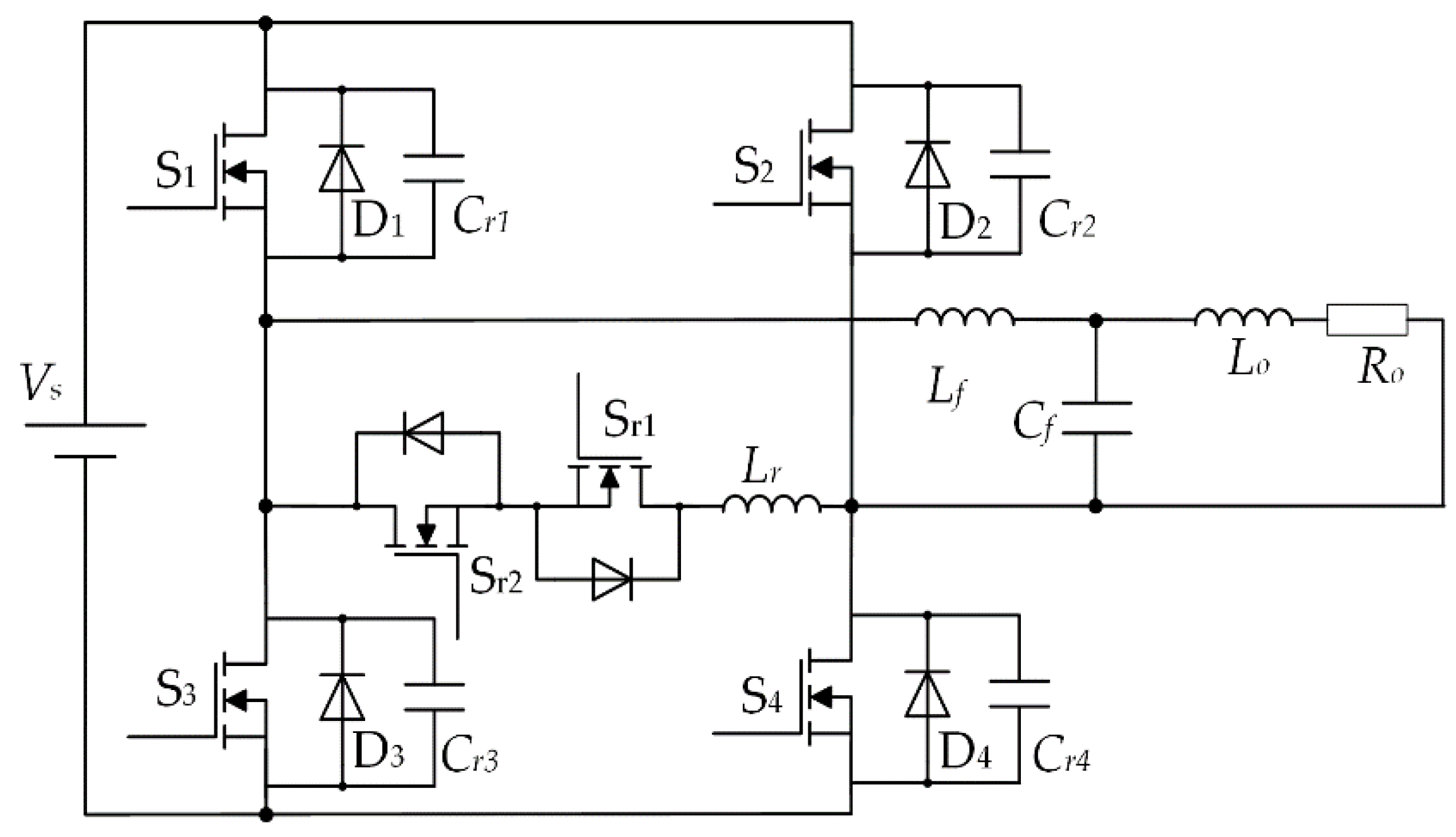
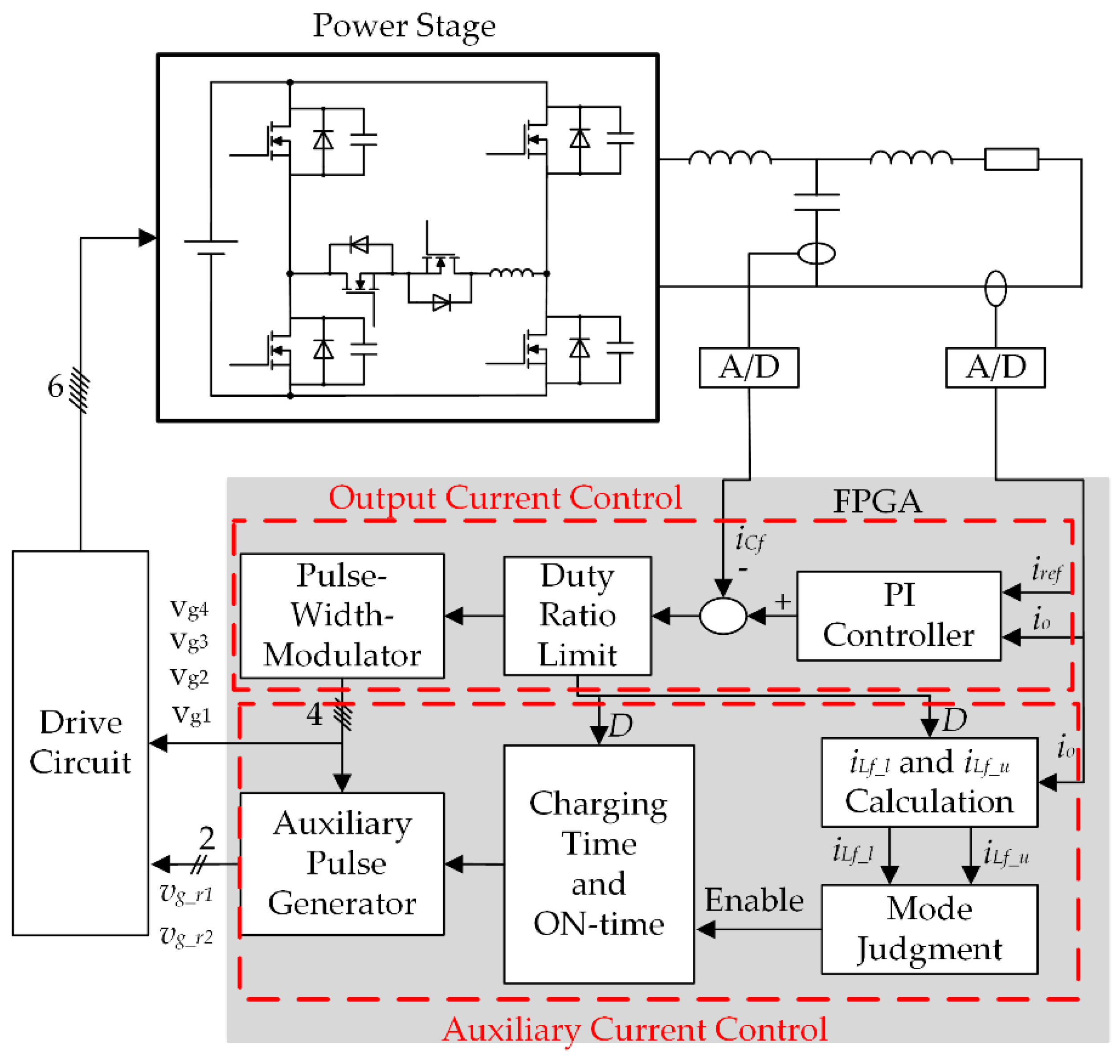
2. Control of the ARSI

Figure 1 depicts the single-phase ARSI topology analyzed in this paper, which consists of a standard H-bridge inverter, an auxiliary circuit, and an LC filter. The proper operation of the auxiliary switches Sr1 and Sr2 can create zero-voltage-switching (ZVS) conditions for the main switches S1–S4. Meanwhile, the auxiliary switches can realize zero-current switching (ZCS).
Figure 2 shows a control diagram of the ARSI. The ARSI controller consists of an output current controller and an auxiliary current controller. In the output current controller, the driving signals of the main switches are generated according to the output current. In order to dampen the resonance caused by the LC filter, a filter capacitor current feedback is introduced. The auxiliary current controller aims to control the auxiliary current to achieve ZVS of the main switches. Due to the large amount of calculations and the need for logic sequential control in the auxiliary current controller, a digital controller is required.
The auxiliary current control involves two methods, fixed-timing control [19] and variable-timing control [20]. Owing to the advantages of lower conduction losses and achieving soft-switching for a wide load range, variable-time control methods are more widely used. By using the variable-timing control, the auxiliary current follows the magnitude of the load current adaptively. The auxiliary current controller in Figure 2 is realized based on the variable-timing control. The auxiliary controller is influenced by the output current controller, whereas the output current controller is independent of the auxiliary current controller.

3. The Load Adaptive Auxiliary Current Control
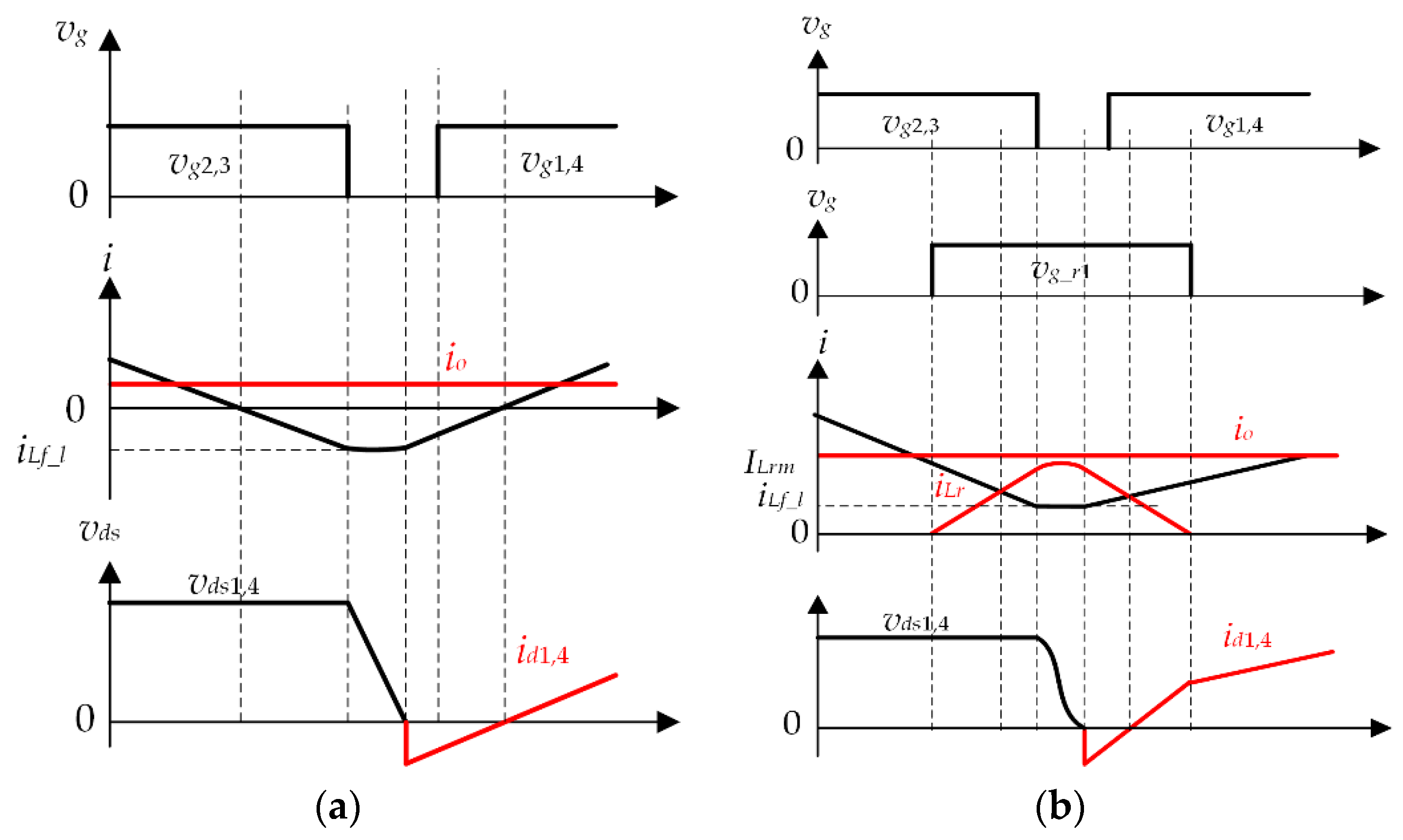
3.1. Principle

Essentially, the ZVS realization of the main switches is to obtain a proper initial resonant current Ir, in order to discharge the resonant capacitors to zero voltage before the main switches are turned on. Figure 3 shows the key waveforms to realize ZVS of S1 and S4, where vds is the drain-source voltage of a MOSFET, id is the drain current of a MOSFET, vg is the gate signal, iLf is the filter inductor current, iLf_l is the lower envelope of iLf, iLf_u is the upper envelope of iLf, and iLr is the auxiliary current. When iLf_l < −Ir_min, iLf_l can create natural ZVS (NZVS) conditions for S1 and S4 without the operation of auxiliary switches. When iLf_l > −Ir_min, Sr1 is turned on before S2 and S3 are turned off. The resonant inductor Lr is charged, resulting in the linear increase of the auxiliary current. Therefore, a proper Ir can be obtained with the operation of Sr1. The auxiliary ZVS (AZVS) of S1 and S4 is realized. In order to fully discharge the resonant capacitors, the minimum initial resonant current must meet the following requirement:
I r _ min 2 C r V s t d e a d .
The principle of ARSI without LC filter was introduced in [21]. The initial resonant current is the difference between the auxiliary current and the output current. Namely, the required auxiliary current is the sum of the output current and initial resonant current. As for the ARSI with LC filter, the auxiliary current is the sum of the filter inductor envelope current and the initial resonant current, which is different from that of the ARSI without LC filter.
The filter current ripple can be calculated as follows:
Δ i L f = V s v o L f D T s = ( 2 2 D ) D V s T s L f ,
where vo is the output voltage, D is the duty ratio, and Ts is the switching period.
The upper and lower envelopes of the filter inductor current can be calculated as follows:
i L f _ u = i o + 1 2 Δ i L f = i o + ( 1 D ) D V s T s L f
i L f _ l = i o 1 2 Δ i L f = i o ( 1 D ) D V s T s L f .
The ZVS realization of S1 and S4 is related to the lower envelope of the filter inductor current iLf_l shown in Figure 3. Similarly, the ZVS realization of S2 and S3 is related to the upper envelope of the filter inductor current iLf_u. Table 1 shows the ZVS types under different load conditions.
The output current can be obtained through the current sensor. Therefore, the required auxiliary current can be calculated as follows:
I L r m = { I r + i L f _ l f o r S r 1 I r i L f _ u f o r S r 2 .
The charging rate and the discharging rate of the resonant inductor are the same because of the same voltage Vs. Therefore, the charging time of the resonant inductor tch and the on-time of the auxiliary switch tA can be calculated as follows:
t c h = L r I L r m V s
t A = 2 t c h + t d e a d .
After generating the driving signals of the main switches, the gate signal of the auxiliary switches can be generated from Equations (6) and (7).

3.2. Limitation of the Duty Ratio

In the ARSI, to guarantee the ZVS of one set of switches, the auxiliary circuit must be turned on before the opposite set of switches is turned off. Subsequently, the resonant inductor can be charged to the required current. Therefore, the minimum on-time of the opposite set of switches must be longer than the maximum charging time of the resonant inductor. This requirement limits the maximum duty ratio Dmax.
Figure 4 shows the DPWM diagram of the ARSI. The triangle carrier is adopted due to its lower harmonic compared to the sawtooth carrier [22]. Moreover, the current is synchronously sampled at twice the PWM carrier interval, which can eliminate the switching current ripple from the current samples without needing low-pass filtering or complex ripple elimination filters [23]. Then the calculated reference voltage vc is loaded into a modulator at the point of upper limit and lower limit of the reference voltage Vupperlimit and Vlowerlimit, instead of the conventional loading point Vcmax and Vcmin. The proposed loading method can improve the maximum duty ratio. The reason is given as follows:
In order to achieve ZVS from zero load to full load, the minimum on-time of the main switches must be longer than the maximum charging time of the resonant inductor:
t o n _ min t c h _ max .
The maximum charging time occurs when the output current reaches its maximum value Io_max. The minimum on-time of the main switches occurs when the duty ratio reaches Dmax. Figure 5 shows the DPWM diagram at the condition of Io_max and Dmax. Figure 5a shows the conventional loading scheme, namely loading at Vcmax and Vcmin. The Kth current is sampled at the point Vcmin. Then the data are loaded at the next Vcmax after calculation. Subsequently, Sr1 can be turned on to charge the resonant inductor. Therefore, the following requirement must be met based on Equation (8):
T s 2 ( V c max V c min ) ( V c max V u p p e r l i m i t ) t c h _ max .
The upper limit of the reference voltage can be obtained from Equation (9):
V u p p e r l i m i t V c max 2 ( V c max V c min ) t c h _ max T s .
The maximum duty ratio Dmax occurs when ton_min equals tch_max. However, Figure 5a shows that ton_min is still longer than tch_max in this case. Only after the Kth data are loaded at Vcmax, Sr1 can be controlled. In this case, a short time cannot be utilized.
In order to improve Dmax, an improved loading scheme is adopted in which the data are loaded at Vupperlimit and Vlowerlimit. In this case, Sr1 can be turned on in advance. Furthermore, this loading scheme will not influence the gate signal generation of the main switches because the reference voltage vc is limited between Vupperlimit and Vlowerlimit. Figure 5b shows that ton_min equals tch_max by using the improved loading scheme, which improves Dmax.
In the improved loading scheme, the following requirement must be satisfied based on Equation (8):
T s 2 ( V c max V c min ) · 2 ( V c max V u p p e r lim i t ) t d e a d t c h _ max .
The upper limit of the reference voltage can be obtained from Equation (11):
V u p p e r l i m i t V c max ( V c max V c min ) ( t c h _ max + t d e a d ) T s .
From Equations (10) and (12), the limit of the reference voltage vc can be improved by adopting the improved loading scheme, resulting in larger Dmax.

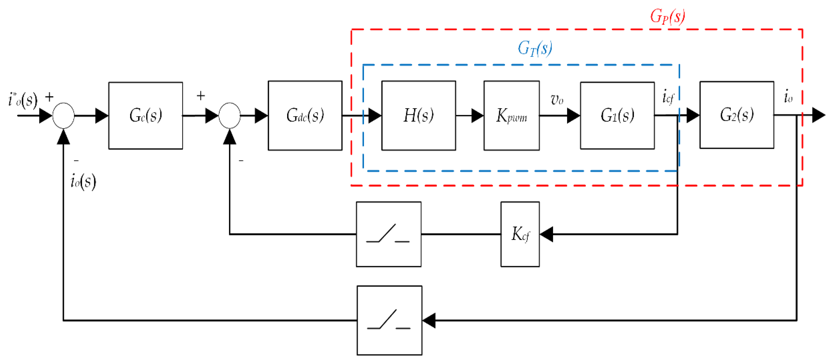
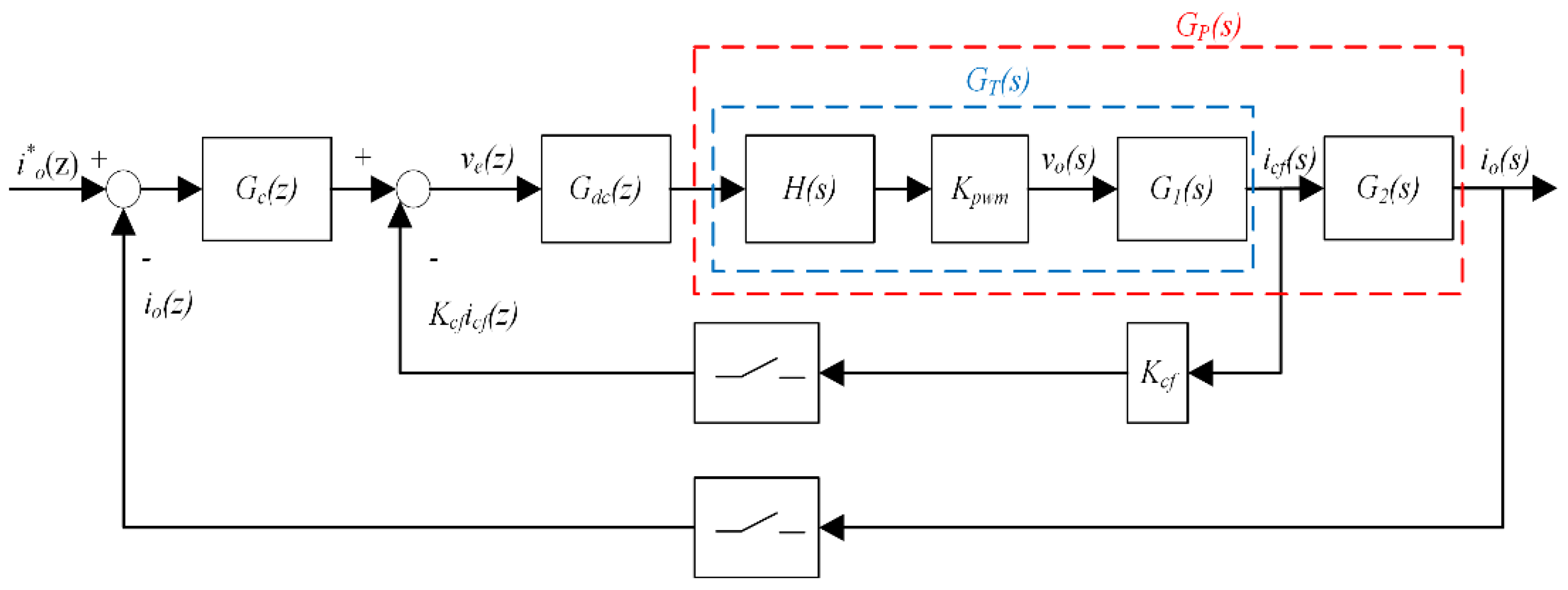
4. Output Current Control

4.1. The Model of the ARSI

Figure 6 shows the digital control model of the output current controller, where Gc(z) is the proportional integral (PI) regulator, Gdc(z) is the calculation and transport delay, the sampling switch stands for analog digital converter, Kpwm is the gain of the ARSI, Kcf is the filter capacitor current feedback coefficient, and G1(s) and G2(s) are the output impedance. In the digital controller, all the calculations and operations are discrete. Therefore, the digital controller is modeled on the z-domain.

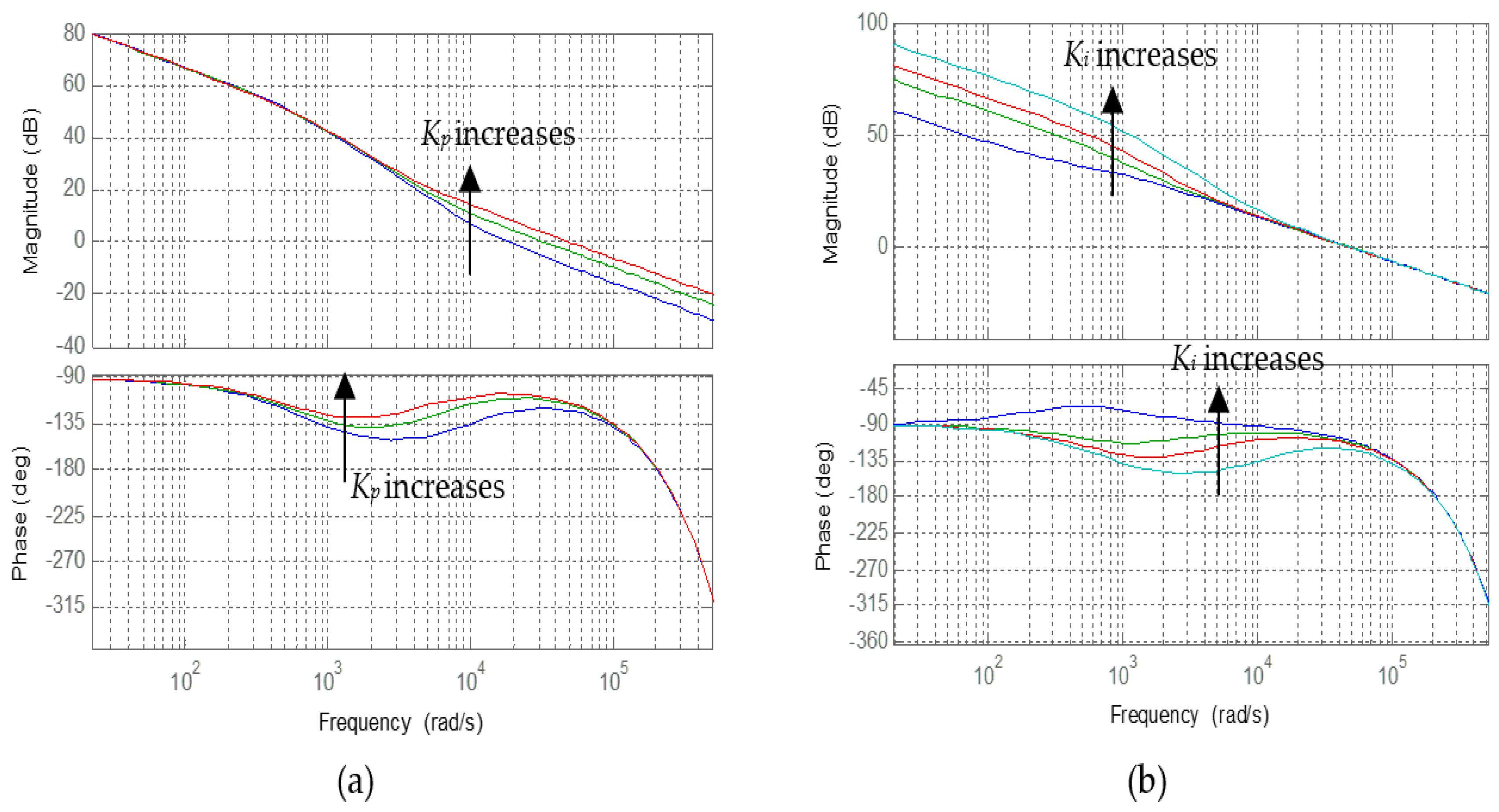
4.2. PI Controller Design

Commonly, the sample period is short and the time constant of the controlled plant is much larger than the sample period. Therefore, the digital PI controller can be designed in the s-domain. Figure 7 shows the output current controller model in the s-domain.
The PI regulator Gc(s) can be written as follows:
G c ( s ) = K p + K i s .
After the current is sampled, a sampling period delay Tsp exists, which is shown in Figure 4. Therefore, the calculation and transport delay can be written as follows:
G d c ( s ) = e T s p s ,
where the sampling period Tsp = Ts/2.
In the s-domain, the sampling switch can be modeled as 1/Tsp [24]. The modulator can be modeled by zero-order holder (ZOH) [25], which can be expressed as:
H ( s ) = 1 e T s p s s T s p e 0.5 T s p s .
Commonly, the cutoff frequency of the LC filter is larger than the bandwidth frequency of the ARSI. Therefore, the filter inductance is much lower than the load inductance, namely Lf << Lo. The output impedance can be written as follows:
G 1 ( s ) = i c f ( s ) v o ( s ) = s 2 L o C f + s R o C f s 3 L f C f L o + s 2 L f C f R o + s ( L o + L f ) + R o s C f s 2 L f C f + 1
G 2 ( s ) = i o ( s ) i c f ( s ) = 1 s 2 L o C f + s R o C f .
The system open-loop transfer function can be calculated as follows:
G ( s ) = i o ( s ) i o * ( s ) i o ( s ) = ( K p + K i s ) · K p w m e 1.5 T s p s ( s 2 L f C f + 1 ) ( s L o + R o ) + s K p w m K c f e 1.5 T s p s C f ( s L o + R o ) .
The closed-loop transfer function can be written as follows:
T ( s ) = i o ( s ) i o * ( s ) = G d c ( s ) G c ( s ) G P ( s ) 1 + K c f G d c ( s ) G T ( s ) + G d c ( s ) G c ( s ) G P ( s ) .
In order not to reduce the bandwidth of the ARSI, the cutoff frequency of the LC filter is designed to be two times larger than the system bandwidth fc. Therefore, the influence of the filter capacitor can be ignored when calculating the magnitude of the loop gain at fc and frequencies lower than fc. The low-frequency controller characteristics will still be dominated by the series filter inductance. Thus, the transfer Equation (18) can be approximated as follows:
G ( s ) ( K p + K i s ) · K p w m e 1.5 T s p s s L o + R o .
Figure 8 shows the Bode plots of the approximation model (20) and the precise model (18). It demonstrates that the cutoff frequency of the system will not be influenced by using the approximation model.
When the crossover frequency and phase margin are specified as ωc and φm respectively, the parameters of the PI controller can be obtained:
{ K p = ( L o ω c ) 2 + R o 2 K p w m 1 + 1 tan 2 ( π 2 + 1.5 ω c T s p + ϕ m + arctan ω c L o R o ) K i = ω c K p tan ( π 2 + 1.5 ω c T s p + ϕ m + arctan ω c L o R o ) .
If Kp >> Ki/ωc, Equation (21) can be approximated as:
{ K p = ( L o ω c ) 2 + R o 2 K p w m K i = ω c K p tan ( π 2 + 1.5 ω c T s p + ϕ m + arctan ω c L o R o ) .
Figure 9 shows the Bode plot of the ARSI with different PI parameters. The circuit parameters are listed in Table 2. When Kp >> Ki/ωc, the crossover frequency ωc is determined by Kp. The larger Kp, the larger ωc and the faster the dynamic response. Regarding Ki, it will influence the low-frequency gain, which can influence the stable precision of the system. The larger Ki, the larger the low-frequency gain and the higher the stable precision. Ki has almost no influence on the frequency characteristic around ωc when Kp >> Ki/ωc. However, when Ki/ωc is close to Kp, Ki will influence the phase margin. The larger Ki, the smaller the phase margin.

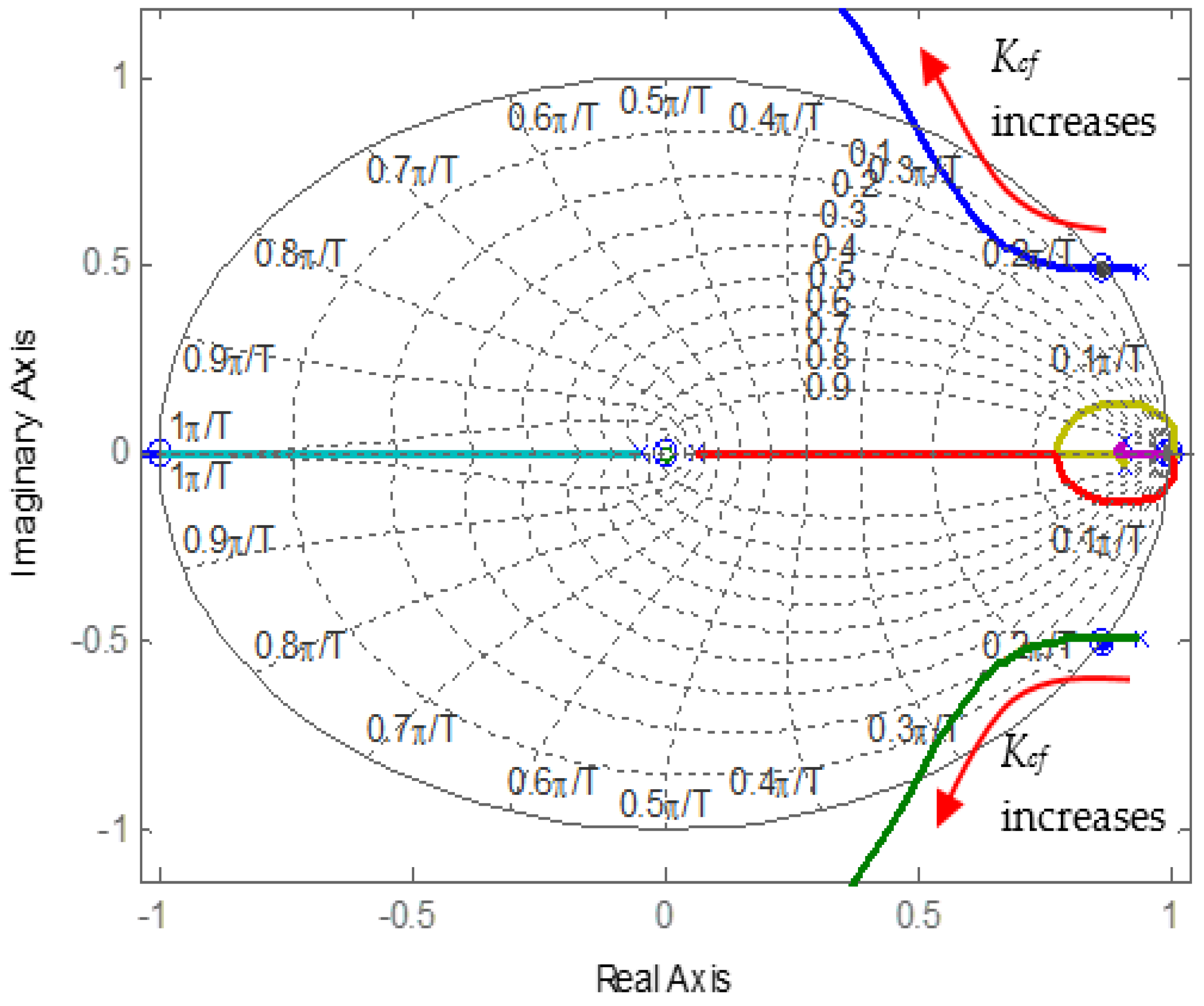
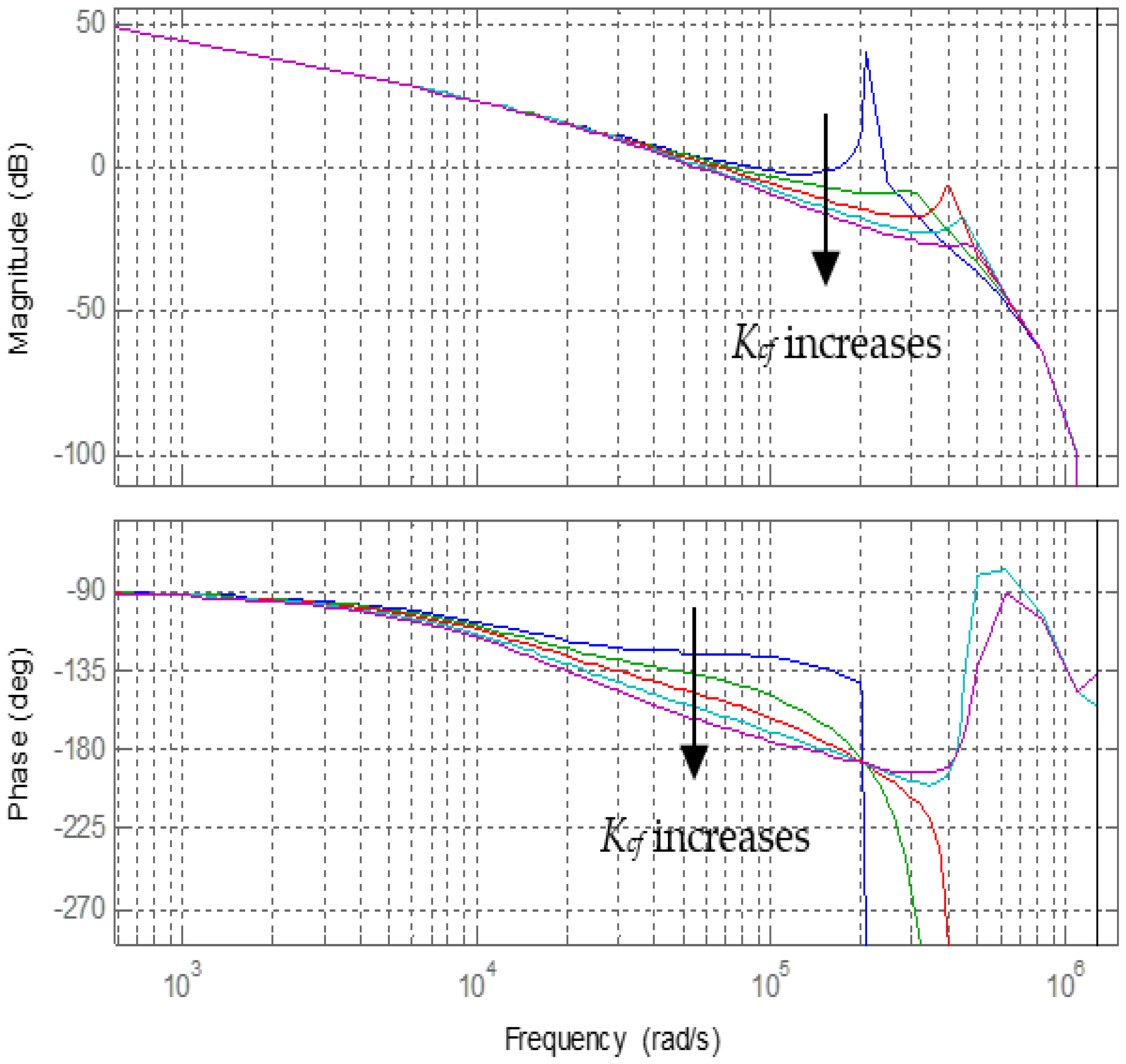
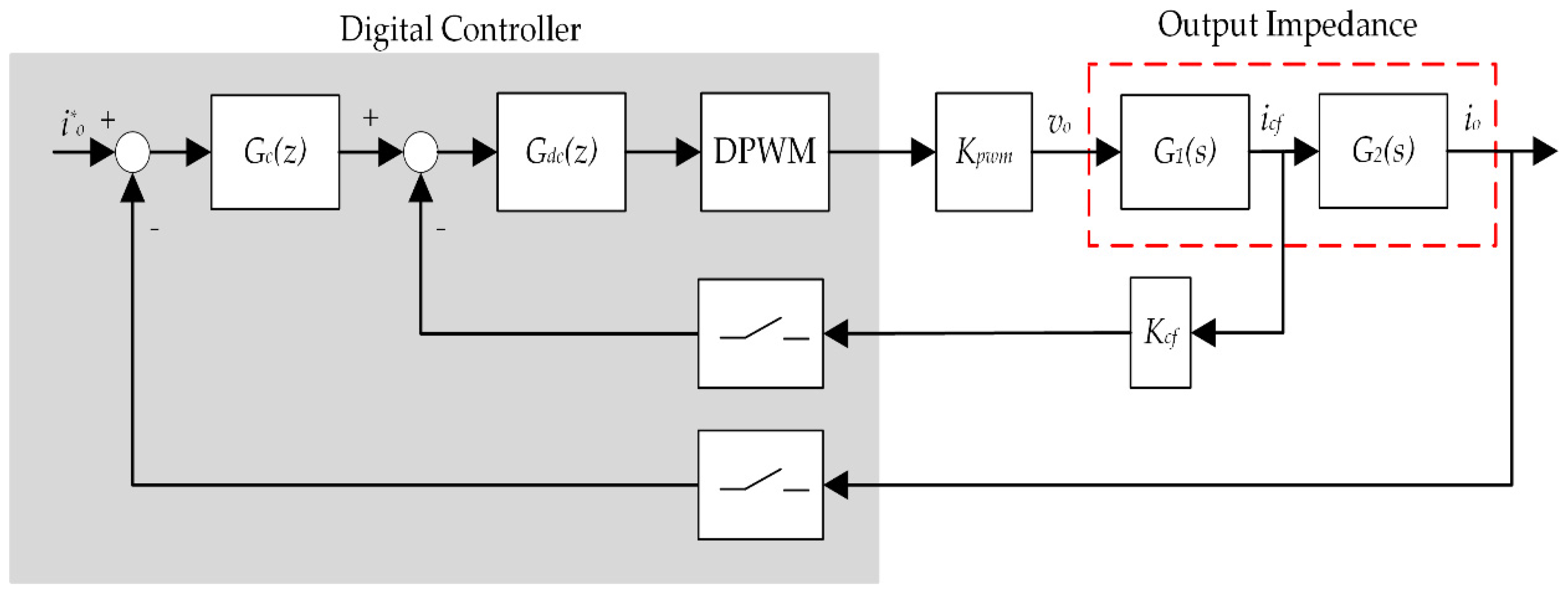
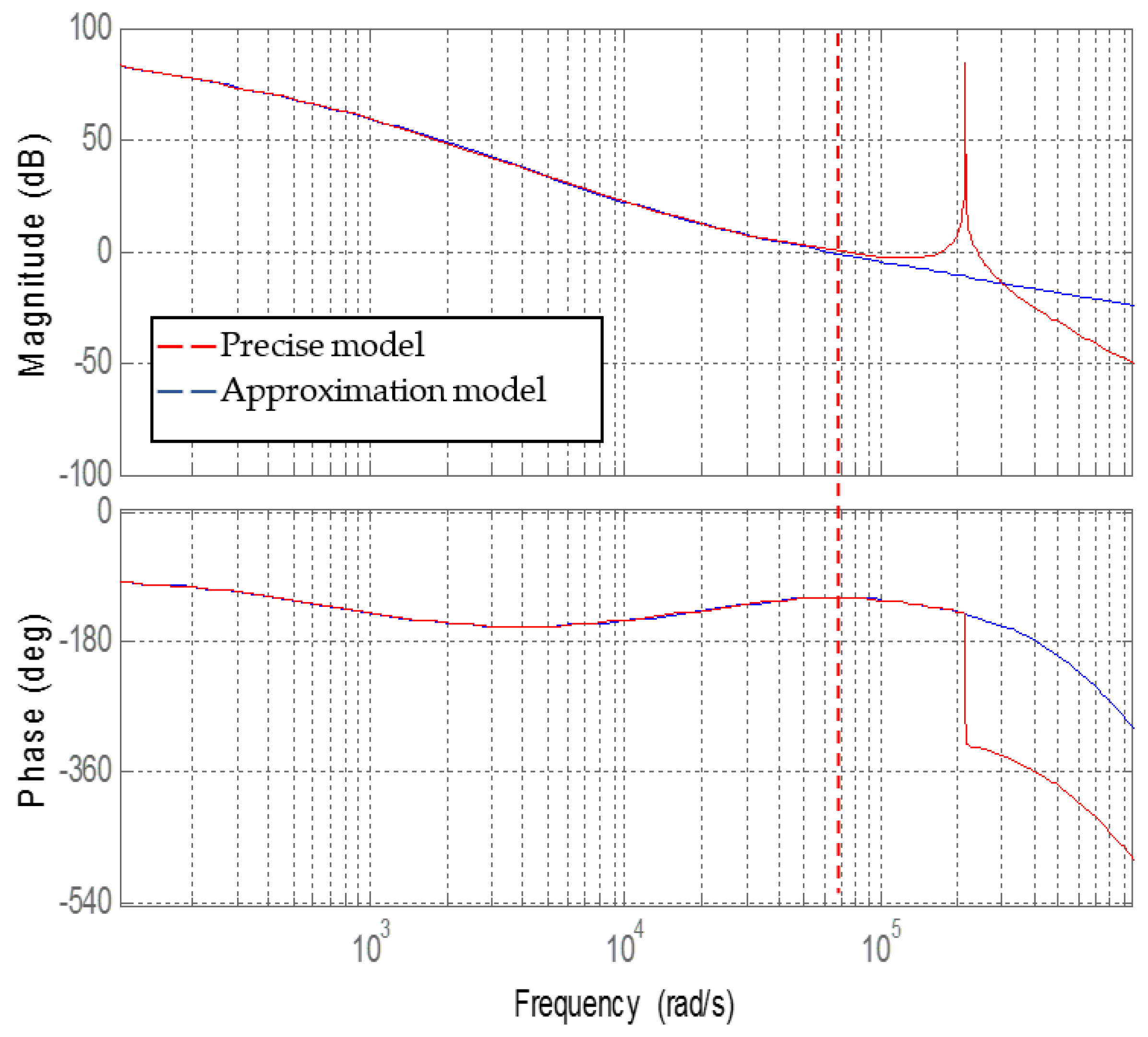
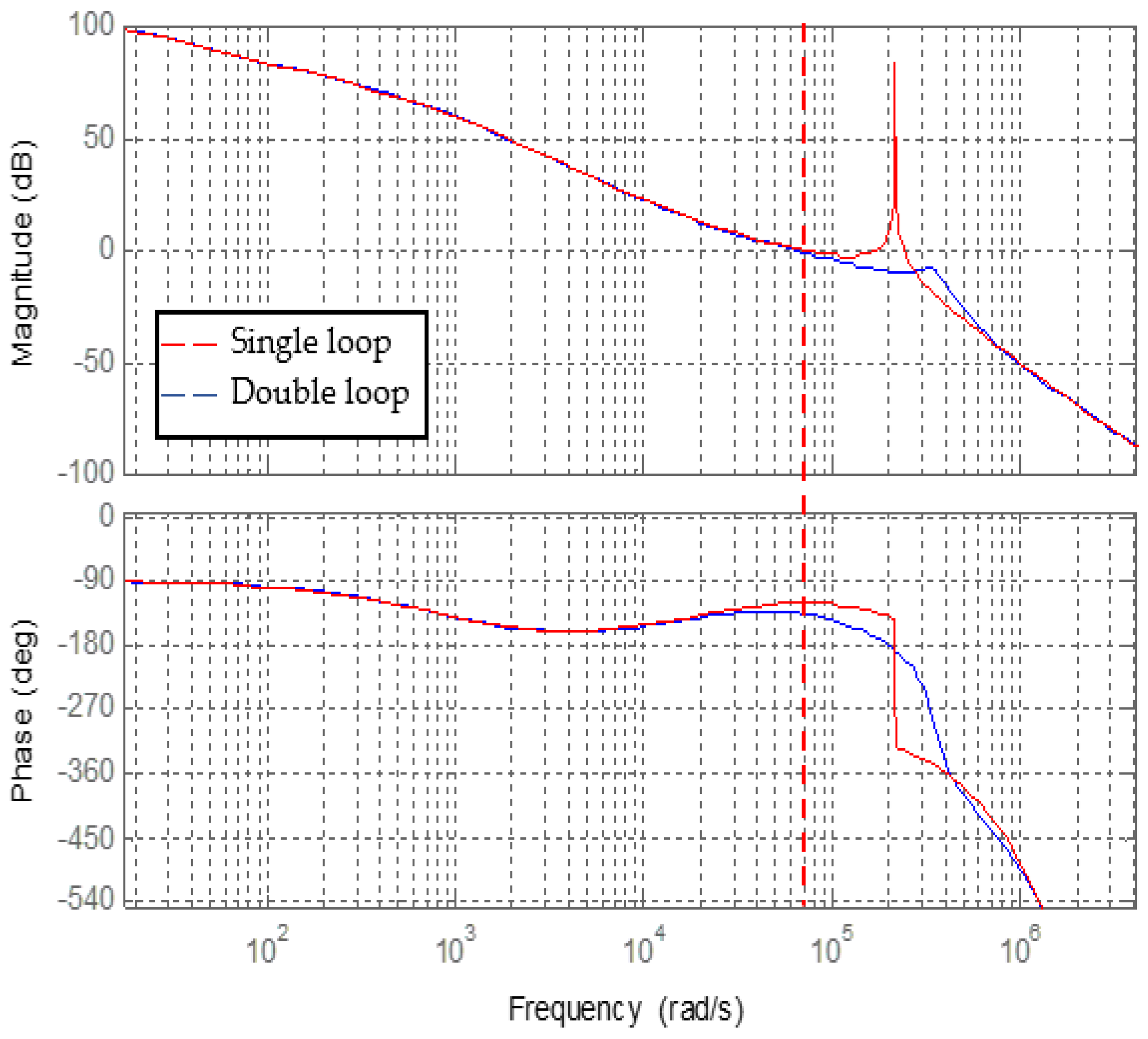
4.3. Capacitor Current Feedback Design

In Section 4.2, the influence of filter capacitor is neglected when the PI parameters are designed. However, the LC filter together with the load inductance forms the LCL filter, which leads to resonance. To analyze the stability of the ARSI, the influence of filter capacitor cannot be ignored. The filter capacitor current feedback is introduced to damp the resonance.
Because of the delay caused by the computation, the system is no longer a minimum phase system. To design the inner capacitor current loop, a discrete model must be built instead of a continuous model. Figure 10 shows the model of the inverter, which is obtained from Figure 6.
The closed-loop and open-loop transfer functions can be obtained as follows. (The detailed proof is presented in Appendix A.)
T ( z ) = i o ( z ) i o * ( z ) = G d c ( z ) G c ( z ) G P ( z ) 1 + K c f G d c ( z ) G T ( z ) + G d c ( z ) G c ( z ) G P ( z )
G ( z ) = i o ( z ) i o * ( z ) i o ( z ) = G d c ( z ) G c ( z ) G P ( z ) 1 + K c f G d c ( z ) G T ( z ) ,
where
G c ( z ) = K p + K i 1 z 1
G d c ( z ) = z 1
G T ( z ) = K p w m C f L f ( z 1 ) sin φ z 2 2 z cos φ + 1
G P ( z ) = K p w m z ( R o F cos φ + L o ω r e s F sin φ R o F ) + R o F R o F cos φ + L o ω r e s F sin φ z 2 2 z cos φ + 1
F = L f C f L o 2 + L f C f R o 2
φ = ω r e s T s p
ω r e s = 1 L f C f .
In the z-domain, the root locus is used to analyze the stability of the system. The relevant expressions can be developed from Equation (23) as follows:
1 + K c f G d c ( z ) G T ( z ) + G d c ( z ) G c ( z ) G P ( z ) = 0 .
Equation (19) can be transformed as follows:
1 + K c f G d c ( z ) G c ( z ) 1 + G d c ( z ) G c ( z ) G P ( z ) = 0 .
From Equation (26), the root locus related to Kcf can be plotted in Figure 11. When the capacitor current feedback is not used, namely Kcf = 0, the closed-loop poles are outside the unit circle, which demonstrates that the system is unstable. As Kcf increases, the system becomes stable. However, if Kcf is too large, the system becomes unstable again.
Figure 12 shows the Bode plot with different Kcf which is obtained from Equation (24). In the magnitude-frequency characteristic, Kcf hardly influences the low-frequency characteristic. As Kcf increases, the open-loop gain decreases slightly around the crossover frequency ωc. Besides, the resonance peak is damped. In the phase-frequency characteristic, the phase margin decreases with the increase of Kcf. When Kcf is large enough, the phase-frequency curve crosses −180° after it drops to −180°. This makes the system unstable according to the stability criterion.
In order to stabilize the system, the active damping gain Kcf must meet the requirements as follows. (The detailed proof is presented in Appendix B.)
K c f min 1 < K c f < K c f max 1   and   K c f min 2 < K c f < K c f max 2 ,
where
K c f min 1 = 1 cos φ + K p w m L o ω r e s F sin φ K p w m C f L f sin φ
K c f max 1 = 1 + cos φ K p K p w m F ( R o cos φ R o 2 L o ω r e s sin φ ) 2 K p w m C f L f sin φ
K c f min 2 = 1 2 cos φ 2 K p K p w m F ( R o R o cos φ + L o ω r e s sin φ ) + ( 1 2 cos φ ) 2 4 + K p K p w m ( 2 R o F cos φ 2 R o F ) K p w m C f L f sin φ
K c f max 2 = 1 2 cos φ 2 K p K p w m F ( R o R o cos φ + L o ω r e s sin φ ) ( 1 2 cos φ ) 2 4 + K p K p w m ( 2 R o F cos φ 2 R o F ) K p w m C f L f sin φ .

5. Design Example

The circuit parameters are listed in Table 2. The specifications are given as the crossover frequency fc ≈ 10 kHz and the phase margin φm > 45°.
(1) Determination of the initial resonant current Ir:
According to Equation (1), the minimum initial resonant current is given as Ir_min > 2.16 A. The minimum initial resonant current and the initial resonant current for AZVS are selected as Ir_min = 2.5 A and Ir_A = 5 A, respectively. Therefore, when iLf_l < −2.5 A, Sr1 is not operated, achieving NZVS of S1 and S4 according to Table 1. Otherwise, Sr1 would be turned on properly to realize AZVS of S1 and S4. Regarding S2 and S3, when iLf_u < 2.5 A, Sr2 must be turned on to create AZVS conditions. When iLf_u > 2.5 A, S2 and S3 can achieve NZVS.
(2) Determination of the upper limit and lower limit of the DPWM (Vupperlimit and Vlowerlimit)
The frequency of the DPWM clock is 120 MHz. Thus, the carriers are specified as Vcmax = 300 and Vcmin = 0 to achieve 200 kHz switching frequency. To simplify the calculation, the filter inductor current ripple is neglected. Therefore, the maximum required auxiliary current can be obtained from Equation (5) as ILrm_max = Ir_A + Io_max = 13 A. The maximum charging time tch_max can be calculated from Equation (6) as tch_max = 357.5 ns. The upper limit can be calculated from Equation (12) as Vupperlimit ≈ 266 by using the improved loading scheme. Thus, the lower limit Vlowerlimit and maximum duty ratio Dmax are 34 and 0.867, respectively. Regarding the conventional loading scheme, the upper limit, lower limit, and maximum duty ratio are 257, 43, and 0.857, respectively. Table 3 shows a comparison of the parameters between the conventional and improved loading scheme. The range of the duty ratio is improved by utilizing the improved loading scheme.
(3) Determination of the PI regulator parameters and active damping gain Kcf
The active damping gain Kcf will influence the stability of the system and the phase margin will decrease due to the increase of Kcf according to the analysis in Section 4.3. However, the influence of the filter capacitor is neglected to simplify the design of the PI regulator in Section 4.2. Therefore, in order to meet the requirement φm > 45°, the phase margin is specified as 60° due to the capacitor current feedback. Thus, the parameters of the PI regulator can be calculated from Equation (21). The results are that Kp = 3.6522 and Ki = 70,999. To ensure the system’s stability, the capacitor current feedback gain Kcf must meet the requirement of 0.0158 < Kcf < 0.119 according to Equation (27). The feedback gain is selected as Kcf = 0.05.
Based on the above parameters, the Bode plots of the single loop and double loop can be obtained from Figure 13. The crossover frequency of the single loop is −62,900 rad/s and the phase margin is 60°. This is in agreement with the design specifications. However, the LC filter leads to resonance, which makes the phase–frequency curve cross −180° after it drops to −180°. According to the stability criterion, the single-loop system is unstable.
Regarding the double-loop control, the crossover frequency is −61,000 rad/s and the phase margin is 46.4°. Due to the capacitor current feedback, the crossover frequency and the phase margin decrease slightly. However, this outcome meets the requirement fc ≈ 10 kHz and φm > 45°. When 20 log | G ( j ω ) | 0 , the phase–frequency curve does not cross −180°. According to the stability criterion, the double-loop system is stable.

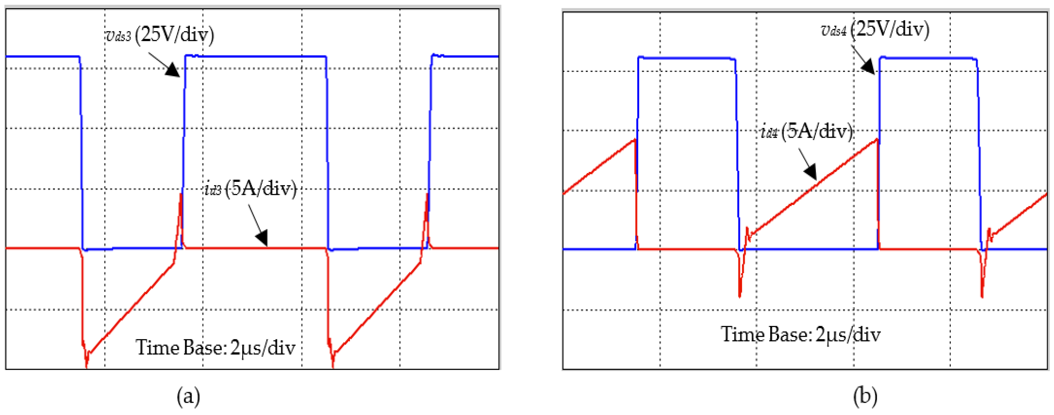
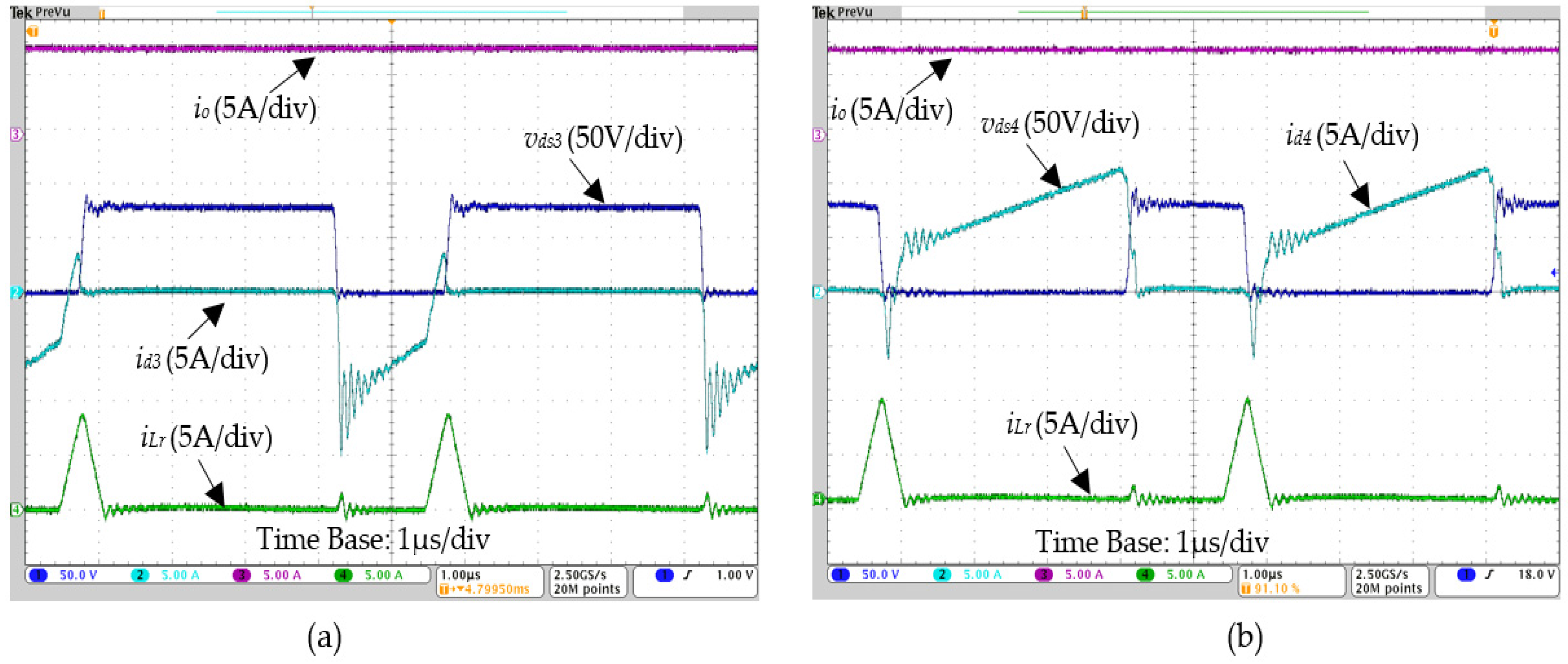
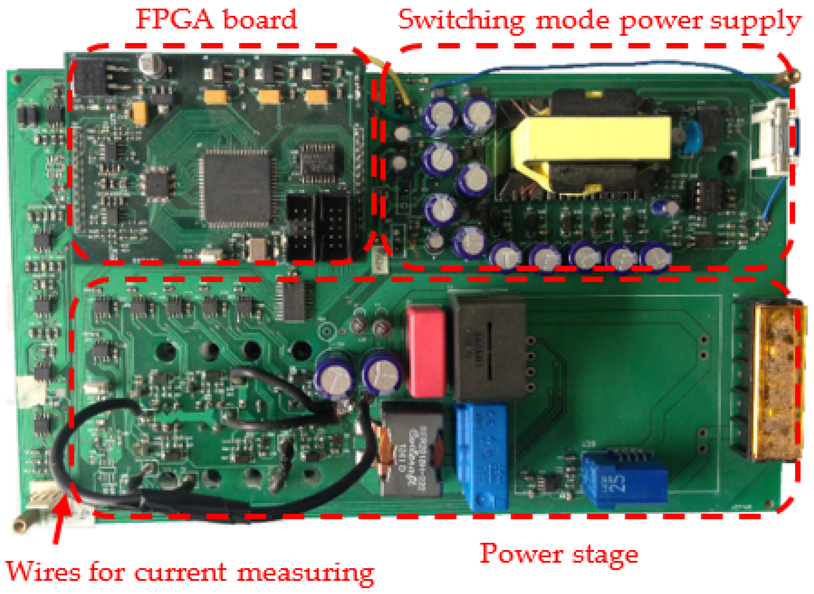
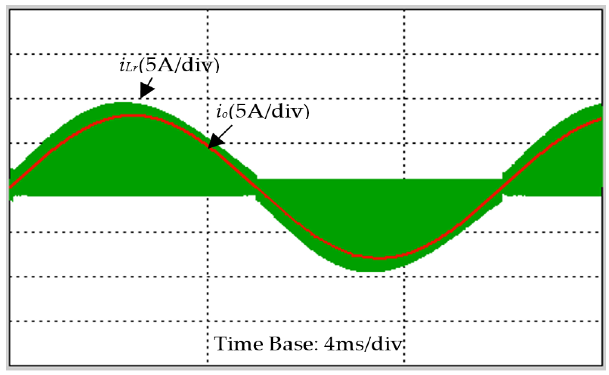
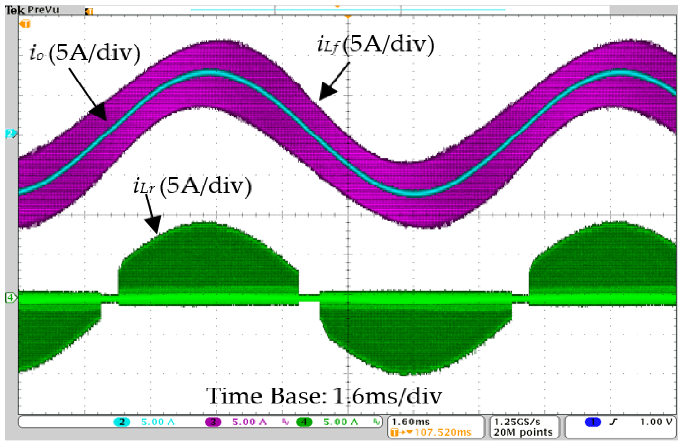
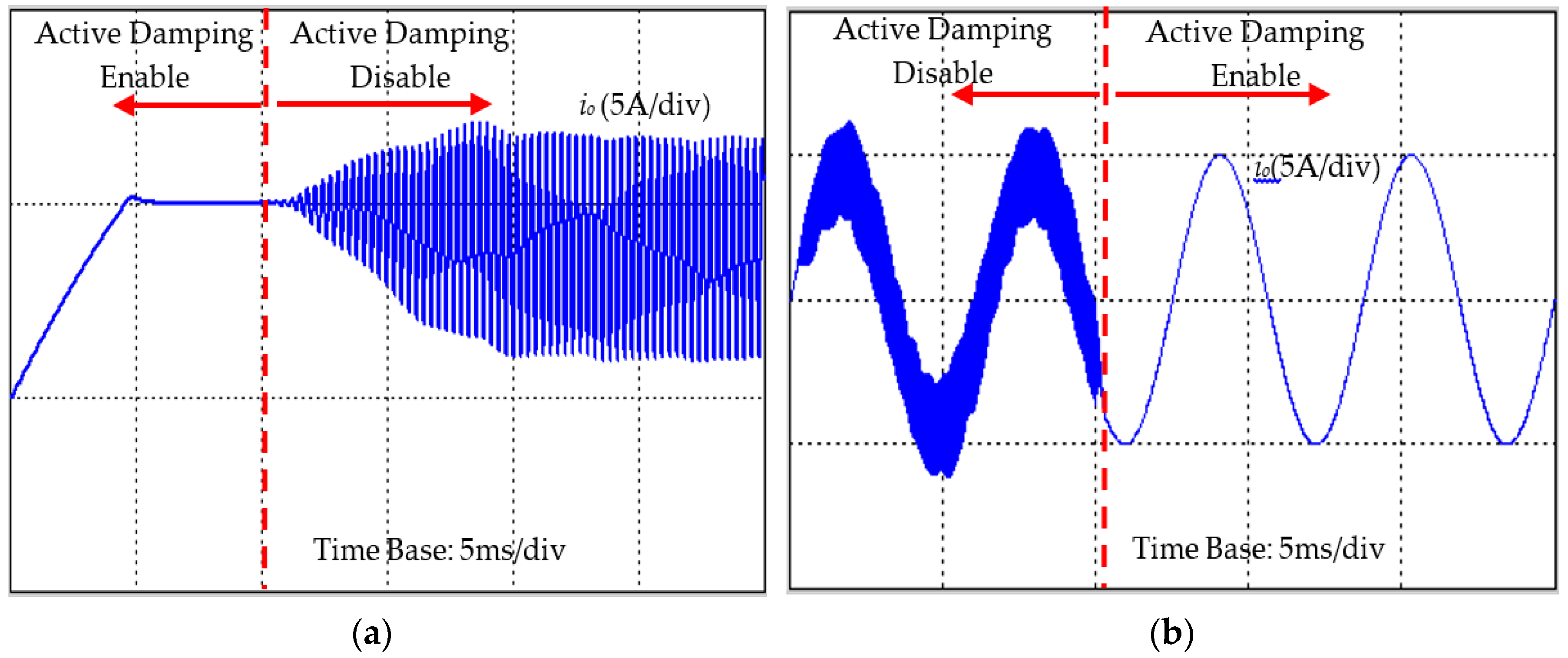
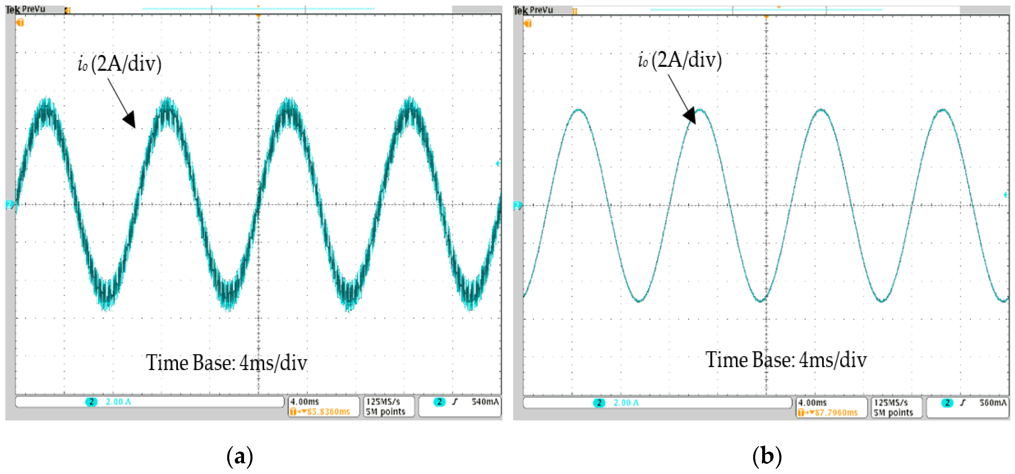
6. Simulations and Experiments

The method was implemented in the Altera Cyclone IV FPGA with the parameters given in Table 2. Figure 14 shows a photograph of the prototype. It consists of a FPGA (EP4CE22E22C7N, Altera Corporation, San Jose, CA, USA) control board, a switching power supply, a MOSFET driver, and a power circuit. The method is verified in the simulation using Saber.
Figure 15 and Figure 16 show the simulation and experimental transitional waveforms of the main switches, respectively. During the turn-on commutation, the drain currents id3 and id4 begin increasing after the drain-source voltage vds3 and vds4 drop to zero. ZVS of S4 is achieved with the operation of Sr1, whereas the auxiliary switches are not turned on to achieve ZVS of S3. Regarding the turn-off commutation, the drain current overlaps the drain-source voltage slightly because the resonant capacitance is not large enough. Due to the parasitic components, ringing occurs during the commutation in the experiment.
Figure 17 and Figure 18 show the simulation and experimental waveforms of the auxiliary current with an 8 A, 100 Hz sinusoidal output current. The peak auxiliary switch current follows the load current with clear load adaptability. It can be seen that the lower the load current, the lower the auxiliary current.
Figure 19 and Figure 20 show the simulation and experimental results of the output current with and without active damping method, respectively. Figure 19 demonstrates that strong resonance occurs in the output current without the active damping method, because closed-loop poles are outside the unit circle shown in Figure 11. After utilizing the capacitor current feedback, the poles can be moved into the unit circle. Therefore, the system can be stable both at the DC or sinusoidal output current conditions. Figure 20 also demonstrates that active damping is necessary to maintain stability and current quality.
Figure 21 and Figure 22 show the simulation and experimental results of the load dynamic response, respectively. The results demonstrate that the output current tracks the reference current quickly. However, a bit of overshot exists in the transient response.

7. Conclusions

In some high-performance applications, an LC filter must be added to the auxiliary resonant snubber inverter (ARSI) to reduce the output current ripple. This makes the system quite different to the conventional ARSI without LC filter. This paper presents the modeling and the double-loop digital control of the ARSI with LC filter. The following points can be summarized to cover the paper:
(1)
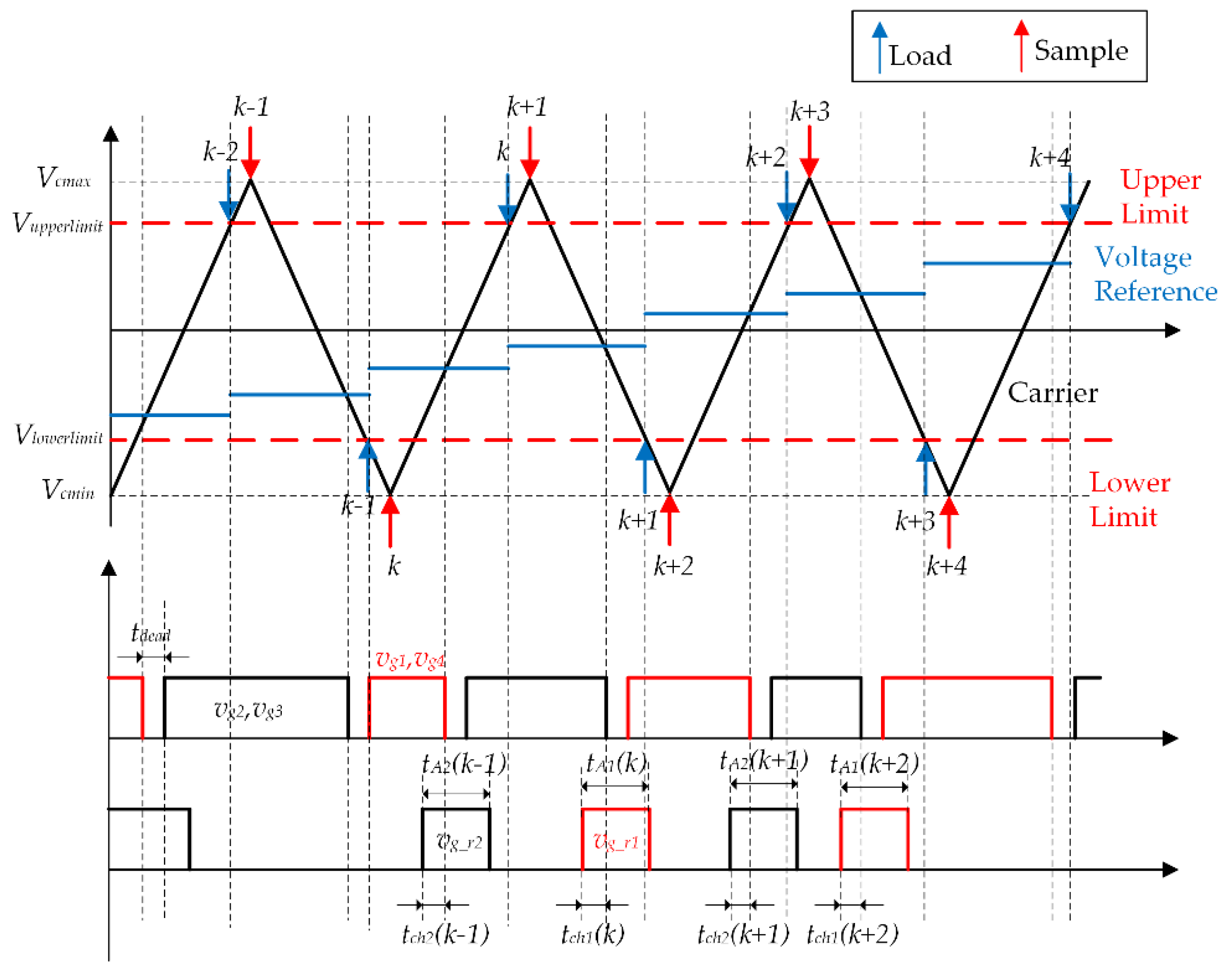
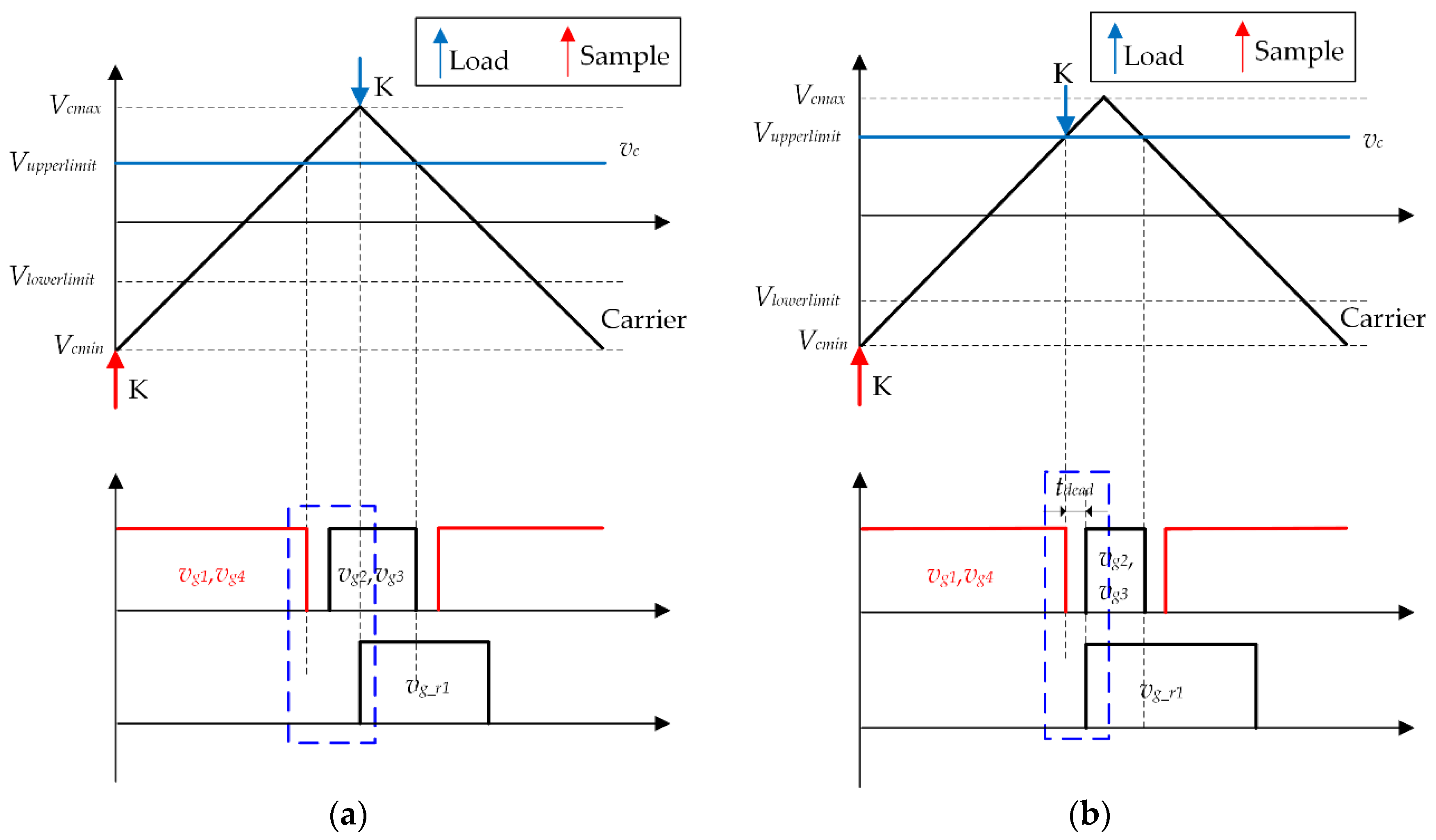
An improved loading scheme that the data is updating at the upper limit and lower limit of the carrier is proposed to improve the maximum duty ratio.
(2)
The filter capacitor current feedback is introduced to damp the resonance caused by the LC filter.
(3)
A step-by-step digital controller design method, including the auxiliary current controller and the output PI controller, is proposed, in which the computation and transport delay is considered.
The control method has been verified by simulations and experiments. The maximum duty ratio is improved by 0.01 with the proposed loading method. In addition, soft-switching can be realized for the entire load range. Also, the resonance can be eliminated with the capacitor current feedback.

Acknowledgments

This work was supported by the State Key Program of National Natural Science of China under Grant 51537002 and the National Natural Science Foundation of China under Grant 51607044.

Author Contributions

Hailin Zhang conceived the proposed method and wrote the paper; Baoquan Kou provided technical guidance and advice for the manuscript; Lu Zhang and Yinxi Jin performed the experiments and reviewed the manuscript.

Conflicts of Interest

The authors declare no conflict of interest.

Appendix A

From Figure 10, the capacitor current feedback Kcficf(z) and the output current io(z) to the voltage ve(z) can be written as follows:
K c f i c f ( z ) v e ( z ) = K p w m K c f G d c ( z ) G T ( z )
i o ( z ) v e ( z ) = K p w m K c f G d c ( z ) G P ( z )
v e ( z ) = [ i o * ( z ) i o ( z ) ] G c ( z ) K c f i c f ( z ) .
From Equations (A1)–(A3), the closed-loop and open-loop transfer function, respectively, can be obtained as follows:
T ( z ) = i o ( z ) i o * ( z ) = G d c ( z ) G c ( z ) G P ( z ) 1 + K c f G d c ( z ) G T ( z ) + G d c ( z ) G c ( z ) G P ( z )
G ( z ) = i o ( z ) i o * ( z ) i o ( z ) = G d c ( z ) G c ( z ) G P ( z ) 1 + K c f G d c ( z ) G T ( z ) .
Applying z-transformation to GT(s), GT(z) can be obtained as follows:
G T ( z ) = Z [ K p w m H ( s ) G 1 ( s ) ] = K p w m C f L f ( z 1 ) sin φ z 2 2 z cos φ + 1 ,
where
φ = ω r e s T s p   and   ω r e s = 1 L f C f .
Commonly, because Tsp << Lo/Ro, e R o L o T s p 1 . Therefore, applying z-transformation to GP(s), GP(z) can be obtained as follows:
G P ( z ) = Z [ K p w m H ( s ) G 1 ( s ) G 2 ( s ) ] K p w m z ( R o F cos φ + L o ω r e s F sin φ R o F ) + R o F R o F cos φ + L o ω r e s F sin φ z 2 2 z cos φ + 1 ,
where
F = L f C f L o 2 + L f C f R o 2 .

Appendix B

Equation (25) can be simplified as follows:
z 3 z · 2 cos φ + a z + b = 0 ,
where
a = 1 + K c f K p w m C f L f sin φ K p K p w m F ( R o cos φ + L o ω r e s sin φ R o )
b = K c f K p w m C f L f sin φ + K p K p w m F ( R o R o cos φ + L o ω r e s sin φ ) .
In order to easily identify the quantity of the unstable poles, w-transform z = (1 + w)/(1 + w) is introduced. Therefore, Equation (B1) can be transformed as follows:
a 3 w 3 + a 2 w 2 + a 1 w + a 0 = 0 ,
where
{ a 3 = 1 + 2 cos φ + a b a 2 = 3 + 2 cos φ a + 3 b a 1 = 3 2 cos φ a 3 b a 0 = 1 2 cos φ + a + b .
It can be obtained that a0 > 0. Thus according to Routh’s Method, the following requirement must be satisfied to maintain the system’s stability:
{ a 3 > 0 a 2 > 0 a 2 a 1 a 3 a 0 a 2 > 0 a 0 > 0 .
From Equation (B3), the filter capacitor current feedback gain Kcf must meet the following requirement:
K c f min 1 < K c f < K c f max 1   and   K c f min 2 < K c f < K c f max 2 ,
where
K c f min 1 = 1 cos φ + K p w m L o ω r e s F sin φ K p w m C f L f sin φ
K c f max 1 = 1 + cos φ K p K p w m F ( R o cos φ R o 2 L o ω r e s sin φ ) 2 K p w m C f L f sin φ
K c f min 2 = 1 2 cos φ 2 K p K p w m F ( R o R o cos φ + L o ω r e s sin φ ) + ( 1 2 cos φ ) 2 4 + K p K p w m ( 2 R o F cos φ 2 R o F ) K p w m C f L f sin φ
K c f max 2 = 1 2 cos φ 2 K p K p w m F ( R o R o cos φ + L o ω r e s sin φ ) ( 1 2 cos φ ) 2 4 + K p K p w m ( 2 R o F cos φ 2 R o F ) K p w m C f L f sin φ .

References

  1. Schmidt, R.M.; Schitter, G.; Eijk, J. The Design of High Performance Mechatronics; Delft University Press: Amsterdam, The Netherlands, 2011; pp. 438–444. [Google Scholar]
  2. Charalambous, A.; Yuan, X.; McNeill, N.; Yan, Q.Z. EMI reduction with a soft-switched auxiliary commutated pole inverter. In Proceedings of the IEEE Energy Conversion Congress and Exposition, Montreal, QC, Canada, 20–24 Septemper 2015; pp. 2650–2657.
  3. Beltrame, R.C.; Rakoski Zientarski, J.R.; da Silva Martins, M.L.; Pinheiro, J.R.; Hey, H.L. Simplified zero-voltage-rransition circuits applied to bidirectional poles: Concept and synthesis methodology. IEEE Trans. Power Electron. 2011, 26, 1765–1776. [Google Scholar] [CrossRef]
  4. Russi, J.L.; da Silva Martins, M.L.; Schuch, L.; Pinheiro, J.R.; Hey, H.L. Synthesis methodology for multipole ZVT converters. IEEE Trans. Ind. Electron. 2007, 54, 1783–1795. [Google Scholar] [CrossRef]
  5. McMurray, W. Resonant snubbers with auxiliary switches. IEEE Trans. Ind. Appl. 1993, 29, 355–362. [Google Scholar] [CrossRef]
  6. DeDonker, R.W.; Lyons, J.P. The auxiliary resonant commutated pole converter. In Proceedings of the Industry Applications Society Annual Meeting, Seattle, WA, USA, 7–12 October 1990; pp. 1228–1235.
  7. Lai, J.S. Resonant snubber-based soft-switching inverters for electric propulsion drives. IEEE Trans. Ind. Electron. 1997, 44, 71–80. [Google Scholar]
  8. Lai, J.S.; Young, R.W.; Ott, G.W.; McKeever, J.W.; Peng, F.Z. A delta-configured auxiliary resonant snubber inverter. IEEE Trans. Ind. Appl. 1996, 32, 518–525. [Google Scholar]
  9. Yuan, X.; Barbi, I. Analysis, designing, and experimentation of a transformer-assisted PWM zero-voltage switching pole inverter. IEEE Trans. Power Electron. 2000, 15, 950–950. [Google Scholar]
  10. Russi, J.L.; da Silva Martins, M.L.; Hey, H.L. Coupled-filter-inductor soft-switching techniques: Principles and topologies. IEEE Trans. Ind. Electron. 2008, 55, 3361–3373. [Google Scholar] [CrossRef]
  11. Yu, W.; Lai, J.; Park, S. An improved zero-voltage switching inverter using two coupled magnetics in one resonant pole. IEEE Trans. Power Electron. 2010, 25, 952–961. [Google Scholar]
  12. Hanigovszki, N.; Poulsen, J.; Blaabjerg, F. A Novel Output Filter Topology to Reduce Motor Overvoltage. IEEE Trans. Ind. Appl. 2004, 40, 845–852. [Google Scholar] [CrossRef]
  13. Wu, W.; He, Y.; Tang, T.; Blaabjerg, F. A New Design Method for the Passive Damped LCL and LLCL Filter-Based Single-Phase Grid-Tied Inverter. IEEE Trans. Ind. Electron. 2013, 60, 4339–4350. [Google Scholar] [CrossRef]
  14. Balasubramanian, A.K.; John, V. Analysis and design of split-capacitor resistive-inductive passive damping for LCL filters in grid-connected inverters. IET Power Electron. 2013, 6, 1822–1832. [Google Scholar] [CrossRef]
  15. Xin, Z.; Loh, P.C.; Wang, X.; Blaabjerg, F.; Tang, Y. Highly Accurate Derivatives for LCL-Filtered Grid Converter with Capacitor Voltage Active Damping. IEEE Trans. Power Electron. 2016, 31, 3612–3625. [Google Scholar] [CrossRef]
  16. Dannehl, J.; Fuchs, F.W.; Hansen, S.; Thøgersen, P.B. Investigation of Active Damping Approaches for PI-Based Current Control of Grid-Connected Pulse Width Modulation Converters with LCL Filters. IEEE Trans. Ind. Appl. 2010, 46, 1509–1517. [Google Scholar] [CrossRef]
  17. Wagner, M.; Barth, T.; Alvarez, R.; Ditmanson, C.; Bernet, S. Discrete-Time Active Damping of LCL-Resonance by Proportional Capacitor Current Feedback. IEEE Trans. Ind. Appl. 2014, 50, 3911–3920. [Google Scholar] [CrossRef]
  18. Parker, S.G.; McGrath, B.P.; Holmes, D.G. Regions of Active Damping Control for LCL Filters. IEEE Trans. Ind. Appl. 2014, 50, 424–432. [Google Scholar] [CrossRef]
  19. Dong, W.; Yu, H.; Lee, F.C.; Lai, J. Generalized concept of load adaptive fixed timing control for zero-voltage-transition inverters. In Proceedings of the IEEE Applied Power Electronics Conference and Exposition, Anaheim, CA, USA, 4–8 March 2001; pp. 179–185.
  20. Chan, C.C.; Chau, K.T.; Chan, D.T.W.; Yao, J.; Lai, J.S.; Li, Y. Switching characteristics and efficiency improvement with auxiliary resonant snubber based soft-switching inverters. In Proceedings of the IEEE Power Electronics Specialists Conference, Fukuoka, Japan, 17–22 May 1998; pp. 429–435.
  21. Kou, B.; Zhang, H.; Jin, Y.; Zhang, H. An Improved Control Scheme for Single-Phase Auxiliary Resonant Snubber Inverter. In Proceedings of the IEEE 8th International Power Electronics and Motion Control Conference, Hefei, China, 22–26 May 2016; pp. 1259–1263.
  22. Holmes, D.G.; Lipo, T.A. Pulse Width Modulation for Power Converters: Principles and Practice; IEEE Press: New York, NY, USA, 2003; pp. 105–120. [Google Scholar]
  23. Kong, W.Y.; Holmes, D.G.; McGrath, B.P. Enhanced Three Phase AC Stationary Frame PI Current Regulators. In Proceedings of the IEEE Energy Conversion Congress and Exposition, San Jose, CA, USA, 20–24 September 2009; pp. 83–90.
  24. Agorreta, J.L.; Borrega, M.; López, J.; Marroyo, L. Modeling and control of N-paralleled grid-connected inverters with LCL filter coupled due to grid impedance in PV plants. IEEE Trans. Power Electron. 2011, 26, 770–785. [Google Scholar] [CrossRef]
  25. Buso, S.; Mattavelli, P. Digital Control in Power Electronics; Morgan & Claypool: Seattle, WA, USA, 2006; pp. 13–57. [Google Scholar]
Figure 1. Circuit of the single-phase auxiliary resonant snubber inverter (ARSI) with LC filter.
Applsci 06 00377 g001
Figure 2. Control diagram of the ARSI.
Applsci 06 00377 g002
Figure 3. Key waveforms to realize the zero-voltage switching (ZVS) of S1 and S4 (a) iLf_l < −Ir_min; (b) iLf_l > −Ir_min.
Applsci 06 00377 g003
Figure 4. Digital pulse-width-modulation (DPWM) diagram of the ARSI.
Applsci 06 00377 g004
Figure 5. DPWM diagram at the condition of Io_max and Dmax: (a) conventional loading scheme; (b) improved loading scheme.
Applsci 06 00377 g005
Figure 6. Digital control model of the output current controller.
Applsci 06 00377 g006
Figure 7. Output current controller model in the s-domain.
Applsci 06 00377 g007
Figure 8. Bode plot of the approximated model and the precise model.
Applsci 06 00377 g008
Figure 9. Bode plot of the ARSI with different PI parameters: (a) different Kp; (b) different Ki.
Applsci 06 00377 g009
Figure 10. Model of ARSI in digital control.
Applsci 06 00377 g010
Figure 11. Root locus of variation in active damping gain Kcf using a dual-loop controller.
Applsci 06 00377 g011
Figure 12. Open-loop Bode plot with different active damping gain Kcf.
Applsci 06 00377 g012
Figure 13. Bode plot of the single loop and double loop.
Applsci 06 00377 g013
Figure 14. Photograph of the prototype.
Applsci 06 00377 g014
Figure 15. Simulation results of the current and voltage of the main switches when io = 8 A. (a) S3; (b) S4.
Applsci 06 00377 g015
Figure 16. Experimental results of the current and voltage of the main switches when io = 8 A. (a) S3; (b) S4.
Applsci 06 00377 g016
Figure 17. Simulation waveforms of the auxiliary current with an 8 A, 100 Hz sinusoidal output current.
Applsci 06 00377 g017
Figure 18. Experimental waveforms of the auxiliary current with an 8 A, 100 Hz sinusoidal output current.
Applsci 06 00377 g018
Figure 19. Simulation results of the output current with and without active damping method: (a) DC output current; (b) sinusoidal output current.
Applsci 06 00377 g019
Figure 20. Experimental results of the output current (a) without and (b) with active damping method.
Applsci 06 00377 g020
Figure 21. Simulation results of the load dynamic response: (a) a step change from 12.5% to 75% rated output power; (b) a step change from 75% to 12.5% rated output power.
Applsci 06 00377 g021
Figure 22. Experimental results of the load dynamic response: (a) a step change from 12.5% to 62.5% rated output power; (b) a step change from 62.5% to 12.5% rated output power.
Applsci 06 00377 g022
Table 1. Zero-voltage switching (ZVS) types of switches under different output currents.
SwitchiLf_l < −Ir_miniLf_l > −Ir_minSwitchiLf_u < Ir_miniLf_u > Ir_min
S1 & S4NZVSAZVS (Sr1)S2 & S3AZVS (Sr2)NZVS
Table 2. Parameters of the circuit.
ParameterValue
DC voltage Vs80 V
Switching frequency fs200 kHz
Dead time tdead0.2 μs
Load3.7 Ω, 4.87 mH
Resonant inductor Lr2.2 μH
Resonant capacitor Cr2.7 nF
Filter inductor Lf22 μH
Filter capacitor Cf1 μF
Maximum output current Io_max8 A
Table 3. Comparison of the parameters between the conventional and improved loading scheme.
ParameterConventional Loading SchemeImproved Loading Scheme
Maximum Duty Ratio Dmax0.8570.867
Minimum Duty Ratio Dmin0.1430.133
Upper Limit Vupperlimit257266
Lower Limit Vlowerlimit4334

