1. Introduction
The input data of fuzzy logic controllers (FLC) are usually crisp values that come from different nonlinear physical systems such as Micro Electro Mechanical system (MEMS) glucose microsensors. Therefore a relation is needed to calculate measure inputs or create membership function generators (MFGs). There are many MFGs in forms of voltage to voltage [
1], current to current [
2,
3], voltage to current [
4], and other methods. There are other approaches which used two sources or emitter coupled differential pairs for single membership function in bipolar or MOS technology [
5,
6]. However, the fuzzifier circuit presented by Wilamowski [
7] is simpler and uses one differential pair per membership function, but there is a limitation to adjust the slope of MFs by changing
W/
L ratios manually [
6,
7]. So this is a fundamental problem for an architecture which is aimed to be a programmable FLC chip.
Contrary to conventional structures, our design is capable of tuning the slope of MFs and generating the Gaussian, Trapezoidal, and Triangular forms. These are achieved by changing
W/
L ratios of scaled transistors and choosing different reference voltages using control switches. There are 2
n states to choose arbitrary slopes and type of shapes. This architecture is general purpose for fuzzifier circuits. With a specific purpose, we applied output data of MEMS glucose microsensor to it to introduce fuzzy language terms. Obtained fuzzy data can be processed in fuzzy logic environment using fuzzy rules. Thus a suitable defuzzy (or crisp) output will be obtained to active MEMS micropumps for insulin injection [
8]. Our discussion in this paper will be based on designing new and improved Fuzzifier and C2V convertor circuits. Simulation results are obtained using Hspice and Matlab software.
2. Proposed Fuzzifier Circuit
2.1. Basic Consideration
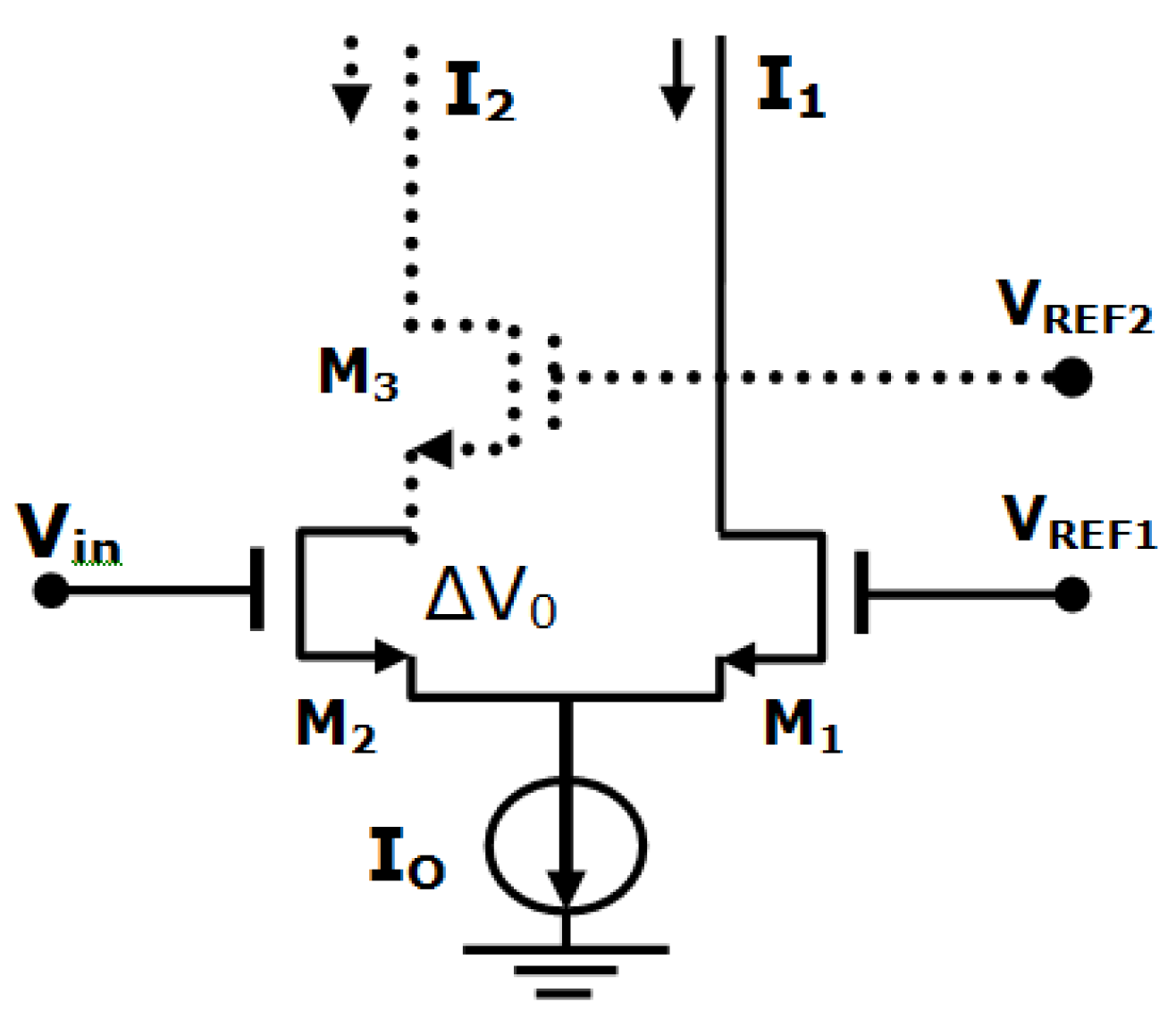
Before analyzing proposed work, let us consider a differential pair and working region to obtain suitable currents. As shown in
Figure 1 and according to the [
6,
7], output currents for introducing MFs in midrange are given by Equation (1):
While on the ends of the input range, the above equation becomes to Equation (2):
where
Vin is the input voltage, VREFi’s are the reference voltages, VTH is the MOS transistor threshold voltage, µCox , Wi/Li are the parameter and size of transistors, and Io is the constant current source.
Figure 1.
Differential pair circuit.
Figure 1.
Differential pair circuit.
On the ends of the input range [
9], this relation can be simplified without
VTH as Equation (3):
where
When
Vin increases, two currents
I1 and
I2 start to descend and ascend for obtaining membership functions. According to Equation (3) and at the point where
Vin =
VREFi , each current becomes as Equation (4):
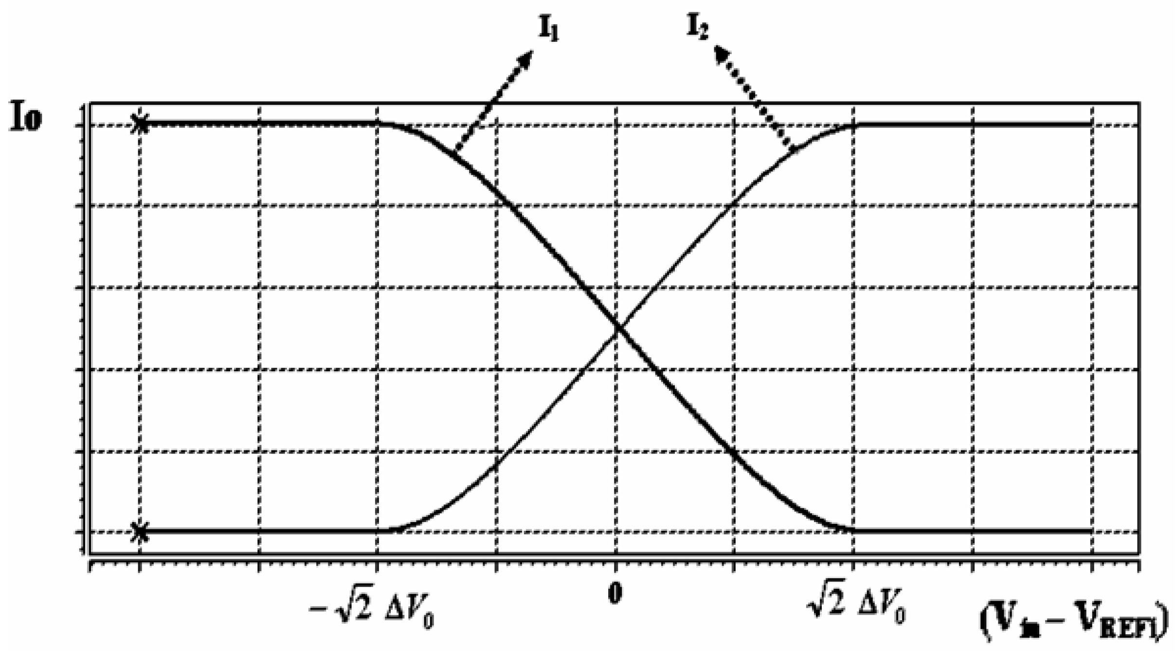
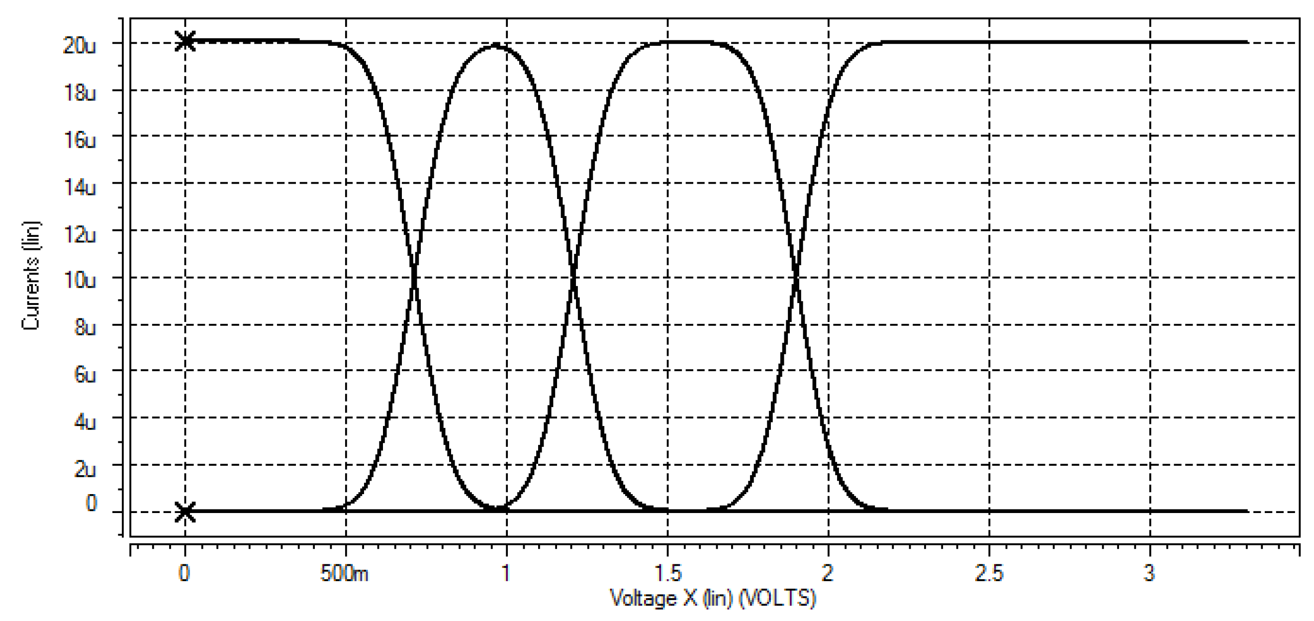
If Vin continues to increase then transistors M1 and M2 enter the cutoff and linear regions respectively. Choosing different reference voltages using control switches cause a change on currents I1 and I2. Also, using different W/L ratios results in changing shape and slope of membership functions.
According to the [
9] and first differential pair of
Figure 1 and then using Equation (3), we can calculate the maximum of (
Vin − V
REFi) as Equation (5):
where:
Therefore the difference √2∆
V0 between
Vin and
VREFi is needed for
I1 and
I2 to be in opposite directions,
i.e., if one of them is max, the other one should be minimum quantity (
Figure 2). According to
Figure 1, if we add transistor M
3 then the voltage of 2√2∆
V0 is needed to have one current in maximum and the other one in minimum quantities,
i.e., this difference voltage is necessary between
VREFi and
VREFi+1 so that: (1) transistor M
1 be in cutoff region to obtain minimum current
I1 and (2) transistor M
2 be in linear region to achieve maximum current
I2.
Figure 2.
Drain current variation of differential pair versus input voltage (Vin − VREFi).
Figure 2.
Drain current variation of differential pair versus input voltage (Vin − VREFi).
The circuit of this basic approach is very flexible and includes equally spaced symmetrical and asymmetrical MFs which can be used in VLSI implementations. For these reasons made some improvements by adding scaled transistors and changing ∆V0’s in constant current. So reduction of ∆V0 causes the enhancement of the number of MFs which will be discussed in the next section.
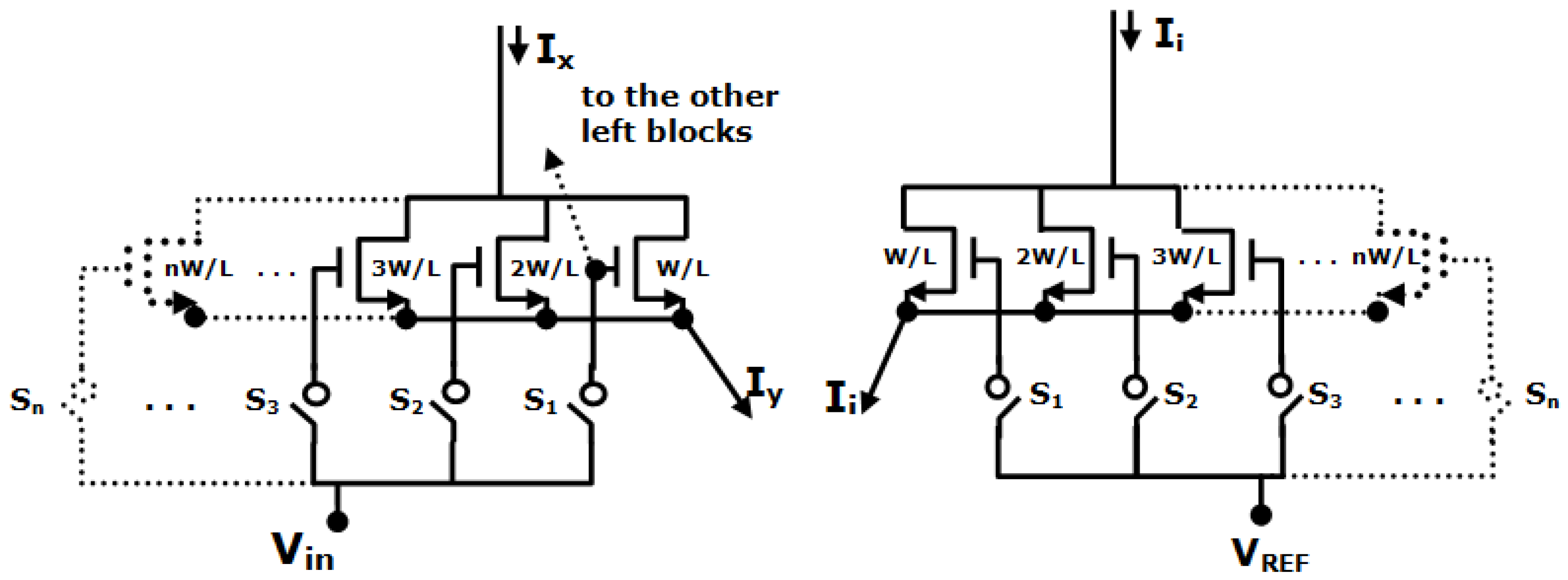
2.2. Main Blocks and Circuits
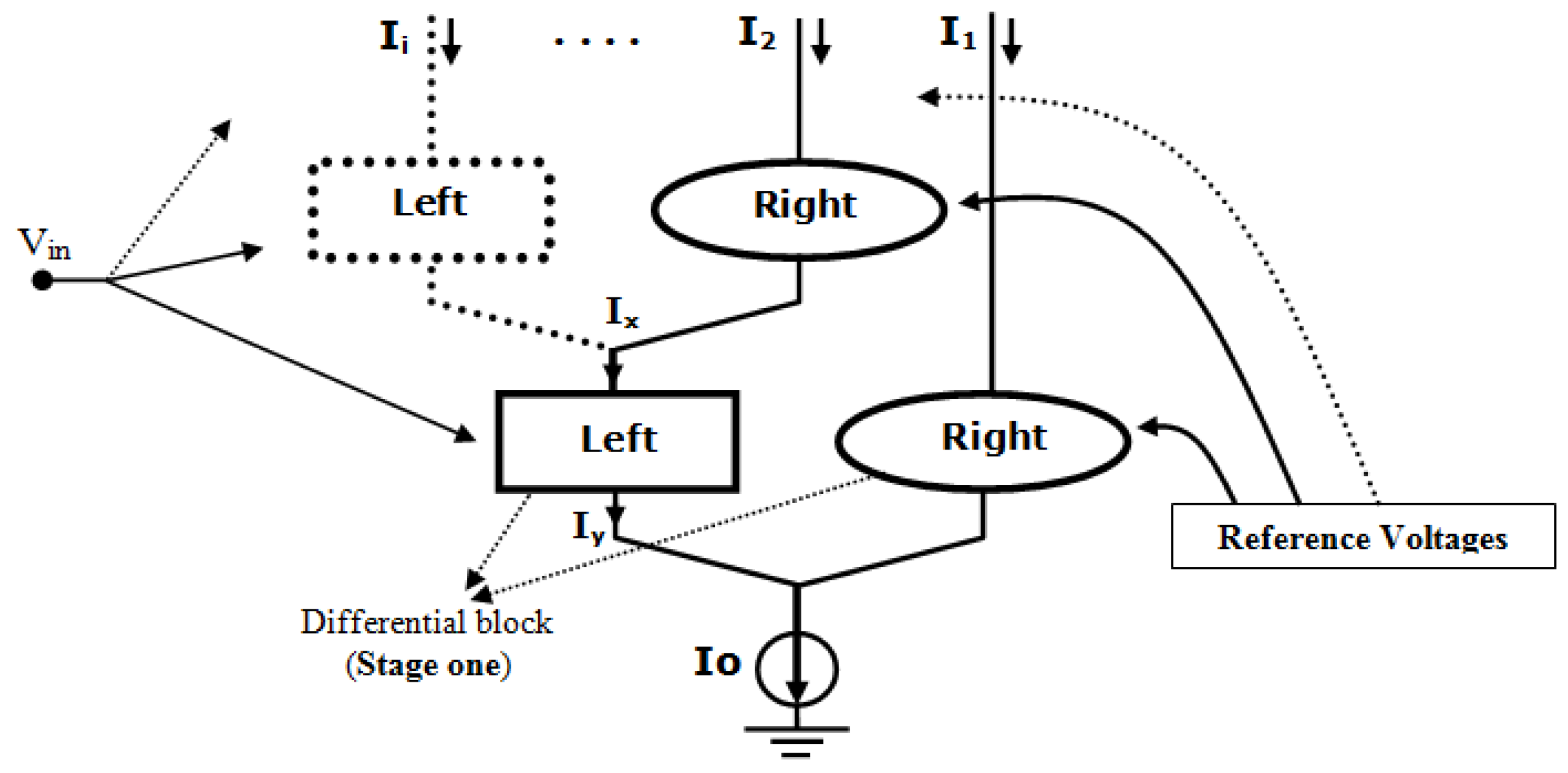
The systematic blocks of proposed Fuzzifier for this purpose are shown in
Figure 3. The improved work is done using differential blocks which consist of transistors that are scaled with a different coefficient of
W/
L’s. In the left column circuit of differential block (
Figure 4) the gates of transistors are connected to (
Vin) either together or alone via control switches. In the same manner,
Figure 4 (right) shows the right circuit of differential block. The scaled transistors in any column of right blocks can be connected to the reference voltage (
VREF) through control switches.
Figure 4.
Left and right circuits for a differential block of fuzzifier stages.
Figure 4.
Left and right circuits for a differential block of fuzzifier stages.
The proposed design has basically a similar operation discussed previously. As we mentioned, increasing
W/
L ratio of scaled transistors cause to decrease ∆
V0 in current constant [
9]. For these reasons the difference voltage of 2√2∆
V0 between two right block
(i) and block
(i+1) would be minimal. This benefit makes it possible to use a lower power supply, high swing, and consequently more stages and numbers of MFs.
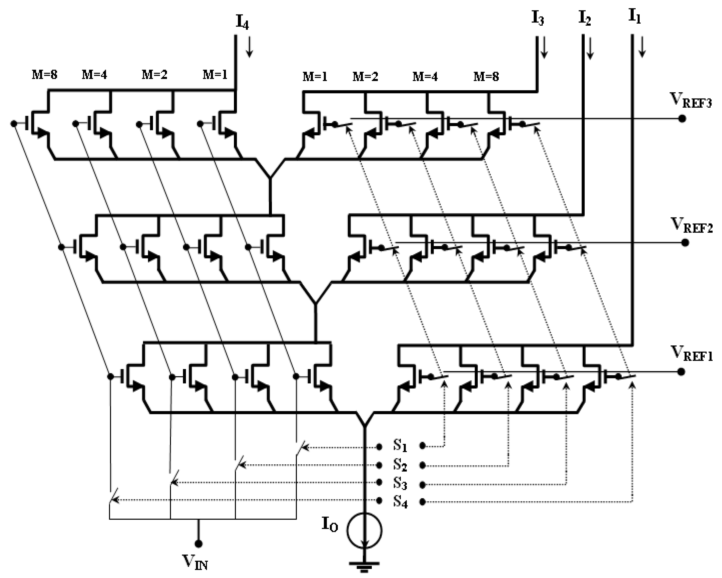
With these results and using the basic of differential pair circuit of
Figure 1 and
Figure 4, the proposed Fuzzifier circuit is completed as shown in
Figure 5. This circuit is capable of obtaining Gaussian membership function shapes with tuning reference voltages in least quantity (
VREF2 −
VREF1 = 2√2∆
V0).
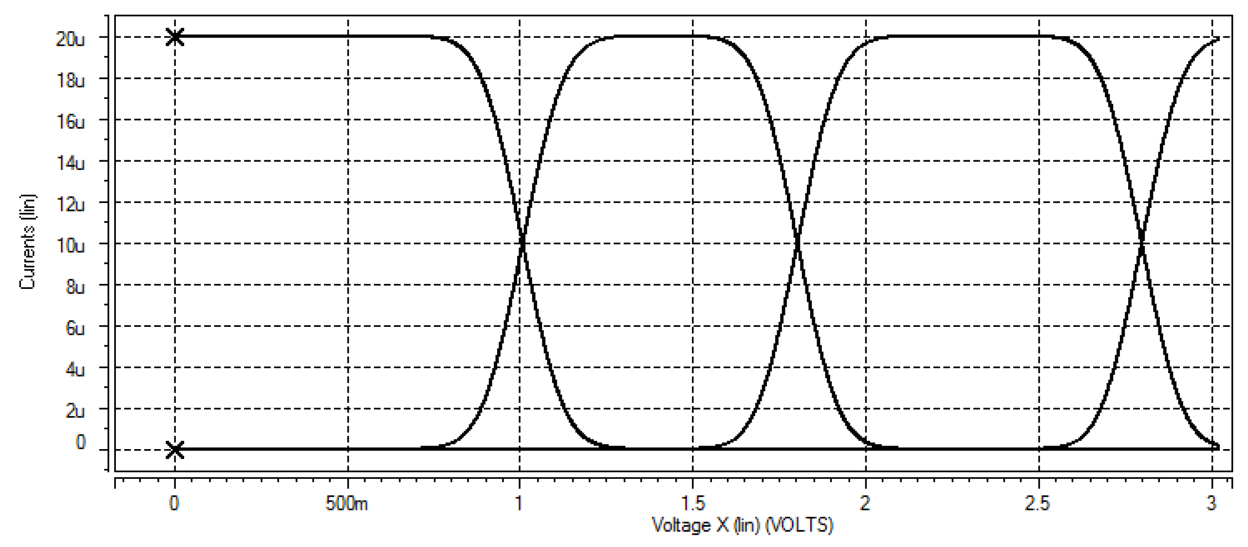
Increasing different reference voltages and distancing them from each other, cause to have Trapezoidal shapes. Different MFs slopes can be achieved by changing transistor sizes in 1, 2, 4, and 8 W/L ratios using control switches. The Triangular membership functions are also resulted with setting different reference voltages in least quantity and using high control switches.
In contrast to conventional works [
1,
10,
11,
12,
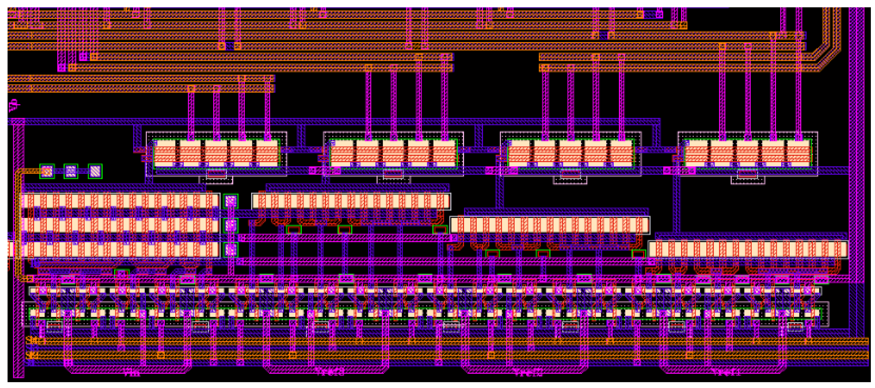
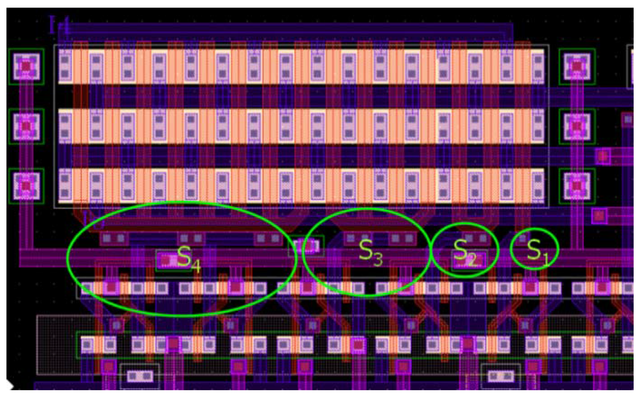
13], the proposed circuit is very simple and flexible in designing Layout (
Figure 6 and
Figure 7) and processing fuzzy data, respectively. It can also generate three different shape types of equally spaced symmetrical membership functions. This work is applicable in VLSI implementations without any complexity and extra hardware.
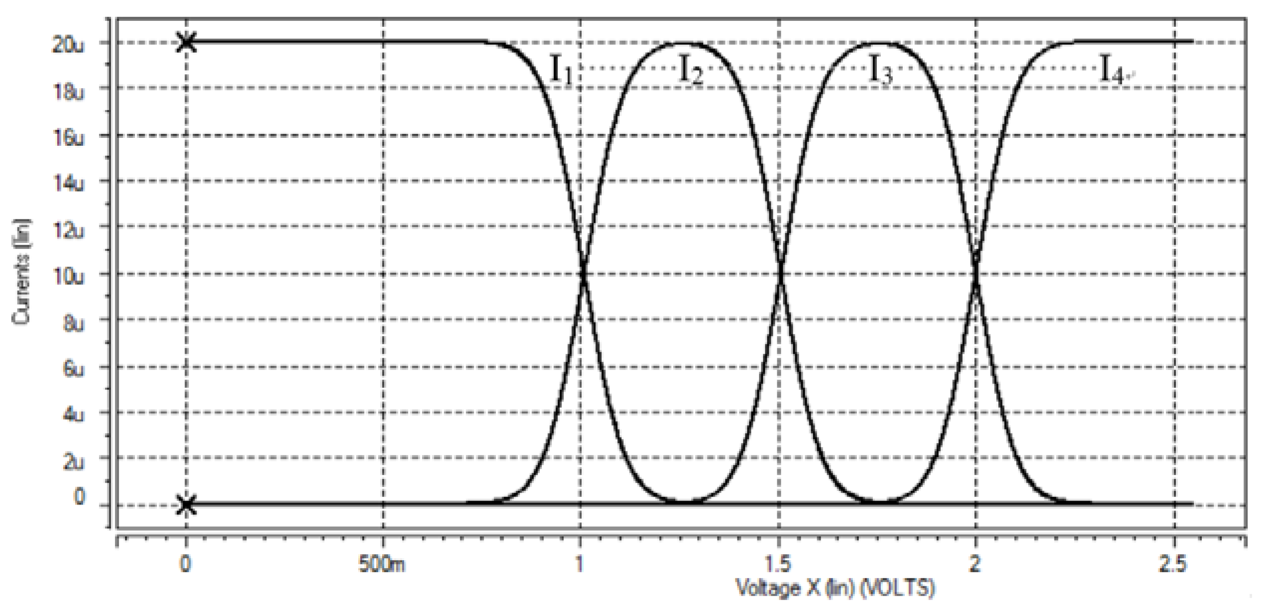
Figure 5.
Proposed Fuzzifier circuit with input crisp voltage of Vin, reference voltages, control switches, and output fuzzy currents of I1 to I4.
Figure 5.
Proposed Fuzzifier circuit with input crisp voltage of Vin, reference voltages, control switches, and output fuzzy currents of I1 to I4.
Figure 6.
Layout of Fuzzifier circuit (of
Figure 5 Left).
Figure 6.
Layout of Fuzzifier circuit (of
Figure 5 Left).
Figure 7.
Layout of proposed Fuzzifier circuit (from
Figure 5).
Figure 7.
Layout of proposed Fuzzifier circuit (from
Figure 5).
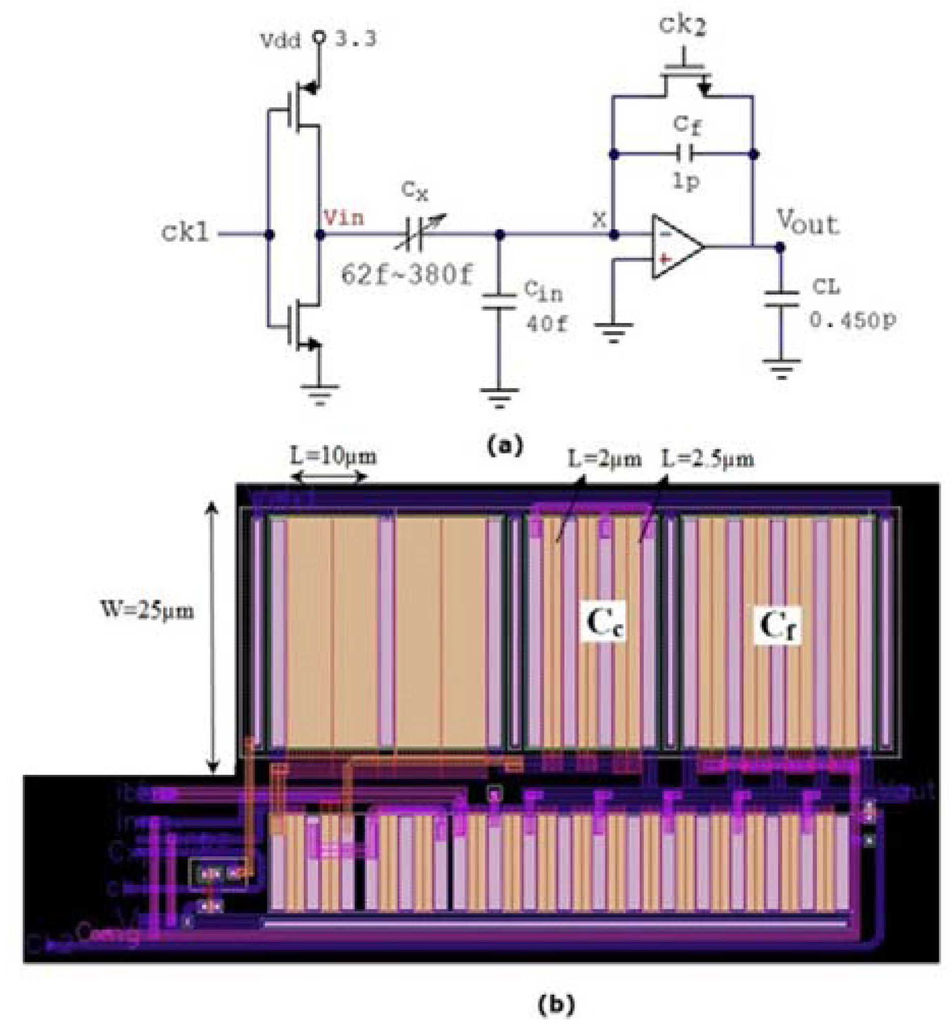
4. Proposed C2V with Application of Fuzzifier Circuit
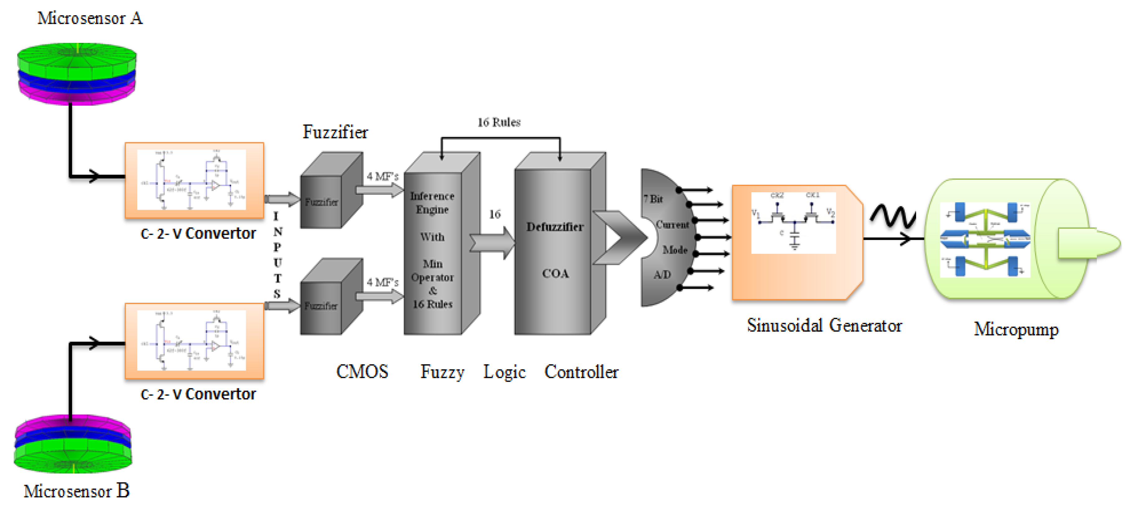
As we know in the Fuzzifier part of the FLC, the Fuzzifier circuit is used to make the antecedents as Fuzzy currents. Hence we used the proposed Fuzzifier circuit here to convert the output signal of sensed blood glucose data to Fuzzy language terms. According to
Figure 12, we previously worked on a MEMS glucose microsensor [
8] which sensed the blood glucose in milli mole to capacitance variations. Thus we proposed a new circuit of capacitance to voltage (C2V) convertor as a bridge between MEMS microsensor and Fuzzifier circuit. The proposed C2V circuit is shown in
Figure 13 with the following details:
- -
Cx is the variable capacitor which is achieved (in range of 62~380 fF) using MEMS glucose microsensor [
8] with taking a sample of blood glucose (of 1~20 mM).
- -
Cin is the parasitic and Op-Amp input transistor (W/L = 10/2) capacitor which is equal to ~40 fF.
- -
Cf is the feedback capacitor with size of transistor
W/
L = 25/10 which is equal ~ 1pF (
Figure 13b).
- -
CL is the load capacitor plus Cgs of next stage transistors (Fuzzifier input).
Figure 12.
Intelligent sensing blood glucose and insulin injection system using MEMS Microsensor, CMOS FLC and MEMS micropump or (Sensing, Fuzzy Processing and Injecting system) [
8].
Figure 12.
Intelligent sensing blood glucose and insulin injection system using MEMS Microsensor, CMOS FLC and MEMS micropump or (Sensing, Fuzzy Processing and Injecting system) [
8].
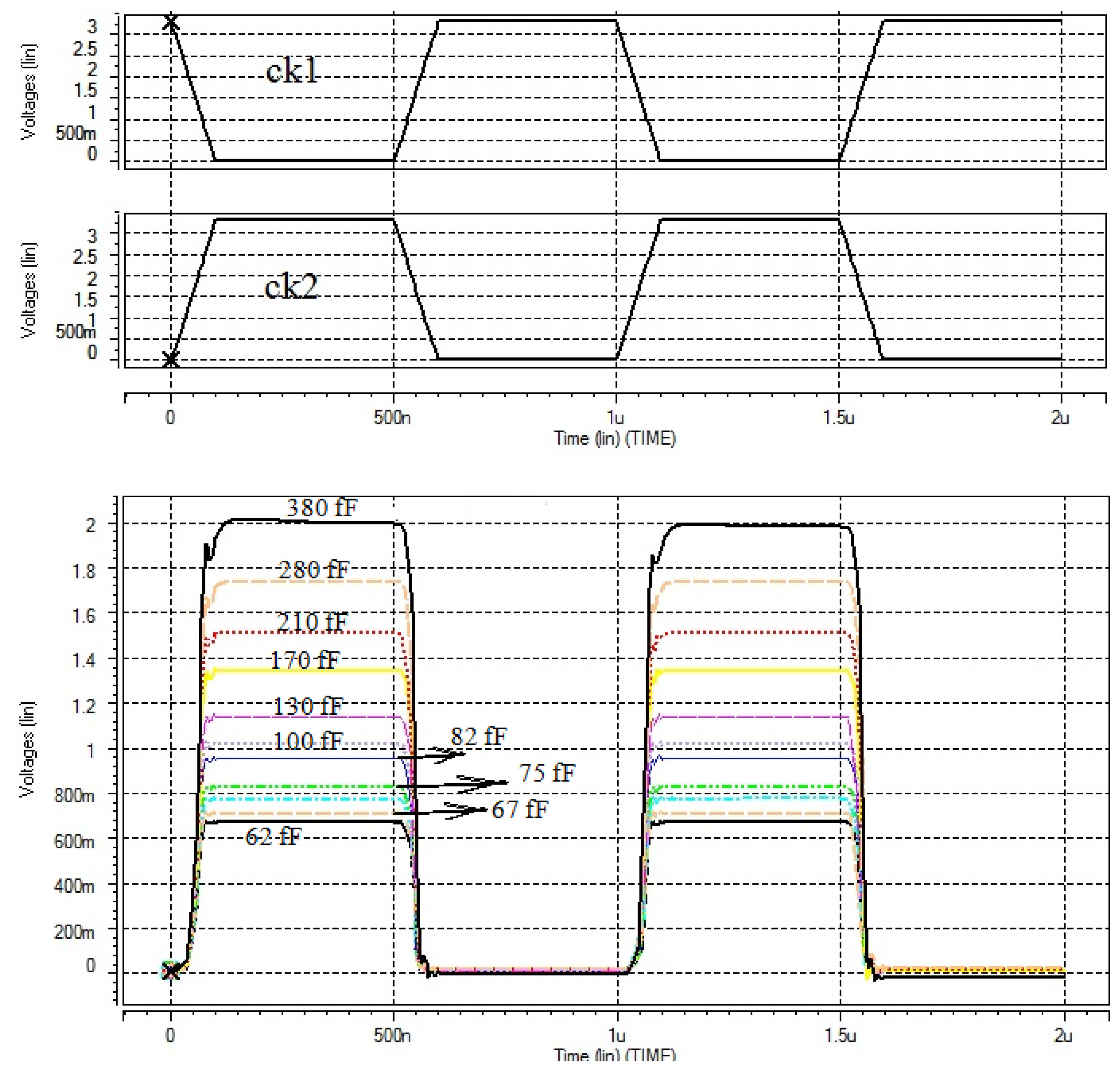
In the circuit of
Figure 13a and using switched capacitor properties, the sampling and amplification mode are achieved using two clocks of ck
1 and ck
2 as follow:
When ck2 is in high level, Cf is discharged via Feedback switch. In this situation, ck1 is in low levels and causes to charge Cx via PMOS transistor of invertor. Thus sampling mode is completed.
Unlike the previous case, when ck
2 and ck
1 are in low and high levels respectively, then the amplification mod is completed. In this situation and writing KCL in node x, the voltage
Vout is achieved by Equations (6) and (7):
On the other hand,
Vout = −
Av/
Vx thus we will have:
It shows that the output voltage of
Vout is a function of
Cx in amplification mode. Thus the minimum op-amp gain which should guarantee gain error of 0.01%, will be obtained according Equation (8):
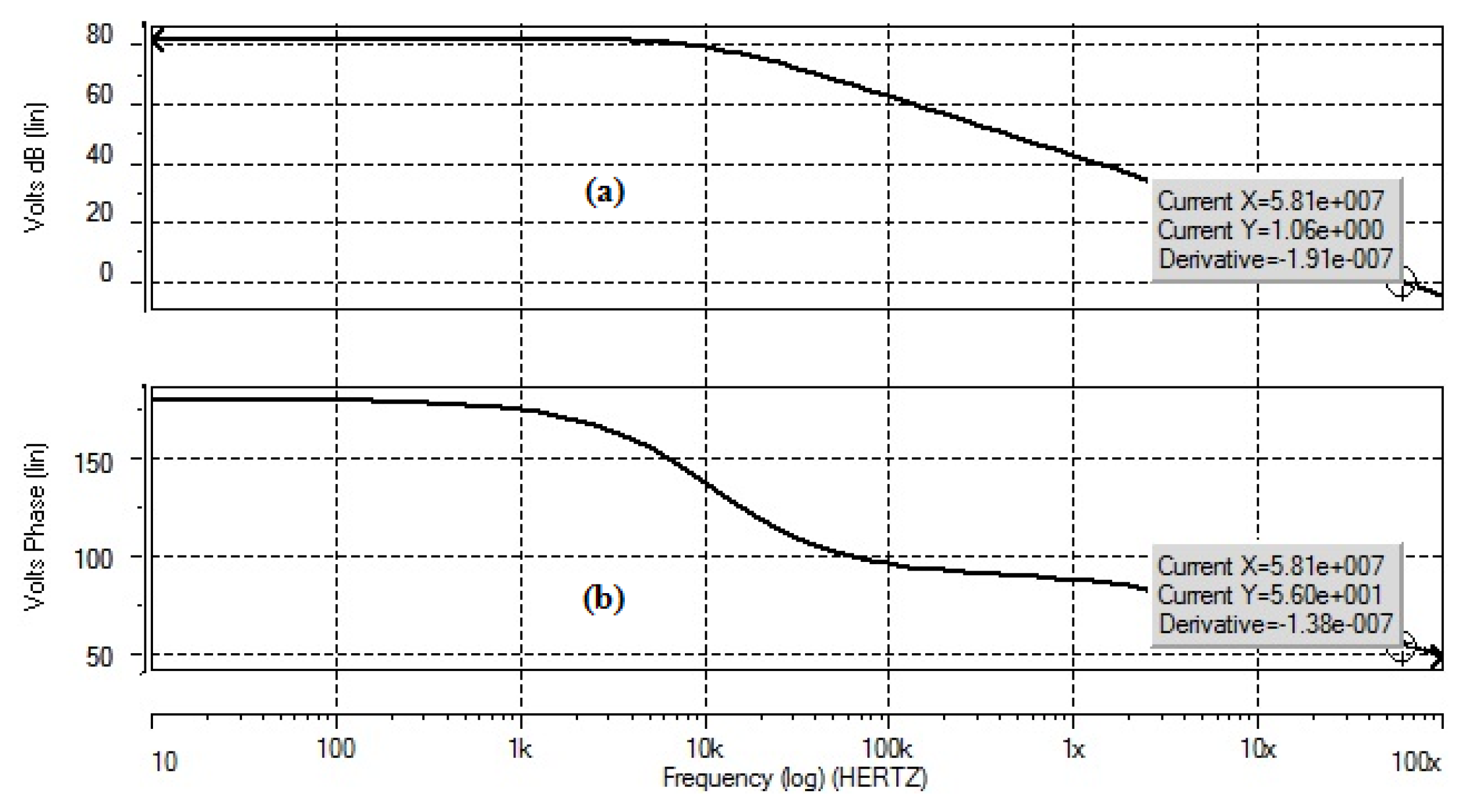
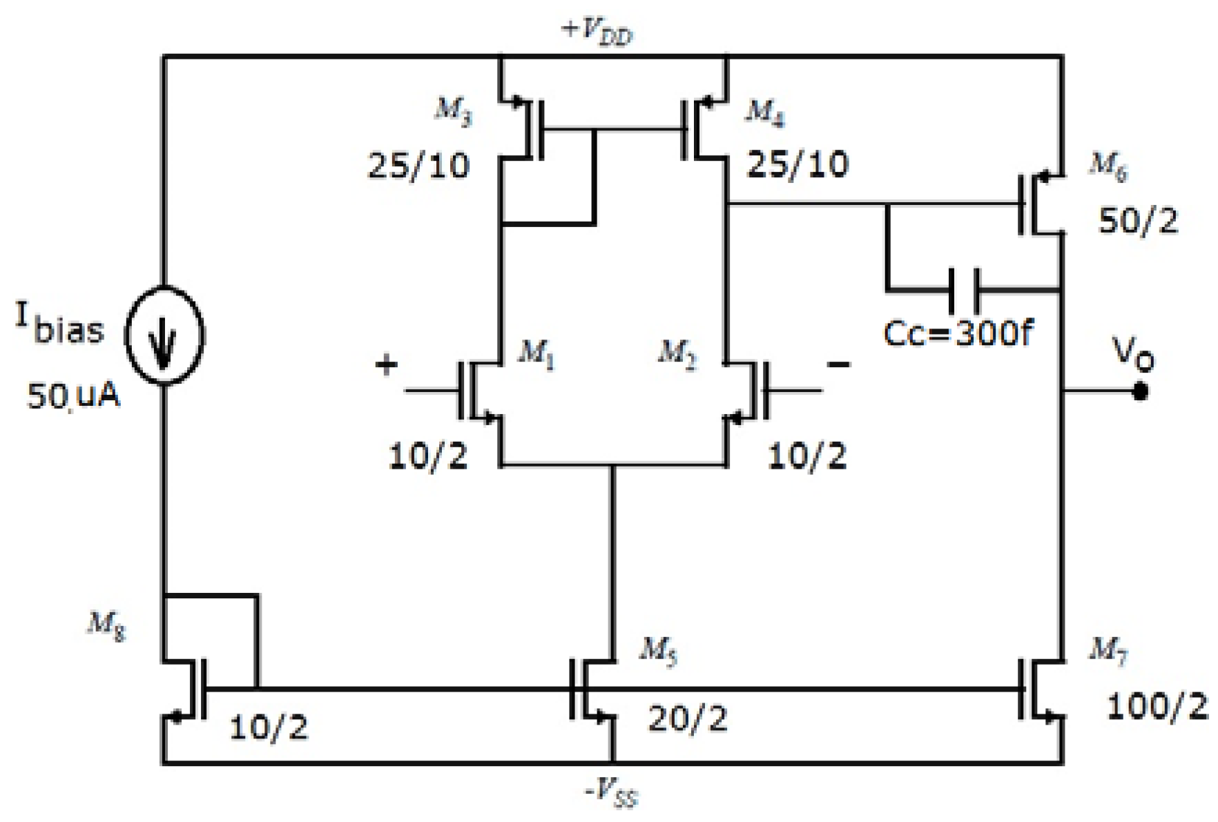
Given the low rate of glucose changes, so according to
Figure 14 we used two-stage op-amp to have high swing and more accuracy. Simulation results of
Figure 15 show the DC gain of ~83 dB and phase margin of 56° which validate Equation (8) and our purpose in the C2V circuit of
Figure 13. Now we apply variable capacitor of
Cx (in range of 62~380 fF) to the proposed C2V circuit. According to
Figure 16 simulation results show that the output voltage of
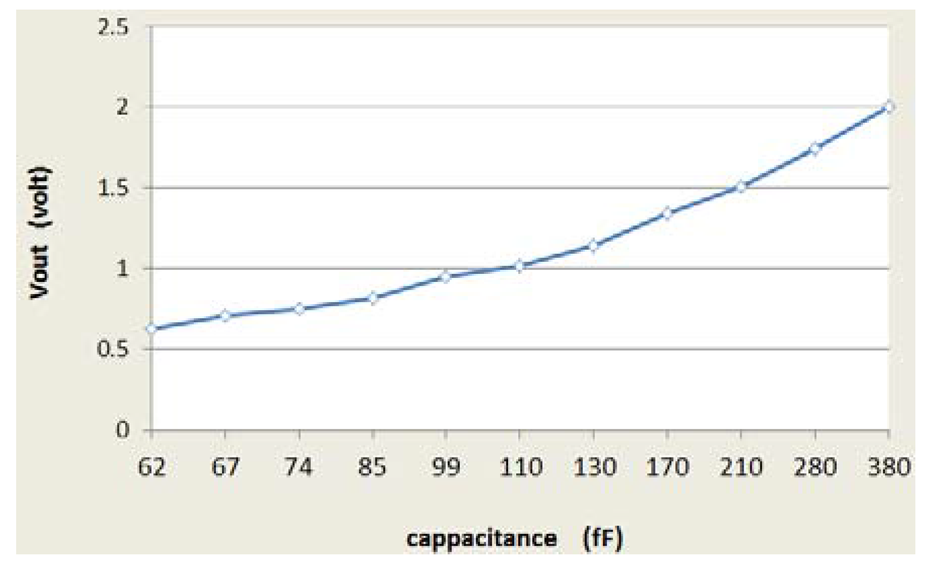
Vout is obtained in range of 0.6~2 V.
Figure 17 shows a suitable linearity of voltage
versus produced capacitance of MEMS glucose microsensor. The proposed C2V circuit is simpler, has a lower die area, and lower power in comparison to previous works [
14,
15].
Figure 13.
Proposed C2V convertor: (a) circuit; (b) Layout.
Figure 13.
Proposed C2V convertor: (a) circuit; (b) Layout.
Figure 14.
Two stage op-amp which designed and used in C2V circuit of
Figure 13.
Figure 14.
Two stage op-amp which designed and used in C2V circuit of
Figure 13.
Figure 15.
Simulation results of two-stage op-amp: (a) DC gain of ~83 dB; (b) phase margin of 56°.
Figure 15.
Simulation results of two-stage op-amp: (a) DC gain of ~83 dB; (b) phase margin of 56°.
Figure 16.
Simulation results of C2V convertor (blood glucose data (capacitance) to voltage of 0.6~2 V).
Figure 16.
Simulation results of C2V convertor (blood glucose data (capacitance) to voltage of 0.6~2 V).
Figure 17.
Obtained voltage versus capacitance of MEMS glucose microsensor.
Figure 17.
Obtained voltage versus capacitance of MEMS glucose microsensor.
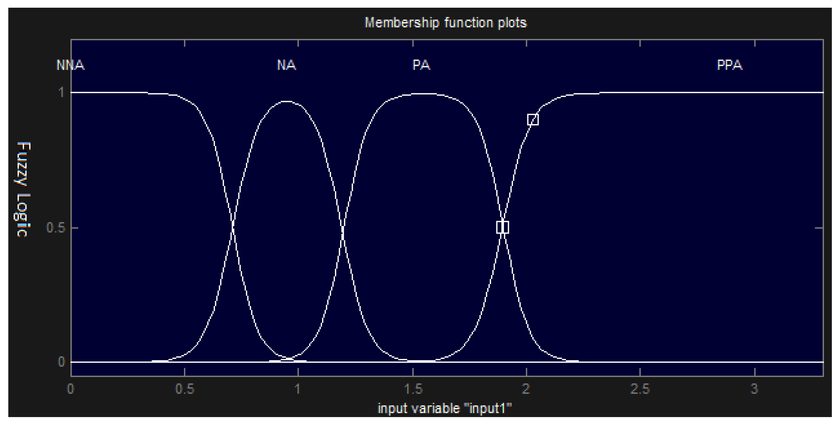
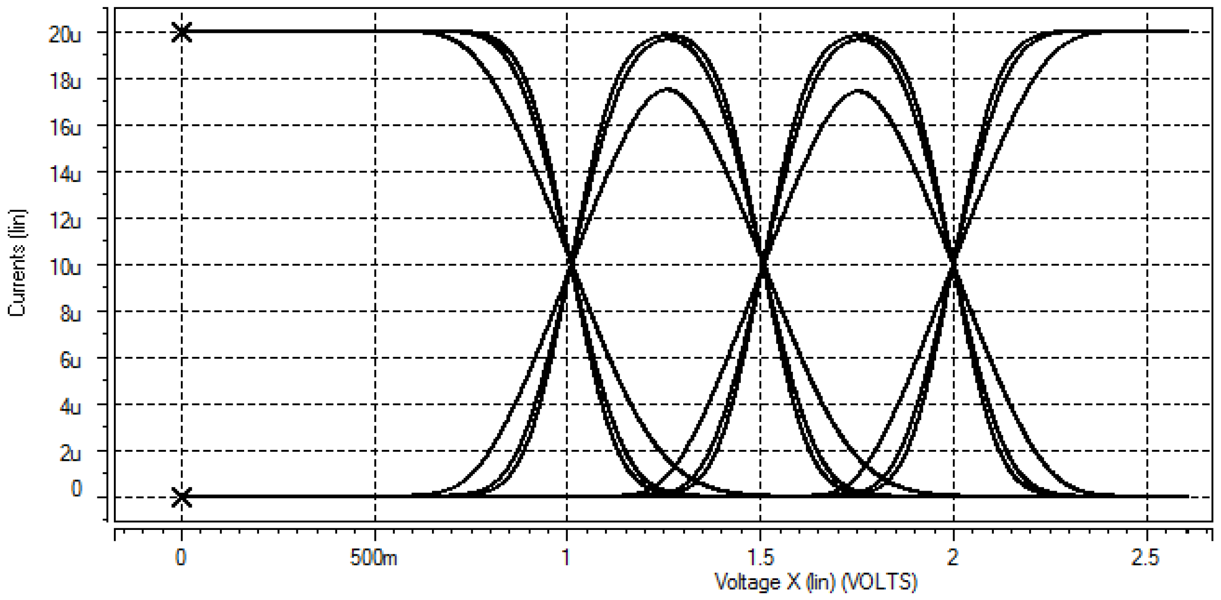
The systematic model of Fuzzifier (from
Figure 12) is evaluated with applying an input which obtained four Fuzzy language terms using Matlab software (
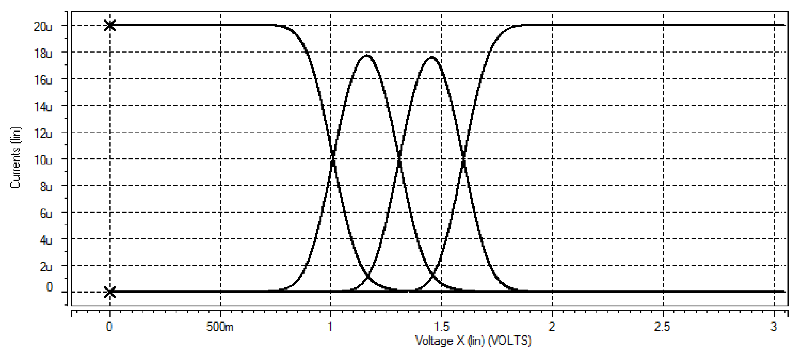
Figure 18). Thus in circuitry, we implemented it with applying output voltage of C2V to the proposed Fuzzifier circuit of
Figure 5, regulating it with digital data, our Fuzzy language terms are obtained using Hspice software (
Figure 19). It shows that there is a good compatibility with the systematic results of
Figure 18.
Figure 18.
Systematic model langue terms of Fuzzifier using MATLAB software.
Figure 18.
Systematic model langue terms of Fuzzifier using MATLAB software.
Figure 19.
Simulation results of obtaining Fuzzy MFs according systematic regulation of
Figure 18 and applying output voltage of C2V (0.6~2 V) to the Fuzzifer circuit (of
Figure 5) using Hspice software.
Figure 19.
Simulation results of obtaining Fuzzy MFs according systematic regulation of
Figure 18 and applying output voltage of C2V (0.6~2 V) to the Fuzzifer circuit (of
Figure 5) using Hspice software.
As mentioned before and according to
Figure 12, the proposed Fuzzifier and C2V circuits can be applicable in designing FLC chip to detect blood glucose, process its data in fuzzy logic environment, and then control micropumps [
16] for Insulin injections.


