Broadband Dual-Phase Plasmons through Metallization of Polymeric Heterojunctions


Institute of Information Photonics Technology and College of Applied Sciences, Beijing University of Technology, Beijing 100124, China
*
Author to whom correspondence should be addressed.
Metals 2017, 7(8), 314; https://doi.org/10.3390/met7080314
Submission received: 1 July 2017
/
Revised: 1 August 2017
/
Accepted: 12 August 2017
/
Published: 16 August 2017
(This article belongs to the Special Issue Metallic Films: From Nanofabrication and Nanostructuration to Characterizations and Applications)
Abstract
:Large-area dual-phase plasmonic gold nanostructures were produced using the phase-separation pattern of a polymer blend film, where two typical light-emitting polymeric semiconductors of poly (9,9-dioctylfluorene-co-benzothiadiazole) (F8BT) and poly (9,9-dioctylfluorene-co-bis-N,N′-(4-butylphenyl)-bis-N,N′-phenyl-1,4 phenylenediamine) (PFB) have been employed to construct the heterojunction patterns. The laser-induced selective cross-linking of F8BT molecules and the subsequent rinsing process using the good solvent of chloroform for PFB supplies a stable template for a further metallization process. When colloidal gold nanoparticles were spin-coated onto the surface of the template, a majority of the gold nanoparticles were confined into the “holes” of originally PFB-rich phase, while a minor portion stays on the “ridges” of F8BT-rich phase. After the annealing process, larger gold nanoparticles were produced inside the holes and smaller ones on the ridges, which induced localized surface plasmon resonance in the near infrared and in the visible, respectively. The structural parameters of the gold plasmonic pattern can be tuned by different surface modification and annealing processes, which can tune the spectroscopic response in the spectral position and in the spectral intensity. The produced nanostructures with broadband plasmon resonance can be used as a template for random lasers with strong optical scattering at both the pump and emission wavelengths and for photovoltaic devices with strong absorption in the visible and near infrared.
1. Introduction
Plasmonic nanostructures with optical response in the infrared [1,2,3,4] are potentially important for exploring efficient photodetectors and for applications in solar cells. Localized surface plasmon resonance or surface plasmon polaritons have been the main physical mechanisms [5]. A series of techniques are available, e.g., electron beam lithography (EBL), for the fabrication of such metallic nanostructures [6,7,8,9], which enables precise control of the shape and size of the produced micro-/nano-structures. However, a small dynamic range of the fabrication area (<200 μm), low speed, and high costs are the obvious disadvantages of this method. The solution-processible fabrication [10,11,12] using colloidal gold nanoparticles has evolved into an important technique for the fabrication of both periodic and randomly distributed nanostructures, which supplies advantages like simplicity, large-area fabrication, and flexible tunability in spectroscopic response of the finished structures. However, this method generally produces structures in nanoscale, which is mainly limited by the size of the structures in the template, the required high concentration of the colloidal solution, and the annealing process of the gold nanoparticles in the size ranging from 5 to 10 nm. Consequently, the resultant plasmon resonance is generally located in the visible spectrum. Thus, it is significant to explore approaches for achieving plasmonic structures resonant in the infrared, making sufficient use of such a solution-processed technique. The corresponding fabrication depends strongly on the patterning on the template substrate.
Laser-induced selective cross-linking in polymer blends [13,14,15] enabled efficient large-area patterning, where the phase-separation scheme may be tuned from nano- to micro-scales. This supplies us an opportunity to template metallic structures with localized surface plasmon resonance in the infrared. In this technique, a blend film of semiconducting polymers of poly (9,9-dioctylfluorene-co-benzothiadiazole) (F8BT) and poly (9,9-dioctylfluorene-co-bis-N,N′-(4-butylphenyl)-bis-N,N′-phenyl-1,4 phenylenediamine) (PFB) is first produced on a glass substrate using spin-coating. The phase-separation scheme between F8BT and PFB can be tuned by changing the composite ratio between these two polymers. The resultant template substrate consists of hole-structures in the size of microns and ridges surrounding the holes, corresponding to PFB-rich and F8BT-rich phases, respectively. Blue-laser illumination induced selective cross-linking of the F8BT molecules, producing a stable template after a rinsing process to remove PFB. Metallization of the template using colloidal gold nanoparticles produced larger plasmonic structures in the holes and smaller ones on the ridge surface, which are resonant in the near infrared and in the visible, respectively. As a result, we achieved a plasmonic substrate with its optical response covering the whole range from 400 nm to 1.7 μm.
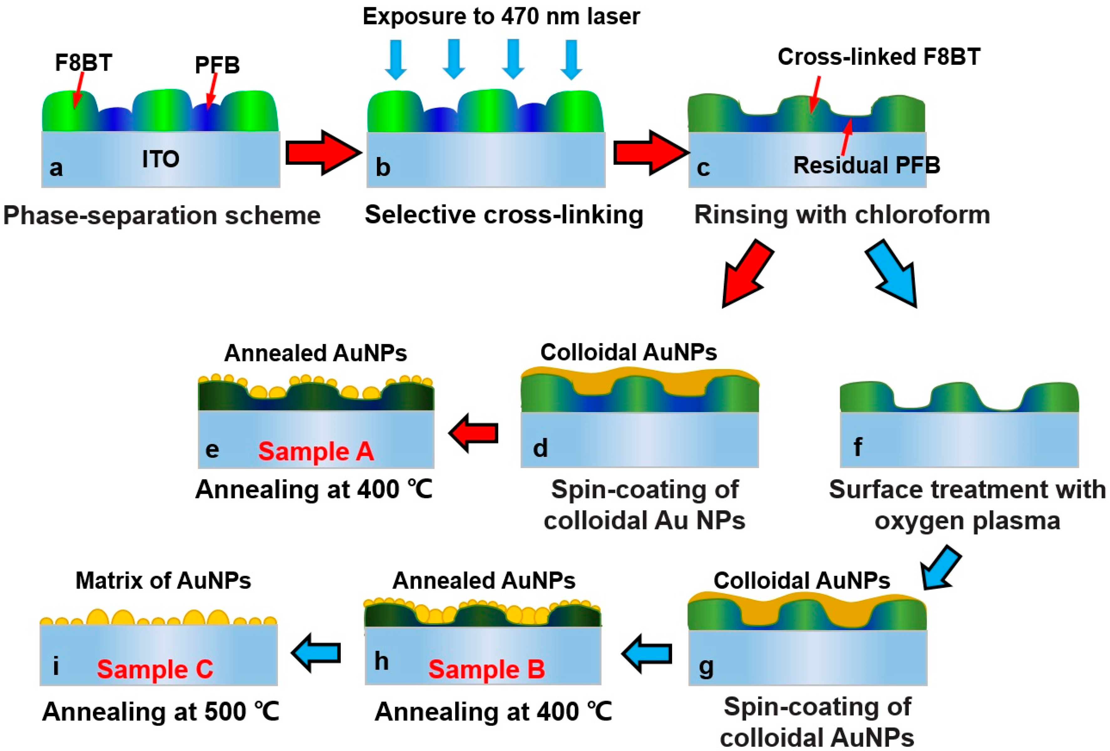
2. Preparation and Stabilization of the Template by Selective Cross-Linking of a Polymeric Phase-Separation Scheme
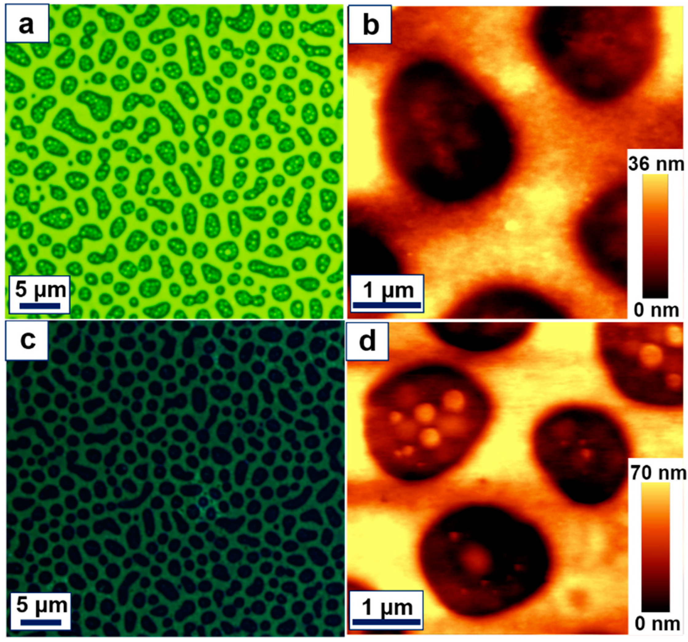
To achieve a large phase-separation scheme, F8BT and PFB were dissolved in chloroform and xylene, respectively, with a concentration of 15 mg/mL before they were mixed with a volume-to-volume ratio of 2:1. Figure 1 presents a summary of the fabrication procedures. The blend solution was then spin-coated onto a fused-silica substrate at a speed of 2000 rpm for 30 s, where the substrate was coated with a layer of 200-nm-thick indium-tin-oxide (ITO), as shown in Figure 1a. The resultant thin film has an average thickness of about 120 nm and the phase-separation between F8BT- and PFB-rich domains can be clearly resolved by the optical microscopic image under UV excitation, as will be shown in Figure 2a. The mechanisms for the phase-separation in F8BT:PFB blend film have been extensively studied and clearly understood [16,17,18]. The green and blue domains correspond to F8BT- and PFB-rich phases, respectively, where the PFB phase is observed as large holes in the blend film and is more than 30 nm lower than the F8BT. The diameter of the PFB phase is larger than 2 μm. However, small particle-like F8BT-rich phases can also be resolved inside the PFB-rich domains, which is more precisely characterized by the atomic force microscopic (AFM) image in Figure 2b.
In the subsequent procedure, the blend film was exposed to a blue laser beam at 470 nm with an average power of about 65 mW and a diameter of about 3 mm for 30 min (Figure 1b). Since F8BT molecules have roughly a peak-absorption at 470 nm, whereas PFB has nearly no absorption of blue light. The exposure using a blue laser beam actually enables selective cross-linking of the F8BT molecules. Thus, rinsing the sample in chloroform removed PFB molecules and left a stable network consisting of F8BT-rich domains (Figure 1c). The polymer film now becomes non-luminescent and insoluble in organic solvent. Furthermore, it becomes thinner and possesses much higher thermal stability [19,20]. Figure 2c,d shows the optical microscope and AFM images of the network of crosslinked F8BT, indicating much larger modulation depth of the phase-separation scheme, which was increased from 36 to 70 nm. In the subsequent procedures, we have two channels to achieve metallization of the samples, where the first channel is demonstrated by Figure 1d,e and the second one by Figure 1f–i. In the first channel, the patterned substrate was obtained immediately after the selective cross-linking process; however, in the second one, the surface of the substrate was treated using an oxygen plasma etching process.
3. Metallization for Achieving Dual-Phase Plasmons
3.1. Direct Annealing of the Spin-Coated Colloidal Gold Nanoparticles on the Phase-Separation Scheme (Sample A)
We have presented the solution-processible fabrication of plasmonic nanostructures using colloidal gold nanoparticles in detail in our previous publications [10,11,21]. Although fabrication of periodical structures was presented in [10,11], the mechanisms for the assembly of gold nanoparticles into the patterned substrate also apply to the random scheme in this work.
The solution-processible metallization processes have employed colloidal gold nanoparticles, which have been synthesized chemically and have a diameter ranging from 5 to 10 nm. In the preparation of the gold nanoparticles, tetraoctylammonium bromide (1.50 g, 2.75 mmol) and hydrogen chloroaurate trihydrate (0.32 g, 0.81 mmol) were dissolved in toluene/water mixture (80 mL/10 mL) with ultrasonicating for 3 min. The aqueous phase was then discarded out of the flask after hydrogen chloroaurate was completely transferred into organic phase. Hexanethiol (0.36 g, 3.04 mmol) was added before 20 mL of freshly prepared aqueous sodium borohydride (0.28 g, 7.4 mmol) solution was rapidly injected into the flask. The aqueous phase was removed again after 4 h of reaction. The remaining organic solvent was removed using a rotary evaporator. The product of the black solid was washed five times with methanol using centrifugal methods and dried with nitrogen completely. Finally, the black powder was dissolved in xylene with a specified concentration, where the gold nanoparticles are covered with ligands of 1-Hexanethiol to ensure excellent dispersity.
In the first channel of metallization process, we spin-coated colloidal gold nanoparticles in xylene with a concentration of 100 mg/mL onto the surface of the above finished template (Figure 1d) before annealing the sample at 400 °C (Figure 1e). The ligands covering the gold nanoparticles were sublimated at a temperature of above 150 °C and the gold nanoparticles have a melting point higher than 200 °C. In the annealing process, the temperature was increased from room temperature to 400 °C with a speed of about 20 °C/min and it was held for about 20 min. Then, the sample was cooled down to room temperature after the furnace was switched off.
It is understandable that the majority of the gold nanoparticles are confined naturally into the “holes” on the template due to the large diameter and modulation depth of the hole-phase sites, forming a thick layer of colloidal gold nanoparticles, as shown in Figure 1d. Additional confinement mechanisms based on the wetting or de-wetting performance are studied in Section 3.5.
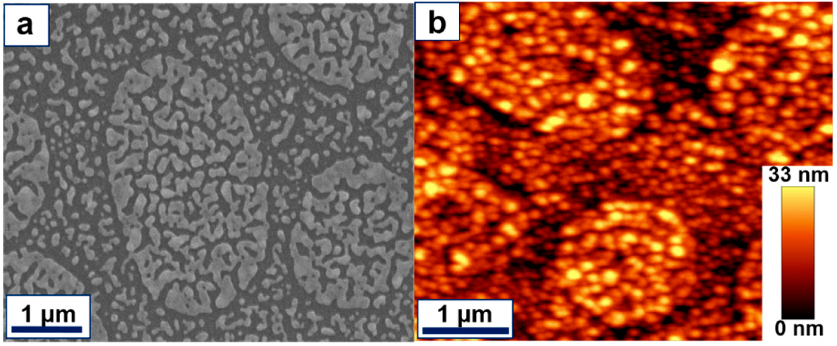
However, a small portion of the gold nanoparticles still stays outside, forming a much thinner layer of the gold nanoparticles, as shown in the optical microscopic image in Figure 3a. During the annealing process, the ligands were evaporated quickly and the gold nanoparticles became molten and aggregated into larger ones. The size of the resultant gold nanoparticles depended strongly on thickness of the gold-particle layer or the amount of the gold nanoparticles per unit area. Therefore, much larger gold nanoparticles were produced inside the “holes” than on the F8BT “ridge” surface, as shown in Figure 1e and in the scanning electron microscopic (SEM) image in Figure 3b. It needs to be noted that the total amount of gold nanoparticles are not sufficient to form a gold “disk” or “plate” inside the holes; instead, we observed large particles that are distributed randomly on the hole sites. These large gold nanoparticles are basically irregular according to the SEM image in Figure 3b, which have an average size of up to 135 nm, according to statistical evaluations. The smaller ones remaining on the F8BT surface have an average diameter smaller than 50 nm. Figure 3c shows the atomic force microscopic image of the dual-phase gold nanoparticles and Figure 3d shows the plot of the profile of the height image in Figure 3c; both show a modulation depth as large as 25 nm inside the holes and smaller than 10 nm on the ridge surfaces. Actually, it is a more suitable characterization to evaluate the occupation ratio by gold inside and outside the holes or on the F8BT ridge surface. We measured an occupation ratio of 48% and 33% by gold inside and outside the holes, respectively, using the SEM image in Figure 3b.
3.2. Annealing after Surface Modification Using Oxygen-Plasma Etching (Sample B)
We can tune the shape, size, and distribution of the plasmonic nanostructures by modifying the surface properties of the polymer template. This can be achieved by a thin-layer etching into the polymer blend film using oxygen plasma. The corresponding procedures are defined in the second channel demonstrated in Figure 1f–i. We used the same batch of templates for the fabrication of Sample A in the oxygen plasma etching. A plasma cleaner (PDC-32G) system was employed and a power of 6.8 W was used to perform the etching process for 12 min. Then, we spin-coated the colloidal solution onto the surface-treated blend film, as shown in Figure 1g, before we annealed the sample at 400 °C for 20 min to produce the Sample B (Figure 1h). Figure 3e shows the optical microscopic images of the sample immediately after the spin-coating process and Figure 3f shows the SEM image of the fabricated dual-phase plasmonic structures after the annealing process. Figure 3g,h shows the AFM height image and a profile plot, respectively. According to Figure 3f–h, the gold nanostructures become larger and more irregular inside and outside the hole phases, implying that more colloidal gold nanoparticles have been coated on the surface of the template due to the modification processes. It is now difficult to evaluate the size of the gold structures. In particular, the gold tends to become connected to form a continuous disk and the gold occupation ratio was increased to larger than 62% inside the holes and reduced to smaller than 27% outside the hole. Thus, the surface modification process using oxygen plasma etching enable more confinement of gold into the holes.
Furthermore, we can also observe from Figure 3g,h that the modulation depth became larger over the whole structures. The average modulation depth is as large as 30 nm inside the holes and smaller than 15 nm outside the holes. This implies much larger surface roughness of Sample B, which resulted from the surface modification process through oxygen plasma etching.
3.3. Removal of the Polymeric Template through Further Annealing at 500 °C (Sample C)
Considering possible requirements in practical applications, we still need to remove the remaining polymer of F8BT. Then, we annealed the Sample B produced in the early stages of the second channel further to higher than 500 °C to produce Sample C, so that the polymer molecules were evaporated completely, as illustrated in Figure 1i. This higher-temperature annealing process has also modified the plasmonic structures. Figure 4a,b shows the SEM and AFM images of the Sample C, which was produced by annealing Sample B at 500 °C for 20 min. The annealing process at 500 °C has reduced both the height and the size of the gold nanostructures and reduced the contrast between the two phases. In particular, the previous phase consisting of larger gold nanoparticles in the PFB-hole-structures becomes higher than that of small gold nanoparticles on the surface of F8BT-phase due to the removal of the F8BT template.
All of the gold nanoparticles in different phases are now sitting on the ITO-glass substrate and they have again experienced a melting-solidification process. This led to some further changes in the height and shape of the gold nanostructures, resulting changes in the plasmonic resonance spectrum, as will be investigated in Section 4.
3.4. Tuning the Microscopic Performance by Changing the Preparation Conditions
There exists an optimized set of fabrication parameters, which can be obtained by tuning the plasmonic nanostructures with changing the fabrication conditions. Figure 5 shows the SEM images of the fabrication results with changing the concentration of the colloidal solutions and the annealing temperatures. For the SEM data in Figure 5a–c, the annealing temperature has been fixed at 400 °C and the concentration of the cooloidal solution was increased from 60 to 120 mg/mL. At a low concentration of 60 mg/mL, the amount of gold nanoparticles are not large enough to produce large gold nanoparticles (AuNPs) with high density. However, at a concentration as high as 120 mg/mL, the large amount of AuNPs and the much increased viscocity of the colloidal solution may reduce the confinement mechanisms. As a result, a large amount of AuNPs were produced outside the hole phases with much increased sizes. Comparing Figure 5a–c, we may find that the concentration of 100 mg/mL is close to the optimization.
Figure 5d–f shows the fabrication results at a concentration of 100 mg/mL for the colloidal solution and an annealing temperature of 200, 400, and 500 °C, respectively. At an annealing temperature of 200 °C, the colloidal gold nanoparticles were not molten and interacted sufficiently, so that AuNPs with clearly defined borders and sizes were not obtained. Using an annealing temperature of 400 °C, we can achieve excellent confinement of the AuNPs into the holes that were originally the PFB-rich phases. Dual-phase plasmonic structures can be obtained with clearly defined borders and clearly different sizes inside and outside the “holes”. When the annealing temperature was increased to 500 °C, as the polymeric template was removed, the AuNPs become more irregular, the borders between the two plasmonic phases become less clear, and the size difference between the AuNPs was also reduced. Therefore, for the dual-phase plasmonic structures, 400 °C may be taken as an optimized annealing temperature. It should be noted that all of the samples in Figure 5 have experienced an oxygen plasma treatment process before the metalization process.
3.5. The Role of Wetting Performance in the Responsible Mechanisms
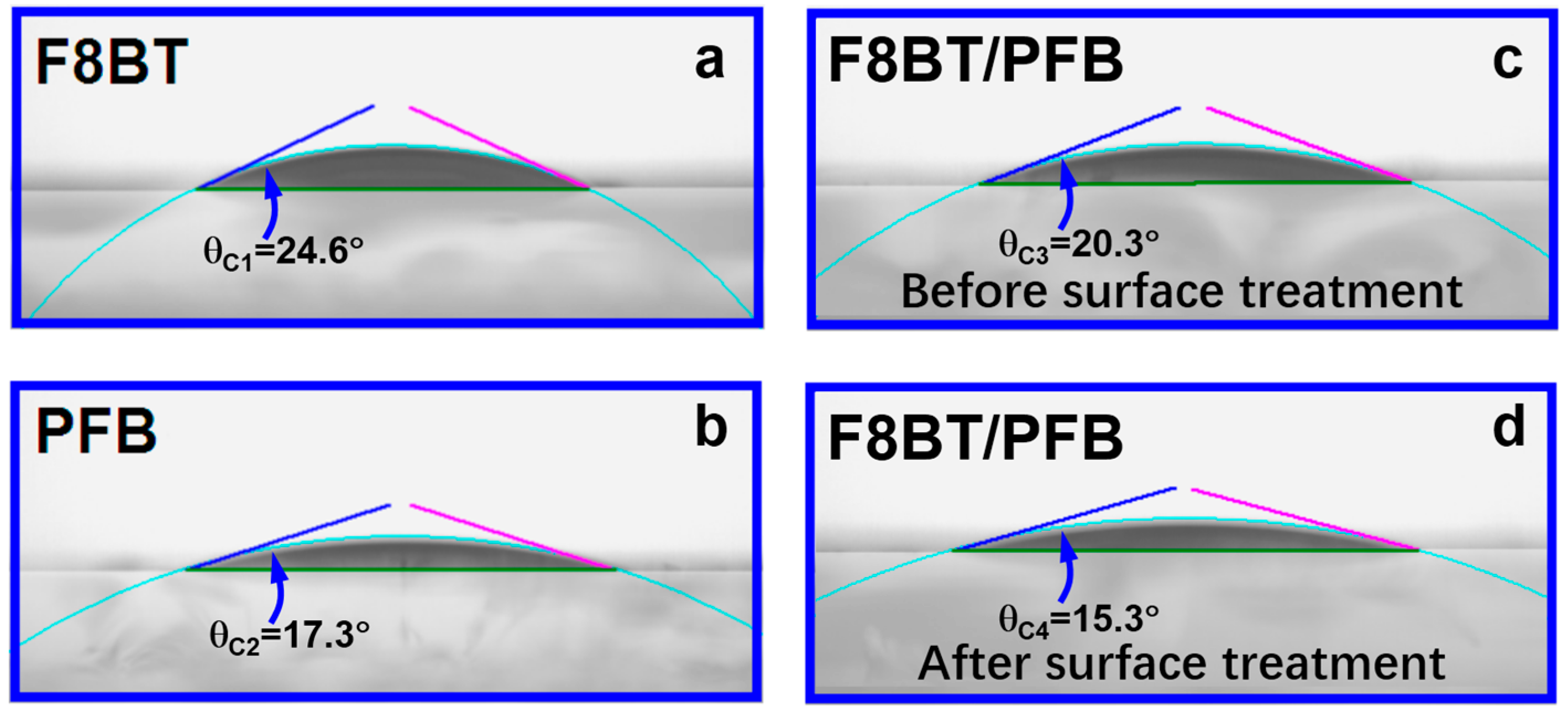
We need to consider wetting and de-wetting performances for understanding the mechanisms in the fabrication process. The wetting performance of the colloidal solution of gold nanoparticles has played the main role in determining the confinement of AuNPs into the hole phases in the patterned substrate. Therefore, we present in Figure 6 the measurements of contacting angles of the colloidal solution on the surfaces of thin films of F8BT, PFB, F8BT:PFB blend without treatment by oxygen plasma, F8BT:PFB blend after being treated by oxygen plasma in Figure 6a–d, respectively. Clearly, the colloidal solution wets PFB better than F8BT and wets the oxygen-plasma-treated blend film better than the non-treated, explaining well why the majority of the gold nanoparticles were confined into the holes bottomed with the remaining PFB.
Furthermore, the thermal de-wetting of the molten gold on the polymer-patterned substrate has also played important roles in determining the morphology of the final plasmonic nanostructures, although such effect did not influence much the confinement process. This mechanism took effect during the annealing processes and determined the size and shape of the AuNPs on local sites. The related investigations have been reported in our previous work [21] and in literature [22,23].
4. Optical Spectroscopic Performance
Figure 7 shows the optical extinction spectra of the metalized Samples A (solid red), B (solid black), and C (dashed black), corresponding to those demonstrated in Figure 3 and Figure 4, respectively. The optical extinction spectrum has been calculated using log10[Is(λ)/I0(λ)], where I0(λ) and Is(λ) are the incident and transmitted spectra through the structures. Thus, optical density (OD) can be used as units for the amplitude values of the optical extinction spectra. For Sample A, we observe two plasmon features peaked at about 620 and 1050 nm with an amplitude of 0.64 and 0.68 OD, respectively. These two peaks correspond to the gold nanoparticles on the original locations of the F8BT- and PFB-rich phases, respectively, in the template, as indicated in the inset SEM image. These two features are indicated by the two arrows in Figure 7, relating the SEM image to the optical extinction spectra. The two peaks have nearly equal amplitudes.
Due to the difference in the annealing process and in the oxygen-plasma etching process, the resonance spectra of the two plasmons of Sample B shifted slightly to the red, which are peaked at 650 and 1070 nm with an amplitude of 0.76 and 0.96 OD, respectively. Meanwhile, the two resonance spectra become broadened and enhanced. These phenomena indicate that the gold nanoparticles became larger and less homogeneous in Sample B than in A. However, the peak at 1070 nm has obviously larger amplitude than that at 650 nm, implying stronger plasmons in the near infrared for the gold nanoparticles located in the PFB hole-phase in the original blend film. It should be noted that the spectral peaks at about 400 nm for all of the spectra in Figure 7 have actually resulted from the intrinsic higher optical transmission or lower extinction at about 500 nm of gold.
After a further annealing process at 500 °C, the spectrum of plasmon resonance of Sample C becomes significantly enhanced at the shorter-wavelength peak around 645 nm with an amplitude of 0.93 OD, whereas the spectral intensity becomes reduced at the longer-wavelength one around 1090 nm with an amplitude of 0.87 OD, as compared with Sample B. Meanwhile, the shorter-wavelength peak becomes narrower in spectral bandwidth and the longer-wavelength one becomes broader.
In our previous works on the randomly distributed gold nanoparticles fabricated using colloidal gold nanoparticles [21,24] and in the reported structures [23], the peak values of optical extinction have been generally smaller than 0.6 OD. However, in this work, the optical extinction ranges from larger than 0.6 OD to larger than 0.9 OD, as shown in Figure 7, implying much enhanced efficiency of optical extinction.
Thus, we have achieved broadband optical extinction spectra, making use of the dual-phase localized surface plasmon resonance (LSPR) of gold nanoparticles at different locations, which extend from about 500 to 1600 nm with efficient optical absorption and scattering. We have the following mechanisms to explain the spectroscopic response of the dual-phase gold nanostructures: (1) the size-dependence of the plasmonic nanostructures, which is determined by the height (H), the diameter (D), and the value of H/D. A larger value of H/D corresponds to a blue-shift of plasmon resonance of gold nanoparticles [25,26]. Gold nanoparticles on the F8BT- and PFB-rich phases have larger differences in H, D, and H/D, resulting in LSPR in the visible and in the infrared, respectively; (2) the environmental dielectric constants (ε). A larger value of ε leads to a red-shift of plasmon resonance of gold nanoparticles. Different contacts of gold nanoparticles with the substrate within the F8BT- and PFB-phase regions have influenced the LSPR spectrum differently. This explains why different annealing processes have influenced LSPR of the gold-nanoparticle samples differently; (3) the shape of the gold nanostructures. Larger gold nanostructures with more irregular shapes led to red-shift and broadening of the resonance spectrum. Moreover, high irregularity in the gold nanoparticles induced different responses for different polarizations of light, leading to further broadening of the LSPR spectrum.
5. Dark-Field Characterization
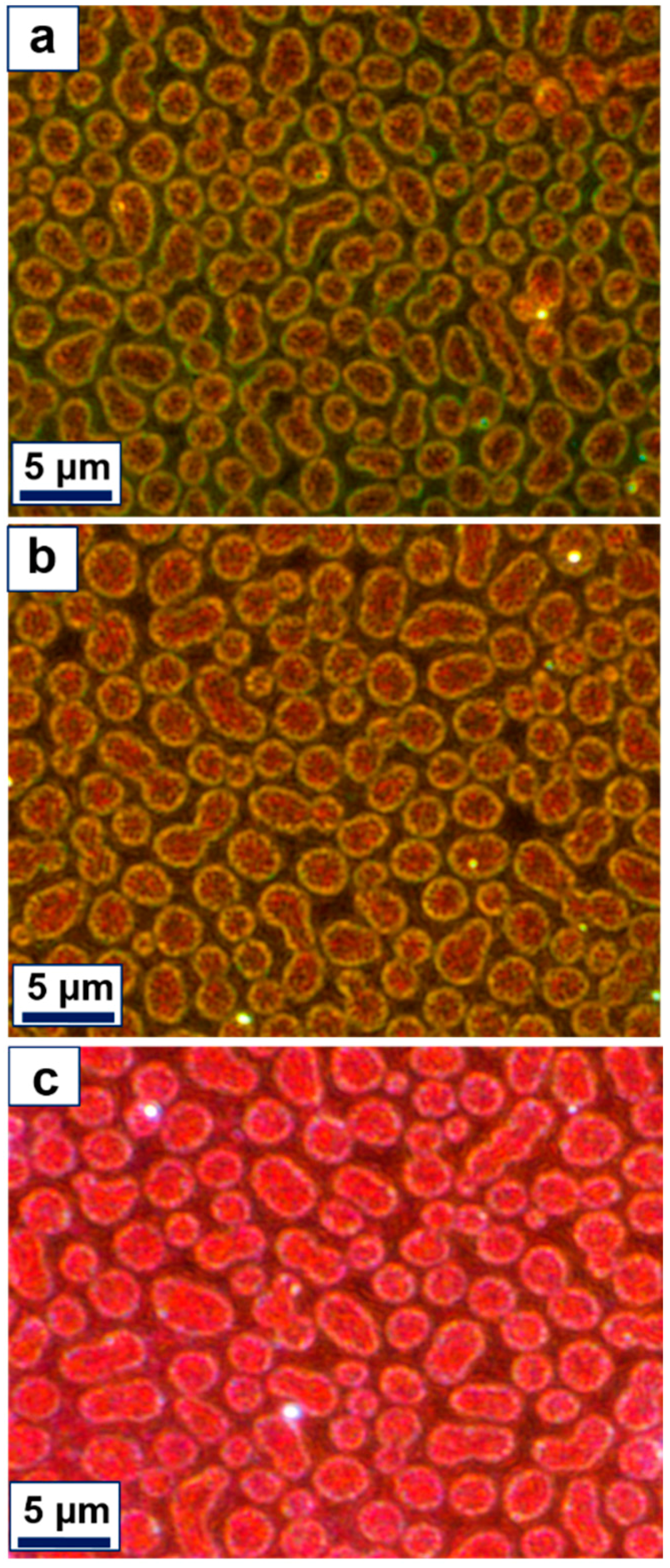
Figure 8a–c shows the dark-field optical microscopic images of Samples A–C, respectively. A Nikon eclipse LV 100 ND microscope (Tokyo, Japan) equipped with a 50 W halogen lamp and a 100× objective lens was used in the dark-field image acquisition. The colors of the scattered light resolve differently resonant plasmons. The sizes and shapes of the nanostructures have significantly influenced the scattered light color and intensity. Therefore, the structures in the holes, on the ridge surfaces, and on the borders are observed in different colors in the dark field.
For Samples A and B, there exists a transition border from the F8BT ridges to the PFB holes, which has an intermediate dielectric constant between F8BT and ITO. Thus, we observed a yellow border on each of the red “grains”. Larger gold nanoparticles are located inside the holes, corresponding to the plasmon resonance in the red and in the infrared. Smaller ones are coating the ridges and partially embedded in the F8BT film, corresponding to plasmon resonance mainly in the green, partially in the yellow and red. This is clearly observed in Figure 8a. However, for Sample B shown in Figure 8b, the green color becomes weak because much larger gold nanoparticles were produced on the ridge surface than for Sample A. Meanwhile, the red and yellow colors become brighter, which agrees with the microscopic images in Figure 3 and the spectroscopic images in Figure 7.
For Sample C, both the smaller and larger gold nanoparticles are now sitting on the ITO glass, and the dielectric constant were increased dramatically for the smaller ones, leading to redshift of plasmon resonance. As a result, light scattering in the red can be observed over the whole structure, as shown in Figure 8c, although a border is still observable for each grain. Now the border scattering results mainly from the intrinsic gold reflection at the surface of the large particles.
Furthermore, there exists a gap between the grain and ridge, corresponding to the original heterojunction in the template. Light scattering may be more efficiently coupled out at the borders than inside the holes, where localization of light by the multifold reflection and scattering between the gold nanoparticles was reduced.
6. Conclusions
We demonstrated fabrication of large-area gold micro-grains using a template of the phase-separation scheme of the F8BT:PFB polymer blends. The phase-separation pattern enabled dual-phase fabrication of plasmonic gold nanostructures. Laser-induced cross-linking not only enabled “solidification” or “stabilization” process, but also modified the surface properties of the template. Oxygen-plasma-etching and high-temperature annealing has tuned the microscopic and spectroscopic performances of the plasmonic structures further. Plasmon resonance of the resultant micro-/nano-hybrid structures covers the whole visible band and extends to the infrared, showing two peaks around 600 and 1100 nm and a broad extinction spectrum ranging from 400 nm to 1.7 μm. These unique features are important for the exploring optoelectronic devices operating in the infrared. In particular, the dual-phase performance is important for plasmonic lasers, where the shorter- and longer-wavelength resonance modes supply optical feedback for the pump and emitting lasers, respectively.
Acknowledgments
We acknowledge the National Natural Science Foundation of China (11574015, 11434016) for the support.
Author Contributions
Cuiying Huang performed the experiments, measured all of the data presented in the manuscript, did some of the data processing and wrote a draft of the paper. Xinping Zhang designed this research work, supervised the experimental work, did the data analysis, and wrote this paper.
Conflicts of Interest
The authors declare no conflict of interest.
References
- Yu, Y.Y.; Chang, S.S.; Lee, C.L.; Wang, C.R.C. Gold nanorods: Electrochemical synthesis and optical properties. J. Phys. Chem. B 1997, 101, 6661–6664. [Google Scholar] [CrossRef]
- Munoz-Noval, A.; Fukami, K.; Martin-Palma, R.J.; Sakka, T.; Manso-Silvan, M.; Ogata, Y.H. Surface plasmon resonance study of Au nanorod structures templated in mesoporous silicon. Plasmonics 2013, 8, 35–40. [Google Scholar] [CrossRef]
- Deng, B.C.; Guo, Q.S.; Li, C.; Wang, H.Z.; Ling, X.; Farmer, D.B.; Han, S.J.; Kong, J.; Xia, F.N. Coupling-enhanced broadband mid-infrared light absorption in graphene plasmonic nanostructures. ACS Nano 2016, 10, 11172–11178. [Google Scholar] [CrossRef] [PubMed]
- Ueno, K.; Sun, Q.; Mino, M.; Itoh, T.; Oshikiri, T.; Misawa, H. Surface plasmon optical antennae in the infrared region with high resonant efficiency and frequency selectivity. Opt. Express 2016, 24, 17728–17737. [Google Scholar] [CrossRef] [PubMed]
- Zayatsa, A.V.; Smolyaninovb, I.I.; Maradudinc, A.A. Nano-optics of surface plasmon polaritons. Phys. Rep. 2005, 408, 131–314. [Google Scholar] [CrossRef]
- Alegret, J.; Rindzevicius, T.; Pakizeh, T.; Alaverdyan, Y.; Gunnarsson, L.; Kall, M. Plasmonic properties of silver trimers with trigonal symmetry fabricated by electron-beam lithography. J. Phys. Chem. C 2008, 112, 14313–14317. [Google Scholar] [CrossRef]
- Lin, V.K.; Teo, S.L.; Marty, R.; Arbouet, A.; Girard, C.; Alarcon-Llado, E.; Liu, S.H.; Han, M.Y.; Tripathy, S.; Mlayah, A. Dual wavelength sensing based on interacting gold nanodisk trimers. Nanotechnology 2010, 21, 305501. [Google Scholar] [CrossRef] [PubMed]
- Liu, Y.J.; Leong, E.S.P.; Wang, B.; Teng, J.H. Optical transmission enhancement and tuning by overylaying liquid crystals on a gold film with patterned nanoholes. Plasmonics 2011, 6, 659–664. [Google Scholar] [CrossRef]
- Wang, L.; Nishijima, Y.; Ueno, K.; Misawa, H.; Tamai, N. Plasmon coupling and coherent acoustic phonon dynamics of periodic gold pair nanocuboids by near-IR transient absorption spectroscopy. J. Photochchem. Photobiol. A 2011, 221, 164–168. [Google Scholar] [CrossRef]
- Zhang, X.P.; Sun, B.Q.; Friend, R.H.; Guo, H.C.; Nau, D.; Giessen, H. Metallic photonic crystals based on solution-processible gold nanoparticles. Nano Lett. 2006, 6, 651–655. [Google Scholar] [CrossRef] [PubMed]
- Zhang, X.P.; Sun, B.Q.; Guo, H.C.; Tetreault, N.; Giessen, H.; Friend, R.H. Large-area two-dimensional photonic crystals of metallic nanocylinders based on colloidal gold nanoparticles. Appl. Phys. Lett. 2007, 90, 133114. [Google Scholar] [CrossRef]
- Liu, H.M.; Zhang, X.P.; Zhai, T.R. Plasmonic nano-ring arrays through patterning gold nanoparticles into interferograms. Opt. Express 2013, 21, 15314–15322. [Google Scholar] [CrossRef] [PubMed]
- Berta, M.; Biver, E.; Maria, S.; Phan, T.N.T.; D’Aleo, A.; Delaporte, P.; Fages, F.; Gigmes, D. Nanosecond laser-induced periodic surface structuring of cross-linked azo-polymer films. Appl. Surf. Sci. 2013, 282, 880–886. [Google Scholar] [CrossRef]
- Zhang, X.P.; Li, H.W. Laser-induced selective crosslinking for scaling the heterointerfacial domain in polymer blends. Opt. Express 2013, 21, 24620–24629. [Google Scholar] [CrossRef] [PubMed]
- Zhang, X.P.; Liu, F.F.; Li, H.W. Selective photophysical modification on light-emitting polymer films for micro- and nano-patterning. Materials 2016, 9, 121. [Google Scholar] [CrossRef] [PubMed]
- Morteani, A.C.; Sreearunothai, P.; Herz, L.M.; Friend, R.H.; Silva, C. Exciton regeneration at polymeric semiconductor heterojunctions. Phys. Rev. Lett. 2004, 92, 247402. [Google Scholar] [CrossRef] [PubMed]
- Charas, A.; Alves, H.; Alcacer, L.; Morgado, J. Use of cross-linkable polyfluorene in the fabrication of multilayer polyfluorene-based light-emitting diodes with improved efficiency. Appl. Phys. Lett. 2006, 89, 143519. [Google Scholar] [CrossRef]
- Abdulla, M.; Renero-Lecuna, C.; Kim, J.S.; Friend, R.H. Morphological study of F8BT:PFB thin film blends. Org. Electron. 2015, 23, 87–98. [Google Scholar] [CrossRef]
- Inaoka, S.; Roitman, D.B.; Advincula, R.C. Cross-linked polyfluorene polymer precursors: Electrodeposition, PLED device characterization, and two-site co-deposition with poly(vinylcarbazole). Chem. Mater. 2005, 17, 6781–6789. [Google Scholar] [CrossRef]
- Zhang, X.P.; Liu, H.M.; Li, H.W.; Zhai, T.R. Direct nanopatterning into conjugated polymers using interference crosslinking. Macromol. Chem. Phys. 2012, 213, 1285–1290. [Google Scholar] [CrossRef]
- Zhang, X.P.; Liu, H.M.; Feng, S.F. Solution-processible fabrication of large-area patterned and unpatterned gold nanostructures. Nanotechnology 2009, 20, 425303. [Google Scholar] [CrossRef] [PubMed]
- Alexander, B.T.; Chuntonov, L.; Karakouz, T.; Bendikov, T.A.; Haran, G.; Vaskevich, A.; Rubinstein, I. Tunable localized plasmon transducers prepared by thermal dewetting of percolated evaporated gold films. J. Phys. Chem. C 2011, 115, 24642–24652. [Google Scholar]
- Sun, H.; Yu, M.; Wang, G.; Sun, X.; Lian, J. Temperature-dependent morphology evolution and surface plasmon absorption of ultrathin gold island films. J. Phys. Chem. C 2012, 116, 9000–9008. [Google Scholar] [CrossRef]
- Zhang, X.P.; Li, H.W.; Wang, Y.M.; Liu, F.F. Stimulated emission within the exciplex band by plasmonic-nanostructured polymeric heterojunctions. Nanoscale 2015, 7, 5624–5632. [Google Scholar] [CrossRef] [PubMed]
- Kooij, E.S.; Ahmed, W.; Zandvliet, H.J.W.; Poelsema, B. Localized plasmons in noble metal nanospheroids. J. Phys. Chem. C 2011, 115, 10321–10332. [Google Scholar] [CrossRef]
- Zhang, S.; Li, G.C.; Chen, Y.Q.; Zhu, X.P.; Liu, S.D.; Lei, D.Y.; Duan, H.G. Pronounced fano resonance in single gold split nanodisks with 15 nm split gaps for intensive second harmonic generation. ACS Nano 2016, 10, 11105–11114. [Google Scholar] [CrossRef] [PubMed]
Figure 1.
Fabrication procedures: (a) spin-coating of the blend film to form the phase-separation scheme; (b) exposure of the blend film to the 470-nm laser beam to achieve selective cross-linking of the F8BT molecules; (c) rinsing using chloroform; (d) spin-coating of colloidal gold nanoparticles; (e) annealing at 400 °C to produce Sample A; (f) surface treatment using oxygen plasma; (g) spin-coating of colloidal gold nanoparticles; (h) annealing at 400 °C to produce Sample B; (i) further annealing at 500 °C to produce Sample C.

Figure 2.
Optical microscopic (left panel) and atomic force microscopic (AFM, right panel) images of the template before (a,b) and after (c,d) the laser-induced selective cross-linking process.
Figure 2.
Optical microscopic (left panel) and atomic force microscopic (AFM, right panel) images of the template before (a,b) and after (c,d) the laser-induced selective cross-linking process.

Figure 3.
(a–d): Optical microscopic, scanning electron microscopic (SEM), atomic force microscopic (AFM), and AFM height profile images of Sample A, respectively; (e–h): Optical microscopic, SEM, AFM, and AFM height profile images of Sample B, respectively. The optical microscopic images in (a,e) have been taken before the annealing process for Samples A and B, respectively.
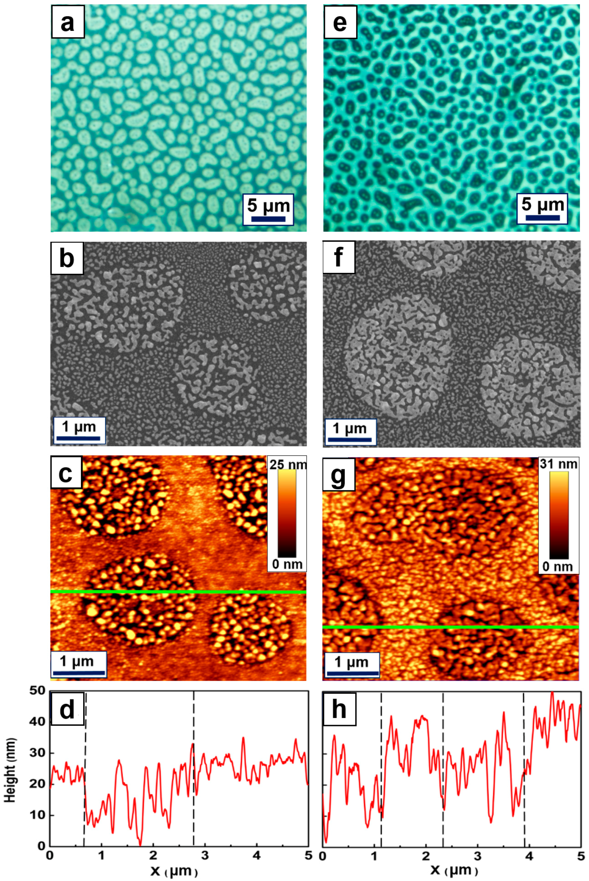
Figure 4.
(a) SEM and (b) AFM images of Sample C.

Figure 5.
(a–c): Fabrication at an annealing temperature of 400 °C using a concentration of the colloidal solution of 60, 100, and 120 mg/mL, respectively; (d–f): Fabrication using a concentration of 100 mg/mL of the colloidal solution and an annealing temperature of 200, 400, and 500 °C, respectively.
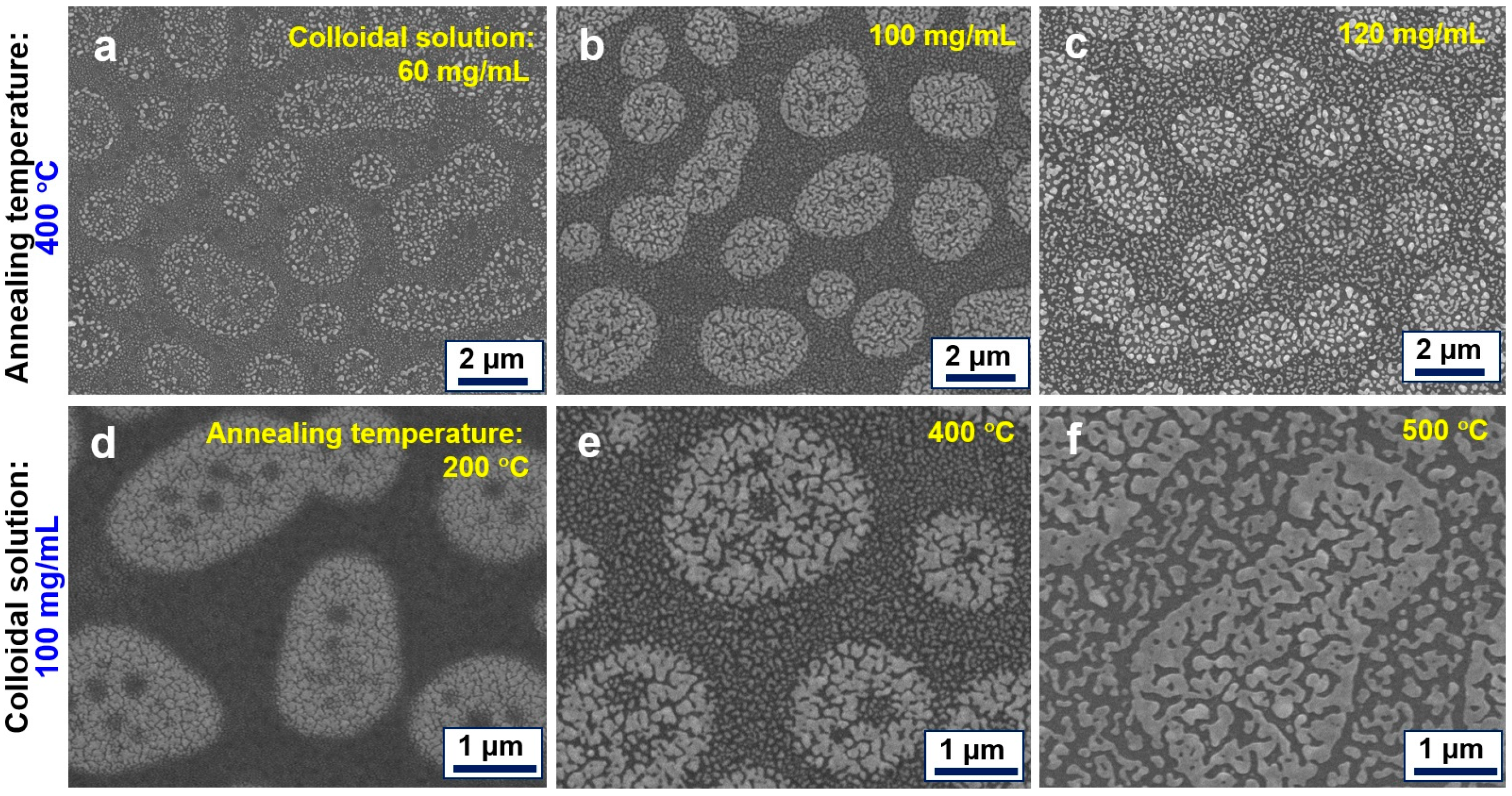
Figure 6.
Measurements of the contact angles of colloidal solution of gold nanoparticles with a concentration of 100 mg/mL in xylene dropped onto the surfaces of (a) F8BT; (b) PFB; and F8BT:PFB blend films before (c) and after (d) being treated using oxygen plasma.
Figure 6.
Measurements of the contact angles of colloidal solution of gold nanoparticles with a concentration of 100 mg/mL in xylene dropped onto the surfaces of (a) F8BT; (b) PFB; and F8BT:PFB blend films before (c) and after (d) being treated using oxygen plasma.

Figure 7.
Optical extinction spectra measured on Samples A (red), B (black, solid), and C (black, dashed). Inset: a local SEM image on Sample A with the scale bar denoting 1 μm.
Figure 7.
Optical extinction spectra measured on Samples A (red), B (black, solid), and C (black, dashed). Inset: a local SEM image on Sample A with the scale bar denoting 1 μm.
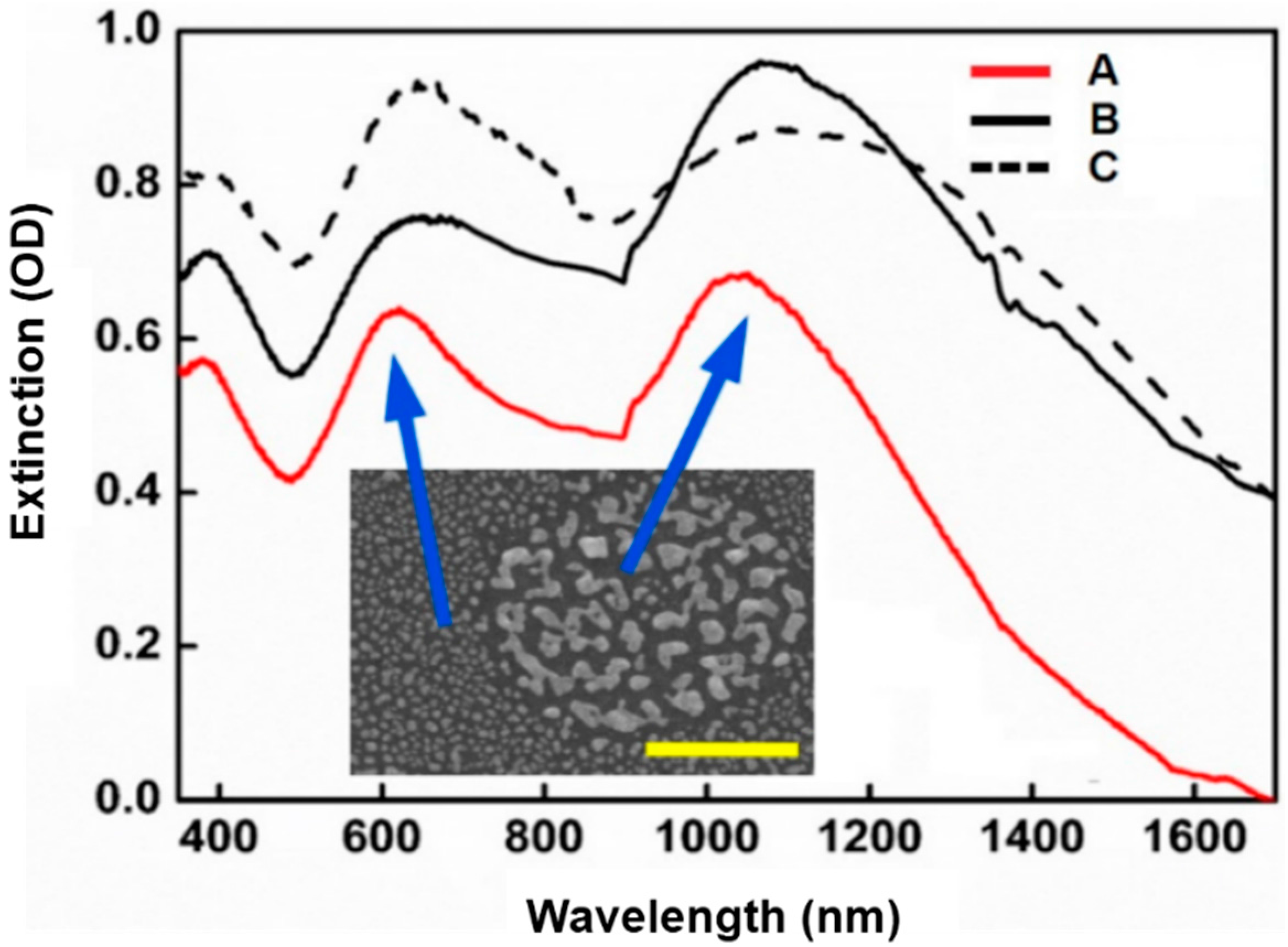
Figure 8.
Dark-field optical microscopic images for (a) Sample A; (b) Sample B; and (c) Sample C.

© 2017 by the authors. Licensee MDPI, Basel, Switzerland. This article is an open access article distributed under the terms and conditions of the Creative Commons Attribution (CC BY) license (http://creativecommons.org/licenses/by/4.0/).
Share and Cite
MDPI and ACS Style
Huang, C.; Zhang, X. Broadband Dual-Phase Plasmons through Metallization of Polymeric Heterojunctions. Metals 2017, 7, 314. https://doi.org/10.3390/met7080314
AMA Style
Huang C, Zhang X. Broadband Dual-Phase Plasmons through Metallization of Polymeric Heterojunctions. Metals. 2017; 7(8):314. https://doi.org/10.3390/met7080314
Chicago/Turabian StyleHuang, Cuiying, and Xinping Zhang. 2017. "Broadband Dual-Phase Plasmons through Metallization of Polymeric Heterojunctions" Metals 7, no. 8: 314. https://doi.org/10.3390/met7080314
Note that from the first issue of 2016, this journal uses article numbers instead of page numbers. See further details here.