Article

Intermetallic Reactions during the Solid-Liquid Interdiffusion Bonding of Bi2Te2.55Se0.45 Thermoelectric Material with Cu Electrodes Using a Sn Interlayer

1
Wire Technology Co., LTD, Taichung 432, Taiwan
2
Institute of Materials Science and Engineering, National Taiwan University, Taipei 106, Taiwan
*
Author to whom correspondence should be addressed.
Metals 2016, 6(4), 92; https://doi.org/10.3390/met6040092
Submission received: 26 February 2016 / Revised: 13 April 2016 / Accepted: 19 April 2016 / Published: 22 April 2016
(This article belongs to the Special Issue Intermetallics 2016)

Abstract

:
The intermetallic compounds formed during the diffusion soldering of a Bi2Te2.55Se0.45 thermoelectric material with a Cu electrode are investigated. For this bonding process, Bi2Te2.55Se0.45 was pre-coated with a 1 μm Sn thin film on the thermoelectric element and pre-heated at 250 °C for 3 min before being electroplated with a Ni barrier layer and a Ag reaction layer. The pre-treated thermoelectric element was bonded with a Ag-coated Cu electrode using a 4 μm Sn interlayer at temperatures between 250 and 325 °C. The results indicated that a multi-layer of Bi–Te–Se/Sn–Te–Se–Bi/Ni3Sn4 phases formed at the Bi2Te2.55Se0.45/Ni interface, ensuring sound cohesion between the Bi2Te2.55Se0.45 thermoelectric material and Ni barrier. The molten Sn interlayer reacted rapidly with both Ag reaction layers to form an Ag3Sn intermetallic layer until it was completely exhausted and the Ag/Sn/Ag sandwich transformed into a Ag/Ag3Sn/Ag joint. Satisfactory shear strengths ranging from 19.3 and 21.8 MPa were achieved in Bi2Te2.55Se0.45/Cu joints bonded at 250 to 300 °C for 5 to 30 min, dropping to values of about 11 MPa for 60 min, bonding at 275 and 300 °C. In addition, poor strengths of about 7 MPa resulted from bonding at a higher temperature of 325 °C for 5 to 60 min.

1. Introduction

Bi2Te2.55Se0.45 intermetallic compound has been widely used as an N-Type thermoelectric (TE) material. For the manufacturing of thermoelectric modules, the TE elements are traditionally soldered with metallic electrodes [1]. A typical example was demonstrated by Chien et al. for the soldering of Bi2Te3/Cu couples using a Sn3Ag0.5Cu alloy [2]. Although satisfactory joints in TE modules can be attained by conventional soldering, they cannot endure temperatures higher than the melting point of the solder alloy. To solve this problem, an additional water heat exchanger is usually required for cooling at the hot end of soldered TE modules industrially applied as power generators or waste heat recyclers. Ritzer et al. further reported that excessive molten solder can wick up the sides of TE pellets and cause electrical shorts between TE couples [3]. Another method for the bonding of TE elements with metallic electrodes is brazing, which uses a filler metal with a melting point higher than 400 °C. The manufactured thermoelectric modules can be operated at temperatures higher than that of soldered joints [4]. However, cracking at the brazed interfaces can occur due to the high thermal stress induced by the solidified filler metal. In addition, the liquid filler metal can strongly diffuse into the thermoelectric element, leading to the degradation of its TE efficiency. Neither the wicking of molten metal nor the risk of short circuits during the soldering process can be prevented in the brazing of TE modules.
An alternate diffusion soldering technique (also called solid-liquid interdiffusion bonding) uses a thin film solder (LT) inserted between the high-melting metallic work pieces or the metallization on certain substrates (HT1 and HT2) that are to be bonded. The LT interlayer, which is molten at low temperatures and acts as a transient liquid phase material, reacts rapidly with the HT1 and HT2 metals to form intermetallic phases. After a short period of solid-liquid interfacial reaction during the diffusion soldering process, the thin film solder (LT) is exhausted and has completely transformed into intermetallic compounds. The melting point of the newly formed intermetallics is much higher than that of the original LT interlayer, so the resulting joints can withstand considerably high temperatures during the operation of the manufactured thermoelectric modules. In fact, diffusion soldering has been applied in the past few decades to the manufacturing of microwave packages, high power devices, thick-film resistors, GaAs/Si wafer packages, and even gold jewelry, as reported by Jacobson and Humpston [5]. Such a novel bonding technique has also been employed by Chuang et al. to join Si chips with ceramic substrates [6,7]. In addition, certain advanced applications, such as those for micro electro mechanical systems (MEMS) packaging [8], semiconductor packaging [9], hybrid joining [10], and hermetic package sealing, have also been reported [11]. The mechanism of the intermetallic reactions was intensively studied by Bader, Gust, and Hieber [12].
Recently, diffusion soldering has been used to bond thermoelectric elements with metallic electrodes. In the studies of Yang et al., Bi0.5Sb1.5Te3 and GeTe thermoelectric materials were bonded with Cu electrodes using the diffusion soldering process at temperatures ranging from 250 to 325 °C with an additional thin-film Sn interlayer [13,14]. In both cases, satisfactory joints with sufficient bonding strengths were obtained. A sound bonding effect was also reported by Chuang et al. for the diffusion soldering of (Pb,Sn)Te thermoelectric elements with Cu electrodes using a Sn interlayer [15]. They further lowered the bonding temperatures for manufacturing, such as the (Pb,Sn)Te thermoelectric module, to a range of 170 °C to 250 °C by changing the Sn thin film interlayer to In [16]. The use of this bonding technique for manufacturing a Bi2Te2.55Se0.45 module with a Cu electrode using a Sn interlayer will be further verified in this work. This study focuses on the intermetallic reactions occurring at the various interfaces of the multilayers in the Bi0.5Sb1.5Te3/Cu joint, diffusion-soldered under various joining conditions and the resultant bonding strengths.

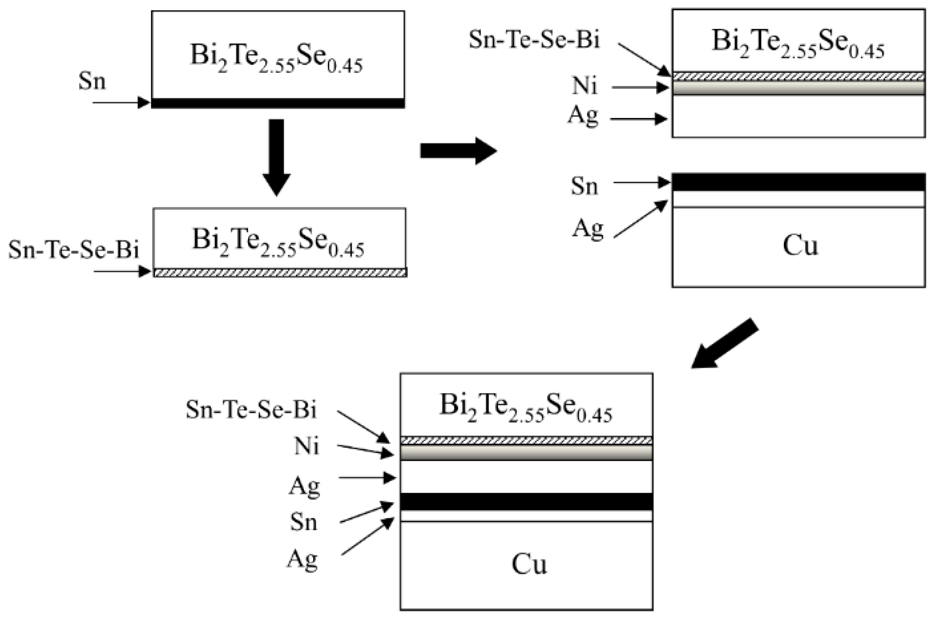
2. Experimental Section

Bi2Te2.55Se0.45 thermoelectric material with an average composition (at. %) of Bi:Te:Se = 40:49:11 was vacuum-melted at 750 °C and then zone-refined with a speed of 1 mm/min. For the preparation of diffusion-soldered Bi2Te2.55Se0.45 specimens with Cu electrodes, the Bi2Te2.55Se0.45 ingot was cut into TE elements with a size of 3 × 3 × 3 mm and ground with 4000 Grit SiC paper. The bonding surfaces of these Bi2Te2.55Se0.45 TE specimens were pre-coated with a 1 μm Sn thin film and pre-heated at 250 °C for 3 min, after which they were electroplated with a ~4 μm Ni diffusion barrier layer and a 10 μm Ag reaction layer. The Cu electrodes were also electroplated with a ~4 μm Ag layer and a 4 μm Sn interlayer. The pre-treated Bi2Te2.55Se0.45 thermoelectric element and Cu electrode were assembled in a vacuum furnace of 5.3 × 10⁻⁴ Pa and subsequently heated for the diffusion soldering process under an external pressure of 3 MPa, as shown in Figure 1. The Bi2Te2.55Se0.45 /Cu assemblies were bonded at temperatures ranging from 250 to 325 °C for various times between 5 and 60 min. The diffusion-soldered Bi2Te2.55Se0.45/Cu joints were cross-sectioned, ground with 4000 Grit SiC paper, and polished with 1 and 0.3 μm Al2O3 powders. The morphologies and compositions of the intermetallic compounds that formed at the interfaces were analyzed via scanning electron microscopy (SEM) (JEOL JSM-6510, JEOL Ltd., Tokyo, Japan) and energy dispersive X-ray spectroscopy (EDX) (Oxford Instruments, Abingdon, UK). In addition, the growth of interfacial intermetallics was directly estimated from the images in SEM. The average value of a minimum of 30 measurements for each diffusion-soldered specimen was determined to signify the intermetallic thickness (X).
The bonding strengths of various Bi2Te2.55Se0.45/Cu joints were shear-tested with a DAGE 4000 Bond Tester (Nordson DAGE, Aylesbury, UK) at a speed of 0.3 mm/s. The fractured surfaces of the shear-tested specimens were observed via SEM. For the measurements of intermetallic thicknesses and shear strengths, at least 3 specimens were employed for each bonding condition. The standard deviations (σ) for all measurements were calculated from the average values (μ) of measured data (xi) and plotted as the error bars of the experimental quantitative results:
σ = 1 N i = 1 N ( x i μ ) 2
where N is the number of measurements.

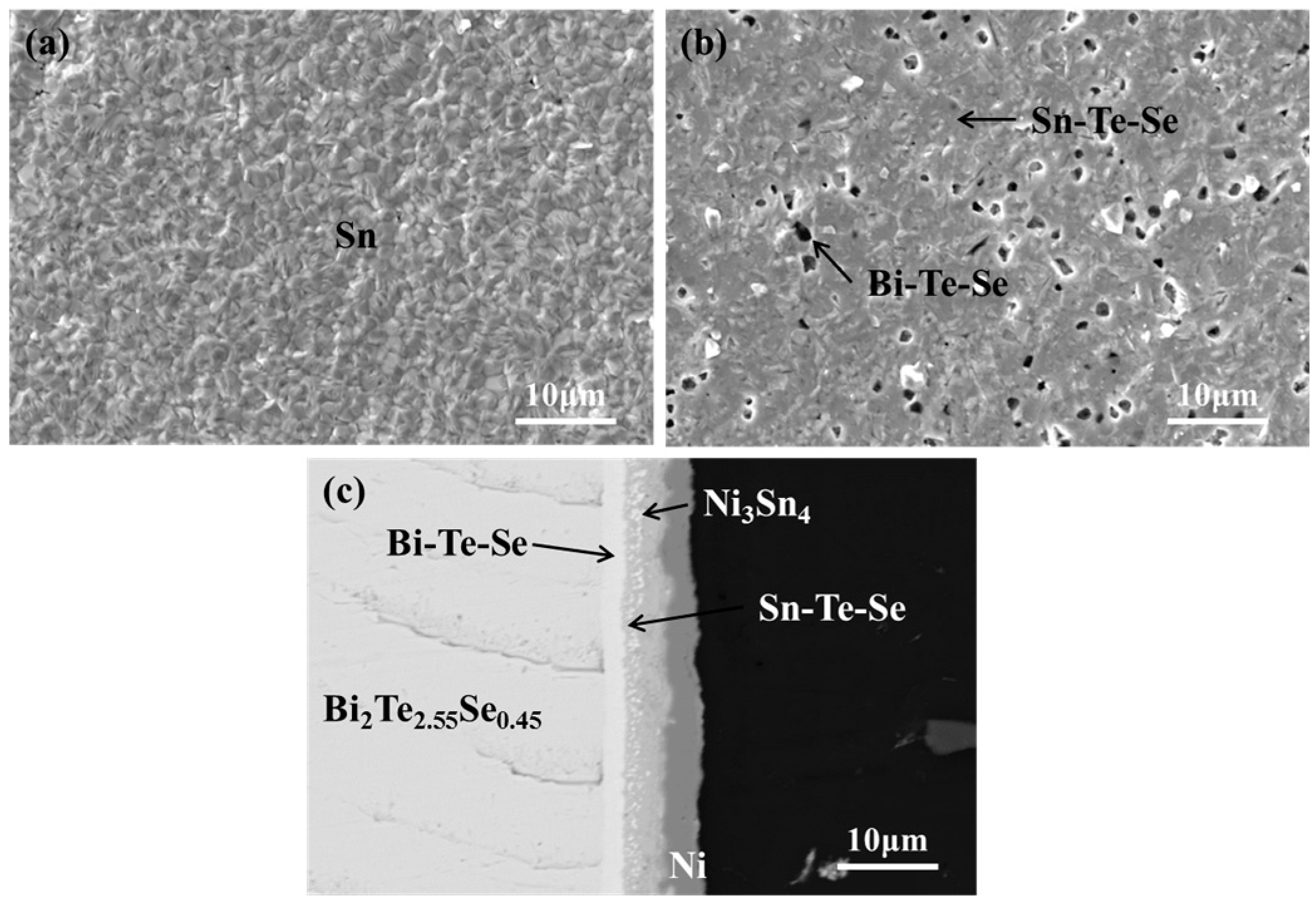
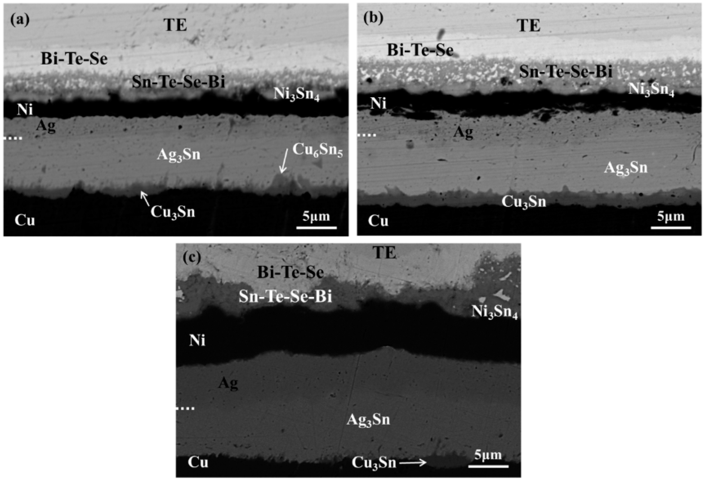
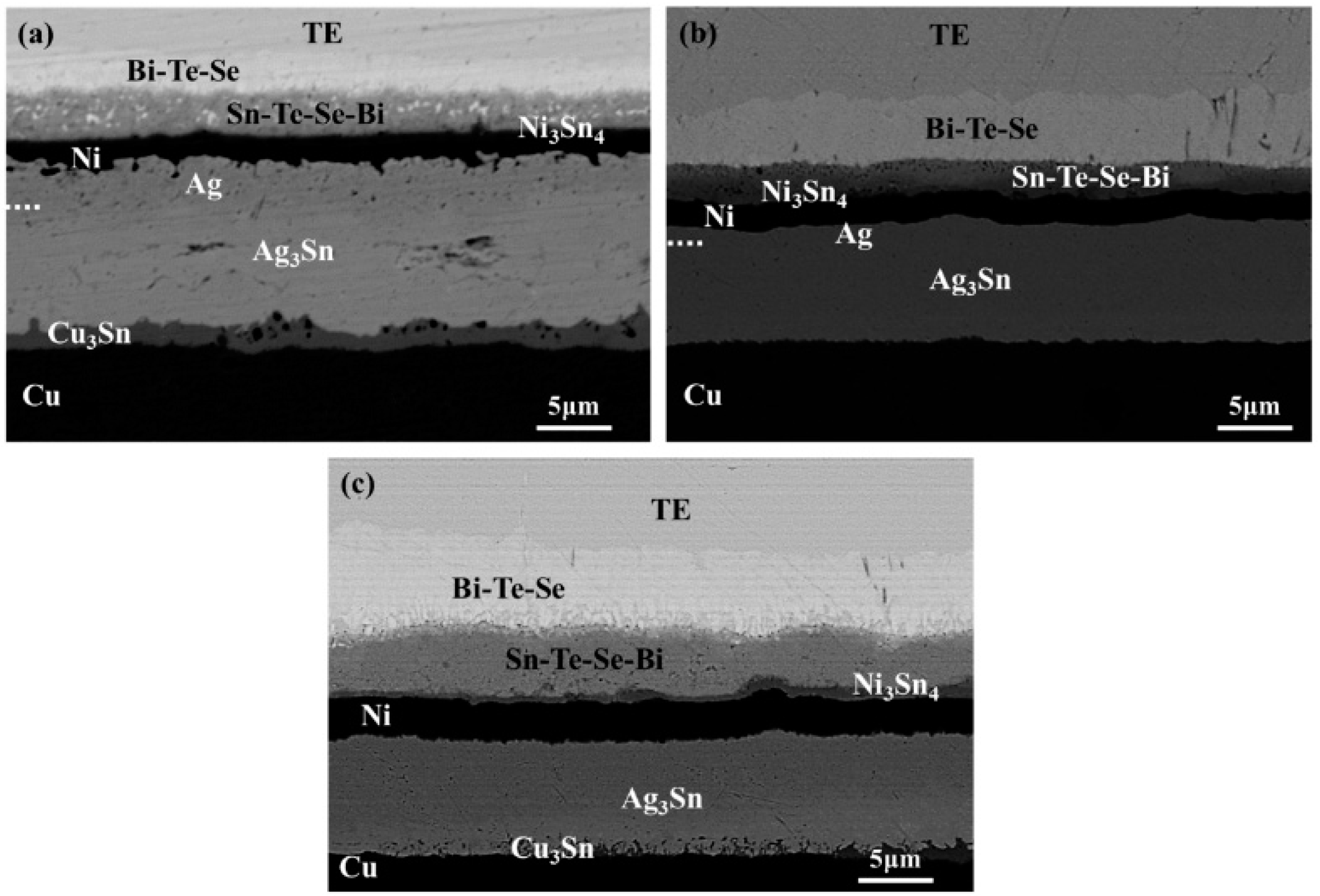
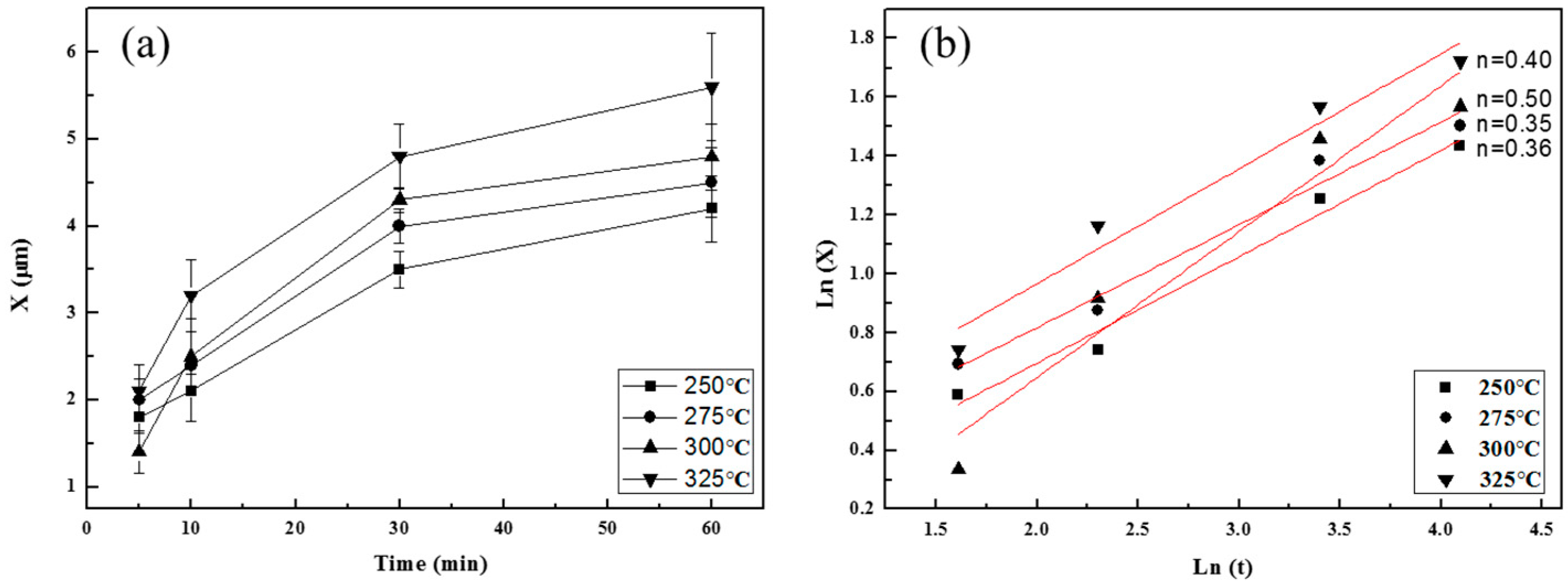
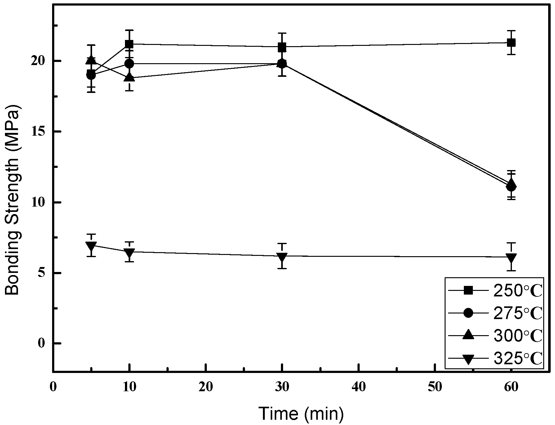
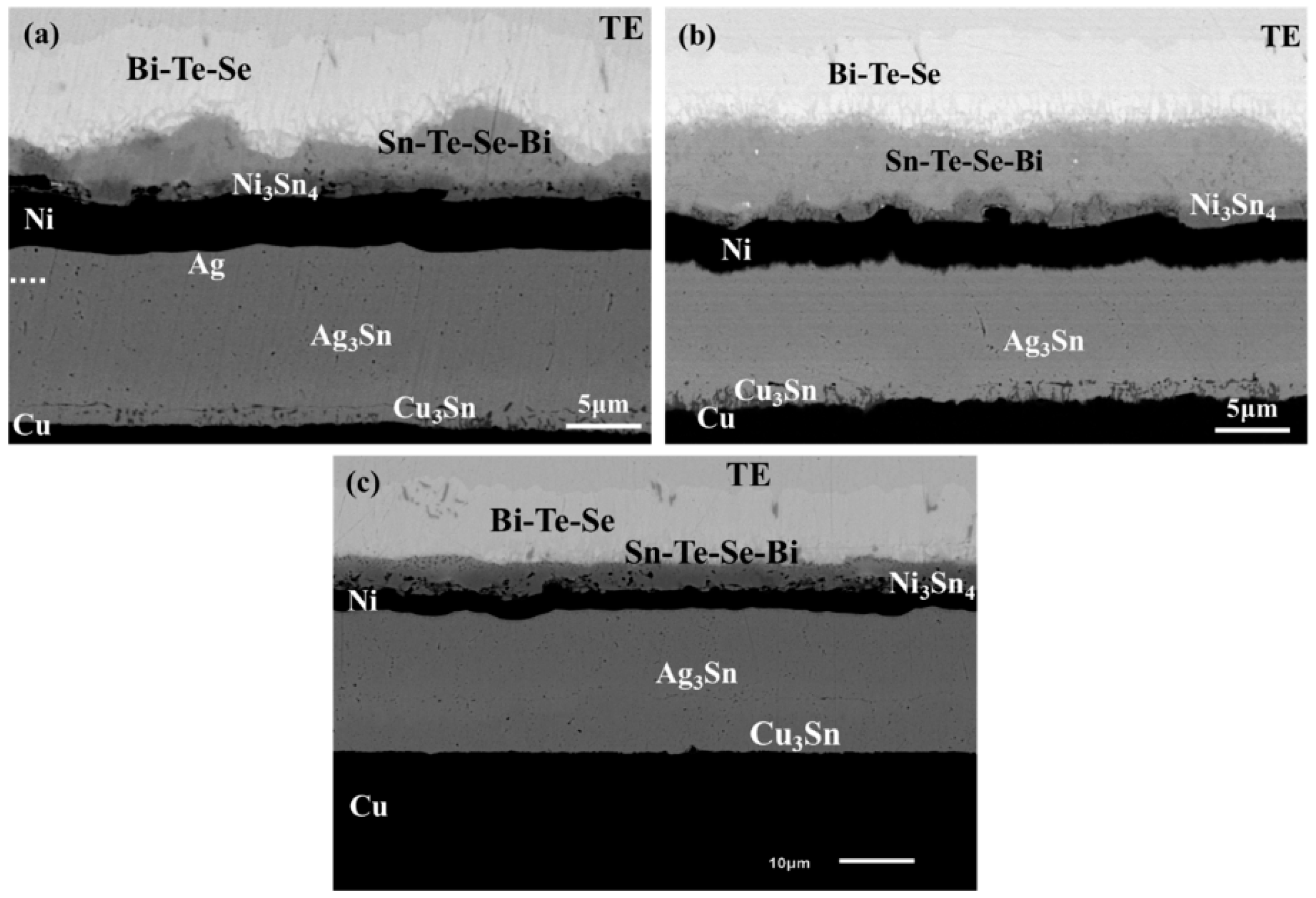
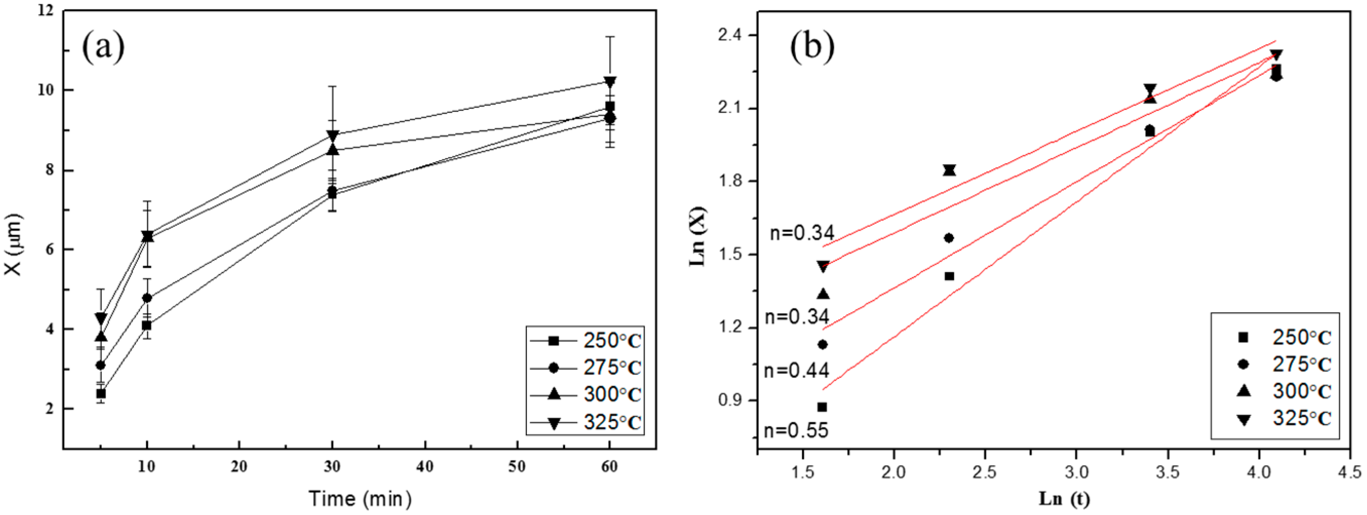
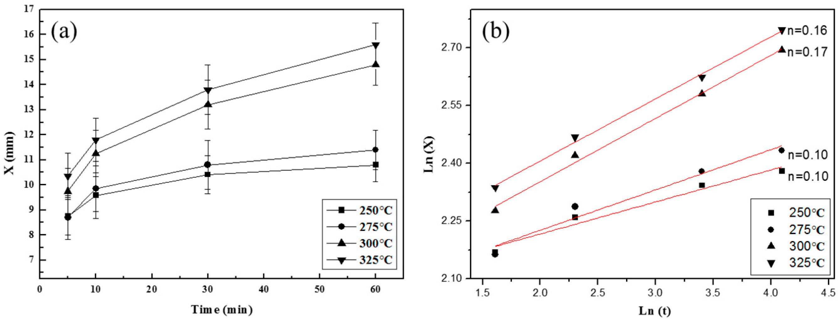
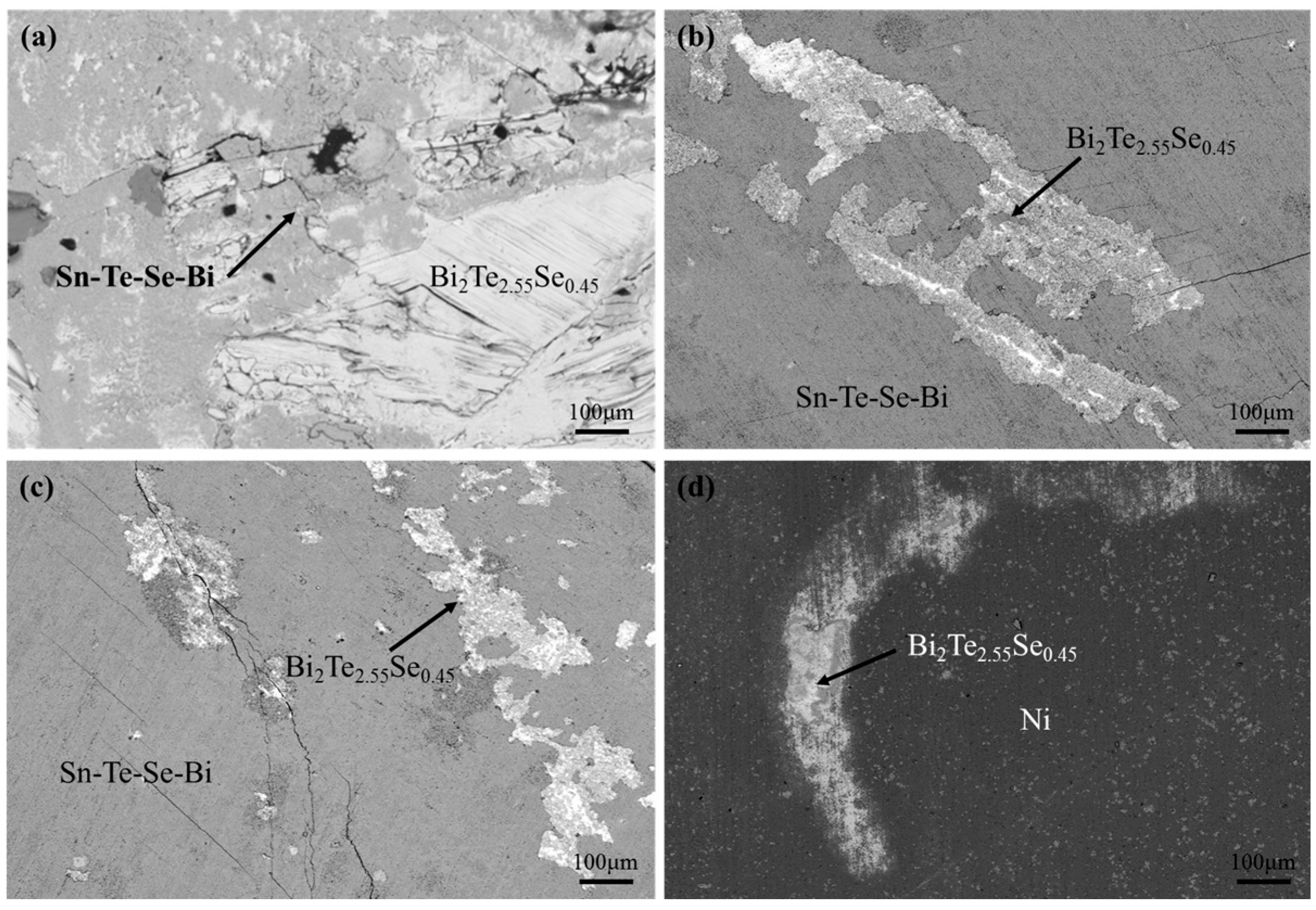
3. Results and Discussion

Figure 2 shows that, after pre-coating the Sn layer (Figure 2a) and directly heating it at 250 °C for 3 min, the Bi2Te2.55Se0.45 thermoelectric material reacted with the thin-film Sn layer to form a mixed phase (shown in Figure 2b) consisting of many Bi-rich particles with a composition (at. %) of Bi:Te:Se = 55:40:5 embedded in the Sn-rich matrix of Sn:Te:Se = 52:44:4.
The compositions of the Bi-rich particles and Sn-rich matrix corresponded to the BiTe and SnTe intermetallic phases. It is obvious that the Te and Se elements in the Bi2Te2.55Se0.45 thermoelectric material reacted with the pre-coated Sn film to form a continuous Sn–Te–Se layer. The result is consistent with the report of Chiu et al. that a SnTe intermetallic phase with a B1 crystal structure mainly formed in a Bi–Sn–Te ternary system [17]. In this study, certain Te lattices in the SnTe phase were replaced by Se atoms. The Bi atoms in the Bi2Te2.55Se0.45 thermoelectric material remained after the reaction, appearing as Bi-rich islands in Figure 2b. For comparison, the Bi2Te2.55Se0.45 thermoelectric material was also coated with a 1 μm Sn thin film and a ~4 μm Ni barrier layer and then heated at 250 °C for 3 min. Figure 2c shows that a thick Ni3Sn4 intermetallic compound appeared between the Ni and Sn–Te–Se layers in this case. It is obvious that the formation of Ni3Sn4 intermetallics is preferential to that of Sn–Te–Se phase during the interfacial reaction between Ni and Bi2Te2.55Se0.45 thermoelectric materials.
To prevent the over-consumption of the Ni barrier layer, a pre-treatment process for Bi2Te2.55Se0.45 thermoelectric material before diffusion soldering was selected. A 1 μm Sn thin film was electroplated on the material, and the composite was directly heated at 250 °C for 3 min. The pre-treated Bi2Te2.55Se0.45 thermoelectric material was then coated with an additional Ni barrier layer and Ag reaction layer with thicknesses of about 4 μm and 10 μm, respectively. The composite was subsequently bonded with a Ag-coated Cu electrode using a Sn interlayer in a vacuum furnace of 5.3 × 10⁻⁴ Pa at temperatures ranging from 250 °C to 325 °C for various times between 5 and 60 min under an external pressure of 3 MPa. Micrographs of the interfacial reactions during such a diffusion soldering process at 250 °C for various times are shown in Figure 3. It can be observed that a Ni3Sn4 intermetallic layer appeared before the Ni barrier layer. In addition, a very thin layer of Bi–Te–Se phase (white in color) with a composition (at. %) of Bi:Te:Se = 52:36:12 formed on the surface of the Bi2Te2.55Se0.45 thermoelectric material. Between the Ni3Sn4 intermetallic layer and the Bi–Te–Se phase, a thick Sn-rich layer (gray in color) embedded with Bi-rich islands (white in color) can be observed. The compositions (at. %) were Sn:Te:Se:Bi = 43:36:10:11 and Bi:Te:Se:Sn = 54:38:5:3, respectively. Increasing the bonding times, the Ni barrier layer reacted with the Sn-rich phase to form a Ni3Sn4 intermetallic layer, improving the cohesion between Ni barrier and Bi2Te2.55Se0.45 thermoelectric material. Underneath the Ni barrier layers, the pre-coated Ag reaction layers remained after the diffusion soldering process, while the Sn thin film interlayer was exhausted and reacted with part of the Ag layer to transform into a Ag3Sn intermetallic layer. Since the Ag3Sn intermetallic phase has a melting point of 480 °C, the diffusion-soldered Bi2Te2.55Se0.45 TE modules in this study can be applied at temperatures much higher than that for conventional soldered modules. Figure 3 also reveals that a Cu3Sn intermetallic phase formed at the interface between the Ag3Sn intermetallic layer and the Cu electrode.
It is worth mentioning that sound interfaces were obtained in the Bi2Te2.55Se0.45/Cu joints bonded in this study, contrary to the report of Bader et al., which voids frequently occurred at the interface of diffusion-soldered Ni/Sn/Ni and Cu/Sn/Cu specimens [12]. This difference may be explained by the external pressure of 3 MPa employed in this work, which is higher than that used in the work of Bader et al. In addition, it is postulated that fewer voids occur inherently during the intermetallic reaction at the Ag/Sn/Ag interface than during reactions at Ni/Sn/Ni and Cu/Sn/Cu interfaces. The result provides a beneficial effect of eliminating voids at the diffusion-soldered Ni/Sn/Ni or Cu/Sn/Cu interfaces through the insertion of an Ag3Sn intermetallic layer between the Ni-Sn and Cu-Sn intermetallic compounds [18].
From Figure 3, it is obvious that the Sn–Te–Se–Bi, Ni3Sn4, and Ag3Sn intermetallic compounds in the Bi2Te2.55Se0.45/Cu joints, bonded with diffusion soldering at 250 °C, grew with bonding times of 5 min to 30 min. Increasing the bonding temperature to 300 °C further increased the thickness of these intermetallic compounds, as shown in Figure 4. Similar growth of the intermetallics can be observed in Figure 5, which shows the results of the diffusion soldering of Bi2Te2.55Se0.45 thermoelectric material with a Cu electrode at various temperatures from 250 to 325 °C for 60 min. Similar satisfactory interfaces without voids can be achieved in the diffusion-soldered Bi2Te2.55Se0.45/Cu joints for such a long bonding time. Although the pre-coated Ag reaction layers underneath the Ni barrier layers have been exhausted after diffusion soldering at temperatures higher than 300 °C for times longer than 30 min, as shown in Figure 4c and Figure 5b,c, sound interfaces without any voids appear between Ag3Sn intermetallic compounds and Ni barrier layers.
The thicknesses (X) of these intermetallic layers that formed at various temperatures were measured and are plotted in Figure 6a–Figure 8a as a function of bonding time (t). For the kinetics analyses, LnX versus Lnt is plotted in Figure 6b–Figure 8b. The growth exponents (n) for Sn–Te–Se–Bi intermetallic layers calculated from the slopes of straight lines in Figure 6b ranged from 0.34 to 0.55. Similarly, the n values of and Ni3Sn4 growth calculated from the plots in Figure 7b ranged from 0.35 to 0.50. It is evidenced that the growth exponents (n) for both the Sn–Te–Se–Bi and the Ni3Sn4 intermetallics were close to that of a diffusion-controlled reaction (n = 0.5). However, the growth exponents (n) for the Ag3Sn intermetallic layers, as shown in Figure 8b, ranged from 0.10 to 0.17, which are inconsistent with that of a diffusion mechanism. This discrepancy can be attributed to the release of partial Sn atoms in the Ag3Sn intermetallic layers to react with the Cu electrodes to form Cu3Sn intermetallic compounds after the exhaust of the Ag films on the Cu electrodes.
The shear strengths of the Bi2Te2.55Se0.45/Cu joints, diffusion-soldered at 250 to 300 °C, ranged between 19.3 and 21.8 MPa, as shown in Figure 9. These strengths are much higher than the maximal strength of 10.7 MPa for the Bi0.5Sb1.5Te3/Cu joints bonded in the study of Yang et al. under the same conditions [13]. The superior bonding of Bi2Te2.55Se0.45/Cu relative to that of Bi0.5Sb1.5Te3/Cu joints is attributed to the mechanical strength of the Bi2Te2.55Se0.45 thermoelectric material, which is superior to that of Bi0.5Sb1.5Te3 due to the embrittlement of the Sb element in BiTe material. In this case, the shear-tested Bi2Te2.55Se0.45/Cu joints fractured through the interior of the Bi2Te2.55Se0.45 thermoelectric material and Sn–Te–Se–Bi intermetallics layer, as shown in Figure 10a. However, lengthening the bonding time to 60 min at 275 and 300 °C decreased the shear strength to about 11 MPa. In addition, Figure 9 also reveals low strengths of about 7 MPa for the Bi2Te2.55Se0.45/Cu joints bonded at 325 °C for various times. The micrographs in Figure 10b,c, for the shear-tested specimens bonded at 275 and 300 °C for 60 min, show that the Bi2Te2.55Se0.45/Cu joints, having lower bonding strengths of about 11 MPa, also fractured through the interior of the Bi2Te2.55Se0.45 thermoelectric material and the Sn–Te–Se–Bi intermetallics layer, similar to the case in Figure 10a. However, the amount of Bi2Te2.55Se0.45 thermoelectric materials remaining in the fractography of these poorly bonded specimens was much less than that in Figure 10a, and many cracks appeared in the Sn–Te–Se–Bi intermetallic phase. Furthermore, diffusion soldering at 325 °C resulted in the fracture of shear-tested Bi2Te2.55Se0.45/Cu joint through the interior of the Bi2Te2.55Se0.45 thermoelectric material and Sn–Te–Se–Bi/Ni interface, as shown in Figure 10d. The insufficient bonding effect of Bi2Te2.55Se0.45/Cu joints at 325 °C can be correlated to the over-growth of the Sn–Te–Se–Bi intermetallics and preferential cracking at Sn–Te–Se–Bi/Ni interface during the shear tests. In addition, the cooling of Bi2Te2.55Se0.45/Cu joints from 325 °C to room temperature can cause large thermal stress and exacerbate the decay of bonding strength. Similarly, the thickening of Sn–Te–Se–Bi intermetallics and high thermal stress can also occur in the Bi2Te2.55Se0.45/Cu joints after diffusion soldering at 275 and 300 °C for 60 min, leading to the drastic drop of shear strengths in Figure 9. For the bonding at 250 °C, such detrimental effects are negligible, and the shear strengths of Bi2Te2.55Se0.45/Cu joints can remain unchanged as shown in Figure 9.
Furthermore, the reliability of the diffusion-soldered Bi2Te2.55Se0.45/Cu joints in correlation to the thermal stress formed in the multilayer structure of intermetallic compounds is considered. The coefficients of thermal expansion (CTE) of Ni3Sn4, Cu3Sn, Ni and Cu as reported by Frear et al. [19] are 13.7, 19.0, 12.9, and 17.1, respectively. The CTE value of the Sn–Te–Se–Bi intermetallic compound could be lower than that of pure Sn (23.0). The size of Bi2Te2.55Se0.45 thermoelectric elements in this study is 3 × 3 × 3 mm. It is known that the optimized thermoelectric temperature of a Bi2Te2.55Se0.45 module is 120 to 150 °C. In this case, the thermal stress caused by the CTE mismatch between various materials in such small Bi2Te2.55Se0.45/Cu joints results in a slight risk of failure during the operation of this thermoelectric module.

4. Conclusions

Bi2Te2.55Se0.45 thermoelectric modules can be manufactured by the diffusion soldering method using a 4 μm Sn thin film interlayer inserted between the Ag/Ni-coated Bi2Te2.55Se0.45 and Ag-coated Cu electrode. For this purpose, pre-coating a 1 μm Sn thin film on the thermoelectric element and heating at 250 °C for 3 min enhances the cohesion between the Bi2Te2.55Se0.45 and Ni barrier. After diffusion soldering, a multi-layer of Bi–Te–Se, Sn–Te–Se–Bi, and Ni3Sn4 intermetallic phases can be found at the Bi2Te2.55Se0.45/Ni interface. In addition, the employment of Ag interlayers in this Ni/Ag/Sn/Ag/Cu bonding system eliminates the voids that frequently appear at the Ni/Sn and Cu/Sn interfaces. Shear tests for the Bi2Te2.55Se0.45/Cu joints, diffusion-soldered at 250 to 300 °C for 5 to 30 min, resulted in satisfactory bonding strengths ranging from 19.3 to 21.8 MPa. However, diffusion soldering at 275 and 300 °C for 60 min caused the over-growth and cracking of the Sn–Te–Se–Bi intermetallic layer, which resulted in lower shear strengths of about 11 MPa. The bonding strengths of Bi2Te2.55Se0.45/Cu joints further decayed to values of about 7 MPa after diffusion soldering at 325 °C for various times.

Acknowledgments

This study was sponsored by the Small Business Innovation Research (SBIR) program of the Ministry of Economic Affairs (MOEA), Taiwan, under Grant No.1Z1041847, and by the industrial and academic cooperation program of Wire Technology Co. and the Ministry of Science and Technology, Taiwan, under Grant No. MOST 103-2622-E-002-012-CC2.

Author Contributions

C.H. Chuang conceived and designed the SLID bonding processes for thermoelectric modules, analyzed the interfacial reactions and wrote the paper. Y.C. Lin and C.W. Lin prepared the thermoelectric material, performed the bonding experiments and measured the bonding strengths.

Conflicts of Interest

The authors declare no conflict of interest.

References

  1. Zhang, H.; Jing, H.Y.; Han, Y.D.; Xu, L.Y. Interfacial reaction between n-and p-type thermoelectric materials and SAC305 solders. J. Alloy. Compd. 2013, 576, 424–431. [Google Scholar] [CrossRef]
  2. Chien, P.Y.; Yeh, C.H.; Hsu, H.H.; Wu, A.T. Polarity Effect in a Sn3Ag0.5Cu/Bismuth Telluride Thermoelectric System. J. Electron. Mater. 2014, 43, 284–289. [Google Scholar] [CrossRef]
  3. Ritzer, T.M.; Lau, P.G.; Bogard, A.D. A Critical Evaluation of Today's Thermoelectric Modules. In Proceedings of the 16th International Conference on Thermoelectrics, Dresden, Germany, 26–29 August 1997; pp. 619–623.
  4. Zybala, R.; Wojciechowski, K.T.; Schmidt, M. Junctions and Diffusion Barriers for High Temperature Thermoelectric Modules. Mater. Ceram./Ceram. Mater. 2010, 62, 481–485. [Google Scholar]
  5. Jacobson, D.M.; Humpston, G. Diffusion Soldering. Solder. Surf. Mt. Technol. 1992, 10, 27–32. [Google Scholar] [CrossRef]
  6. Chuang, T.H.; Lin, H.J.; Tsao, C.W. Intermetallic compounds formed during diffusion soldering of Au/Cu/Al2O3 and Cu/Ti/Si with Sn/In interlayer. J. Electron. Mater. 2006, 35, 1566–1570. [Google Scholar] [CrossRef]
  7. Liang, M.W.; Hsieh, T.E.; Chang, S.Y.; Chuang, T.H. Thin-film reactions during diffusion soldering of Cu/Ti/Si and Au/Cu/Al2O3 with Sn interlayers. J. Electron. Mater. 2003, 32, 952–956. [Google Scholar] [CrossRef]
  8. Welch, W.C.; Chae, J.; Najafi, K. Transfer of metal MEMS packages using a wafer-level solder transfer technique. IEEE Trans. Adv. Packag. 2005, 28, 643–649. [Google Scholar] [CrossRef]
  9. Made, R.I.; Gan, C.L.; Yan, L.L.; Yu, A.; Yoon, S.W.; Lau, J.H.; Lee, C.K. Study of Low-Temperature Thermocompression Bonding in Ag-In Solder for Packaging Applications. J. Electron. Mater. 2009, 38, 365–371. [Google Scholar] [CrossRef]
  10. Li, J.F.; Agyakwa, P.A.; Johnson, C.W. Kinetics of Ag3Sn growth in Ag-Sn-Ag system during transient liquid phase soldering process. Acta Mater. 2010, 58, 3429–3443. [Google Scholar] [CrossRef]
  11. Yan, L.L.; Lee, C.K.; Yu, D.Q.; Yu, A.B.; Choi, W.K.; Lau, J.H.; Yoon, S.U. A Hermetic Seal Using Composite Thin-Film In/Sn Solder as an Intermediate Layer and Its Interdiffusion Reaction with Cu. J. Electron. Mater. 2009, 38, 200–207. [Google Scholar] [CrossRef]
  12. Bader, S.; Gust, W.; Hieber, H. Rapid formation of intermetallic compounds interdiffusion in the Cu-Sn and Ni-Sn systems. Acta Metall. Mater. 1995, 43, 329–337. [Google Scholar]
  13. Yang, C.L.; Lai, H.J.; Hwang, J.D.; Chuang, T.H. Diffusion Soldering of Bi0.5Sb1.5Te3 Thermoelectric Material with Cu Electrode. J. Mater. Eng. Perform. 2013, 22, 2029–2037. [Google Scholar] [CrossRef]
  14. Yang, C.L.; Lai, H.J.; Hwang, J.D.; Chuang, T.H. Diffusion Soldering of Pb-Doped GeTe Thermoelectric Modules with Cu Electrodes Using a Thin-Film Sn Interlayer. J. Electron. Mater. 2012, 42, 359–365. [Google Scholar] [CrossRef]
  15. Chuang, T.H.; Lin, H.J.; Chuang, C.H.; Yeh, W.T.; Hwang, J.D.; Chu, H.S. Solid Liquid Interdiffusion Bonding of (Pb, Sn)Te Thermoelectric Modules with Cu Electrodes Using a Thin-Film Sn Interlayer. J. Electron. Mater. 2014, 43, 4610–4618. [Google Scholar] [CrossRef]
  16. Chuang, T.H.; Yeh, W.T.; Chuang, C.H.; Hwang, J.D. Improvement of bonding strength of a (Pb, Sn)Te–Cu contact manufactured in a low temperature SLID-bonding process. J. Alloy. Compd. 2014, 613, 46–54. [Google Scholar] [CrossRef]
  17. Chiu, C.N.; Wang, C.H.; Chen, S.W. Interfacial Reactions in the Sn–Bi/Te Couples. J. Electron. Mater. 2007, 37, 40–44. [Google Scholar] [CrossRef]
  18. Chang, J.Y.; Chang, T.C.; Chuang, T.H.; Lee, C.Y. Dual-Phase Intermetallic Interconnections Structure and Method of Fabricating the Same. U.S. Patent 8,742,600 B2, 3 June 2014. [Google Scholar]
  19. Frear, D.R.; Burchett, S.N.; Morgan, H.S.; Lau, J.H. The Mechanics of Solder Alloy Interconnects; Van Nostrand Reinhold: New York, NY, USA, 1994; p. 60. [Google Scholar]
Figure 1. The schematic presentation of the diffusion soldering process for the bonding of Bi2Te2.55Se0.45 thermoelectric materials with Cu electrodes using Sn thin film as a transient liquid phase interlayer.
Metals 06 00092 g001
Figure 2. Surface of Bi2Te2.55Se0.45 thermoelectric material after (a) electroplating with 1 μm Sn film, (b) subsequent heating at 250 °C for 3 min, and (c) pre-coated with Sn/Ni and heated 250 °C for 3 min.
Metals 06 00092 g002
Figure 3. Morphology of intermetallic compounds formed after diffusion soldering between Bi2Te2.55Se0.45 thermoelectric material and the Cu electrode with Sn interlayers at 250 °C for various times: (a) 5 min, (b) 10 min, (c) 30 min.
Metals 06 00092 g003
Figure 4. Morphology of intermetallic compounds formed after diffusion soldering between Bi2Te2.55Se0.45 thermoelectric material and the Cu electrode with Sn interlayers at 300 °C for various times: (a) 5 min, (b) 10 min, (c) 30 min.
Metals 06 00092 g004
Figure 5. Morphology of intermetallic compounds formed after diffusion soldering between Bi2Te2.55Se0.45 thermoelectric material and the Cu electrode with Sn interlayers at various temperatures for 60 min: (a) 250 °C, (b) 300 °C, (c) 325 °C.
Metals 06 00092 g005
Figure 6. Thickness (X) of Sn–Te–Se–Bi phase formed during diffusion soldering of Bi2Te2.55Se0.45 thermoelectric material with Cu electrode using Sn interlayers: (a) X versus t, (b) LnX versus Lnt.
Metals 06 00092 g006
Figure 7. Thickness (X) of Ni3Sn4 intermetallic compound formed during diffusion soldering of Bi2Te2.55Se0.45 thermoelectric material with Cu electrode using Sn interlayers: (a) X versus t, (b) LnX versus Lnt.
Metals 06 00092 g007
Figure 8. Thickness (X) of Ag3Sn intermetallic compound formed during diffusion soldering of Bi2Te2.55Se0.45 thermoelectric material with the Cu electrode using Sn interlayers: (a) X versus t, (b) LnX versus Lnt.
Metals 06 00092 g008
Figure 9. Shear strengths of Bi2Te2.55Se0.45/Cu joints bonded with the diffusion soldering process using a Sn interlayer.
Metals 06 00092 g009
Figure 10. Fractured surfaces of shear-tested Bi2Te2.55Se0.45/Cu joints, diffusion-soldered at various temperatures for 60 min using Sn interlayers: (a) 250 °C, (b) 275 °C, (c) 300 °C, (d) 325 °C.
Metals 06 00092 g010

