Peculiarities of the Twinning in Silicon during Ball Milling in the Presence of Two Different Materials

 ,
, 
Abstract
:1. Introduction
2. Experimental
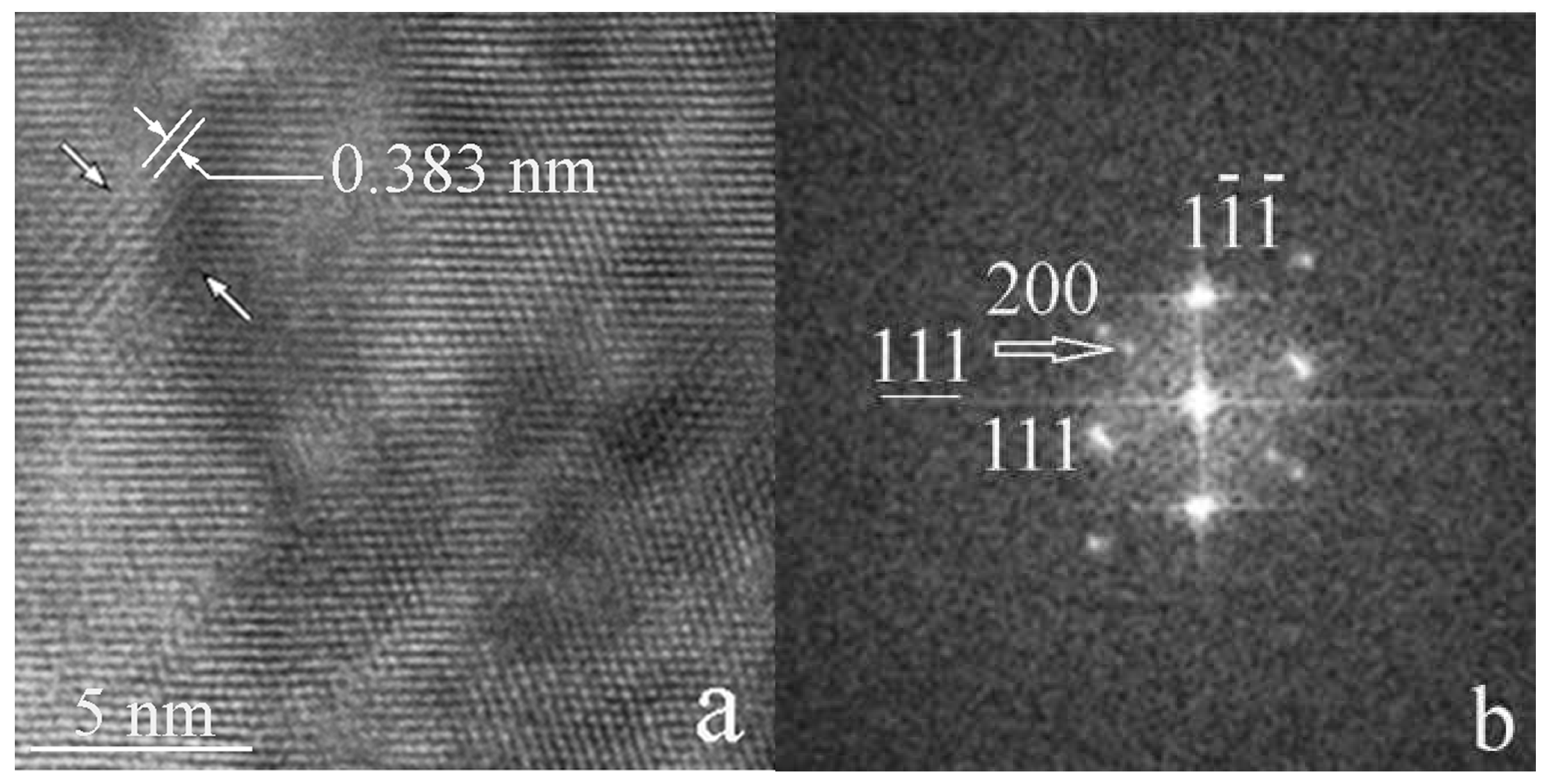
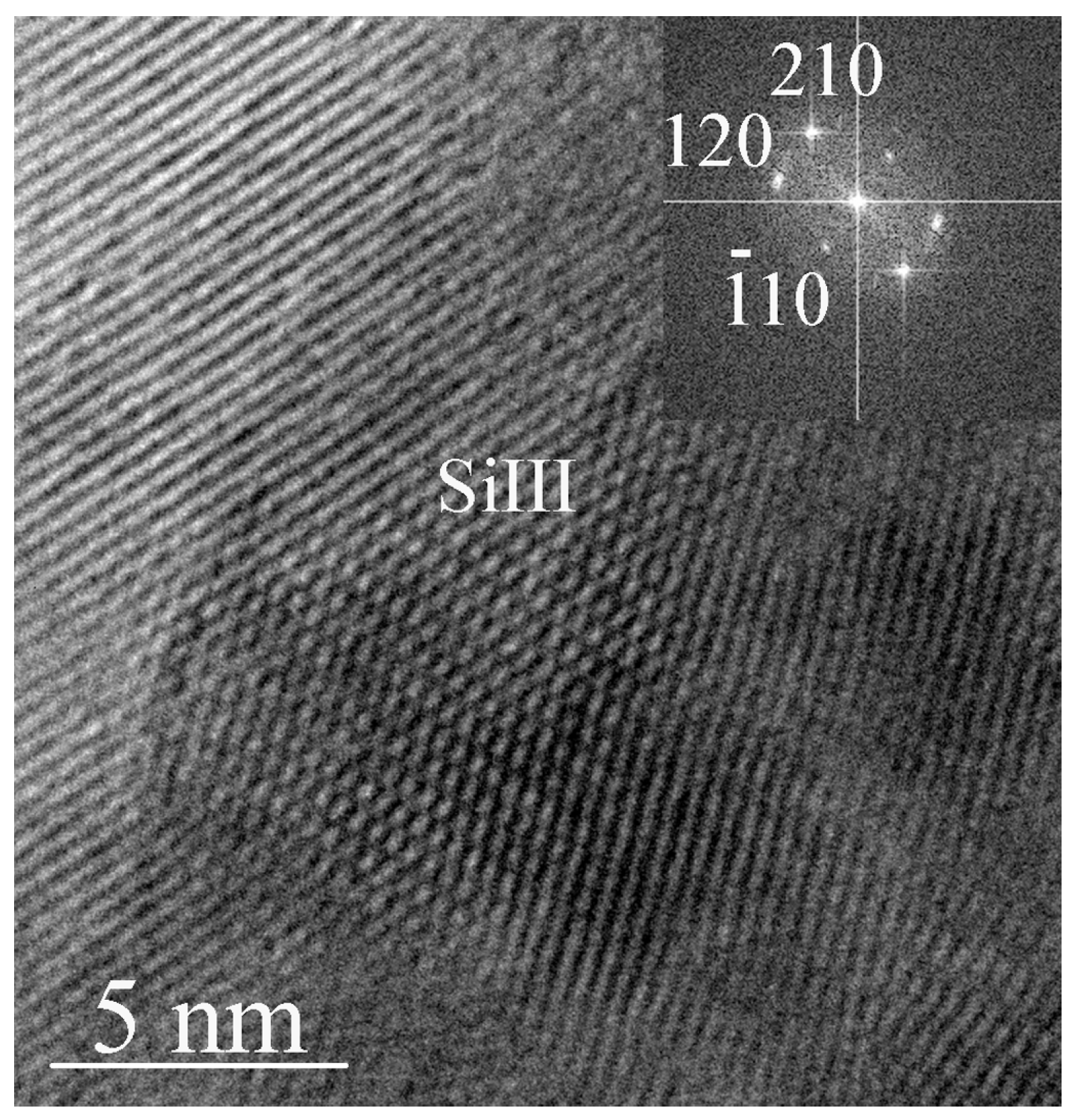
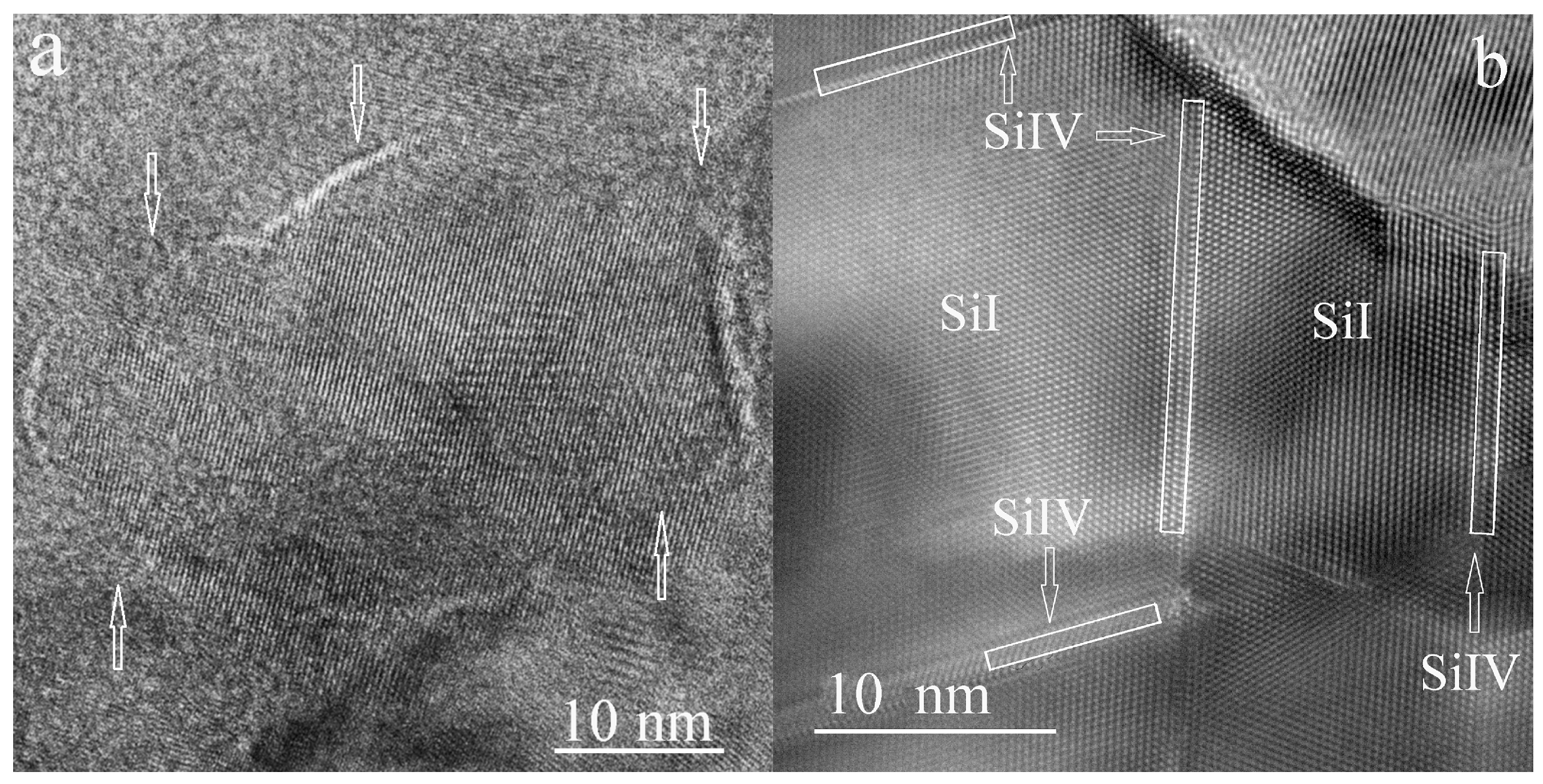
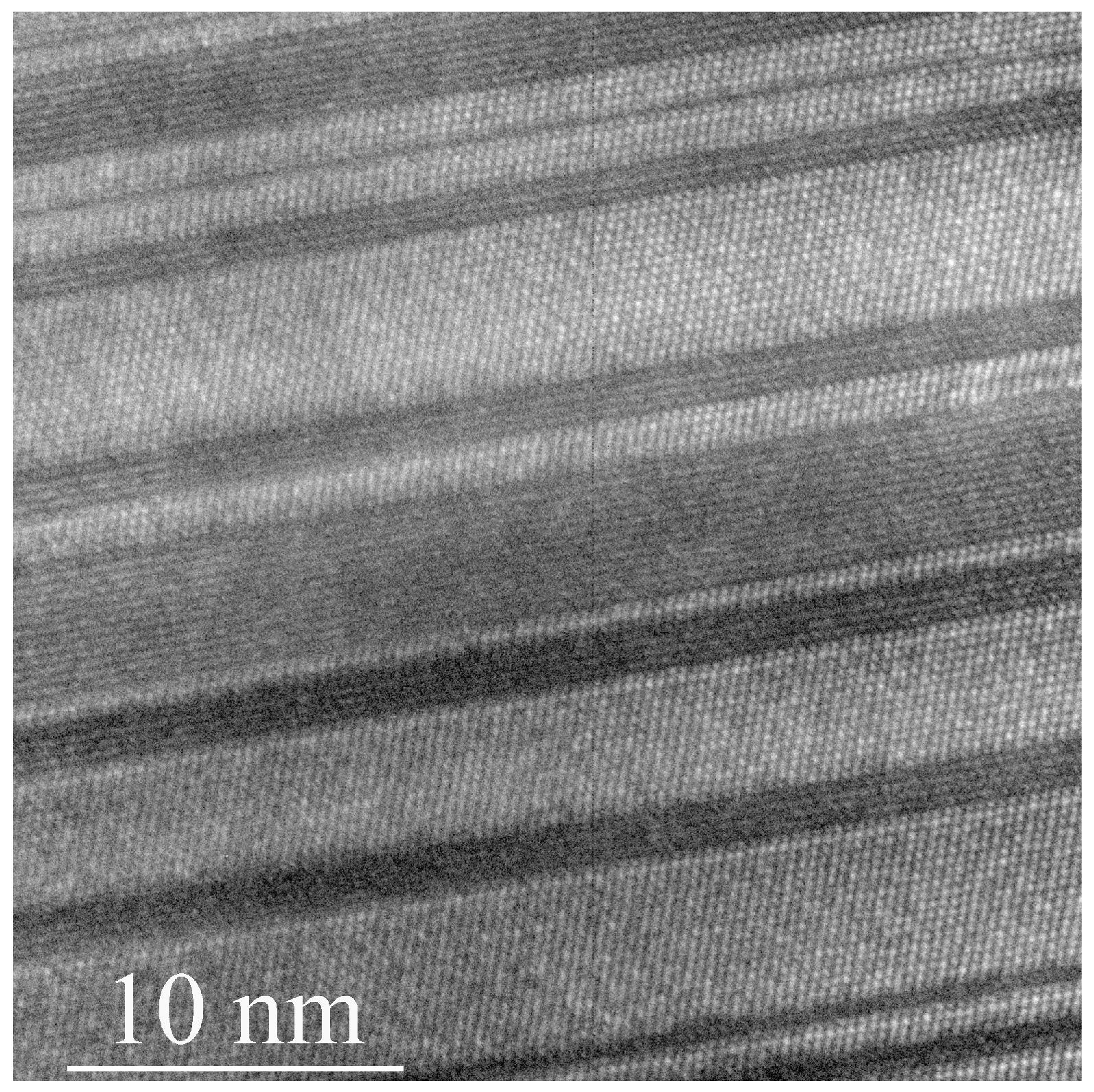
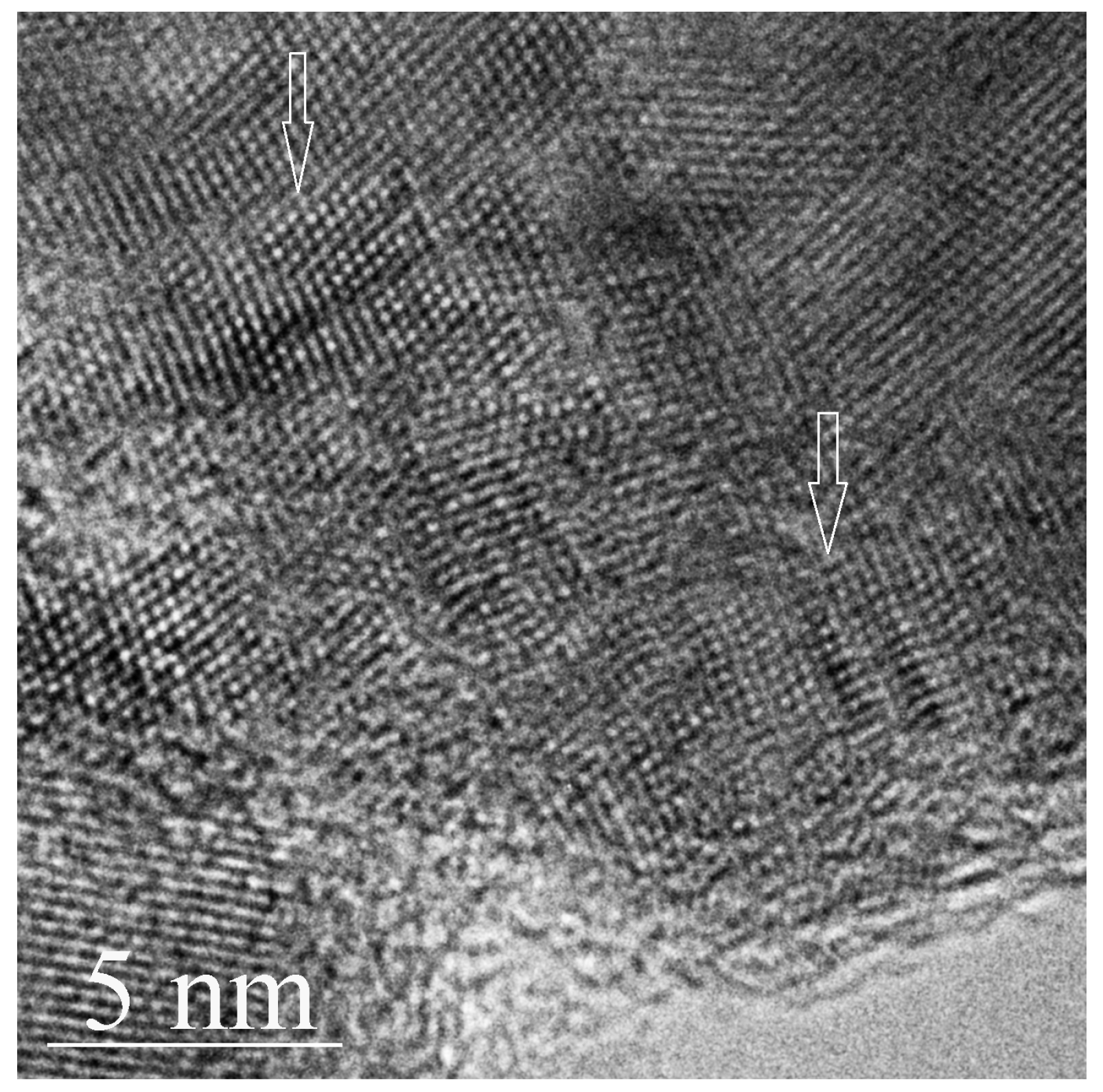
3. Results
4. Discussion
5. Conclusions
Author Contributions
Acknowledgments
Conflicts of Interest
References
- He, J.; Chung, K.H.; Liao, X.; Zhu, Y.T.; Laverna, E.J. Mechanical milling-induced deformation twinning in fcc materials with high stacking fault energy. Metall. Mater. Trans. A 2003, 34, 707–712. [Google Scholar] [CrossRef]
- Klassen, T.; Oehring, M.; Bormann, R. Microscopic mechanisms of metastable phase formation during ball milling of intermetallic TiAl phases. Acta Mater. 1997, 45, 3935–3948. [Google Scholar] [CrossRef]
- Kulnitskiy, B.; Annenkov, M.; Perezhogin, I.; Popov, M.; Ovsyannikov, D.; Blank, V. Mutual transformation between crystalline phases in silicon after treatment in a planetary mill: HRTEM studies. Acta Crystallogr. 2016, B72, 733–737. [Google Scholar] [CrossRef] [PubMed]
- Sides, C.R.; Li, N.C.; Patrissi, C.J.; Scrosati, B.; Martin, C.R. Nanoscale Materials for Lithium-Ion Batteries. MRS Bull. 2002, 27, 604–607. [Google Scholar] [CrossRef]
- Tang, J.; Wang, H.; Lee, D.H.; Fardy, M.; Huo, Z.; Russell, T.P.; Yang, P. Holey Silicon as an Efficient Thermoelectric Material. Nano Lett. 2010, 10, 4279–4283. [Google Scholar] [CrossRef] [PubMed] [Green Version]
- Ovsyannikov, D.A.; Popov, M.Y.; Buga, S.G.; Kirichenko, A.N.; Tarelkin, S.A.; Aksenenkov, V.V.; Tat’yanin, E.V.; Blank, V.D. Transport Properties of Nanocomposite Thermoelectric Materials Based on Si and Ge. Phys. Solid State 2015, 57, 605–612. [Google Scholar] [CrossRef]
- Popov, M.; Buga, S.; Vysikaylo, P.; Stepanov, P.; Skok, V.; Medvedev, V.; Tatyanin, E.; Denisov, V.; Kirichenko, A.; Aksenenkov, V.; et al. C60-doping of nanostructured Bi–Sb–Tethermoelectrics. Phys. Status Solidi A 2011, 208, 2783–2789. [Google Scholar] [CrossRef]
- George, A. Properties of Crystalline Silicon; Hull, R., Ed.; INSPEC, the Institution of Electrical Engineers: London, UK, 1999; pp. 104–107. ISBN 159124871X 9781591248712 0852969333 9780852969335. [Google Scholar]
- Wentorf, R.H.; Kasper, J.S. Two New Forms of Silicon. Science 1963, 139, 338–339. [Google Scholar] [CrossRef]
- Kasper, J.S.; Richards, S.M. The Crystal Structures of New Forms of Silicon and Germanium. Acta Crystallogr. 1964, 17, 752–755. [Google Scholar] [CrossRef]
- Eremenko, G.; Nikitenko, I. Electron-microscope investigation of microplastic deformation mechanisms of silicon by indentation. Phys. Status Solidi A 1972, 14, 317–330. [Google Scholar] [CrossRef]
- Zhang, X.; Zhao, L.D. Thermoelectric materials: Energy conversion between heat and electricity. J. Mater. 2015, 1, 92–105. [Google Scholar] [CrossRef]
- Annenkov, M.; Blank, V.; Kulnitskiy, B.; Larionov, K.; Ovsyannikov, D.; Perezhogin, I.; Popov, M.; Sorokin, P. Boron carbide nanoparticles for high-hardness ceramics: Crystallattice defects after treatment in a planetary ball mill. J. Eur. Ceram. Soc. 2017, 37, 1349–1353. [Google Scholar] [CrossRef]
- Sahibzada, S.R.; Wei, J.; Shahzad, A.K.; Fun, Z.; Zhang, F. Microstructure and mechanical properties of B4C densified by spark plasma sintering with Si as a sintering aid. Ceram. Int. 2015, 41, 1903–1906. [Google Scholar] [CrossRef]
- Blank, V.D.; Kulnitskiy, B.A. Crystallogeometry of polymorphic transitions in silicon under prtessure. High Press Res. 1996, 15, 31–42. [Google Scholar] [CrossRef]
- Blank, V.D.; Estrin, E.I. Phase Transitions in Solids under High Pressure; CRC Press (Taylor and Francis Group): Boca Raton, FL, USA, 2014; p. 441. ISBN 978-1-4665-9424-1. [Google Scholar]
- Takacs, L.; McHenry, J.S. Temperature of the milling balls in shaker and planetary mills. J. Mater. Sci. 2006, 41, 5246–5249. [Google Scholar] [CrossRef]
- Veliotti, J.B.; Pan, X.; Ma, X. New Research on Solid State Chemistry; Veliotti, J.B., Ed.; Nova Science Publishers: Hauppauge, NY, USA, 2007; pp. 157–181. ISBN 10 1-60021-264-6. [Google Scholar]
- Maurice, D.R.; Courtney, T.H. The physics of mechanical alloying: A first report. Metall. Mater. Trans. A 1990, 21, 289–303. [Google Scholar] [CrossRef]
- Domnich, V.; Gogotsi, Y.; Trenary, M.; Tanaka, T. Nanoindentation and Raman spectroscopy studies of boron carbide single crystals. Rev. Adv. Mater. Sci. 2002, 3, 3783. [Google Scholar] [CrossRef]
- Fissel, A.; Bugiel, E.; Wang, C.R.; Osten, H.J. Formation of twinning-superlattice regions by artificial stacking of Si layers. J. Cryst. Growth 2006, 290, 392–397. [Google Scholar] [CrossRef]
- Mylvaganam, K.; Zhang, L.C. Nanotwinning in monocrystalline silicon upon nanoscratching. Scr. Mater. 2011, 65, 214–216. [Google Scholar] [CrossRef]


© 2018 by the authors. Licensee MDPI, Basel, Switzerland. This article is an open access article distributed under the terms and conditions of the Creative Commons Attribution (CC BY) license (http://creativecommons.org/licenses/by/4.0/).
Share and Cite
Kulnitskiy, B.A.; Perezhogin, I.A.; Popov, M.Y.; Ovsyannikov, D.A.; Blank, V.D. Peculiarities of the Twinning in Silicon during Ball Milling in the Presence of Two Different Materials. Symmetry 2018, 10, 200. https://doi.org/10.3390/sym10060200
Kulnitskiy BA, Perezhogin IA, Popov MY, Ovsyannikov DA, Blank VD. Peculiarities of the Twinning in Silicon during Ball Milling in the Presence of Two Different Materials. Symmetry. 2018; 10(6):200. https://doi.org/10.3390/sym10060200
Chicago/Turabian StyleKulnitskiy, Boris A., Igor A. Perezhogin, Mikhail Yu. Popov, Danila A. Ovsyannikov, and Vladimir D. Blank. 2018. "Peculiarities of the Twinning in Silicon during Ball Milling in the Presence of Two Different Materials" Symmetry 10, no. 6: 200. https://doi.org/10.3390/sym10060200