1. Introduction
Recently, electronic films and packaging substrate structures in electronic devices have been developed to be thinner and smaller than ever before [
1,
2,
3]. To meet the current trend of electronic packaging devices, inevitably, the warpage problem has become a critical issue, which occurs from the residual stress accumulated from various fabrication and assembly processes [
4,
5], asymmetric design, and complex material used in the thin film structures for multifunction and high performance in electronics. The warpage problem induces fatal interconnection defects and initiates the weak connection between silicon chips and printed-circuit-board (PCB) by causing the misalignment, non-wet and contact area decrease when silicon chip is mounted on the packaging board [
6,
7]. Also, the vertical warping and curling of structures in the surface micromachining leads to degradation of functionality of micro-devices [
8]. Therefore, a systematic basic study of the warpage of packaging substrate is necessary in order to analyze the warpage behavior mechanism and solve the warpage issues.
Kim
et al., investigated warpage mechanism of strip panel type plastic ball grid array (PBFA) package. The effect on warpage of cure shrinkage, thermo-mechanical properties of the molding compound substrates, and package geometry are characterized [
9]. Chou
et al., reviewed several analytic solutions including Suhir’s formula, Stoney’ equation, and extend Stoney’s equation, to validate the applicability of residual stress estimation of film-substrate structures. They conducted finite element method (FEM) simulation and compared the result with the different solutions, emphasizing the residual stress induced by the coefficient of thermal expansion (CTE) mismatch as a major cause of mechanical failures in integrated circuits or electronic packages [
10]. Zhu
et al., identified warpage origination due to CTE mismatch between composing materials during wafer level packaging processes [
11]. Likewise, there have been many other studies on thermally induced warpage [
12,
13,
14].
For polymer-based substrates, however, residual stress in Cu film after electroplating can be another major factor, which affects the warpage. Although the built-in stress of electroplated Cu has been actively researched [
15,
16,
17], no previous studies have focused on the residual stress after electroplating of Cu as a major warpage factor. When it is combined with compliant and thin polymer composite substrate, the residual stress itself causes warpage in effect. In this study, we propose a new method for warpage analysis and investigate the importance of considering the initial residual stress of Cu film layer.
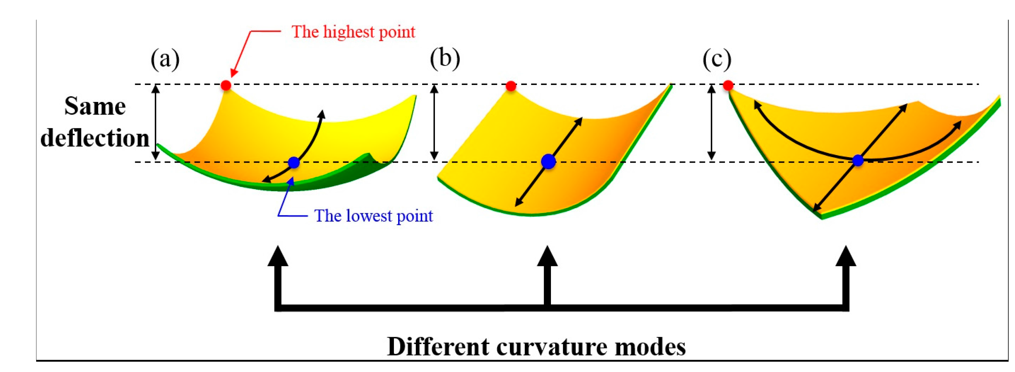
In previous studies, the distance between the highest and lowest points is typically used as the quantitative value of warpage [
18,
19,
20,
21]. However, the maximum deflection measurement has several limitations, including the boundary effects and the specimen size dependence. Moreover, the maximum deflection measurement does not completely represent the overall deformation shape of the specimen. For instance, as shown in
Figure 1, although all the specimens have the same deflection, curvature modes and magnitude are different, respectively.
Figure 1a shows a spherical shape, which has same curvature in all directions.
Figure 1b,c show two cylindrical shapes with different curvature orientation. The specimen curvatures include the information of the entire deformation shape as well as the specimen deflections, and therefore the curvature measurement can be a key method to quantitatively investigate the warpage.
Figure 1.
Typical warpage modes of square shape specimens: (a) spherical shape; (b) cylindrical shape; and (c) cylindrical diagonal shape.
Figure 1.
Typical warpage modes of square shape specimens: (a) spherical shape; (b) cylindrical shape; and (c) cylindrical diagonal shape.
Another advantage of the curvature measurement is the calculation of the built-in stress of a deposited thin film. The residual stress of thin films can be measured from other methods, such as X-ray diffraction [
22,
23], nano-indentation [
24,
25,
26], and digital image correlation after focused ion beam milling [
27,
28]. Compared to these methods, the curvature measurement method is not limited to local area depending on the tip size or the machine size, obtaining effective residual stress in non-destructive manner. In addition, the stress measurement from the curvature does not require cumbersome preprocesses such as surface polishing and cutting for specimen fabrication.
Many of the previous studies on measuring built-in stress in film layer utilized Stoney’s equation, which is applicable for small edge deflections with spherical shape. The small warpage of metal on glass, ceramic on silicon wafer structures can be well predicted by the analytic solution with the non-contact method. However, as the glass fiber-reinforced polymer (GFRP) substrates are much compliant and thinner compared to the conventional substrates, larger deformation should be analyzed. To analyze the non-linear, large out-of-plane deformation, Suo model was properly adopted in this study [
29].
In this paper, a warpage analysis method consisting of four procedures (
Figure 2) for electroplated Cu films on fiber-reinforced polymer (FRP) packaging substrates was developed. The warpage analysis sequence is as follows: specimen preparation, 3D surface scanning of the specimens and curvature fitting, calculation of the built-in film stress, and warpage prediction via the FEM simulation and verification of results through comparisons with the measured data. The warpage behavior of the bilayer specimens was observed at room temperature and also throughout the reflow process temperature range between 25 and 180 °C (
Figure 2a). The optical 3D scanner was used to measure the precise shapes of the specimens at room temperature and also during heating and cooling (
Figure 2b). The built-in stress of the film layers was calculated using the specimen’s curvature, which was extracted from the captured data using polynomial 3D curve fitting, from the analytic model (
Figure 2c). The warpage was predicted for whole temperature range using FEM simulation and the simulation results were compared with measured data to verify the accuracy of simulation model (
Figure 2d). In the FEM method, the built-in stress calculated from the curvature measurement is directly applied to the simulation modeling and also the thermal stress is considered. In summary, the warpage analysis method is presented to find a new factor that affects the warpage at room temperature and to predict warpage behavior at a wide range of temperature.
Figure 2.
Warpage analysis procedure: (a) The bilayer specimen with the size of 44 × 56 mm is prepared which is bent due to residual stress at room temperature; (b) Shape measurement by non-contact 3D scanner; (c) Curvature fitting for calculation of the residual stress; (d) FEM simulation result of the room temperature warpage. Both experimental result and simulation result are compared each other.
2. Methodology of Warpage Analysis
2.1. Warpage Analysis Procedure
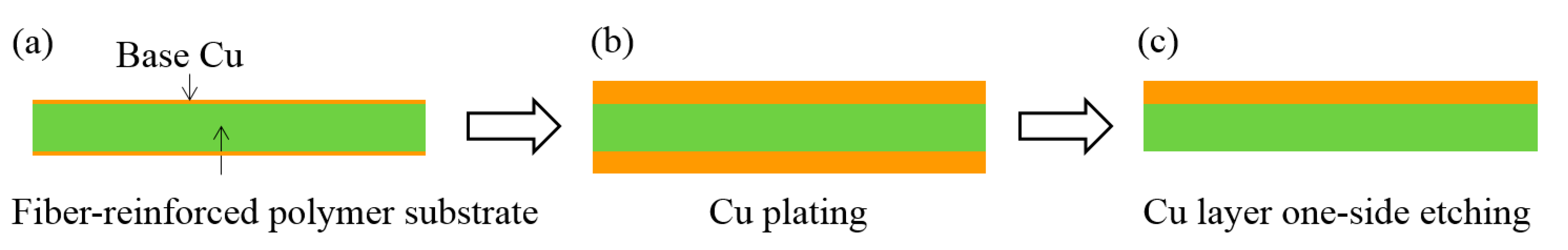
First of all, the bilayer test specimens were fabricated by layering a Cu film on a FRP substrate.
Figure 3 illustrates the specimen preparation sequence. The base Cu was laminated on both sides of the substrate, which is a thin layer of approximately 1 μm for Cu electrochemical plating (
Figure 3a). The Cu film with a thickness of 5~20 μm was electroplated; the thickness was controlled using the electric current density, ASD (ampere per square decimeter). Both sides of the specimen were electroplated symmetrically while passing through plating bath (
Figure 3b). When one side of the Cu specimen was etched out, the specimen became an asymmetric structure (
Figure 3c) and deformed into a curved shape due to the plating stress of the Cu layer. Consequently, curved bilayer structure with one-sided Cu film on the FRP substrate is prepared.
Figure 3.
Bilayer specimen producing process: (a) fiber-reinforced polymer substrate with two base Cu with thickness of 1 μm; (b) electrochemical Cu plating with thickness of 5~20 μm symmetrically on the base Cu; and (c) one side Cu etch down.
Figure 3.
Bilayer specimen producing process: (a) fiber-reinforced polymer substrate with two base Cu with thickness of 1 μm; (b) electrochemical Cu plating with thickness of 5~20 μm symmetrically on the base Cu; and (c) one side Cu etch down.
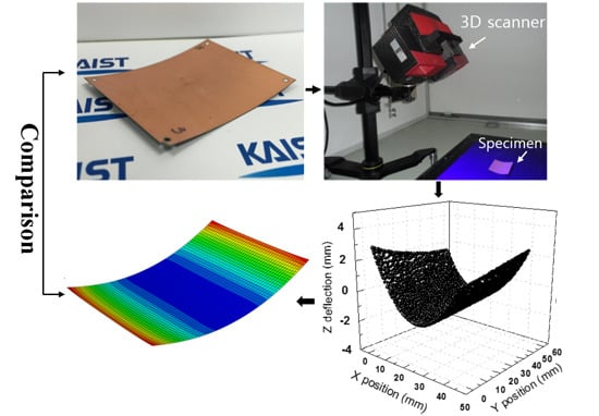
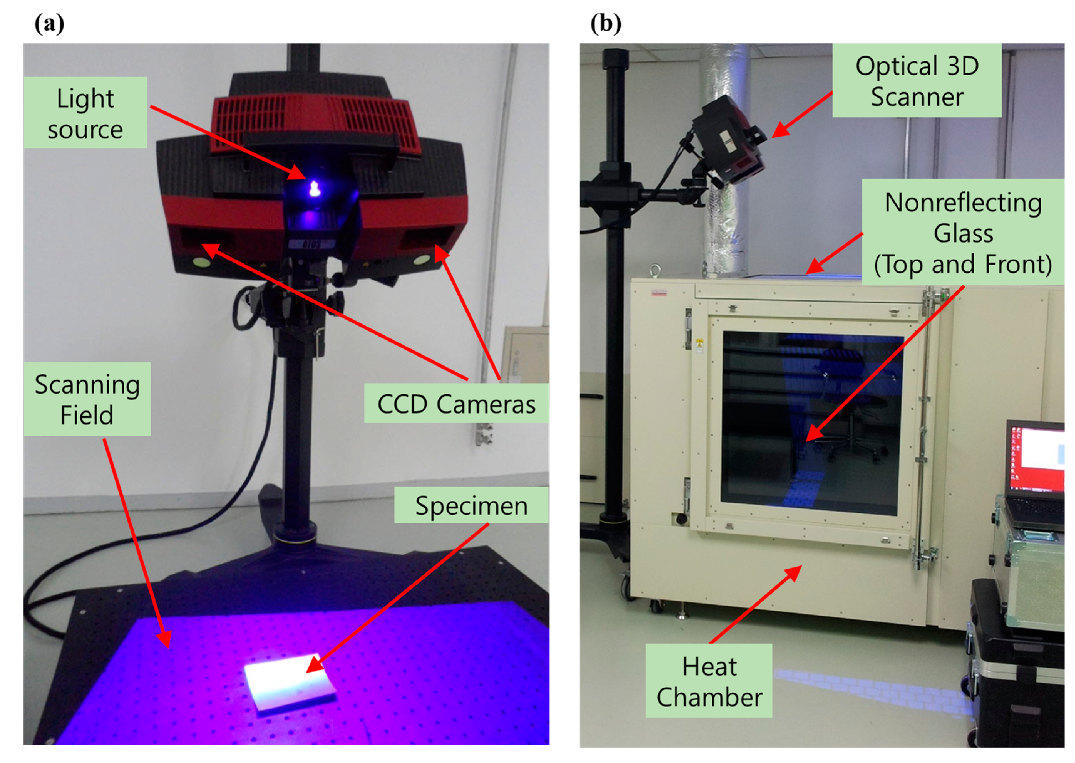
Next step is specimens’ contour measurement. The specimen contours were measured using an optical 3D scanner (ATOS, GOM mbH, Braunschweig, Germany) as illustrated in
Figure 4. The 3D scanner system is based on projection moiré topography method, in which the grating or interference fringes are projected onto the surface of specimen. Two charged coupled device (CCD) cameras simultaneously capture the blue interference fringe pattern, which are spread from the light source, onto the surface of each specimen (
Figure 4a). The 3D scanner is able to get clear images regardless of the brightness of specimen’s surface and to deal with multiple specimens at once if specimens are within the field of view. Since the projection moiré doesn’t require pre-processing of spray coating on the specimen, it allows in-line measurement during subsequent clean processes such as circuit patterning and film lamination. On the other hand, because conventional imaging technics such as shadow moiré fails to capture image of shiny specimens, artificial spray coating is mandatory to remove surface glaring. Accordingly, the shadow moiré cannot be used for capturing the images of the specimens in the post processes due to risk of contamination. In addition, another major benefit is the rapidity of data processing, allowing the geometry of specimens to be captured in 6–8 s. Even if the specimen experiences large deformation, the optical 3D scanner captures it without noise or an out focusing problem.
For thermal warpage behavior analysis, the specimens were placed in the heating chamber and heated up to 180 °C in order to measure the images during the temperature change (
Figure 4b). The non-reflective top and front windows were mounted on the heating chamber for the purpose of capturing the clear image of specimens by preventing unwanted reflected light pattern into cameras. A thermocouple was attached on a dummy sample in order to confirm the temperature of specimen inside of the heating chamber. The deformed contours were measured
in situ at pre-defined temperatures during the heating and cooling steps.
Figure 4.
(a) Specimen contour measurement using an optical 3D scanner; and (b) In situ measurement using a heating chamber with nonreflecting glass.
Figure 4.
(a) Specimen contour measurement using an optical 3D scanner; and (b) In situ measurement using a heating chamber with nonreflecting glass.
The deformed contours measured by the optical 3D scanner include a set of points and vectors with three-dimensional coordinate values. These contours were fitted to the second order of the polynomial equation to calculate curvatures. For deformed surfaces where the squares of the slopes are small compared with the unity, the curvature of each axis is defined as follows:
where
w = f(
x,
y) is a specimen contour that indicates the measured deflection from the flat plane state.
kx and
ky are the curvatures along two directions mutually orthogonal to
x and
y, respectively.
kxy and
kyx define the diagonal curvatures, which are the rate of change in the slope perpendicular to the direction of travel. Due to the symmetry of the curvature tensor,
kxy and
kyx are theoretically the same. The principal curvatures can be obtained using the coordinate transformation and removal of
kxy, as follows:
where
k1 is the principal maximum curvature and
k2 is the principal minimum curvature. The obtained curvatures were substituted into the analytic model in order to calculate the built-in stress along the in-plane directions.
Lastly, in order to verify the experimental results, FEM simulations was performed. ABAQUS v 6.12-1 (Dassault Systèmes, Vélizy-Villacoublay, France) was used as the simulation tool. The curvature of the simulation results with that of the experiment results were compared during the temperature change. The built-in stress of the film layer was directly defined into the deposited film in the simulation model in order to obtain accurate results of warpage simulation.
2.2. Built-In Stress Calculation from Curvature-Stress Relationship
For a quantitative analysis of warpage, it is necessary to calculate the built-in stress of the film layer, because the warpage behavior without a thermal process depends on the built-in stress caused by the deposition process at room temperature. Stress measurement of thin film based on curvature has been developed from the Stoney’s equation for various applications [
30]. Stoney’s equation is well known as the most common approach for obtaining the built-in stress of thin film from the curvature. The curvature of Stoney’s equation with the stress in the thin films is given as follows:
where σ
f is the biaxial stress,
hf and
hs are the film thickness and substrate thickness, respectively, and
Es′ is the plane strain modulus of substrate,
Es/(1 −
vs). However, this model is applicable in limited cases. It is valid only when the substrate and film have uniform thickness, the properties of substrate are linear elastic and isotropic, the out-of-plane displacement should be at least an order of magnitude less than the substrate thickness, and system should behave within the linear range. The curvature proportionally increases with maintaining the spherical shape within the linear range when the built-in stress of film increases. However, once the film strain becomes large and overcomes the linear range, it changes its shape into a cylindrical shape, which has one dominant curved orientation. This phenomenon is called curvature bifurcation and should be considered for precise warpage analysis. Therefore, Stoney’s equation is not directly applicable to certain cases where the substrate is relatively compliant and the film is highly deformed within the nonlinear range.
Many researchers have presented models for predicting geometrically nonlinear stress-curvature relations [
31,
32,
33,
34,
35,
36,
37,
38]. Suo
et al. [
29] has derived a model for nonlinearly behaving bilayer structures. Their analytic model is applicable when the substrate is compliant and the film is stiffer than the substrate. The equation that was used in this study considers the mechanical properties of film and the substrate, while Stoney’s equation only considered the properties of substrate. In addition, it is valid for very large deformation that causes the curvature bifurcation. The relationship between the radius of the curvature (a reciprocal of curvature) and the strain is as follows [
39]:
with
where, R is the radius of the specimen curvature of the cylindrical shape after the bifurcation occurs and (
ef −
es) is the mismatch strain between the film and the substrate.
E′,
h, and
v are the plane strain modulus, thickness, and Poisson ratio, respectively. The subscripts
f and
s indicate the film and substrate, respectively.
The mismatch strain is generated by the difference in non-mechanical strain of each layer. In our study, the non-mechanical strain is composed of two components: The thermal mismatch strain is caused by the CTE mismatch during the temperature change. The built-in strain is induced in the film during the deposition process. The non-mechanical strain of film and substrate are defined as follows:
Hence the mismatch strain is:
where α is the coefficient of thermal expansion, T
d is deposition temperature, T
r is room temperature and
εbi is the built-in strain of the deposited film resulting from grain growth. Because the Cu electroplating is conducted at room temperature in plating bath, (
ef −
es) in Equation (6c) becomes equal to
εbi.
Now the built-in strain of film can be determined from the Equation (5), since all other variables are known: The material properties of film and substrate are measured, and the radius of curvature can be calculated from the contour of out-of-plane deflection. Therefore, the residual built-in stress of Cu film is calculated using the product of the plane strain modulus and built-in strain of film, as described in the following equation:
2.3. Material Property Measurement
2.3.1. Flexural Modulus Measurement
Fiber-reinforced polymer (FRP) substrates are polymer-based composites with bundles of glass fibers and widely used in the electronic industry. In this research, cross-woven fiber-reinforced polymer substrate, which composed of bundles of individual filaments that were orthogonally woven together to create a glass fabric, was used. The orthotropic properties of the FRP substrate were attributed to the structure of the orthogonally woven glass fabric. The warp and weft directions are two directions of fiber, which are usually woven orthogonally. The warp is the longitudinal direction where the fibers are under tension that originates from the roll-to-roll process used in fabricating the composite and the weft is the transverse direction drawn through the warp direction. Due to this directionality of material, the properties such as Young’s modulus of the composite depend on the fiber orientation. Therefore, the material properties along fiber directions are required for accurate warpage prediction.
To properly analyze the bending behavior of the polymer composite laminates, the flexural modulus of the FRP substrates was measured by three-point bending test. For the thin and stiff GFRP substrate (0.1–0.16 mm), tensile test machine has problems such as gripping and pulling the thin film. However, grips are not required in the three-point bending test; it is possible to eliminate the slippage problem in advance. For the three-point bending test, the FRP substrate specimens were cut from the raw sheet in rectangular pieces with a dimension of 5 × 20 mm. Following the American Society for Testing and Materials (ASTM) standards, specific conditions are determined [
40,
41]. The sample is placed on the support with a span length of 9mm. The loading nose with a tip radius of 0.5 mm travels down for 0.4 mm and returns to the initial position, with a speed of 12 μm/s. The tests were conducted from 25 to 180 °C, at every interval of 30 °C.
2.3.2. Shear Modulus Calculation
The orthotropic materials have principal material axes: transverse and longitudinal directions, which are the warp and weft direction in the FRP substrate, respectively. The transformation to the arbitrary direction of the engineering constants are related to the four independent engineering constants (
EL,
ET,
vLT,
GLT) as seen in the following equations [
42,
43]:
Because it is difficult to measure the shear modulus of the FRP composite directly, we prepared the specimens that were cut in directions of 0°, 45° and 90°.
EL,
ET and
Eθ were measured using the three-point bending test, and
was given by the manufacturer. When θ is 45°, the shear modulus (
GLT) is formulated as follows:
2.3.3. Coefficient of Thermal Expansion Measurement
Coefficient of thermal expansion was measured by a thermo-mechanical analyzer (TMA 402 F1, Netzsch, Selb/Bavaria, Germany). Sample size was 8 mm in width and 30 mm for the gage length of film tension mode. Temperature increased from 25 to 180 °C with a heating rate of 4 °C/min. CTE value was measured in warp direction and confirmed to be constant throughout the heating range.
2.4. Warpage Simulation Model
The FEM simulation was performed in order to verify the experimental results. In the previous studies, it was difficult to predict the warpage at the room and high temperature. Because the previous simulation assumed that the warpage was zero at the deposition temperature and only the thermal stress caused by CTE misfit was considered for the factor of warpage. In order to obtain the room temperature warpage, the temperature was lowered from the deposition temperature to room temperature. However, in case of electroplating process, which is performed at room temperature, it is difficult to obtain the room temperature warpage.
ABAQUS v 6.12-1 was used as the simulation tool. The geometry is drawn in a 2D shell model; the mesh element was an S4R shell composite. For accurate observation of the overall warpage behavior, a full model was drawn instead of a quarter model. In the property module, Cu film was on the top of the FRP substrate and orientations of both materials were set as 0°. Three section points were used for integration points per one layer. Regarding the mechanical boundary conditions, displacements and rotations along the three axes are restricted at the center of the specimen model.
To verify the importance the initial built-in stress in Cu film layer, the warpage values obtained from both with and without built-in stress are compared with experimental results. The FEM analysis with built-in stress was conducted in 2 separate steps. Step 1 was room temperature warpage due to built-in stress after Cu electroplating. The built-in stress calculated from the curvature method is applied to Cu film in the first step. ABAQUS/CAE (Complete Abaqus Environment) provides initial stress input as predefined field at the node set or element set. However, shell model shares its nodes and elements with all layers; it is not possible to apply the built-in stress to the film section only. Thus input file, which contains the simulation information, was edited, and SECTION POINTS command was added into the history command to separately apply the predefined-stress field. Tensile stress of Cu film induces the specimen warp in convex shape and curvature is obtained for the validation. The initial thermal conditions for the entire layers were set to an ambient temperature of 25 °C. The following step is a thermal cycle, which predicts the curvature in the higher temperature. The temperature was increased to 180 °C and decreased to initial temperature throughout the modeling region.
The simulation without built-in stress assumed that both room temperature and high temperature warpage are occurred solely by CTE mismatch. From the experiment, the temperature when the specimen is flat, where the curvature is zero, can be found. Without built-in stress simulation is enacted by the method which is frequently used to predict the room temperature warpage of packaging substrate by cooling from the warpage free temperature to room temperature [
44,
45]. For example, it is 8 and 90 °C for
Figure 6a,b, respectively. The specimen is assumed to be stress free at the temperatures. Accordingly, the initial simulation step started at the temperatures. Now the step 1 induces room temperature warpage by decreasing the temperature field to 25 °C. After obtaining the room temperature warpage, the temperature filed is increased to 180 °C and decreased to 25 °C again as well.
3. Results and Discussion
The specimens were prepared in order to calculate the built-in stress of the Cu film layer and measure the warpage behavior during the temperature change. The Cu layer was deposited on the FRP substrate with a panel size of 405 × 510 mm. The Cu layer thickness was controlled using the electric current density and plating time. The Cu-plated FRP of panel was sliced into 64 specimens with the size of 44 × 56 mm for one specimen. Among the 64 specimens, three specimens were selected for the thermal process. Two specimens were located along the edge of the panel and one was in the middle of the panel. After the electroplating and routing processes, the specimens were placed in the heating chamber. One dummy specimen was also put inside the heating chamber with a thermocouple in order to read the temperature of the specimen. When the dummy thermocouple indicated the temperature at which one want to measure, the 3D scanner captured the contours of all specimens immediately. The highest temperature of thermal process was 180 °C, which is same temperature of reflow process. For this research, two types of commercialized FRP packaging substrates with different thicknesses and mechanical properties were used: the type A FRP substrate was thinner and more compliant than the type B FRP substrate. The thickness type A FRP substrate has 100 μm and that of type B FRP substrate is 150 μm. Cu films of 9 μm and 17 μm thickness were electroplated on the both types of FRP substrates. The flexural moduli along the 0°, 45°, and 90° and detail material properties are presented in
Table 1. Regarding the temperature dependence, the moduli decrease linearly with increasing temperature, and therefore only maximum and minimum values are reported in
Table 1. The measured values at each temperature were applied in the FEM analysis with linear interpolation in the temperature ranges where no data is available. For the material properties of copper layer, isotropic modulus of 105 GPa, Poisson’s ratio of 0.34, and CTE value of 18.0 ppm/°C were used [
46].
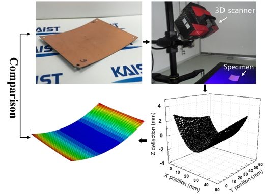
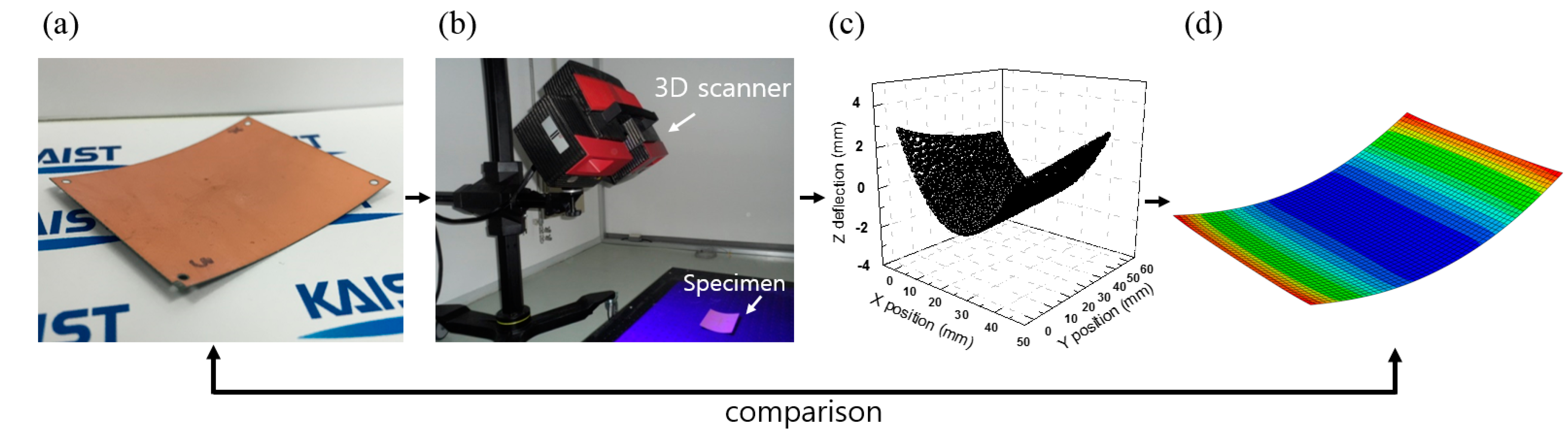
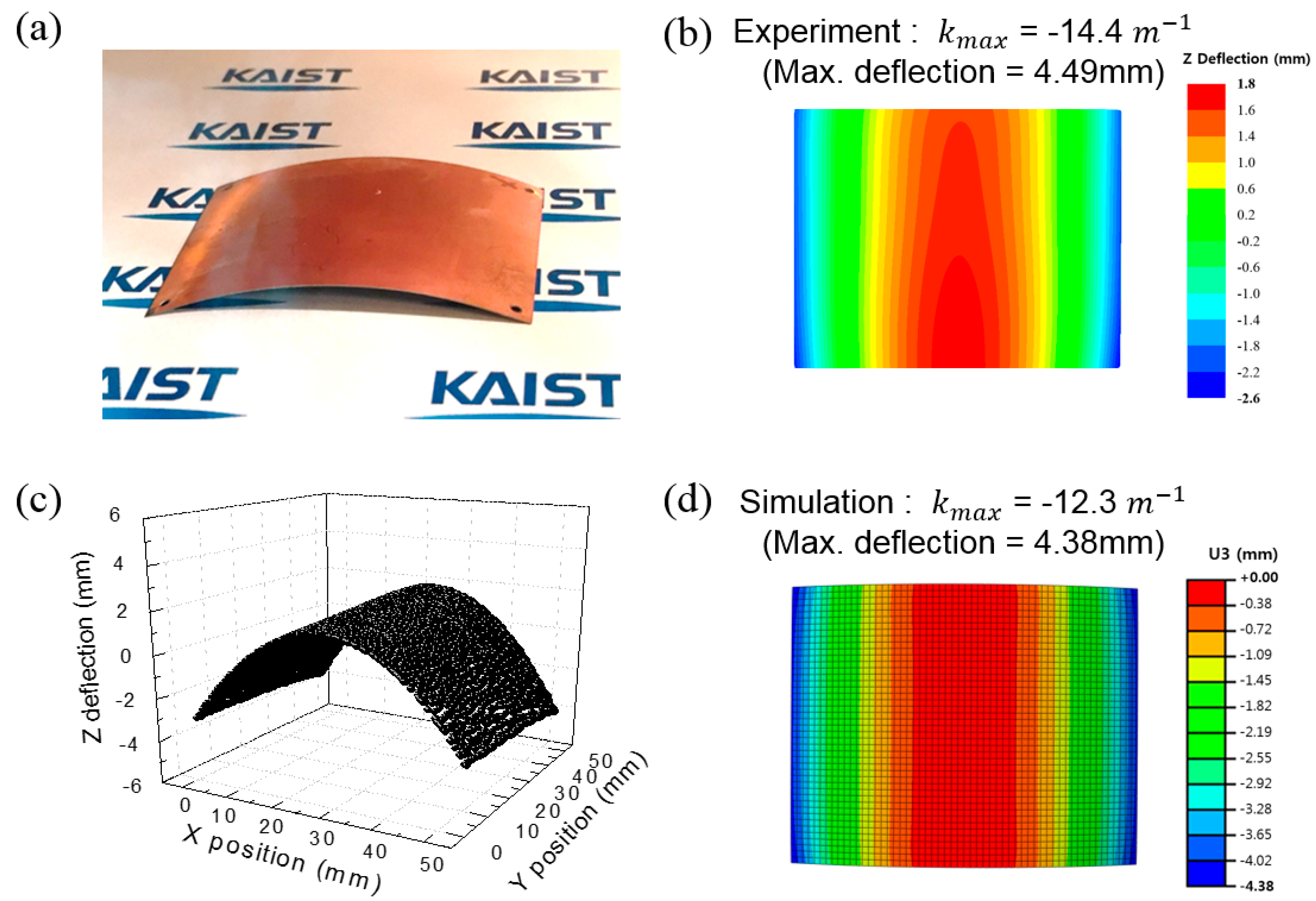
Figure 5 presents the contour of experimental and simulation result of the type A FRP specimen with 17 μm Cu film at 180 °C.
Figure 5a shows specimen in the heating chamber.
Figure 5b is top view image of the specimen measured by optical 3D scanner. The 3D scanner saved the data, which contains location information of fringe pattern reflected on the specimen’s surface and automatically showed the contour with legend.
Figure 5c is 3D curve fitting for calculating curvatures of specimen. The data is plotted using OriginPro 8 (OriginLab Corporation, Northampton, MA, USA). Each point in the
Figure 5c has three-dimensional coordinate values.
Figure 5d is the side view of the simulation result. Both experiment and simulation result show cylindrical shape.
Table 1.
Measured flexural moduli along the longitudinal, transversal and 45° directions, calculated shear moduli, coefficient of thermal expansion (CTE) and glass transition temperature of type A and B fiber-reinforced polymers (FRPs) at 25 and 180 °C. Poisson’s ratio and glass transition temperature were provided by manufacturer’s data table.
| Substrate Type | EL (GPa) | ET (GPa) | E45° (GPa) | VLT | GLT (GPa) | CTE (ppm/°C) | Tg (°C) |
|---|
| Type A FRP | At 25°C | 14.26 ± 0.15 | 14.18 ± 0.56 | 13.11 ± 0.22 | 0.2 | 5.19 | 7.95 | 230 |
| At 180°C | 12.68 ± 0.25 | 12.47 ± 0.34 | 11.09 ± 0.20 | 0.2 | 4.29 |
| Type B FRP | At 25°C | 25.13 ± 0.13 | 26.65 ± 0.12 | 24.63 ± 0.05 | 0.2 | 9.93 | 7.09 | 225 |
| At 180°C | 19.72 ± 0.18 | 22.41 ± 0.22 | 19.85 ± 0.24 | 0.2 | 7.91 |
Figure 5.
Type A FRP specimen with 17 μm Cu film at 180 °C: (a) specimen in the heating chamber; (b) contour measured by 3D scanner (top view); (c) 3D curve fitting done by data analysis program; and (d) the simulation result (top view).
Figure 5.
Type A FRP specimen with 17 μm Cu film at 180 °C: (a) specimen in the heating chamber; (b) contour measured by 3D scanner (top view); (c) 3D curve fitting done by data analysis program; and (d) the simulation result (top view).
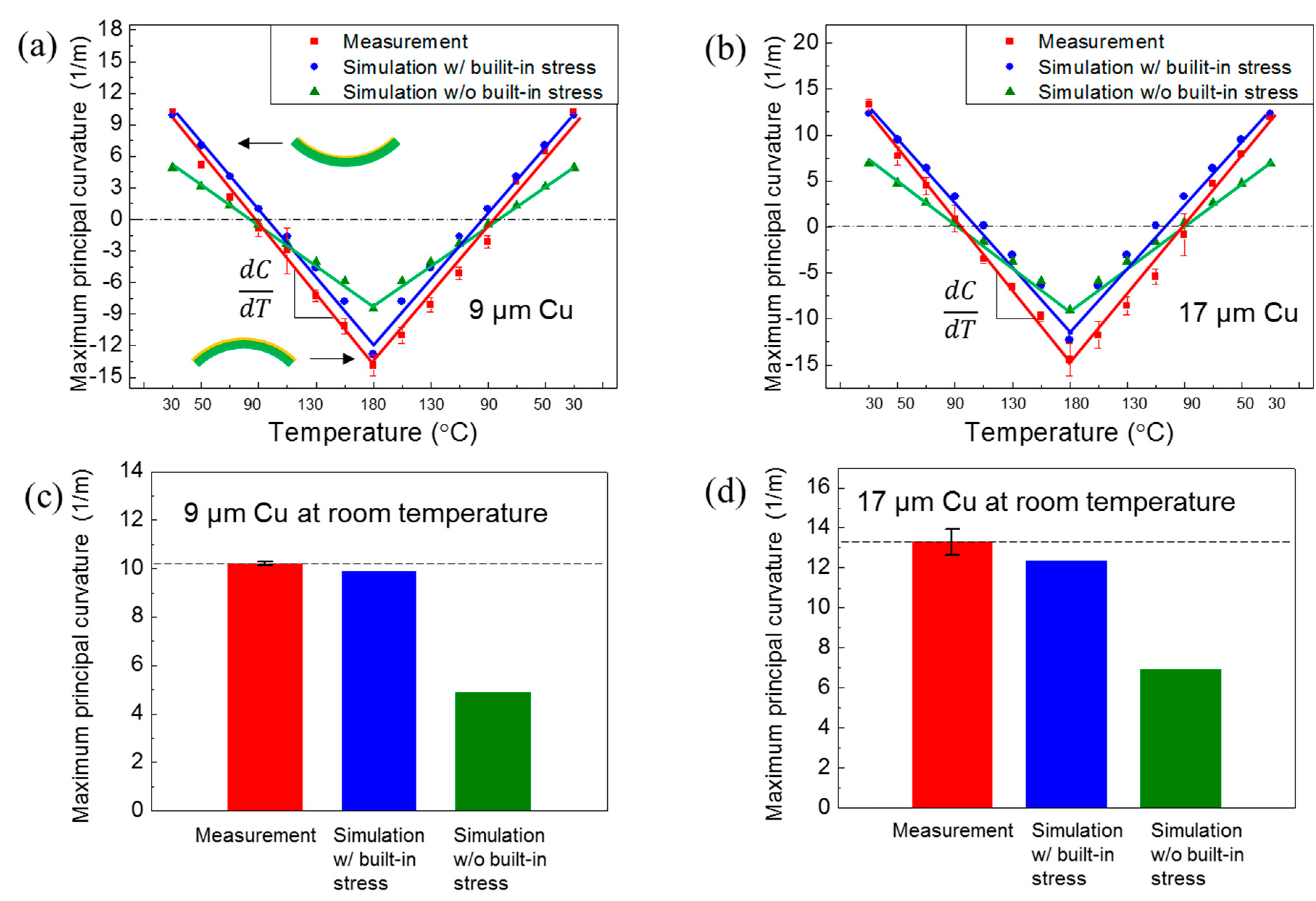
We compared the maximum principal curvature of the experimental measurement and two FEM simulation results. Two parameters were used for the curvature comparison to quantify the accuracy of warpage simulation. The simulation accuracy (%) is the first parameter, which is defined as ksimulation/kmeasurement × 100. This parameter is for quantification of accuracy at the particular temperature. Second parameter is dC/dT (m−1∙°C−1), which represents the rate of curvature change with respect to temperature. This parameter, slope of the curvature versus temperature, is able to compare the curvature of measurement and simulation results in the whole temperature.
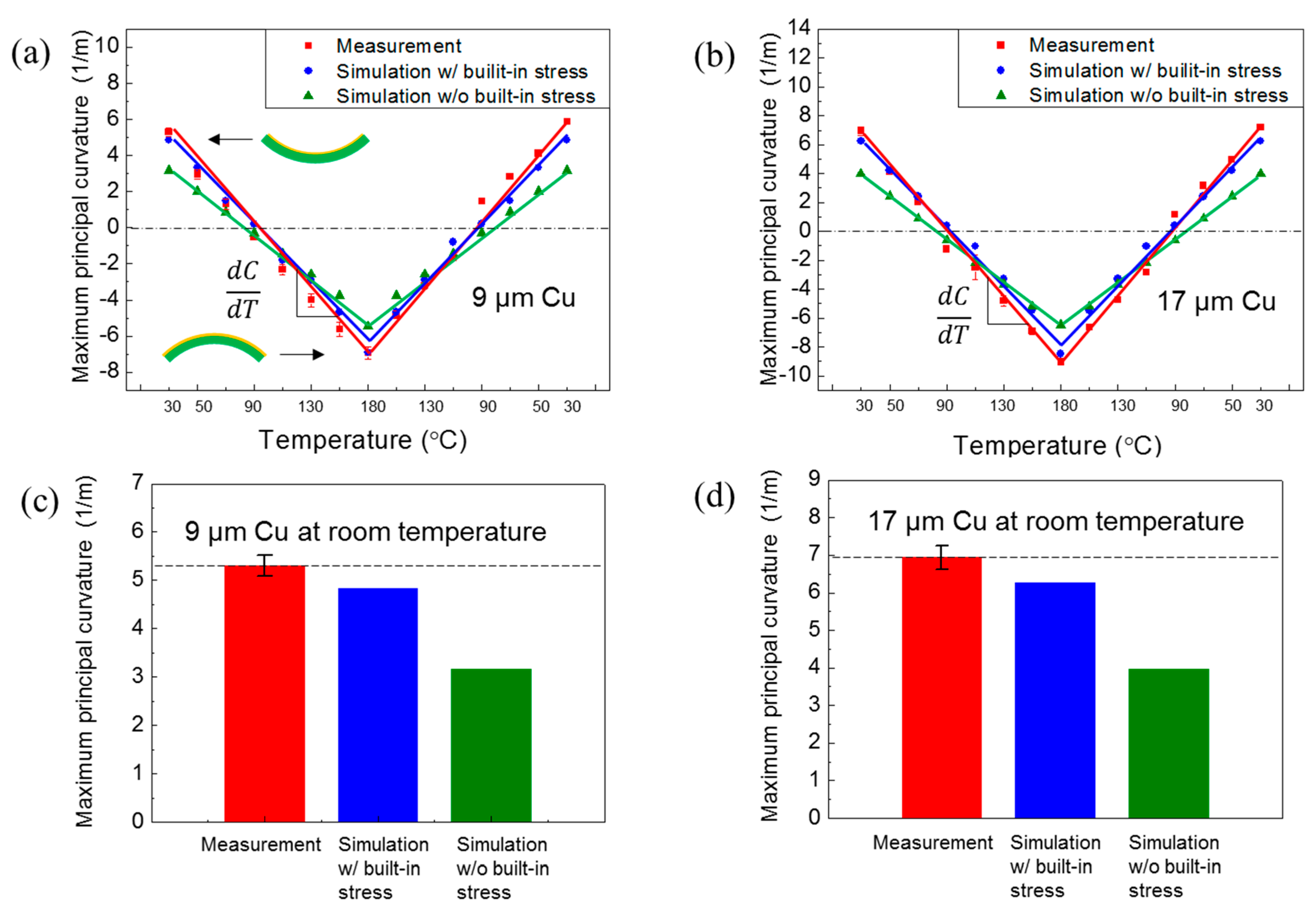
The curvature comparisons among the experimental measurement and two simulation results of the specimens of type A FRP substrate are plotted in
Figure 6. Specimens of experiment and simulation modeling maintain cylindrical shape in the range from 25 to 80 °C and changed from convex to concave near the 90 °C. At this transition temperature, the mode of curvature changes from convex to concave. This is an unstable point; therefore, the specimen is deformed into the saddle shape where both positive and negative curvatures are present in a specimen. In this case, the larger curvature is chosen for the curvature comparison. Warpage mode is changed from concave to convex at the transition temperature and the curvatures of convex specimen increase above the transition temperature. When the temperature was increased continuously, Cu layer expands more than FRP substrate because FRP substrate has smaller CTE than Cu film. Therefore, as the temperature increases, the curvatures of concave specimen decrease.
Curvature of specimens with the 9 μm (
Figure 6a) and 17 μm (
Figure 6b) thickness Cu films were measured at room temperature and observed during the temperature change in the heating chamber. The curvatures of the simulation with built-in stress aligned with the measured results for the whole region, whereas the curvature of simulation without built-in stress was smaller than that of the measured data, especially at room temperature and the highest temperature. The maximum principal curvatures of experimental measurement and two simulations at the room temperature are presented in
Figure 6c,d. The simulations with built-in stress and without built-in stress were compared with measured data. The simulation accuracy of simulation with built-in stress with 9 μm Cu specimen at room temperature is 96.6%, while that of simulation without built-in stress is 48%. Similarly, for the case of 17 μm Cu specimen, the simulation accuracies of simulation with and without built-in stress at room temperature show 93% and 51.9%, respectively. The simulation with built-in stress is more accurate than simulation without built-in stress. The simulation without built-in stress is far below the measured data.
Table 2 presents the rate of curvature change with respect to temperature of measurement result and simulation with and without built-in stress about type A FRP with 9 μm and 17 μm Cu film. The values of
dC/
dT in the
Table 2 are the absolute value, because curvature value could be positive or negative depending on the position of specimen (positive sign for convex, negative sign for concave). The simulation was performed in the elastic range, therefore the rate of curvature change with respect to temperature at the heating and cooling are identical. The
dC/
dT of measurement of type A FRP with 9 μm Cu film at the heating is 0.1568 m
−1∙°C
−1, while that of simulation with and without built-in stress is 0.1696 and 0.0919 m
−1∙°C
−1, respectively. The result of simulation with built-in stress is well matched with measurement date. However, the
dC/
dT of simulation without built-in stress is far below compared with measurement data. Although the value of
dC/
dT in the cooling is slightly higher compared with the value of heating due to experimental noise, the
dC/
dT of measurement and simulation with built-in stress also show a similar value. For the case of 17 µm Cu film, the
dC/
dT of the simulation without built-in stress is almost half of the measurement value.
Figure 6.
Maximum principal curvature comparison of type A FRP specimens among experimental measurement, simulation results with and without built-in stress: (a) type A specimens with 9 μm Cu; (b) type A specimens with 17 μm Cu, and maximum principal curvature at room temperature with (c) 9 μm Cu and (d) 17 μm Cu films.
Table 2.
The comparison of the dC/dT values for measurement, simulation with and without built in stress of type A FRP substrates.
Table 2.
The comparison of the dC/dT values for measurement, simulation with and without built in stress of type A FRP substrates.
| Thickness of Cu on Type A FRP (μm) | Measurement (m−1∙°C−1) | Simulation with Built-in Stress (m−1∙°C−1) | Simulation without Built-in Stress (m−1∙°C−1) |
|---|
| 9 | 0.1568 (Heating) | 0.1696 | 0.0919 |
| 0.1666 (Cooling) |
| 17 | 0.1756 (Heating) | 0.1630 | 0.1061 |
| 0.1882 (Cooling) |
The curvature comparisons of the specimens of type B FRP substrate are plotted in
Figure 7.
Figure 7a,b represent curvatures of the 9 μm and 17 μm Cu specimens, respectively, during the temperature change. The results from type B FRP substrate with two different Cu thicknesses are similar to that of type A FRP substrate. The curvatures of the simulation with built-in stress well match with the measured results for the entire temperature range.
Figure 7c,d show the maximum principal curvatures of experimental measurement and two simulations with the 9 μm (
Figure 7c) and 17 μm (
Figure 7d) films, respectively, at room temperature. Also, similar to the A FRP case, the simulation result with built-in stress also showed higher accuracy. The measured curvatures of both types of 17 μm Cu film specimens at room temperature were higher than that of 9 μm Cu film specimens. The experimental measurement and proposed simulation results of both FRP specimens exhibited over 90% accuracy at room temperature curvature. For the case of 9 μm Cu specimen, the simulation accuracies of simulation with and without built-in stress at room temperature are 91.8% and 59.8%, respectively. Similarly, for the case of 17 μm Cu specimen, the simulation accuracies of simulation with and without built-in stress at room temperature are 90.2% and 46.4%, respectively. The comparison also exhibited good agreement with the measured curvature and simulation results over the entire temperature region. However, the simulation results without built-in stress were not matched with the actual measurement. Therefore, it is clear that the built-in stress is required for accurate warpage prediction.
Figure 7.
Maximum principal curvature comparison of type B FRP specimens among experimental measurement, simulation results with and without built-in stress: (a) type B specimens with 9 μm Cu; (b) type B specimens with 17 μm Cu; and maximum principal curvature at room temperature with (c) 9 μm Cu and (d) 17 μm Cu films.
Table 3 presents the rate of curvature change with respect to temperature of measurement result and simulation with and without built-in stress about type B FRP with 9 μm and 17 μm Cu film. Although the values of the
dC/
dT are small compared to the values of type A FRP specimens, the overall tendency is the same regardless of Cu thickness and substrate type. The simulation with built-in stress accurately corresponds to the measurement compared to the simulation without built-in stress. Therefore, simulation with built-in stress is able to precisely predict warpage behavior of electroplated Cu films on FRP packaging substrates.
Table 3.
The comparison of the dC/dT values for measurement, simulation with and without built in stress of type B FRP substrates.
Table 3.
The comparison of the dC/dT values for measurement, simulation with and without built in stress of type B FRP substrates.
| Thickness of Cu on Type B FRP (μm) | Measurement (m−1∙°C−1) | Simulation with Built-in Stress (m−1∙°C−1) | Simulation without Built-in Stress (m−1∙°C−1) |
|---|
| 9 | 0.0832 (Heating) | 0.0795 | 0.0577 |
| 0.0887 (Cooling) |
| 17 | 0.1073 (Heating) | 0.0986 | 0.0721 |
| 0.1135 (Cooling) |
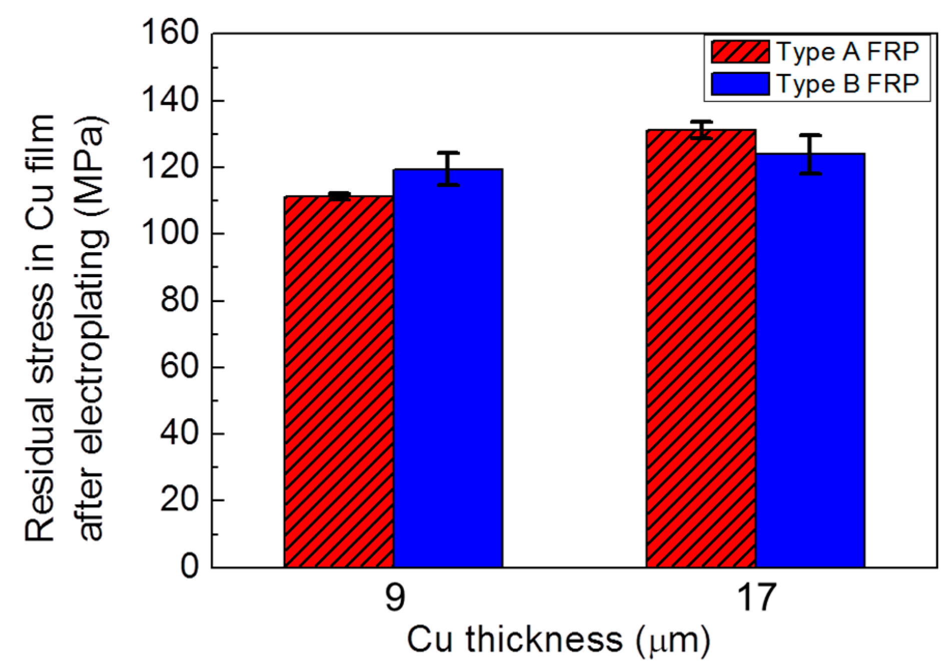
The built-in stresses of each specimen were quantitatively calculated from the curvatures. The built-in stress was induced when the film layers were deposited on the substrate. The Cu films were electroplated on the base Cu attached to the FRP packaging substrate, and this process caused the electroplating stress in the Cu film.
Figure 8 illustrates the electroplating stresses along the Cu thickness and type of substrate. The built-in stress (electroplating stress) of type A FRP with 9 μm is 111.2 MPa and it increase to 131.2 MPa with 19 μm thickness of Cu film. In the case of type B FRP, the built-in stress with 9 μm is 119.5 MPa and 123.9 MPa for 19 μm. Although the built-in stress of Cu film on the type A FRP substrate slightly increased as the Cu thickness increased, the built-in stress of Cu film on the type B FRP substrate presents almost the same value. This is a higher value than previous studies, which is previously measured from a silicon substrate specimen [
15,
16,
17]. The yield strength of electroplated Cu film is in the range of 250~450 MPa in the previous literatures [
47,
48,
49]. Therefore, it is confirmed that the residual stress of Cu films is in linear elastic range.
Figure 8.
Comparison of residual stress in Cu film after electroplating of type A and B FRP specimens with 9 and 17 μm Cu films.
Figure 8.
Comparison of residual stress in Cu film after electroplating of type A and B FRP specimens with 9 and 17 μm Cu films.
To sum up, the residual stress in Cu film on different substrates is measured to reproduce and predict the warpage at room temperature. Our modeling approach should rely on the resultant curvature of the specimen at room temperature, which requires experimental verification for accurate prediction of each substrate. Once the results are accumulated as a database, the method is useful in industrial applications, such as criteria of substrate selection or structural decision-making.


