Article

Photo-Crosslinking of Pendent Uracil Units Provides Supramolecular Hole Injection/Transport Conducting Polymers for Highly Efficient Light-Emitting Diodes

1
Institute of Applied Chemistry, National Chiao Tung University, HsinChu, 30010, Taiwan
2
Graduate Institute of Applied Science and Technology, National Taiwan University of Science and Technology, Taipei City 10607, Taiwan
3
Department of Materials and Optoelectronic Science, National Sun Yat-Sen University, Kaohsiung 80424, Taiwan
*
Authors to whom correspondence should be addressed.
Polymers 2015, 7(5), 804-818; https://doi.org/10.3390/polym7050804
Submission received: 27 March 2015 / Revised: 16 April 2015 / Accepted: 22 April 2015 / Published: 27 April 2015

Abstract

:
A new process for modifying a polymeric material for use as a hole injection transport layer in organic light-emitting diodes has been studied, which is through 2π + 2π photodimerization of a DNA-mimetic π-conjugated poly(triphenylamine-carbazole) presenting pendent uracil groups (PTC-U) under 1 h of UV irradiation. Multilayer florescence OLED (Organic light-emitting diodes) device with the PTC-U-1hr as a hole injection/transport layer (ITO (Indium tin oxide)/HITL (hole-injection/transport layer) (15 nm)/N,N'-di(1-naphthyl)-N,N'-diphenyl-(1,1'-biphenyl)-4,4'-diamine (NPB) (15 nm)/Tris-(8-hydroxyquinoline)aluminum (Alq3) (60 nm)/LiF (1 nm)/Al (100 nm)) is fabricated, a remarkable improvement in performance (Qmax (external quantum efficiency) = 2.65%, Bmax (maximum brightness) = 56,704 cd/m2, and LE (luminance efficiency)max = 8.9 cd/A) relative to the control PTC-U (Qmax = 2.40%, Bmax = 40,490 cd/m2, and LEmax = 8.0 cd/A). Multilayer phosphorescence OLED device with the PTC-U-1hr as a hole injection/transport layer (ITO/HITL (15 nm)/Ir(ppy)3:PVK (40 nm)/BCP (10nm)/Alq3 (40 nm)/LiF (1 nm)/Al (100 nm)) is fabricated by successive spin-coating processes, a remarkable improvement in performance (Qmax = 9.68%, Bmax = 41,466 cd/m2, and LEmax = 36.6 cd/A) relative to the control PTC-U (Qmax = 8.35%, Bmax = 34,978 cd/m2, and LEmax = 30.8 cd/A) and the commercial product (poly(3,4-ethylenedioxythiophene):polystyrenesulfonate) PEDOT:PSS (Qmax = 4.29%, Bmax = 15,678 cd/m2, and LEmax = 16.2 cd/A) has been achieved.

Graphical Abstract

1. Introduction

Organic light-emitting diodes (OLEDs) and polymer light-emitting diodes (PLEDs) are among the most promising technologies for use in next-generation light sources and flat-panel displays, because they can be prepared over large areas with light weights and can be operated with rapid responses, low power consumption, and wide viewing angles [1,2,3,4]. High-efficiency LED devices typically feature one or more organic layers—namely, the hole-injection/transport layer (HITL), the electron-emitting layer (EML), and/or the electron-injection/transport layer (EITL)—sandwiched between the two electrodes. The limiting factors in determining the operating voltage, luminance efficiency (LE), external quantum efficiency (EQE), and brightness are the degrees of charge injection and transport. Charge injection and transport from both the anode and cathode must be balanced to recombine in the electron-emitting layer to enhance the efficiency and performance of OLED devices [5,6]. Therefore, HITLs play an important role in OLEDs because they allow enhanced hole injection from the indium tin oxide (ITO) anode into the EML, resulting in balanced charge injection/transport and better performance [7].
Hole injection/transport materials (HITMs) deposited through solution processing are typically based on poly(3,4-ethylenedioxythiophene):polystyrenesulfonate (PEDOT:PSS), which has good hole injection ability, high conductivity (1–10 S/m), and reasonable ionization potential (Ip = −5.2 eV) [8,9]. Indeed, deposition of polymers from organic solvents onto PEDOT:PSS, which is itself typically deposited from aqueous solution and insoluble in organic solvents, is a common process during device fabrication [10]. Nevertheless, PEDOT:PSS is a strongly acidic polymer that can degrade a device and emittor, thereby limiting its lifetime [11,12]. PEDOT:PSS is fabricated from a water dispersion, which is also relatively more damaging for OLED devices than neutral conjugated polymers [13]. Therefore, efforts to develop new HITMs, including neither hydrophilic nor ionic functionalities, yet exhibiting excellent resistance toward organic solvents, have also been pursued actively. Conjugated polymers that have crosslinked network structures typically exhibit higher hole mobilities and solvent resistance properties because of the electronic communication between the polymer chains [14,15]. Jen et al. [16,17] synthesized a series of di(styrene)-functionalized triphenylamine derivatives that were crosslinkable hole transporting layer (HTL) materials. Crosslinked di(styrene)-functionalized triphenylamine derivatives can be placed, through solution processing, between the PEDOT:PSS layer and the emission layer to improve the efficiency of OLED devices. Hole injection-transporting materials (HITMs) having crosslinked network structures display solvent resistance, thereby avoiding interfacial mixing during the solution processing through spin-coating—an important factor toward achieving highly efficient OLED devices [18,19,20,21,22,23,24,25].
In previous studies, we found that the multiple hydrogen bonding interactions of nucleobase-functionalized polymers can result in physically crosslinked structures having substantially increased glass transition temperatures (Tg) [26]. Furthermore, we developed a new DNA-mimetic π-conjugated poly(triphenylamine-carbazole) presenting pendent uracil (U) moieties (PTC-U) that exhibited high thermal stability and excellent hole injection and good electron-blocking ability in the solid state, due to physical crosslinking of the U units [27]. Furthermore, a trilayer device incorporating PTC-U as the HITL displayed a maximum brightness as high as 48,233 cd/m2, an EQE of 2.40%, and an LE of 8.0 cd/A, values that are comparable with those reported (efficiency: 1.70 or 1.08 cd/A; maximum brightness: 7500 cd/m2) for a corresponding device featuring conventional PEDOT:PSS as the HITL [28,29]. Nevertheless, the HITL of PTC-U was slightly destroyed upon exposure to the solution containing the emitting layer during subsequent spin-coating. Because U is a photoactive pyrimidine base that can undergo 2π + 2π photodimerization [29,30,31], in this study we investigated a new method for solution processing of PTC-U based on 2π + 2π photodimerization to increase its solvent resistance and thermal stability (Figures S1 and S2).

2. Experimental Section
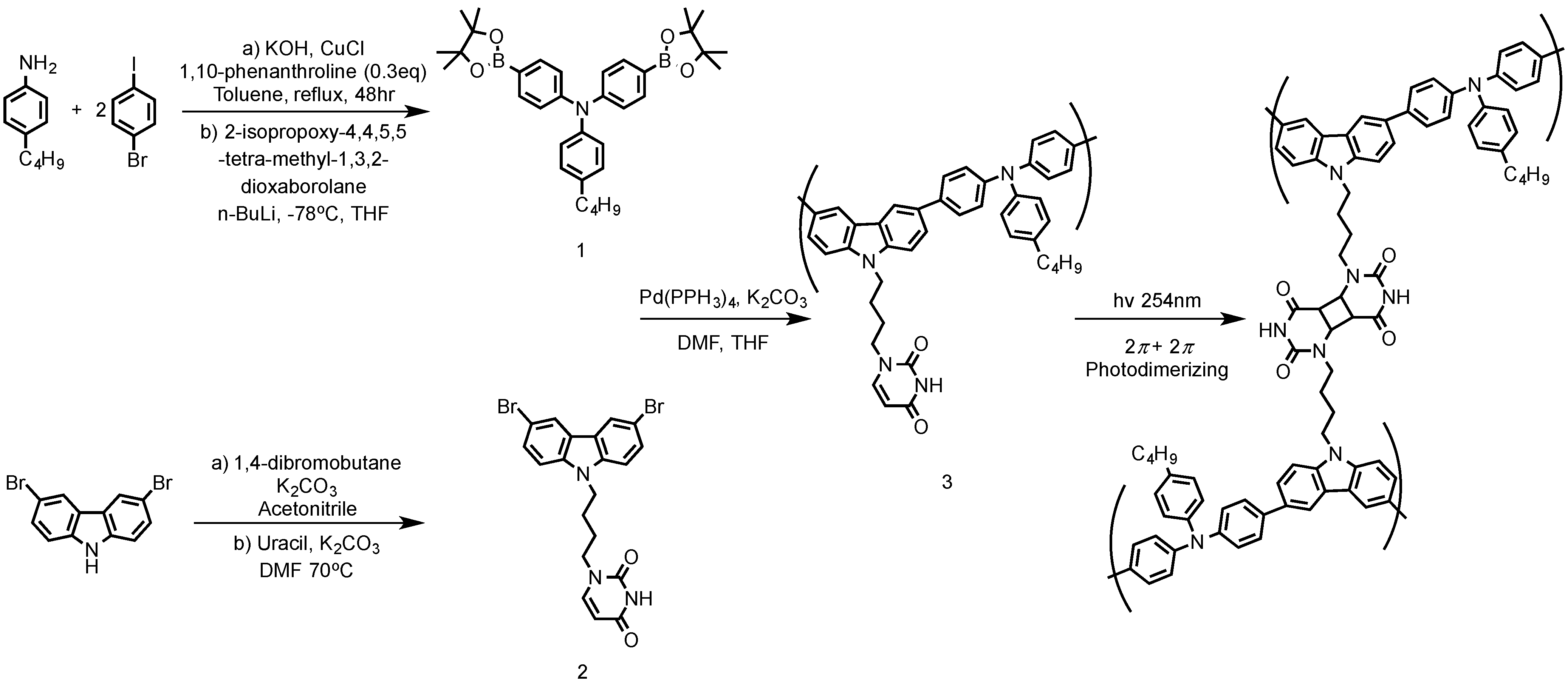
2.1. Materials

All reagents were obtained from Sigma-Aldrich (St. Louis, MO, USA) and Acros Organic (St. Louis, MO, USA) and used as received. All solvents were purchased from TEDIA (Fairfield, OH, USA) and distilled over CaH2 prior to use. 4-butyl-N,N-bis(4-bromophenyl)aniline, 4-butyl-N,N-bis(4,4,5,5-tetramethyl-1,3,2-dioxaborolane-4-phenyl)aniline (1), 4-bromobutyl-9-(3,6-dibromocarbazole) (2), and PTC-U (3) were synthesized according to the procedures reported previously [27]. A solution of PTC-U (1 wt% in 1,1,2,2-tetrachloroethane) was spin-coated (2000 rpm, 30 s) onto ITO glass. The spin-coated film was irradiated at short wavelength (254 nm) in the presence of an ultraviolet crosslinker (UVP CL-1000, Upland, CA, USA).

2.2. Characterization

UV-Vis spectra were recorded using an HP 8453 diode-array spectrophotometer (Santa Clara, CA, USA). PL (photoluminescence) spectra were recorded using a Hitachi F4500 luminescence spectrometer (Schaumburg, IL, USA). Cyclic voltammetry (CV) was performed using a BAS 100 B/W electrochemical analyzer (West Lafayette, IN, USA) operated at a scan rate of 100 mV/s; the potentials were measured against a Ag/Ag+ (0.01 M AgNO3) reference electrode using ferrocene/ferrocenium (Fc/Fc+) as the internal standard. Atomic force microscope (AFM), equipped with a Hitachi High-Tech Instrument Scanning Probe Microscope (AFM5300E) and dynamic force mode, was used to examine surface morphology and to estimate thickness and root-mean-square (RMS) roughness of deposited films. FTIR (Fourier transform infrared spectroscopy) spectra of the polymer films were recorded using a Bruker Tensor27 FTIR spectrophotometer (El Monte, CA, USA) and the conventional KBr disk method; 32 scans were collected at a spectral resolution of 4 cm−1.

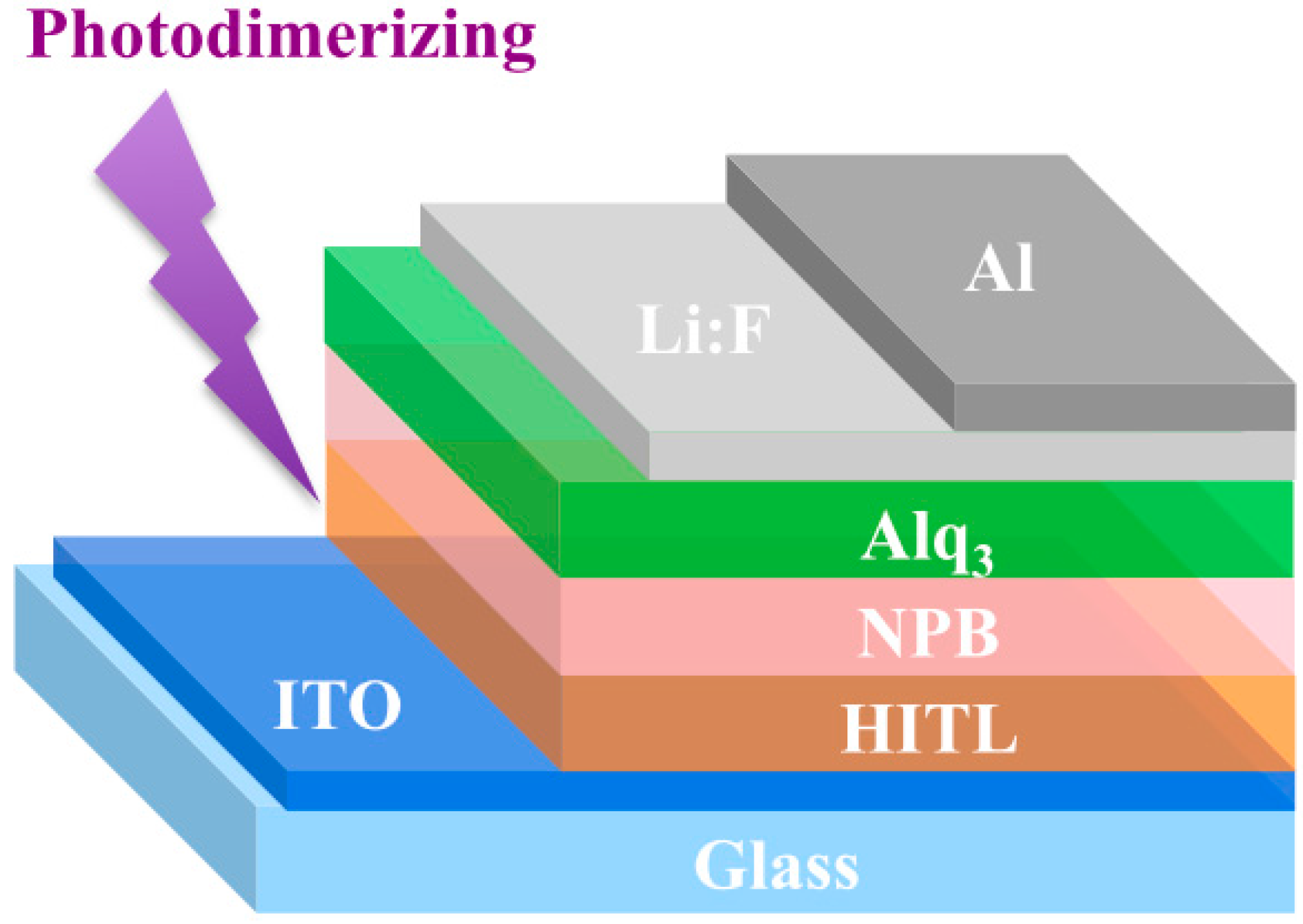
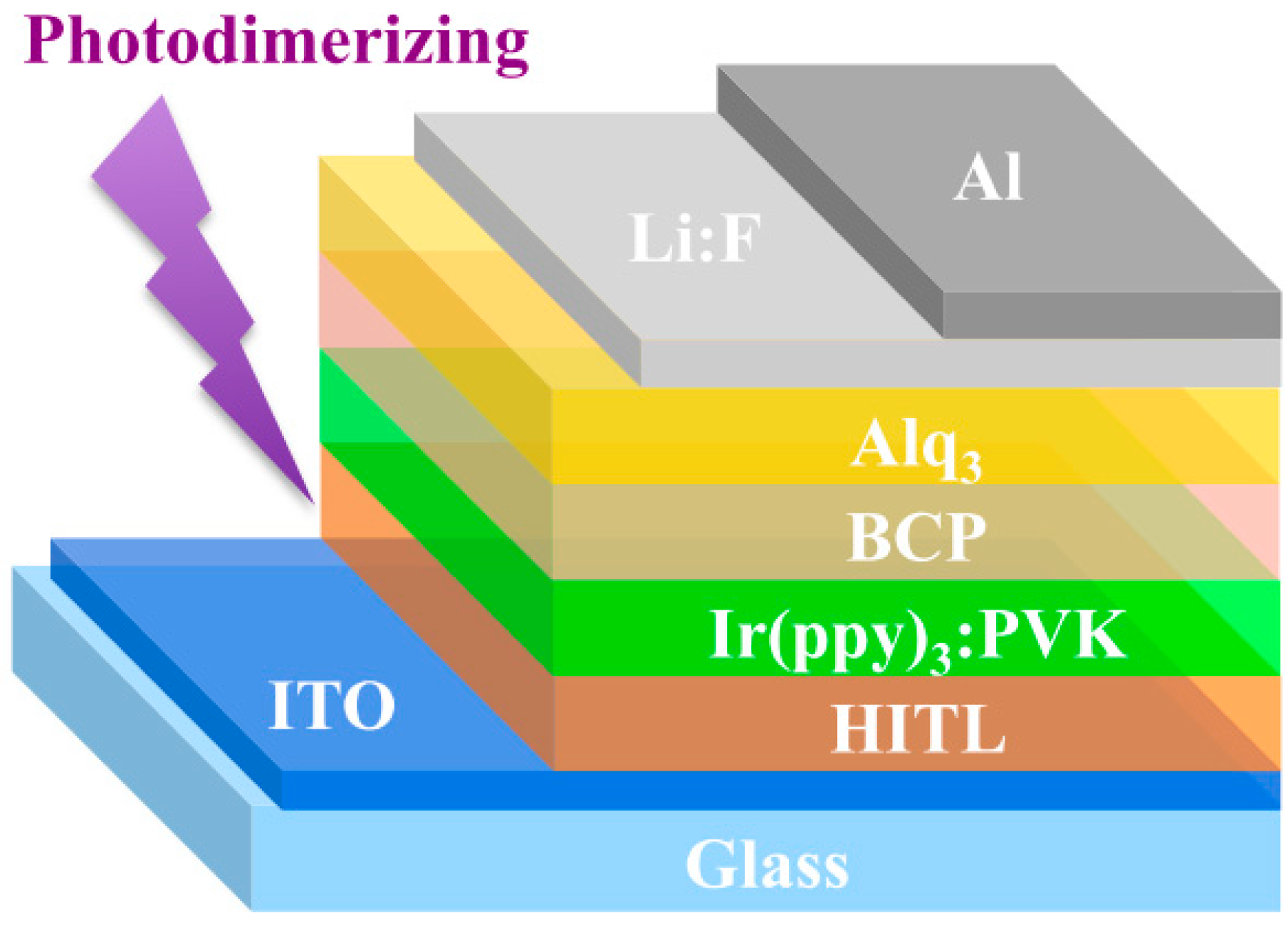
2.3. Fabrication of OLEDs

The HITL materials deposited by spin coating (15 nm) onto a UV-ozone cleaned ITO glass with a sheet resistance of 25 Ω·square−1, and the other EL devices were fabricated by vacuum deposition of the materials at 10−6 torr sequentially. The deposited at a rate of all the small molecular organic layers (BCP, NPB, and Alq3) were 1.0 Å·s−1. The cathode was completed through thermal deposition of LiF at a deposition rate of 0.1 Å·s−1, then capped with Al metal through evaporation at rate of 4.0 Å·s−1. The deposited thickness are: NPB (15 nm), Alq3 (60 nm), LiF (1 nm), Al (100 nm) for florescence OLED device, and BCP (10 nm), Alq3 (40 nm), LiF (1 nm), and Al (100 nm) for phosphorescence OLED device. The relationship of the current density and brightness of the devices with respect to voltage were measured using a Keithley 2400 source meter (Moorpark, CA, USA) and a Newport 1835C optical meter (Lake Mary, FL, USA) equipped with an 818ST silicon photodiode. The EL spectrum was obtained using a Hitachi F4500 luminescence spectrometer. The emissive layer was formed via spin-coating a blend solution of poly(vinylcarbazole) (PVK) and fac-tri(2-phenylprydine) iridium(III) (Ir(ppy)3) in chlorobenzene (total 1.5 wt% in chlorobenzene, 6 wt% Ir(ppy)3:PVK). The device based on PEDOT:PSS (Bayer, Baytron P VP AI 4083, Sheffield, UK) was fabricated as the control device. All OLED devices tested at least 3 times for each types of device, and the standard deviation is less than 10% of these efficiency values.

3. Results and Discussion

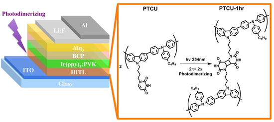
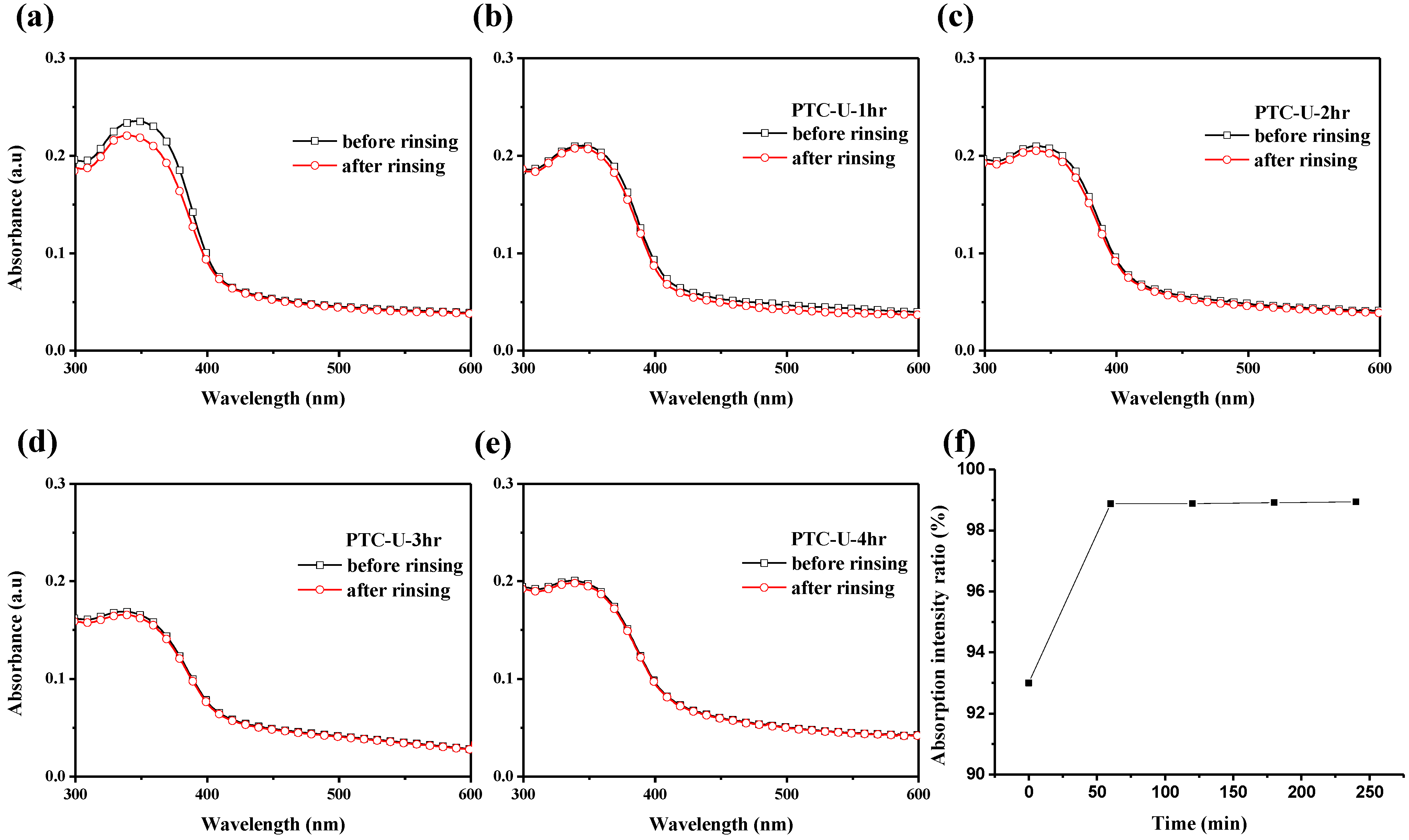
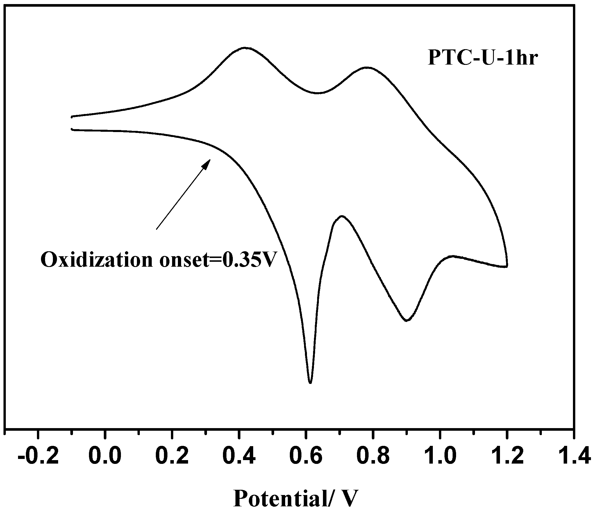
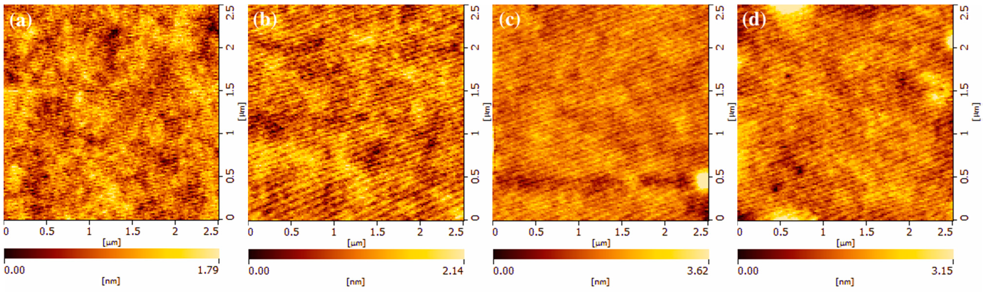
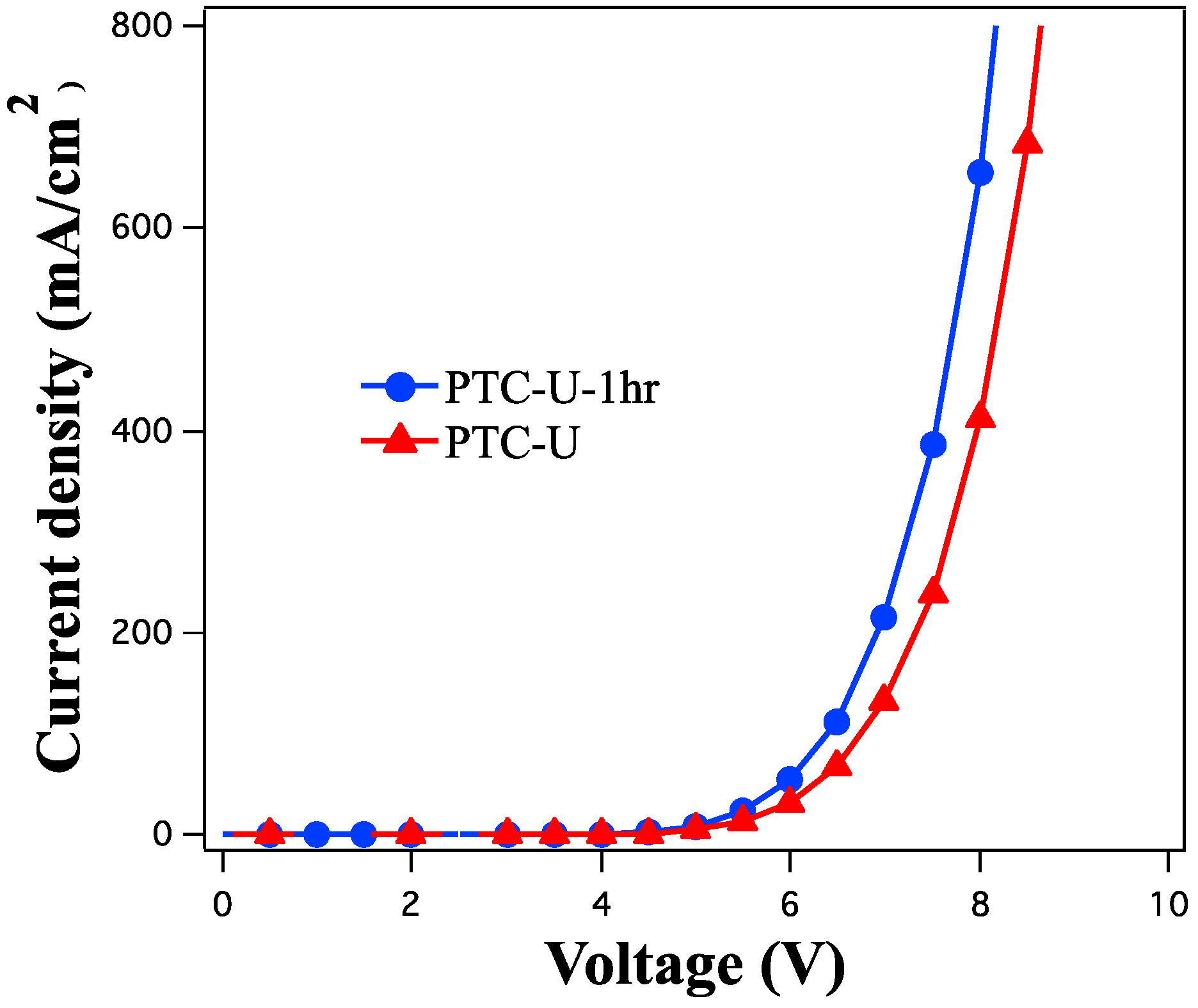
3.1. Physical and Electrical Properties

Scheme 1 displays our synthesis of PTC-U [27] and the structure of the product from photo-crosslinking of PTC-U through 2π + 2π photo-dimerization under UV light at 254 nm. When we subjected PTC-U to UV radiation, its pendent U bases underwent 2π + 2π photo-dimerization to form cyclobutane rings. This photo-crosslinking method would presumably improve the solvent resistance and thermal stability of PTC-U during the solution processing of multilayer OLEDs/PLEDs. Figure S3 presents UV-Vis spectra of the exposed PTC-U film. Upon exposure to UV light at 254 nm, the intensity of the absorption peak at 346 nm decreased gradually and the intensity of the absorption peak at 425 nm increased gradually, consistent with the occurrence of 2π + 2π photodimerization [30,31,32,33] and, therefore, an increase in the photo-crosslinking density of the pendent U units. High solvent resistant is a prerequisite for the fabrication of multilayer OLEDs/PLEDs through solution processing. We investigated the solvent resistance of our PTC-U film (before and after photo-crosslinking) by monitoring its UV-Vis spectra with chlorobenzene (a good solvent typically used for solution processing). Figure 1a–e presents the UV-Vis spectra recorded before and after rinsing of PTC-U and the photo-crosslinked products PTC-U-1hr, PTC-U-2hr, and PTC-U-4hr, respectively; Figure 1f displays a plot of the solvent resistance after the various UV irradiation times. After photo-crosslinking, all of the PTC-U films exhibited improved solvent resistance toward chlorobenzene.
We investigated the electrochemical characteristics of PTC-U-1hr thin film through CV (Figure 2), using tetrabutylammonium hexafluorophosphate (TBAPF6) as the supporting electrolyte and ferrocene as the internal standard, to assess the degree of charge injection of the polymer. The energy level of the highest occupied molecular orbital (HOMO) of PTC-U-1hr was approximately −5.15 eV (HOMO = −(Eox,onset + 4.8 eV), while the energy level of its lowest unoccupied molecular orbital (LUMO) was −2.12 eV. The electrochemical characteristics of PTC-U-1hr were the same as those of PTC-U, suggesting that PTC-U-1hr would also possess good electron-blocking properties and an appropriate energy level for use as an HITM in OLED device.
Scheme 1. Synthesis of compound PTC-U (3) and the structure of the photo-crosslinked polymer.
Polymers 07 00804 g007
Figure 1. (ae) UV-Vis spectra of PTC-U after exposure to UV irradiation for (a) 0 h; (b) 1 h; (c) 2 h; (d) 3 h; and (e) 4 h, both before and after rinsing with chlorobenzene (f) Solvent resistance (as measured by the ratio of absorption intensities before and after rinsing) plotted with respect to the UV irradiation time.
Polymers 07 00804 g001
Figure 2. Electrochemical characteristic of PTC-U-1hr.
Polymers 07 00804 g002
Furthermore, we also investigated the surface morphology of PTC-U, PTC-U-1hr, PTC-U-2hr, and PTC-U-4hr by AFM (Figure 3). The RMS roughness of PTC-U and PTC-U-1hr are almost the same (1.47 and 1.52 nm, respectively), and the RMS roughness of PTC-U-2hr and PTC-U-4hr are slightly increased after photo-crosslinking process (1.77 and 1.81 nm, respectively). However, compared to the AFM images and the RMS roughness of PTC-U, PTC-U-1hr, PTC-U-2hr, and PTC-U-4hr, we believe there is near-zero shrinkage in the course of photo-crosslinking.
Figure 3. AFM images of (a) PTC-U; (b) PTC-U-1hr; (c) PTC-U-2hr and (d) PTC-U-4hr coated on ITO glass. The average RMS roughness of each samples are PTC-U = 1.47 nm, PTC-U-1hr = 1.52 nm, PTC-U-2hr = 1.77 nm, PTC-U-4hr = 1.81 nm.
Polymers 07 00804 g003

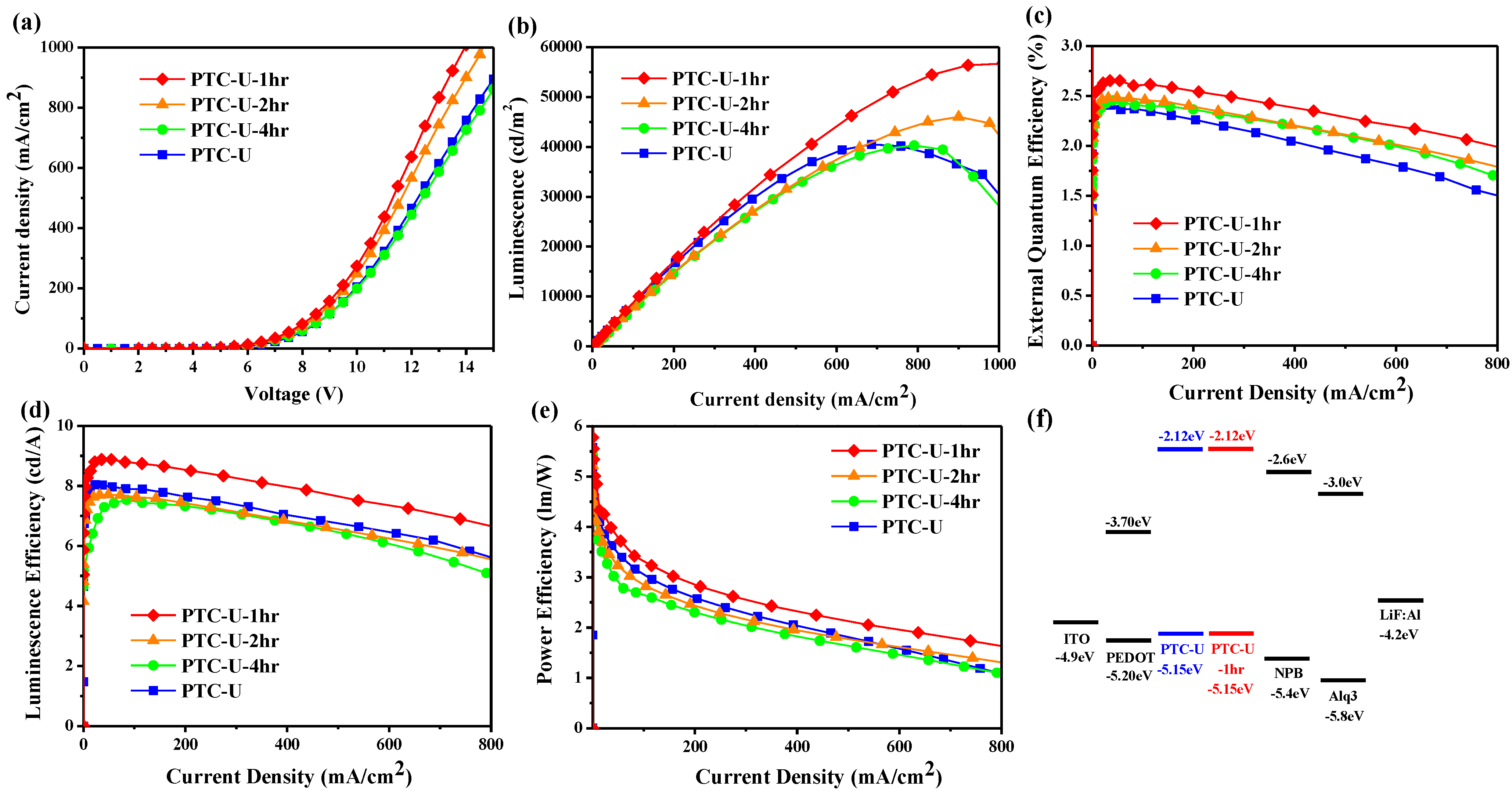
3.2. Florescence OLED Device

We tested the hole injection/transport ability of the crosslinked polymer through assembly of OLED devices through sequential coating of layers of PTC-U, PTC-U-1hr, PTC-U-2hr, or PTC-U-4hr (HITL), NPB (HTL), Alq3 (as the EML as well as the ETL (electron injection layer), LiF (as the EIL), and Al (electrode) onto ITO (transparent anode) (i.e., ITO/HITL (15 nm)/NPB (15 nm)/Alq3 (60 nm)/LiF (1 nm)/Al (100 nm) as shown in Scheme 2). When we used PTC-U or PTC-U-1hr as the HITL, the electroluminescence (EL) spectrum of the Alq3 dual-layer device peaked at 513 nm (Figure S4), indicating that PTC-U-1hr continued to serve only as a hole-transporting material, without causing exciplex formation. Figure 4 displays the current density–voltage–luminance (IVL) characteristics of these green light-emitting fluorescence devices. The operating voltage of the device based on PTC-U-1hr was almost the same as the control device incorporating the PTC-U at the same current density (Figure 4a); the turn-on voltage of the former (3.6 V, corresponding to the luminescence at 1 cd/m2) was almost the same as the latter (3.5 V). The major effect to determine turn-on voltage is the energy level OLED device structure, especially stepwise energy ladder HOMO level. Low tune-on voltage is the represent great hole injection ability. Low tune-on voltage represents the greater hole injection ability.
Scheme 2. Florescence OLED device structure: ITO/HITL/NPB/Alq3/LiF/Al.
Polymers 07 00804 g008
Figure 4. (a) IV; (b) LI; (c) EQE–I; (d) LE–I; (e) Power efficiency (PE)–I; and (f) energy gap characteristics of devices having the structure: ITO/HITL/NPB/Alq3/LiF/Al.
Polymers 07 00804 g004
However, the EQEs, LE, and PE represent the summation of hole injection ability and hole transporting ability of the OLED device. Figure 4b displays the luminescence plotted against the current density. The maximum luminescence of the device incorporating PTC-U-1hr (56,704 cd/m2) was 1.4 times that of the control device based on PTC-U (40,490 cd/m2). Figure 4c–e (Figure S5) display plots of the EQE, LE, and power efficiency (PE), respectively, against the current density. The EQEs of the devices incorporating PTC-U-1hr (2.65%), PTC-U-2hr (2.48%), and PTC-U-4hr (2.45%) were all higher than those of the control device based on PTC-U (2.4%), with that of the device incorporating PTC-U-1hr even being 1.8 times that of the corresponding device based on commercial PEDOT:PSS (1.46%) [27]. The LE and PE of the device incorporating PTC-U-1hr (8.9 cd/A and 5.5 lm/W, respectively) were 1.9 and 1.55 times higher, respectively, than those of the corresponding device based on commercial PEDOT:PSS (4.7 cd/A and 3.57 lm/W, respectively) [27].
The improvements in performance of the devices incorporating the photo-crosslinked PTC-U polymers, relative to the performance of the device based on non-crosslinked PTC-U, were due to their different HITLs, because the anode, cathode, ETL, EML, and EIL, and the thickness of each device, were identical. Because the HOMO energy levels of the photo-crosslinked PTC-U polymers (5.15 eV) were exactly the same as that of non-crosslinked PTC-U (5.15 eV), the energy barriers for hole injection and the electron blocking abilities would have been exactly the same for their different devices. The solvent resistance of the devices incorporating the irradiated PTC-U polymers improved as a result of photo-crosslinking. We attribute the enhanced brightness and efficiency of the device incorporating PTC-U-1hr, relative to those of the device based on PTC-U, to the balanced charge fluxes within the EML (the result of improved hole injection, hole transport, and solvent resistance). PTC-U and PTC-U-1hr were investigated by fabricating hole-only devices with structures of ITO/HITL (30 nm)/Al to further compare with the hole-transporting properties. The HITLs were coated on an ITO substrate using tetrachloroethane as solvent. The results are shown in Figure 5, where the current density (hole injecting/transporting ability) of the hole-only devices from the PTC-U-1hr increases as compared to PTC-U. The hole-transporting property improved form PTC-U to PTC-U-1hr due to the photo-crosslinking process. The photo-crosslinking improving the hole injecting and transporting ability of the devices incorporating the irradiated PTC-U polymers; accordingly, more holes moved to the emitting layer to balance the charge recombination at the emitting interface. Notably, the performance of the device having the structure ITO/PTC-U-1hr/NPB/Alq3/LiF/Al, in terms of its maximum brightness (56,704 cd/m2) and LE (8.9 cd/A), was higher than that of the previously reported multilayer device having the structure ITO/PEDOT:PSS/NPB/Alq3/LiF/Al [26,33], confirming the improvements in the hole injection, hole transport, and solvent resistance properties after the photo-crosslinking of PTC-U-1hr. Table 1 lists the characteristics of the EL obtained when using PTC-U, PTC-U-1hr, PTC-U-2hr, and PTC-U-4hr as HITMs. The maximum brightness and LE of PTC-U-2hr and PTC-U-4hr were disappointing, presumably because the UV radiation destroyed some of the covalent bonds (e.g., C–C, C–H, and C=C bonds) of the polymers [34,35,36,37].
Figure 5. IV characteristics of hole-only devices.
Polymers 07 00804 g005
Table 1. EL Data for Devices Having the Structure ITO/HITL/NPB/Alq3/LiF/Al.
HITLVon (V)Qmax (%)LEmax (cd/A)ηEmax (lm/W)Bmax (cd/m2)
PTC-U3.52.408.04.9840,490
PTC-U-1hr3.62.658.95.5556,704
PTC-U-2hr3.72.487.74.6546,027
PTC-U-4hr3.72.457.54.6540,288
PEDOT a2.41.464.73.5741,948
Note: a reference [27].

3.3. Phosphorescence OLED Device
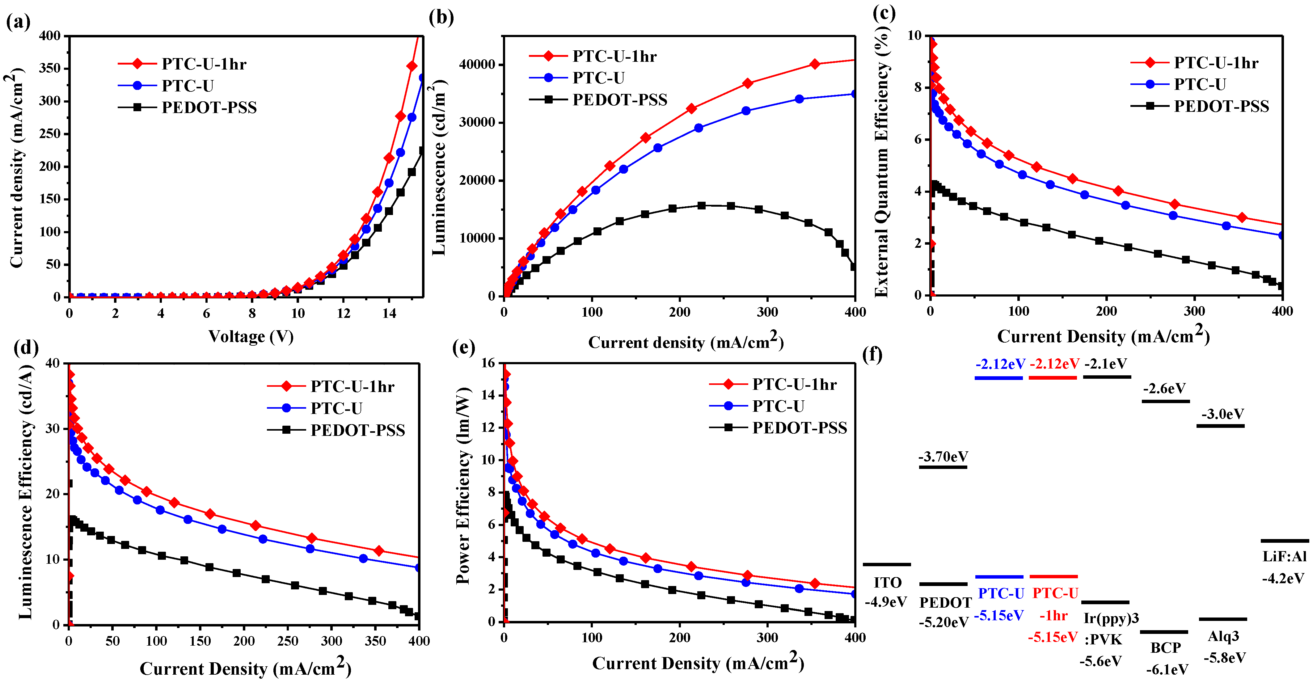
To further determine the suitability of using PTC-U-1hr for solution processing, we processed PTC-U-1hr, PTC-U, and PEDOT:PSS as the HITLs for Ir(ppy)3 (normal green light-emitting) phosphorescent OLEDs [38,39,40,41]. We formed the emissive layer (40 nm) through spin-coating of a blended solution of PVK and fac-tris(2-phenylpyridine)iridium(III) (Ir(ppy)3) in chlorobenzene (total 1.5 wt% in chlorobenzene, and 6 wt% for Ir(ppy)3:PVK). We then deposited BCP (10 nm), Alq3 (40 nm), LiF (1 nm), and Al (100 nm) as the hole blocking layer, electron transporting layer, and cathode, respectively, through thermal evaporation at a base pressure of less than 5 × 10⁻⁶ torr. We also fabricated a control device based on PEDOT:PSS (thickness When we used PTC-U or PTC-U-1hr as the HITL, the electroluminescence (EL) spectrum of the Ir(ppy)3:PVK device peaked at 512 nm (Figure S6), indicating that PTC-U-1hr continued to serve only as a hole-transporting material, without causing exciplex formation as the HITL layer (i.e., ITO/HITL (15 nm)/Ir(ppy)3:PVK (40 nm)/BCP (10nm)/Alq3 (40 nm)/LiF (1 nm)/Al (100 nm) as shown in Scheme 3). Figure 6a displays the IVL characteristics of these green light-emitting phosphorescent devices. The operating voltage of the device incorporating PTC-U-1hr was lower than that of the control device based on PEDOT:PSS at the same current density; the former also exhibited a lower turn-on voltage (7.13 V, corresponding to Figure 6a at 1 cd/m2; the same as that of the control device based on PTC-U). As mentioned above, the major effect to determine turn-on voltage is the energy level OLED device structure, especially stepwise energy ladder HOMO level. For our phosphorescent OLED device structure, PTC-U and PTC-U-1hr are having proper HOMO level to forming a stepwise energy ladder than PEDOT:PSS.
Scheme 3. Phosphorescence OLED device structure: ITO/HITL/Ir(ppy)3:PVK/BCP/Alq3/LiF/Al.
Polymers 07 00804 g009
Figure 6. (a) IV; (b) LI; (c) EQE–I; (d) LE–I; (e) PE–I; and (f) energy gap characteristics of devices having the structure: ITO/HITL/Ir(ppy)3:PVK/BCP/Alq3/LiF/Al.
Polymers 07 00804 g006
Figure 6b presents the luminescence plotted against the current density. The maximum luminescence of the device incorporating PTC-U-1hr (41,466 cd/m2) was 2.6 times that of the control device based on PEDOT:PSS (15,678 cd/m2). Figure 6c–e (Figure S7) displays plots of the EQE, LE, and PE, respectively, with respect to the current density. The EQE of the device incorporating PTC-U-1hr was 9.68%, nearly 2.3 times that of the control device based on PEDOT:PSS (4.29%). The LE and PE of the device incorporating PTC-U-1hr (36.6 cd/A and 15.32 lm/W, respectively) were 2.3 and 2.0 times, respectively, those of the control device based on PEDOT:PSS (16.2 cd/A and 7.85 lm/W, respectively). In addition, the EQE of the device incorporating PTC-U-1hr also improved, by 1.16 times, relative that of the control device based on PTC-U (8.35%). The LE and PE of the device incorporating PTC-U-1hr were 1.19 and 1.32 times, respectively, those of the control device based on PTC-U (30.8 cd/A and 11.65 lm/W, respectively).
The improvement in performance of the device incorporating PTC-U-1hr, relative to the device based on PTC-U, was due to the difference in solvent-resistance and hole-transporting properties after photo-crosslinking, because the anode, cathode, ETL, EML, EIL, and thickness of both devices were identical. The excellent solvent-resistance of PTC-U-1hr made it resistant to degradation during subsequent solution processing of the emitting layer (Ir(ppy)3:PVK in chlorobenzene). As mentioned above, the photo-crosslinking improving the hole injecting and transporting ability of the devices incorporating the irradiated PTC-U polymers, in Figure 5. Notably, the performance of the ITO/PTC-U-1hr/Ir(ppy)3:PVK/BCP/Alq3/LiF/Al device, in terms of maximum brightness (41,466 cd/m2) and LE (36.6 cd/A), was superior to that of the previously reported multilayer device having the structure ITO/PEDOT:PSS/Ir(ppy)3:PVK/BCP/Alq3/LiF/Al [42,43,44]. Table 2 lists the EL characteristics of the devices incorporating PTC-U-1hr and PTC-U as HITMs.
Table 2. EL Data for Devices Having the Structure ITO/HITL/Ir(ppy)3:PVK/BCP/Alq3/LiF/Al.
HITLVon (V)Qmax (%)LEmax (cd/A)ηEmax (lm/W)Bmax (cd/m2)
PTC-U-1hr7.139.6836.615.3241,466
PTC-U7.138.3530.811.6534,978
PEDOT7.334.2916.27.8515,678

4. Conclusions

We have developed a new process—through photo-crosslinking of PTC-U for 1hr—for preparing an HITL material displaying excellent solvent-resistance and hole injection and hole transport ability. The efficiency of PTC-U-1hr when used as an HITL led to excellent improvements in the performance of both fluorescent and phosphorescent OLED devices. More importantly, the performance of the solution-processed device incorporating PTC-U-1hr was excellent when compared with those of corresponding the control device based on PTC-U and commercial PEDOT: PSS. Accordingly, PTC-U-1hr appears to be a promising HITM for use in highly efficient solution-processed phosphorescent OLEDs. PTC-U-1hr allowed us to construct a fluorescent device (an electroluminescent device having the structure ITO/HITL/1,4-bis[(1-naphthyl)phenylamino] diamine (NPB)/tris(8-hydroxyquinolinato) aluminum (Alq3)/LiF/Al) exhibiting a maximum brightness as high as 56,704 cd/m2 and an EQE and LE of 2.65% and 8.9 cd/A, respectively. Furthermore, we also fabricated a phosphorescent device (an electroluminescent device having the structure ITO/HITL/Ir(ppy)3:polyvinylcarbazole (PVK)/2,9-dimethyl-4,7-diphenyl-1,10-phenanthroline (BCP)/Alq3/LiF/Al) that achieved a maximum brightness as high as 41,466 cd/m2 and an EQE and LE of 9.68% and 48 cd/A, respectively. The presence of PTC-U-1hr in a phosphorescent OLED prepared through solution processing resulted in EQEs and LEs that were 2.2 times higher than thos Accordingly, PTC-U-1hr appears to be a promising HITM for use in highly efficient solution-processed phosphorescent OLEDs.e of the corresponding device based on commercial PEDOT:PSS.

Acknowledgments

This study was supported financially by the Ministry of Science and Technology, Taiwan, under contracts MOST103-2221-E-110-079-MY3 and MOST102-2221-E-110-008-MY3. We thank Chien-Hong Cheng (National Tsing Hua University) for his support and assistance during the preparation and characterization of the OLED devices.

Author Contributions

Hsi-Kang Shih, Yi-Han Chen, and Yu-Lin Chu contributed to the fabrication of OLED device and instrumental analysis of the data; Yu-Lin Chu synthesised the materials; Yu-Lin Chu and Chih-Chia Cheng designed the experiment; Feng-Chih Chang, Chao-Yuan Zhu, and Shiao-Wei Kuo coordinated the study, interpreted the results and discussion and contributed to the writing of the paper; Feng-Chih Chang contributed to the writing of the paper; Hsi-Kang Shih wrote the paper.

Supplementary Information

The TGA, DSC, UV and device fabrication information can be accessed at https://www.mdpi.com/2073-4360/7/5/0804/s1.

References

  1. Forrest, S.R. The path to ubiquitous and low-cost organic electronic appliances on plastic. Nature 2004, 428, 911–918. [Google Scholar] [CrossRef] [PubMed]
  2. McCarthy, M.A.; Liu, B.; Donoghue, E.P.; Kravchenko, I.; Kim, D.Y.; So, F.; Rinzler, A.G. Low-voltage, low-power, organic light-emitting transistors for active matrix displays. Science 2011, 332, 570–573. [Google Scholar] [CrossRef] [PubMed]
  3. Park, J.W.; Shin, D.C.; Park, S.H. Large-area OLED lightings and their applications. Semicond. Sci. Technol. 2011, 26. [Google Scholar] [CrossRef]
  4. Kim, J.Y.; Joo, C.W.; Lee, J.; Woo, J.-C.; Oh, J.-Y.; Baek, N.S.; Chu, H.Y.; Lee, J.-I. Save energy on OLED lighting by a simple yet powerful technique. RSC Adv. 2015, 5, 8415–8421. [Google Scholar] [CrossRef]
  5. Strukelj, M.; Papadimitrakopoulos, F.; Miller, T.M.; Rothberg, L.J. Design and application of electron-transporting organic materials. Science 1995, 267, 1969–1972. [Google Scholar] [CrossRef] [PubMed]
  6. Burroughes, J.H.; Bradley, D.D.C.; Brown, A.R.; Marks, R.N.; Mackay, K.; Friend, R.H.; Burns, P.L.; Holmes, A.B. Light-emitting diodes based on conjugated polymers. Nature 1990, 347, 539–541. [Google Scholar] [CrossRef]
  7. Ji, W.; Wang, J.; Zeng, Q.; Su, Z.; Sun, Z. Highly efficient organic light-emitting devices by introducing traps in the hole-injection layer. RSC Adv. 2013, 3, 14616–14621. [Google Scholar] [CrossRef]
  8. Granström, M.; Berggren, M.; Inganäs, O. Micrometer- and nanometer-sized polymeric light-emitting diodes. Science 1995, 267, 1479–1481. [Google Scholar] [CrossRef] [PubMed]
  9. Ho, P.K.H.; Kim, J.S.; Burroughes, J.H.; Becker, H.; Li, S.F.Y.; Brown, T.M.; Cacialli, F.; Friend, R.H. Molecular-scale interface engineering for polymer light-emitting diodes. Nature 2000, 404, 481–484. [Google Scholar] [CrossRef] [PubMed]
  10. Carter, S.A.; Angelopoulos, M.; Karg, S.; Brock, P.J.; Scott, J.C. Polymeric anodes for improved polymer light-emitting diode performance. Appl. Phys. Lett. 1997, 70, 2067–2069. [Google Scholar] [CrossRef]
  11. De Jong, M.P.; van Ijzendoorn, L.J.; de Voigt, M.J.A. Stability of the interface between indium-tin-oxide and poly(3,4-ethylenedioxythiophene)/poly(styrenesulfonate) in polymer light-emitting diodes. Appl. Phys. Lett. 2000, 77, 2255–2257. [Google Scholar] [CrossRef]
  12. Baranoff, E.; Curchod, B.F.E.; Frey, J.; Scopelliti, R.; Kessler, F.; Tavernelli, I.; Rothlisberger, U.; Graẗzel, M.; Nazeeruddin, Md.K. Acid-induced degradation of phosphorescent dopants for OLEDs and its application to the synthesis of tris-heteroleptic iridium(III) bis-cyclometalated complexes. Inorg. Chem. 2012, 51, 215–224. [Google Scholar] [CrossRef] [PubMed]
  13. Schaer, M.; Nüesch, F.; Berner, D.; Leo, W.; Zuppiroli, L. Water vapor and oxygen degradation mechanisms in organic light emitting diodes. Adv. Funct. Mater. 2001, 11, 116–121. [Google Scholar] [CrossRef]
  14. Hittinger, E.; Kokil, A.; Weder, C. Synthesis and characterization of cross-linked conjugated polymer milli-, micro-, and nanoparticles. Angew. Chem. Int. Ed. 2004, 43, 1808–1811. [Google Scholar] [CrossRef]
  15. Weder, C. Synthesis, processing and properties of conjugated polymer networks. Chem. Commun. 2005, 43, 5378–5389. [Google Scholar] [CrossRef]
  16. Niu, Y.H.; Liu, M.S.; Ka, J.W.; Bardker, J.; Zin, M.T.; Schofield, R.; Chi, Y.; Jen, A.K.Y. Crosslinkable hole-transport layer on conducting polymer for high-efficiency white polymer light-emitting diodes. Adv. Mater. 2007, 19, 300–304. [Google Scholar] [CrossRef]
  17. Cheng, Y.J.; Liu, M.S.; Zhang, Y.; Niu, Y.; Huang, F.; Ka, J.W.; Yip, H.L.; Tian, Y.; Jen, A.K.Y. Thermally cross-linkable hole-transporting materials on conducting polymer: Synthesis, characterization, and applications for polymer light-emitting devices. Chem. Mater. 2008, 20, 413–422. [Google Scholar] [CrossRef]
  18. Su, W.F.; Chen, Y. Synthesis and optoelectronic properties of a luminescent fluorene derivative containing hole-transporting triphenylamine terminals. Polymer 2011, 52, 3311–3317. [Google Scholar] [CrossRef]
  19. Cha, S.J.; Cho, S.N.; Lee, W.H.; Chung, H.S.; Kang, I.N.; Suh, M.C. Thermally cross-linkable hole transport polymers for solution-based organic light-emitting diodes. Macromol. Rapid Commun. 2014, 35, 807–812. [Google Scholar] [CrossRef] [PubMed]
  20. Karthik, D.; Thomas, K.R.J.; Jou, J.-H.; Kumar, S.; Chen, Y.-L.; Jou, Y.-C. Deep-blue emitting pyrene-benzimidazole conjugates for solution processed organic light-emitting diodes. RSC Adv. 2015, 5, 8727–8738. [Google Scholar] [CrossRef]
  21. Bacher, E.; Bayerl, M.; Rudati, P.; Reckefuss, N.; Müller, C.D.; Meerholz, K.; Nuyken, O. Synthesis and characterization of photo-cross-linkable hole-conducting polymers. Macromolecules 2005, 38, 1640–1647. [Google Scholar] [CrossRef]
  22. Jungermann, S.; Riegel, N.; Müller, C.D.; Meerholz, K.; Nuyken, O. Novel photo-cross-linkable hole-transporting polymers: Synthesis, characterization, and application in organic light emitting diodes. Macromolecules 2006, 39, 8911–8919. [Google Scholar] [CrossRef]
  23. Solomeshch, O.; Yu, Y.-J.; Medvedev, V.; Razin, A.; Blumer-Ganon, B.; Eichen, Y.; Jin, J.-I.; Tessler, N. Wide band gap cross-linkable semiconducting polymer LED. Synth. Met. 2007, 157, 841–845. [Google Scholar] [CrossRef]
  24. Solomeshch, O.; Medvedev, V.; Mackie, P.R.; Cupertino, D.; Razin, A.; Tessler, N. Electronic formulations—Photopatterning of luminescent conjugated polymers. Adv. Funct. Mater. 2006, 16, 2095–2102. [Google Scholar] [CrossRef]
  25. Kohnen, A.; Riegel, N.; Kremer, J.H.-W.M.; Lademann, H.; Müller, D.C.; Meerholz, K. The simple way to solution-processed multilayer OLEDs—Layered block-copolymer networks by living cationic polymerization. Adv. Mater. 2009, 21, 879–884. [Google Scholar] [CrossRef]
  26. Cheng, C.C.; Yen, Y.C.; Ye, Y.S.; Chang, F.C. Biocomplementary interaction behavior in DNA-like and RNA-like polymers. J. Polym. Sci. Polym. Chem. 2009, 47, 6388–6395. [Google Scholar] [CrossRef]
  27. Chu, Y.L.; Cheng, C.C.; Yen, Y.C.; Chang, F.C. A new supramolecular hole injection/transport material on conducting polymer for application in light-emitting diodes. Adv. Mater. 2012, 24, 1894–1898. [Google Scholar] [CrossRef] [PubMed]
  28. Lee, T.W.; Kwon, Y.; Park, J.J.; Pu, L.; Hayakawa, T.; Kakimoto, M.-A. Novel hyperbranched phthalocyanine as a hole injection nanolayer in organic light-emitting diodes. Macromol. Rapid Commun. 2007, 28, 1657–1662. [Google Scholar] [CrossRef]
  29. Lee, T.W.; Park, J.J.; Kwon, Y.; Hayakawa, T.; Choi, T.L.; Park, J.H.; Das, R.R.; Kakimoto, M.-A. Spin-assembled nanolayer of a hyperbranched polymer on the anode in organic light-emitting diodes: The mechanism of hole injection and electron blocking. Langmuir 2008, 24, 12704–12709. [Google Scholar] [CrossRef] [PubMed]
  30. Setlow, R.B. Cyclobutane-type pyrimidine dimers in polynucleotides. Science 1966, 153, 379–386. [Google Scholar] [CrossRef] [PubMed]
  31. Blackburn, G.M.; Davies, R.J.H. The structure of thymine photo-dimer. J. Chem. Soc. C 1966, 23, 2239–2244. [Google Scholar] [CrossRef]
  32. Wang, Y.S.; Cheng, C.C.; Ye, Y.S.; Yen, Y.C.; Chang, F.C. Bioinspired photo-cross-linked nanofibers from uracil-functionalized polymers. ACS Macro Lett. 2012, 1, 159–162. [Google Scholar] [CrossRef]
  33. Tominaga, M.; Konishi, K.; Aida, T. A Photocrosslinkable dendrimer consisting of a nucleobase. Chem. Lett. 2000, 29, 374–375. [Google Scholar] [CrossRef]
  34. Thangthong, A.-M.; Prachumrak, N.; Tarsang, R.; Keawin, T.; Jungsuttiwong, S.; Sudyoadsuk, T.; Promarak, V. Blue light-emitting and hole-transporting materials based on 9,9-bis(4-diphenylaminophenyl)fluorenes for efficient electroluminescent devices. J. Mater. Chem. 2012, 22, 6869–6877. [Google Scholar] [CrossRef]
  35. Zhang, Y.D.; Hreha, R.D.; Jabbour, G.E.; Kippelen, B.; Peyghambarian, N.; Marder, S.R. Photo-crosslinkable polymers as hole-transport materials for organic light-emitting diodes. J. Mater. Chem. 2002, 12, 1703–1708. [Google Scholar] [CrossRef]
  36. Huang, F.; Cheng, Y.J.; Zhang, Y.; Liu, M.S.; Jen, A.K.Y. Crosslinkable hole-transporting materials for solution processed polymer light-emitting diodes. J. Mater. Chem. 2008, 18, 4495–4509. [Google Scholar] [CrossRef]
  37. Lee, J.; Han, H.; Lee, J.; Yoon, S.H.; Lee, C. Utilization of “thiol-ene” photo cross-linkable hole-transporting polymers for solution-processed multilayer organic light-emitting diode. J. Mater. Chem. C 2014, 2, 1474–1481. [Google Scholar] [CrossRef]
  38. Baldo, M.A.; Lamansky, S.; Burrows, P.E.; Thompson, M.E.; Forrest, S.R. Very high-efficiency green organic light-emitting devices based on electrophosphorescence. Appl. Phys. Lett. 1999, 75, 4–6. [Google Scholar] [CrossRef]
  39. Lee, C.L.; Lee, K.B.; Kim, J.J. Polymer phosphorescent light-emitting devices doped with tris(2-phenylpyridine) iridium as a triplet emitter. Appl. Phys. Lett. 2000, 77, 2280–2282. [Google Scholar] [CrossRef]
  40. Kawamura, Y.; Yanagida, S.; Forrest, S.R. Energy transfer in polymer electrophosphorescent light emitting devices with single and multiple doped luminescent layers. J. Appl. Phys. 2002, 92, 87–93. [Google Scholar] [CrossRef]
  41. Gong, X.; Robinson, M.R.; Ostrowski, J.C.; Moses, D.; Bazan, G.C.; Heeger, A.J. High-efficiency polymer-based electrophosphorescent devices. Adv. Mater. 2002, 14, 581–585. [Google Scholar] [CrossRef]
  42. Lee, C.C.; Yeh, K.M.; Chen, Y. New host homopolymers containing pendant triphenylamine derivatives: Synthesis, optical, electrochemical properties and its blend with Ir(ppy)3 for green phosphorescent organic light-emitting devices. J. Polym. Sci. Polym. Chem. 2008, 46, 7960–7971. [Google Scholar] [CrossRef]
  43. Yeh, K.M.; Lee, C.C.; Chen, Y. Vinyl polymer containing 1,4-distyrylbenzene chromophores: synthesis, optical, electrochemical properties and its blend with PVK and Ir(ppy)3. Synth. Met. 2008, 158, 411–416. [Google Scholar] [CrossRef]
  44. Yang, M.J.; Tsutsui, T. Use of poly(9-vinylcarbazole) as host material for iridium complexes in high-efficiency organic light-emitting devices. Jpn. J. Appl. Phys. 2000, 39, 828–829. [Google Scholar] [CrossRef]

