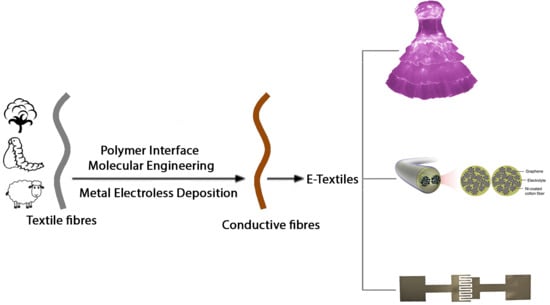
Polymer Interface Molecular Engineering for E-Textiles


School of Materials, University of Manchester, Oxford Road, Manchester M13 9PL, UK
*
Author to whom correspondence should be addressed.
Polymers 2018, 10(6), 573; https://doi.org/10.3390/polym10060573
Submission received: 30 April 2018
/
Revised: 18 May 2018
/
Accepted: 21 May 2018
/
Published: 23 May 2018
(This article belongs to the Special Issue Polymer Processing for Enhancing Textile Application)
Abstract
:Wearable electronics, regarded as the next generation of conventional textiles, have been an important concept in the study of e-textiles. Conductive fibres are the upstreaming of e-textiles and have witnessed the booming development in recent years. However, little work has focused on improving the wash ability and durability of conductive fibres. As a new approach to manufacturing conductive fibres, Polymer Interface Molecular Engineering (PIME) is starting to be employed recently, to build up an interfacial layer on polymeric fibre surfaces; this interfacial layer services as a platform to anchor catalysts for the following metal Electroless Deposition (ELD). The designed interfacial layer significantly increases adhesion between polymeric substrates and coating metal layers, to improve the durability of e-textiles. This review highlights recent research into different molecular and architectural design strategies, and its potential application for wearable electronics. Further challenges and opportunities in this field are also discussed critically.
1. Introduction
In recent years, researchers have shown an increased interest in wearable electronics, which have a wide range of applications, such as photodynamic therapy, flexible batteries, heating fabrics and wearable displays [1,2,3,4,5,6,7,8,9,10,11,12,13,14]. The fabrication of conductive components into flexible electronics is a key problem in achieving large scale production of smart textiles. There are a large number of published studies that report on conductors integrated with flexible substrates such as carbon materials, conducting polymers and metal [4,9,15]. Carbon black is an intrinsic black product which causes negative effects to the aesthetics of textiles. Graphene has no scaling up products and people are still seeking efficient technology in the exploitation of single layer graphene. Conductive polymers are very expensive and have relatively lower conductivity. Among these materials, metal is the most popular conductive material because it is cheap, highly conductive and widely compatible. For the intergradation of metal materials into flexible substrates and fibres, improving adhesion force is the key for the durability of e-textile and wearable electronics.
Several studies have attempted to coat metal nanoparticles onto soft substrates through techniques such as vapour phase deposition [16], chemical vapour deposition [17,18,19] and electro-deposition [20,21,22]. However, the fabrication via such methods does not have chemical bonds or any other tethering force between the metallic layer and the original substrates. The poor adhesion between the coating layer and the substrates limits the widespread application of wearable devices. Electroless deposition (ELD) is a low cost and simple method [23,24] for fabricating metal films (Cu, Ni, Ag, Au, etc.) on soft and stretchable substrates such as rubber, plastic, leaves and fabrics [9,25,26]. The polymer interface plays an important role during the whole ELD process because the surface modification significantly increases the adhesion between metal nanoparticles and flexible substrates [27]. The conventional process for Polymer Interface Molecular Engineering (PIME) catalytic ELD is illustrated in Figure 1. The first step is to modify raw substrates by grafting a polymer onto them; the second step involves the immobilisation of captured catalysts; the third step entails electroless deposition, whereby metal nanoparticles grow on the catalysed area [4,9].
2. Polymer Interface and Catalytic Moiety
Recent decades have witnessed the development of various techniques for grafting polymers onto flexible substrates, such as self-crosslinking copolymerisation, free radical polymerisation (FRP), and surface-initiated atom transfer radical polymerisation (SI ATRP) [28,29], as shown in Figure 2. Additionally, there have been several academic studies on ELD relating to radiation-induced [30], plasma-induced [31] and UV-triggered polymerisation [32]. SI ATRP is a popular approach as it produces a high-density polymer layer; however, it also has some disadvantages, such as low productivity and a nitrogen atmosphere. FRP is conducted in an air environment and the thickness of the polymer interfacial layer ranges from tens to hundreds of nanometres [9]. Nevertheless, FRP requires pre-treatment (vinyl-terminating silane modification) before the polymerisation of poly[2-(methacryloyloxy)-ethyl]-trimethylammonium chloride (PMETAC), and can only produce conductive cotton yarns/fabrics without the plasma treatment.
Polyphenols, such as dopamine and tannic acid, are at the cutting edge of the PIME catalytic ELD field. Dopamine is a type of biomaterial found in mussels and can, through self-polymerisation in an aqueous solution at pH 8.5, form an adhesive film on a wide range of inorganic and organic materials, including fabrics, polymers and ceramics. More importantly, the robust film can continuously conduct various secondary treatments, including ELD at room temperature, without any specific equipment [33]. Tannic acid (TA) is usually extracted from plants such as gallnuts. Due to the numerous phenol groups in its structure, TA has excellent metal ions-chelating ability and can bind other materials via hydrogen bonds [34].
Modern polymer matrices (cationic, anionic, nonionic and polyphenols) can be used in PIME catalytic ELD for flexible electronic industries. Poly[2-(meth acryloy loxy)-ethyl]trimethylammonium chloride (PMETAC) [35,36,37,38,39] and poly(acrylic acid) (PAA) [40,41,42] are the two most common polymer interfaces, as both have the technical feasibility to synthesise and select marked catalytic moieties. Polyphenols are state-of-the-art polymer interfaces and have unexceptional properties for coating metal nanoparticles onto flexible and/or stretchable substrates.
2.1. Cationic Polymer Interface and Catalytic Moiety
The cationic polymer interface is defined as a positively charged polyelectrolyte, which has a powerful affinity to the anionic catalytic moieties. PMETAC is a cationic polymer interface that is widely used to transfer ion species such as [PdCl4]2−. Liu et al. [43] reported that surface plasma treated poly(ethylene terephthalate) (PET) yarns/fabrics were immobilised with an ATRP initiator, and PMETAC was then employed to modify PET yarns/fabrics, after which catalytic moieties [PdCl4]2− were loaded onto the fibre surface with the help of grafted PMETAC. The quaternary ammonium groups of PMETAC have a particular ability to anchor [PdCl4]2− species, and catalytic areas were formed by ion exchange. The thin copper film was finally grown on the catalytic surface by immersing modified PET substrates into a copper ELD bath [43], as shown in Figure 3. The thickness of the copper film is determined by the amount of the catalyst, which depends on the concentration of [PdCl4]2− species in the aqueous solution. The copper/PET hierarchical structures of the polymer bridges present excellent selectivity because deposition only takes place in the zone covered by the catalyst.
2.2. Anionic Polymer Matrix and Catalytic Moiety
The anionic polymer matrix is defined as a negatively charged polyelectrolyte which can immobilise the cationic moieties in the aqueous solution. The two most common anionic polymer models are poly(acrylic acid) (PAA) [40,41,42] and poly(meth acryloyl ethyl phosphate) (PMEP). PAA brushes negatively charged at an appropriate pH can tightly bind metal cations, such as Ni2+, Cu2+ and [Pd(NH3)4]2+ [4]. According to Kobersterin et al. [42], after a PAA interface catalytic ELD had been introduced, a block copolymer polystyrene-b-poly(tertbutyl acrylate) (PS-b-PtBA) was applied. In the first step, the polystyrene blocks penetrated a polystyrene substrate and the PtBA blocks were exposed to ultraviolet (UV) radiation, after which a photoacid generator hydrolysed them to yield PAA blocks. In the next step, PAA brushes captured catalytic ions ([Pd(NH3)4]2+) and a thin nickel layer was coated onto [Pd(NH3)4]2+ areas in a nickel ELD bath, as illustrated in Figure 4. In principle, this approach can be applied to all kinds of substrates, provided the original substrate and the first polymer block are the same.
More recently, ligand-induced electroless plating (LIEP) was introduced for forming metal structures on polymer substrates [40,44,45]. To be precise, PAA was grown on polymer substrates via a GraftFast method, in which vinylic monomers were initiated by radical polymerisation in an aqueous solution (radicals were created by the reduction reaction of aryl- diazonium salts with iron powder) [46]. The PAA-modified substrate was immersed in a bath of alkaline solution containing Cu2+ ions and ammonia. Carboxylate groups of PAA then absorbed Cu2+ ions, and these absorbed ions were subsequently reduced by NaBH4. Finally, a thin copper film was fabricated on the polymer substrate, as shown in Figure 5. The LIEP system does not require an expensive palladium catalyst and can be used in many polymer substrates, such as polystyrene (PS), acrylonitrile-butadiene-styrene copolymer (ABS), polybutadiene (PB), poly(vinylidene fluoride) (PVDF), polyethylene terephthalate (PET) and polyacrylonitrile (PAN).
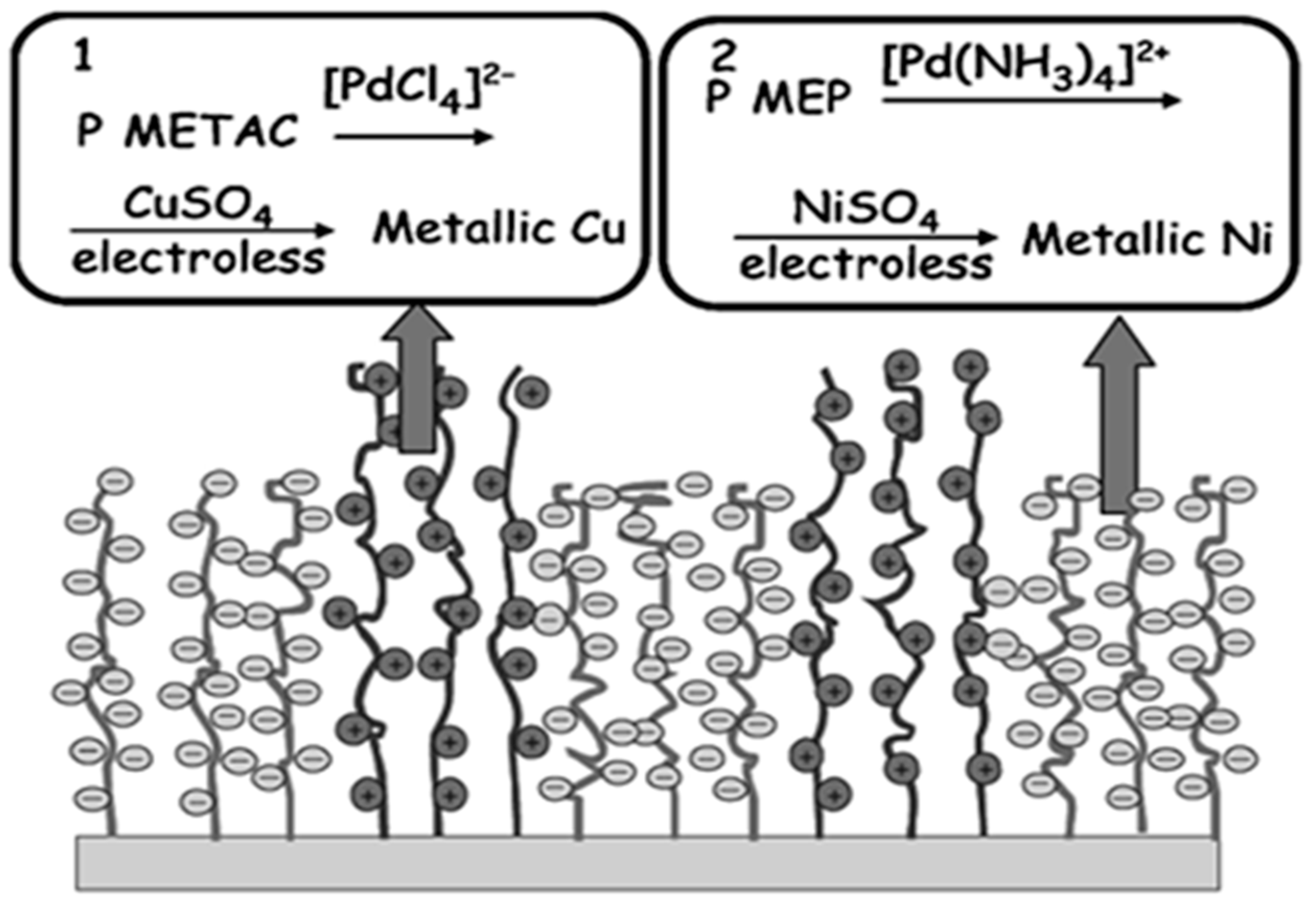
PMEP, reported by Zheng, is another approach of anionic polymer matrix for ELD; the two oppositely charged polymer brushes have a strong affinity to various metal ions for site-selective ELD [47]. PMETAC and PMEP were synthesised by micro-contact printing and surface-initiated atom transfer radical polymerisation, respectively. [PdCl4]2− species were captured via the quaternary ammonium groups of the PMETAC layer, which was positively charged, while [Pd(NH3)4]2+ ions were immobilised by the phosphate groups of PMEP chains, which were negatively charged. Two types of metal nanoparticles, Cu and Ni, were then deposited onto flexible substrates by immersing them into the ELD solution of copper and nickel, respectively, as shown in Figure 6. This method uses binary polymer brushes, acting as two seeding templates, to fabricate bimetallic layers on substrates.
2.3. Nonionic Polymer Interface and Catalytic Moiety
Nonionic polymers are another powerful polyelectrolyte with a strong affinity for related metal ionic catalysts of PIME catalytic ELD, including polyacrylonitrile (PAN), polyacrylamide (PAM), poly(vinyl pyrrolidone) (PVP), poly(2-vinyl pyridine) (P2VP) and poly(4-vinyl pyridine) (P4VP). There are two distinct properties of nonionic polymers: (1) In the presence of free nitrogen electron pairs, catalysts can be anchored onto the binding sites via ion exchange; (2) many polymers such as polyethylene (PE), polypropylene (PP), polyimide (PI), poly(tetrafluoroethylene) (PTFE), fluorinated polyimide (FPI) and poly-(tetrafluoroethylene-co-hexafluoropropylene) (FEP) can be used to modify substrates by various polymerisation techniques (radiation-, UV-, or plasma-induced polymerisation and SI ATRP). An advantage of this approach is that the polymerisation or copolymerisation of these nonionic polymers has the possibility of second processing, high productivity and large-scale production. More importantly, only simple devices are required to conduct the experiment.
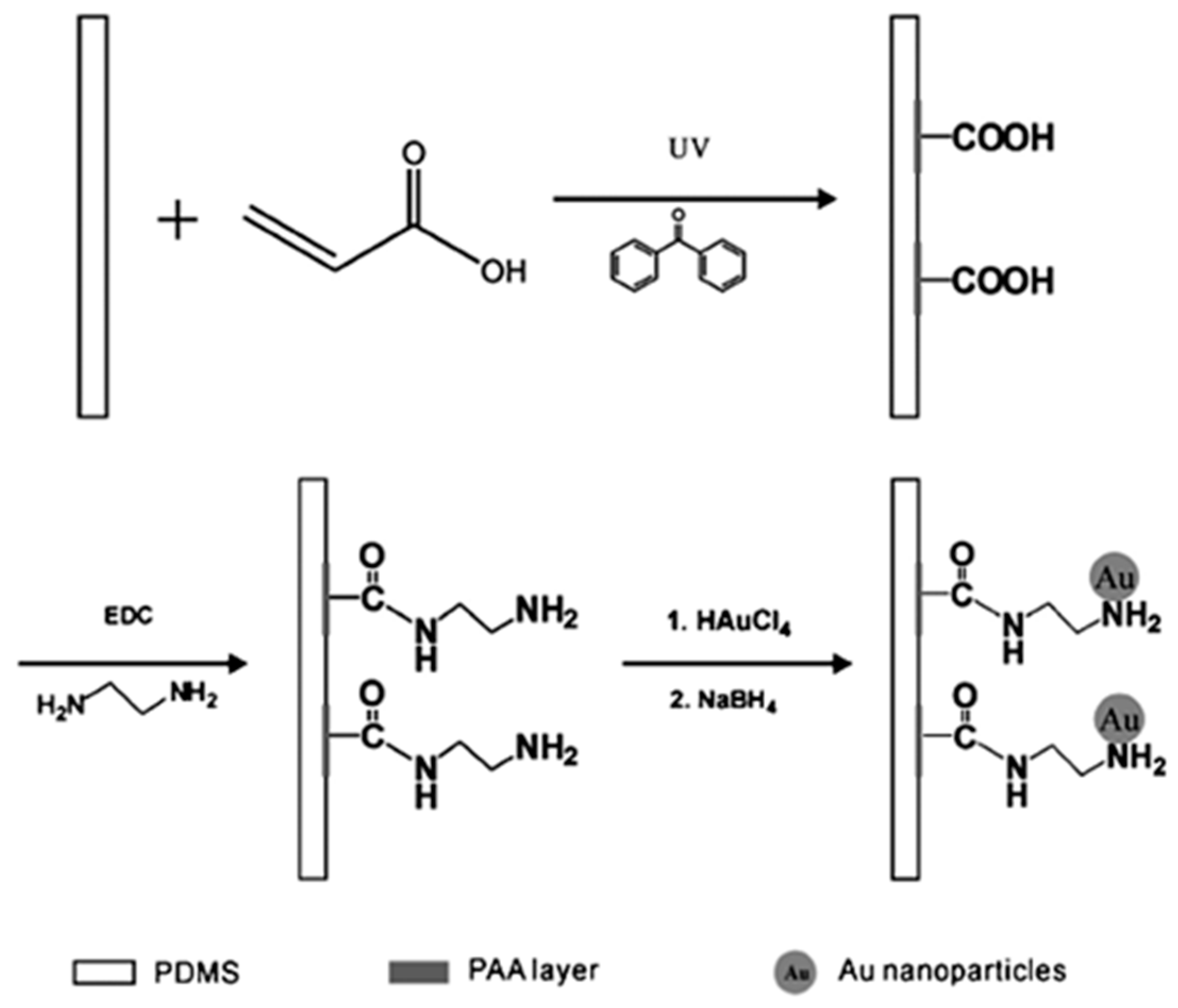
Kang et al. [48,49,50] mentioned that N-containing nonionic polymer brushes could be polymerised on flexible substrates through post-modification of surface-grafted polymeric polyelectrolytes. Moreover, Yu et al. [51] found a strong adhesion after testing the metal layers that were plated onto these post-modified surface-grafted polymer brushes. Chen et al. [52] fabricated post-modified PAA into amine-terminating layers, which were then used to synthesise a gold film by ELD, as illustrated in Figure 7. UV-induced polymerisation was applied on a poly(dimethylsiloxane) (PDMS) substrate to trigger the synthesis of the PAA layer; ethylenediamine then modified the patterned PAA interface, which had carboxylic acid groups, to create new polymers with amine-terminating groups. These polymers were finally used to immobilise the gold nanoparticles. The results showed that a superior adhesion between the gold thin film and the PDMS surface was produced.
2.4. Polyphenols Interface and Catalytic Moiety
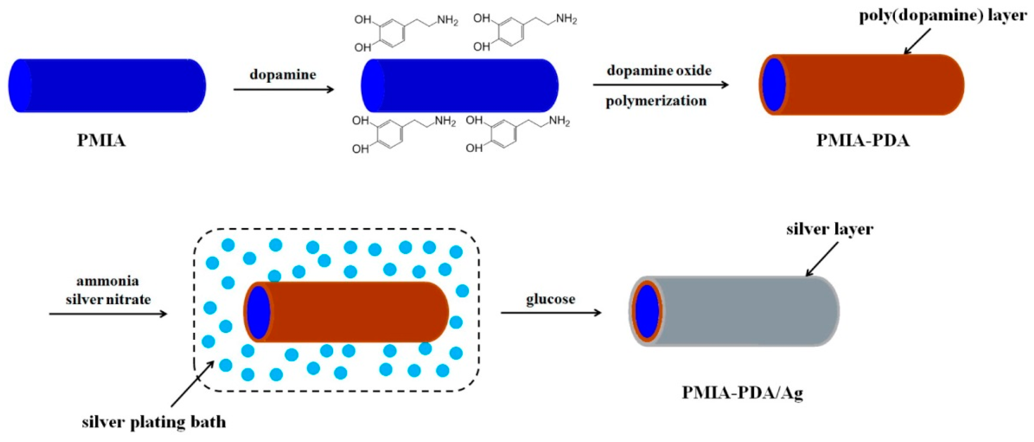
Polyphenols are a totally new polyelectrolyte, which have the strong ability to chelate related catalysts. The two most popular polyphenols applied in ELD are dopamine and tannic acid, whose unparalleled properties and attributes offer them a bright future in PIME catalytic ELD. Wang et al. [53] reported research of dopamine-assisted ELD, as shown in Figure 8. Polymetapheny-lene isophthamide (PMIA) fibres were coated with a layer of polydopamine (PDA) by immersing PMIA into an alkaline dopamine solution. This adhesive film then immobilised silver ions by chemical bonding. Glucose was subsequently added to the silver electroless plating bath to reduce silver ions into silver nanoparticles, and finally formed a silver layer on the PMIA surface. PDA-based PIME catalytic ELD is a simple, efficient and eco-friendly method.
Li et al. [34] presented research related to Tannic Acid (TA), as illustrated in Figure 9. According to their report, TA formed intermolecular hydrogen bonds with catkin fibres, which have hydroxyl groups that are advantageous for capturing TA-Fe coordination complexes on the catkin surface. Silver nanoparticles were then formed in situ on the fibre surface, acting as nucleation sites for later electroless silver coating. The TA polymer interface is firmly immobilised by chemical and/or physical reactions during the ELD process. More importantly, the polymer chains which have specific ligands can anchor the silver catalytic ions and yield robust adhesion. This technique has some advantages over PDA, although the PDA interface can form on many flexible solid substrates at room temperature without any pre-treatments, dopamine is expensive and the self-assembly of PDA is time consuming.
3. Substrates and Applications of ELD in Wearable Electronics
PIME catalytic ELD has been introduced as a highly productive method for fabricating metal conductors in flexible and stretched electronics [9]. Crucial components of this technique include not only the polymer interfaces and catalytic moieties, but also the different kinds of substrates used (metals, glass, rubbers, cotton and some biomimetic materials) [10], which have a significant impact on the properties of ELD electronics.
3.1. ELD on Plastic Substrates
PIME catalytic ELD is synthesised under simple conditions involving room temperature treatment and cheap equipment [23,24], which is ideal for plastic substrates. One report described how a thin copper electrode was formed through ELD, with the help of ligand-induced electroless plating [45]. PAA acted as a polymer platform grafted onto the surface of a poly (ethylene terephthalate) (PET) substrate to immobilise catalytic moieties and, later, the layer of copper deposited on catalytic areas. The formed copper electrode was robust and presented a high level of electrical conductivity. Another merit of this product is that the metal structures on the flexible PET substrate have desirable mechanical properties and are highly durable. As shown in Figure 10, the electrical conductive and mechanical properties of Cu structures on the substrates remained nearly the same after being bent 30 times.
3.2. ELD on Elastomer Substrates
Elastomer materials are one of most popular substrates when applying ELD to produce smart textiles; however, their potential drawback is poor adhesion. Elastomer substrates can be stretched but the deposited metal layer cannot. Fortunately, Zheng et al. [37] tackled this issue and produced an outstanding stretchable conductor by ELD, to fabricate a copper thin film on a pre-strained elastomer substrate (Figure 11).
PMETAC, as a polymer interface, was first grafted onto a rubber material, after which catalysts were immobilised, and this modified substrate was then stretched and immersed in a bath of copper ELD. Finally, the thin copper coating was grown on the surface of the pre-strain elastomer, and when the stress was removed, the rubber slice with copper layers could return to its initial shape. Additionally, when the as-made elastomer was stretched again (up to 300%), the metal layer was able to maintain good conductivity without any cracked coating [9,37]. As shown in Figure 12, the conductors are durable because of the robust adhesion between metal particles and the elastomer surface. This method thus solves the issue of low binding strength identified in prior reports, by producing a stretchable metal layer on the rubber substrate.
3.3. ELD on Cotton Substrates
Cotton, as one of the most universal natural fibres, has many advantages. For example, it is cheap and does not require complex processing systems. Because of these advantages, cotton has widespread application in our everyday life, including for garments, upholstery, socks and smart textiles [36]. Using natural fibres like cotton to produce flexible and comfortable electronics is more eco-friendly than artificial fibres. Zheng et al. reported a novel, straightforward and versatile technique to fabricate conductive metals on cotton substrates [9,36]. The whole process is illustrated in Figure 13. The bromine-terminating silane, which played the role of creating subsequently reacted sites for the polymer interface, first modified the surface of the cotton substrate, after which surface-initiated atom transfer radical polymerisation was used to graft the PMETAC matrix onto initiating points. These long polymer chains, which have a high density of binding sites, captured [PdCl4]2− ions in an aqueous solution by exchanging ions. Cu or Ni particles were finally plated in catalytic regions [54]. A light-emitting diode (LED) was used to test the conductivity of the copper film, the results show that it has excellent electrically conductive property even when bent, stretched or washed (Figure 14).
3.4. ELD on Bio-Inspired Substrates
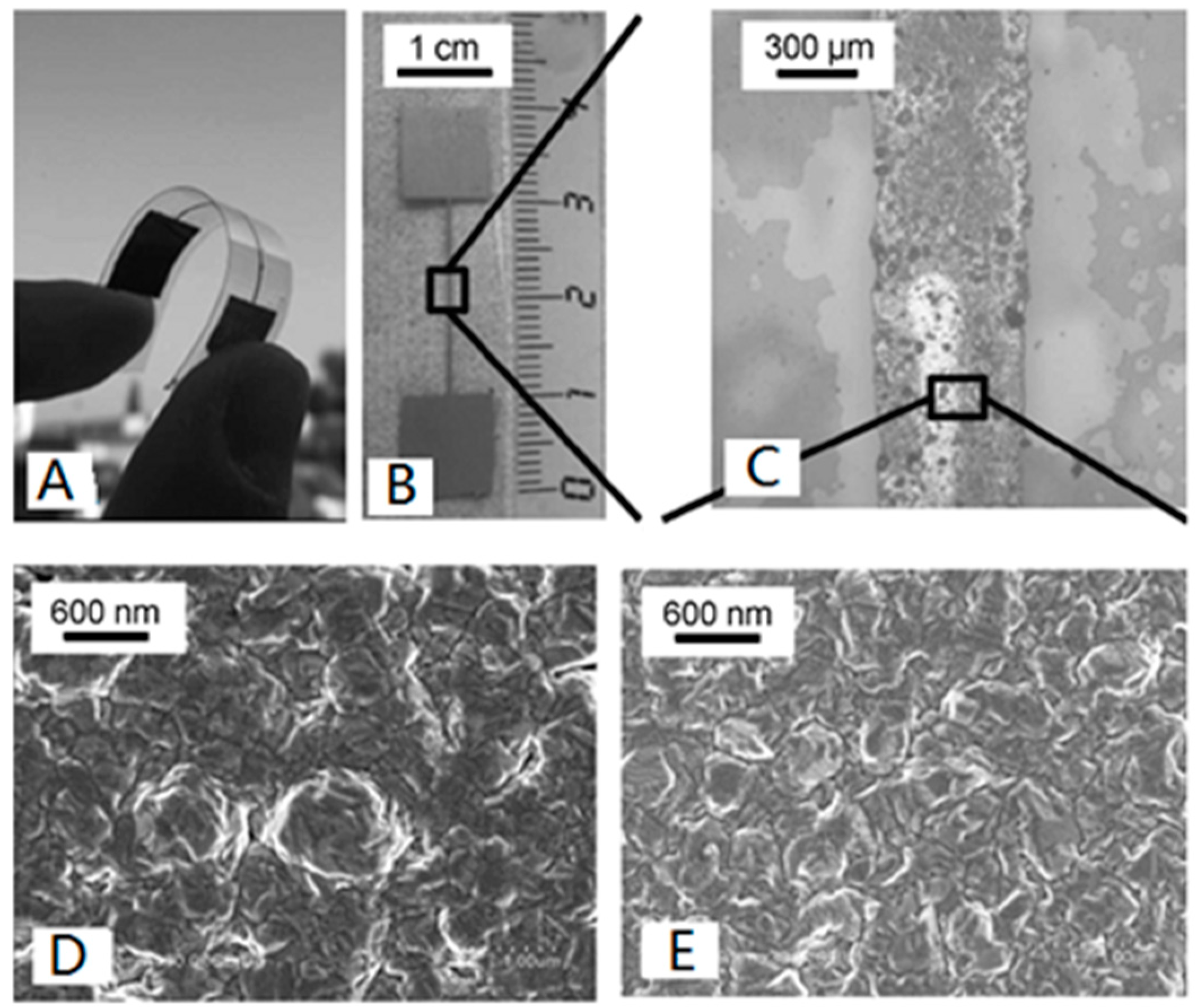
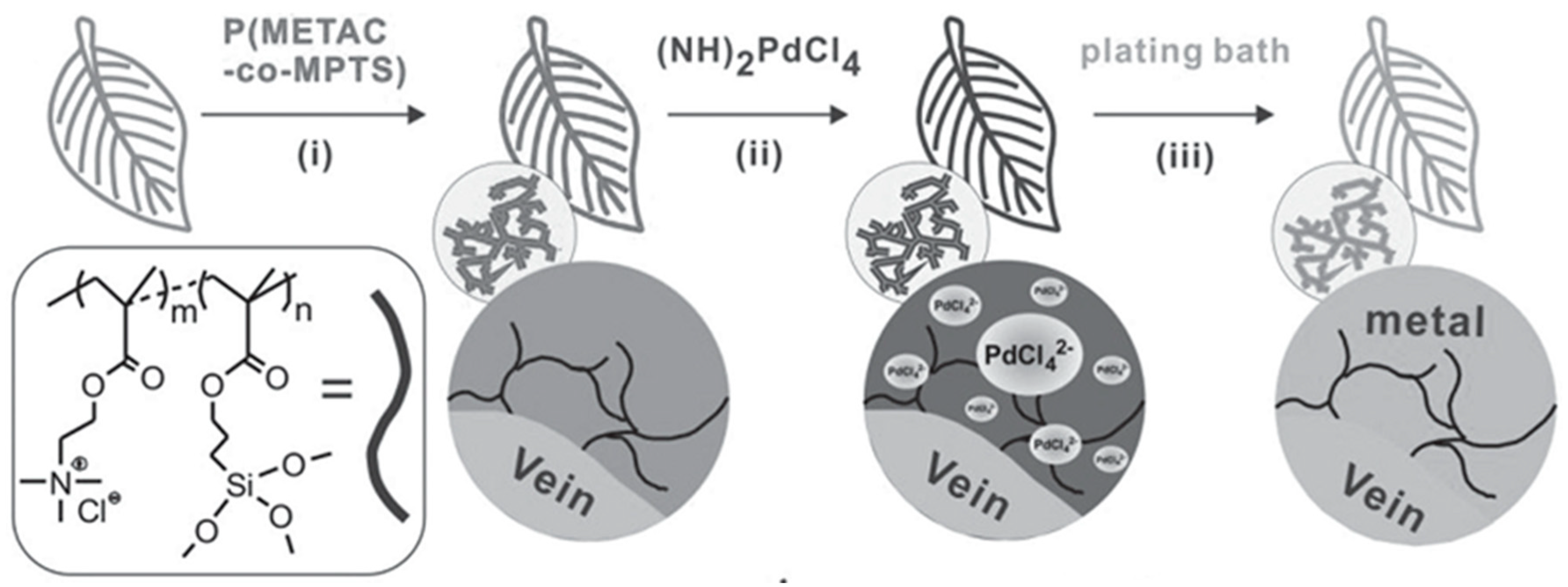
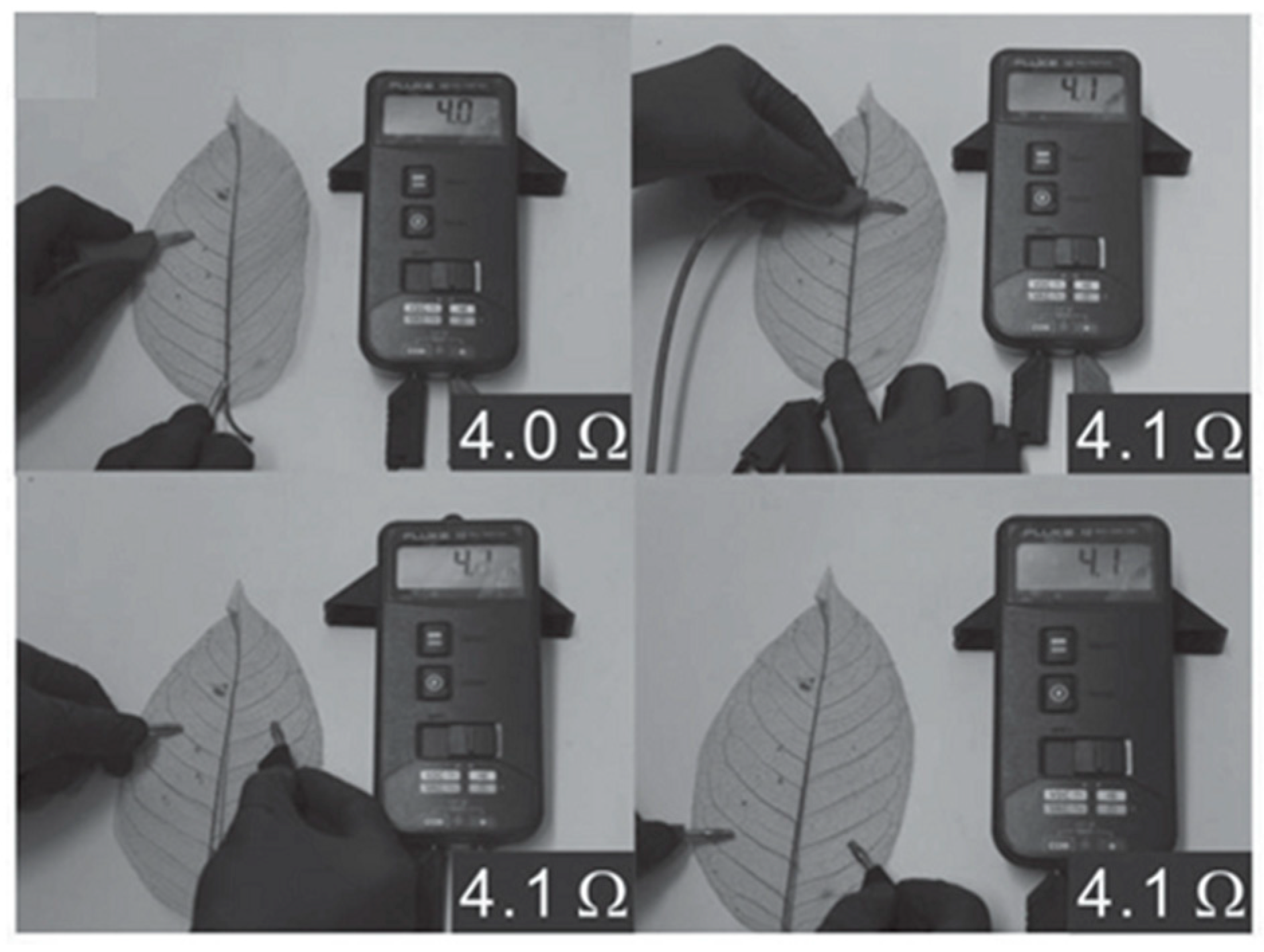
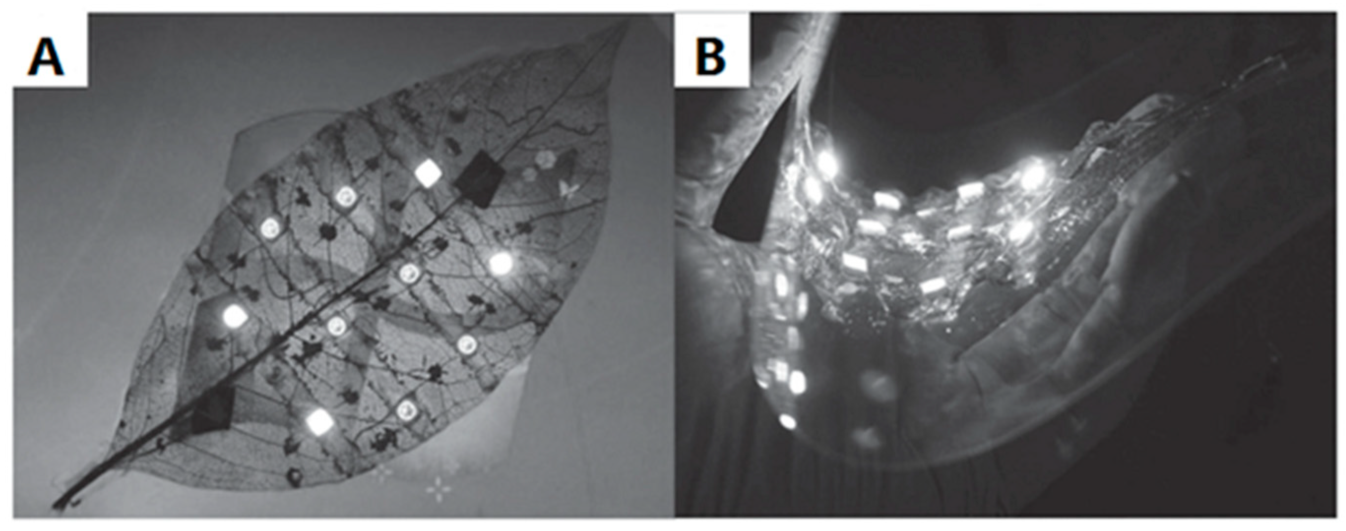
Nowadays, the ELD field tends to choose some bionic materials as an omnidirectional substrate, because natural fibres are green and cheap [10,25]. For instance, soft and stretchable plant leaves are suitable to act as substrates to be coated with a layer of metals by ELD. Recently, Zheng et al. [10] reported a method to fabricate vein-based transparent electrodes. A type of copolymer, P(METAC-co-MPTS), first modified the surfaces of natural veins; then these leaves, modified with polymer matrix, were immersed in a solution of (NH4)2PdCl4 for 2 h, after which [PdCl4]2− ions were captured for subsequent depositing. Finally, copper particles were deposited on the surface of vein substrates with the help of the plating bath (Figure 15). The electrode that was produced has excellent electrically conductive attributes and is nearly transparent. As Figure 16 shows, measuring different parts of the vein conductor reveals that resistances of thread conductor bulks are about 4 Ω, which is superior to some trading products. Also, when different strains were applied to the vein-based conductor and integrated with the LED, it could still, as a powering electronic device, work in the circuit (Figure 17).
3.5. ELD on Three-Dimensional Substrates
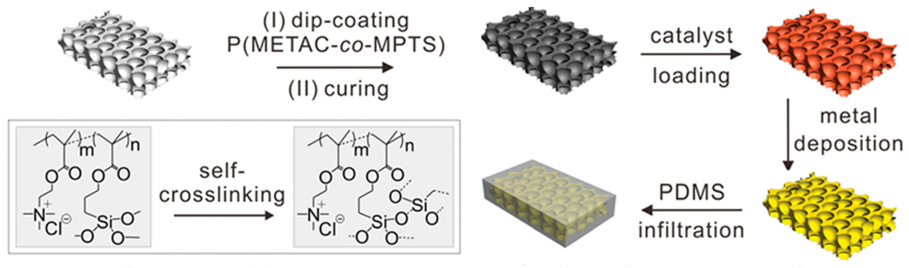
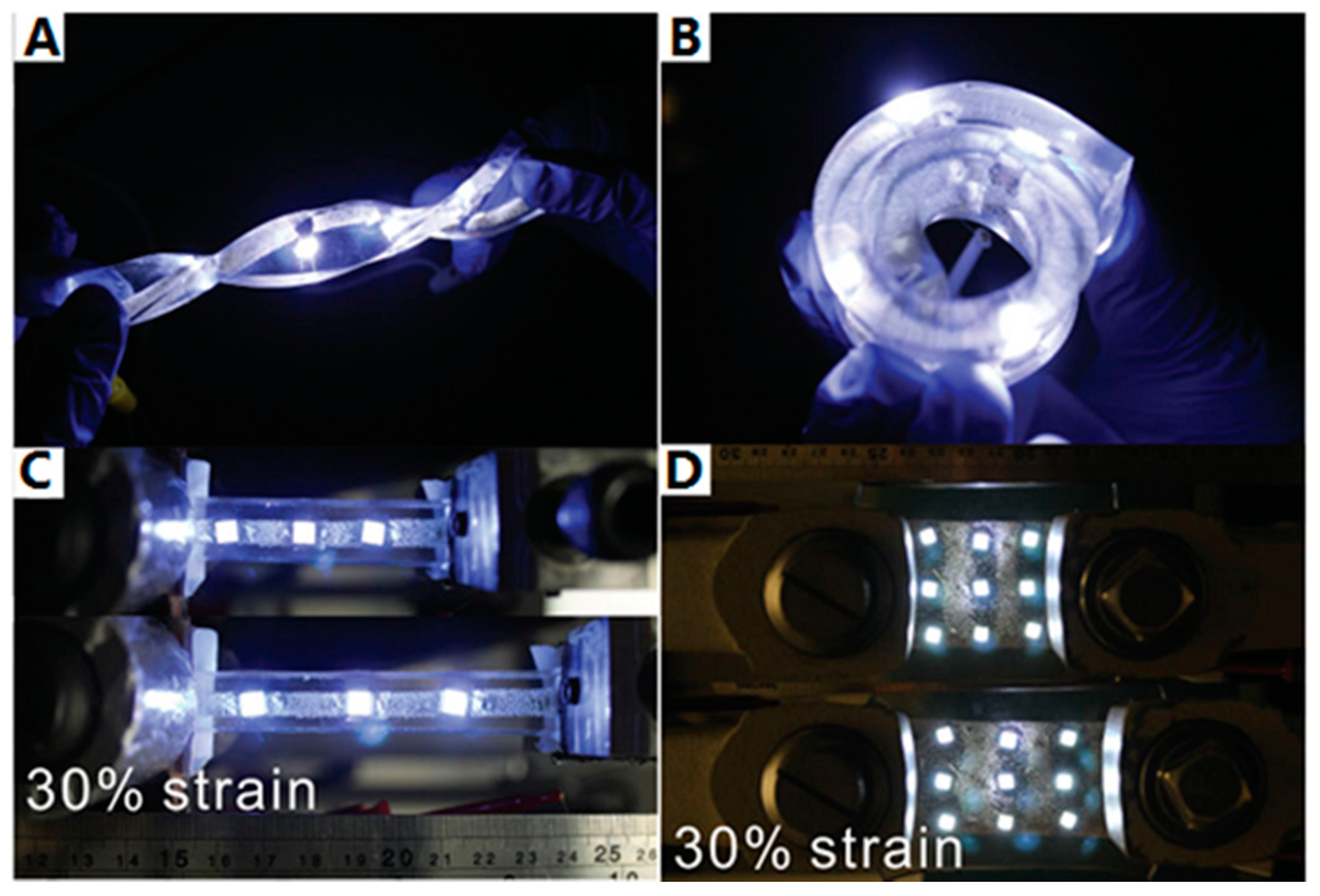
In previous reports, the PIME catalytic ELD only used two-dimensional conductors; however, Yu et al. [39] have introduced a new method to fabricate a flexible and stretchable three-dimensional wire on a porous polyurethane (PU) sponge. Unlike direct polymerisation on the substrate surface, the copolymer P(METAC-co-MPTS) was grafted by a dip coating and curing process. This approach can be roughly divided into three steps (Figure 18). (1) Bulk substrates were first dipped into an ethanol solution of P(METAC-co-MPTS) in the air-dried condition with bubbling of nitrogen gas; during the curing process, a connected layer formed by silane groups in the MPTS blocks built a robust adhesion between the polymer matrix and the PU sponges. (2) After immersing the surface-modified sponges in the catalyst solution, [PdCl4]2− ions were immobilised by PMETAC blocks. (3) A thin layer of metal film (copper, copper/silver, gold) was generated on the surface of the PU sponges by ELD in the plating bath. The three-dimensional electrodes that were produced presented conductive, flexible and durable properties. The main advantage is that 3D structures can protect the conductive surface from damage more effectively than two-dimensional ones, which could be proved by a 3D-network conductive pathway [39]. Figure 19 and Figure 20 show that resistance did not change significantly after polishing with abrasive paper or cutting in half by a razor blade.
4. Surface Lithography by PIME Catalytic ELD
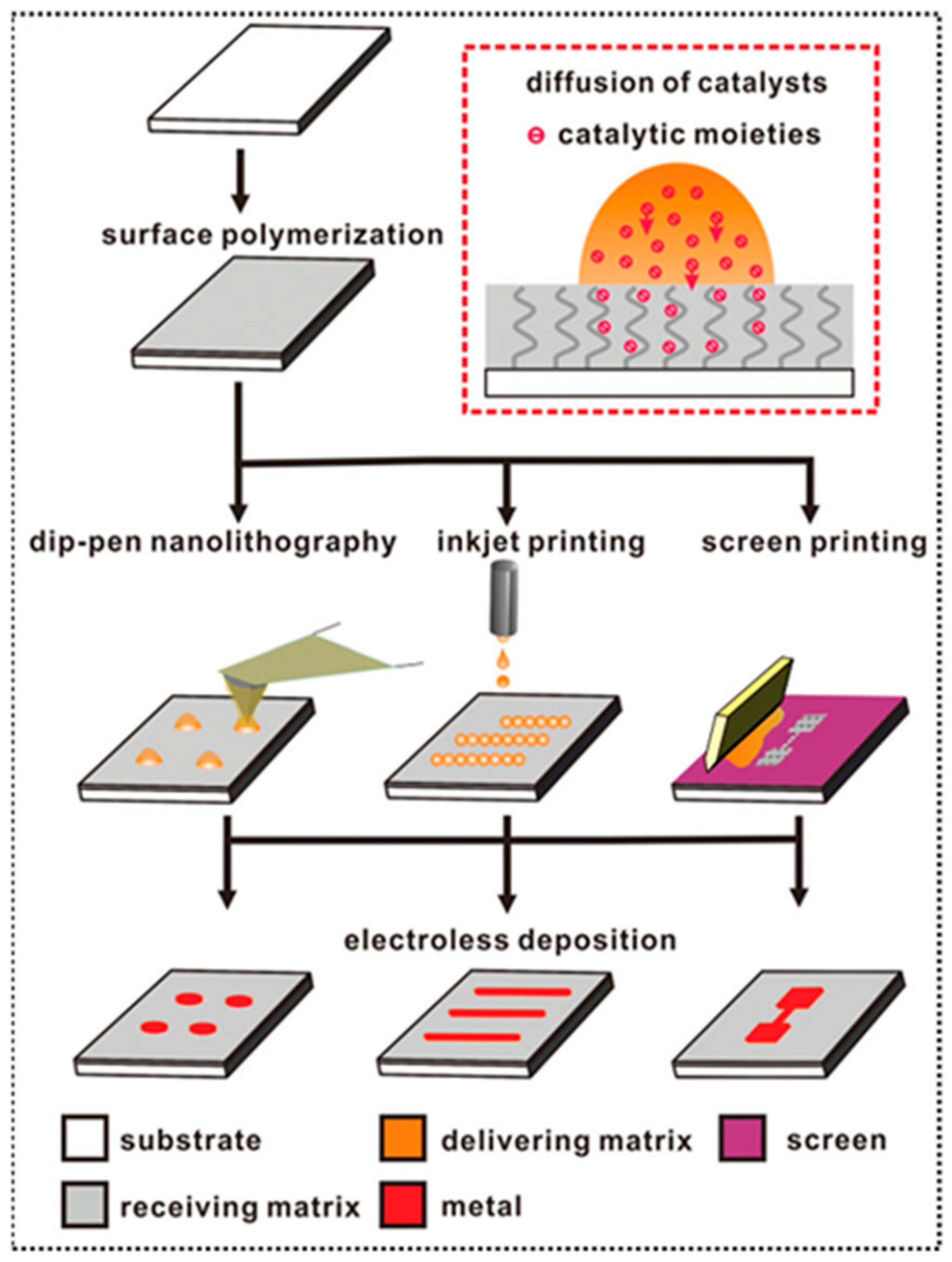
The most popular catalytic moieties for the PIME catalytic ELD technique are metal ions or nanoparticles [9]. The two most common methods for loading these catalytic moieties are immersing the substrates with polymer-modified surfaces into a metal-based salts solution, and printing the ink containing catalytic metal ions onto the modified surfaces. Although the first method is widely applied in many reports, printing techniques still play a fairly significant role in producing ELD wearable devices, because of their low cost and simplicity. Accordingly, it is important to identify advanced printing approaches through which cheap and high performance flexible ELD conductors can be fabricated. Nevertheless, due to the limitation of the viscosity problem of catalyst ink, inkjet printing has only been applied in ELD patterning techniques; this has a negative influence on producing variety and efficiency. In order to find new printing methods to coat metal layers, an effective way should be found to solve the problem of low ink viscosity.
Zheng et al. researched a novel approach to control the viscosity of the catalyst ink, by adding polyethylene glycol (PEG) as the delivering matrix [27]. In their report, the matrix-assisted catalytic printing (MACP) method was able to fabricate four metal conductors (copper, nickel, silver and gold) into different flexible substrates. The catalytic moieties were printed onto the substrate surface through three printing techniques—dip-pen nanolithography (DPN), inkjet printing and screen printing—rather than through immersing substrates directly in the catalyst solution or traditional lithography printing. As shown in Figure 21, PMETAC, which worked as a receiving platform, was grafted onto the substrate surface. The ink containing the catalyst solution and delivering matrix was then printed by three different printing methods. After ELD, the metal thin films formed on the printed areas. This method exhibited great selectivity and stability when transferring patterns from the ink to the metal layer.
The delivering matrix (PEG) played a vital role in these printing techniques [9,27]. The viscosity of the ink could be controlled effectively by the amount of PEG. For screen printing, the catalyst ink should be much more viscous than for dip-pen nanolithography (DPN) and inkjet printing. On the other hand, the water-absorbing PEG kept the ink’s moisture levels high to ensure that PMETAC had sufficient time to capture [PdCl4]2− ions during the process of diffusion. Therefore, the ELD of metal films could be fabricated through various printing approaches. In addition, these flexible and stretchable conductors illustrated good mechanical properties and stable electrical properties. The minimum resistivity of the four conductors (copper) was just 4.9 µΩ·cm [27].
5. Conclusions
PIME catalytic ELD is a versatile and efficient way of fabricating metal nanoparticles or thin films onto substrates to produce flexible and stretchable electronics. Generally, this low-cost, convenient technique contains three steps to achieve metal conductors: Modifying substrates with polymer interfaces; capturing catalytic moieties on the polymer-grafted areas; and subsequently depositing the metal layer in an ELD bath. The substrates applied for ELD can be chosen from a wide range of materials, such as plastics, elastomers, cotton, PET, three-dimensional sponges and even natural leaves. Some previously reported substrates, polymer interfaces and polymerisation methods employed for PIME catalytic ELD, are summarised in Table 1.
The polymer interface is an important part of the whole process of fabrication because interpenetrating networks are formed between the polymer matrices layer and metal nanoparticles. More significantly, this interpenetration provides a powerful adhesion to overcome mechanical failures and instability, which minimises the cracking of the metal layer from the substrate surface when the conductors are stretched or folded. At the same time, the metal films fabricated from PIME catalytic ELD are usually high performance, with excellent conductive properties. In addition, as well as traditional lithographic approaches [66,67,68,69,70,71,72,73,74,75] (including photolithography, scanning probe lithography and contact printing), some advanced printing techniques have been applied in the ELD field. These effective printing methods, such as dip-pen nanolithography, inkjet printing and screen printing, have the potential to improve the throughput of patterned ELD flexible electronics.
However, research about PIME catalytic ELD remains at a preliminary stage [4,9]. Several drawbacks such as long reaction time and tedious synthesis steps of surface polymerization limit the industrial scaling up productions, and hinder practical applications. Setting up a novel polymeric system by surface molecular engineering, should be conducted in future. Moreover, main research works focus on conductive metal nanoparticles deposition. Other functional materials, such as semi-conductors, cannot be coated by PIME catalytic ELD. The deposition process is conducted in an aqueous solution; water pollution and sustainable development should be conceived as a critical factor. Additionally, in current reports, most ELD metal structures are only applied as simple conductive wires and electrodes. Developing high performance e-textiles, or conductive patterns using PIME, should start under multidisciplinary collaboration. More applications, such as robotic skins, point-of-care diagnostics, wearable displays and biological actuators, should be conducted in future.
Author Contributions
X.L., Y.L. designed the structure of review and wrote the framework; C.Z. wrote the paper and C.Z. and X.L. finalized the paper.
Acknowledgments
We would like to thank the support of the EU Horizon 2020 and University of Manchester through projects with project codes 644268-ETEXWELD-H2020-MSCA-RISE-2014, AA14512 (UMRI project “Graphene-Smart Textiles E-Healthcare Network”) and the British Cotton Growing Association Work People’s Collection Fund for funding the project “Protective Efficiency of Respiratory Protective Equipment (RPE) against Byssinosis for Cotton Workers’’.
Conflicts of Interest
The authors declare no conflict of interest.
References
- Benight, S.J.; Wang, C.; Tok, J.B.; Bao, Z. Stretchable and self-healing polymers and devices for electronic skin. Prog. Polym. Sci. 2013, 38, 1961–1977. [Google Scholar] [CrossRef]
- Hu, L.; Pasta, M.; La Mantia, F.; Cui, L.; Jeong, S.; Deshazer, H.D.; Choi, J.W.; Han, S.M.; Cui, Y. Stretchable, porous, and conductive energy textiles. Nano Lett. 2010, 10, 708–714. [Google Scholar] [CrossRef] [PubMed]
- Kim, D.-H.; Lu, N.; Ma, R.; Kim, Y.-S.; Kim, R.-H.; Wang, S.; Wu, J.; Won, S.M.; Tao, H.; Islam, A. Epidermal electronics. Science 2011, 333, 838–843. [Google Scholar] [CrossRef] [PubMed]
- Liu, X.; Zhou, X.; Li, Y.; Zheng, Z. Surface-Grafted Polymer-Assisted Electroless Deposition of Metals for Flexible and Stretchable Electronics. Chemistry 2012, 7, 862–870. [Google Scholar] [CrossRef] [PubMed]
- Shang, S.; Zeng, W.; Tao, X.-M. High stretchable MWNTs/polyurethane conductive nanocomposites. J. Mater. Chem. 2011, 21, 7274–7280. [Google Scholar] [CrossRef]
- Webb, R.C.; Bonifas, A.P.; Behnaz, A.; Zhang, Y.; Yu, K.J.; Cheng, H.; Shi, M.; Bian, Z.; Liu, Z.; Kim, Y.-S. Ultrathin conformal devices for precise and continuous thermal characterization of human skin. Nat. Mater. 2013, 12, 938–944. [Google Scholar] [CrossRef] [PubMed]
- White, M.S.; Kaltenbrunner, M.; Głowacki, E.D.; Gutnichenko, K.; Kettlgruber, G.; Graz, I.; Aazou, S.; Ulbricht, C.; Egbe, D.A.; Miron, M.C. Ultrathin, highly flexible and stretchable PLEDs. Nat. Photonics 2013, 7, 811–816. [Google Scholar] [CrossRef]
- Yeo, W.H.; Kim, Y.S.; Lee, J.; Ameen, A.; Shi, L.; Li, M.; Wang, S.; Ma, R.; Jin, S.H.; Kang, Z. Multifunctional epidermal electronics printed directly onto the skin. Adv. Mater. 2013, 25, 2773–2778. [Google Scholar] [CrossRef] [PubMed]
- Yu, Y.; Yan, C.; Zheng, Z. Polymer-Assisted Metal Deposition (PAMD): A Full-Solution Strategy for Flexible, Stretchable, Compressible, and Wearable Metal Conductors. Adv. Mater. 2014, 26, 5508–5516. [Google Scholar] [CrossRef] [PubMed]
- Yu, Y.; Zhang, Y.; Li, K.; Yan, C.; Zheng, Z. Bio-Inspired Chemical Fabrication of Stretchable Transparent Electrodes. Small 2015, 11, 3444–3449. [Google Scholar] [CrossRef] [PubMed]
- An, B.W.; Shin, J.H.; Kim, S.-Y.; Kim, J.; Ji, S.; Park, J.; Lee, Y.; Jang, J.; Park, Y.-G.; Cho, E. Smart Sensor Systems for Wearable Electronic Devices. Polymers 2017, 9, 303. [Google Scholar] [CrossRef]
- Genc, R.; Alas, M.O.; Harputlu, E.; Repp, S.; Kremer, N.; Castellano, M.; Colak, S.G.; Ocakoglu, K.; Erdem, E. High-Capacitance Hybrid Supercapacitor Based on Multi-Colored Fluorescent Carbon-Dots. Sci. Rep. 2017, 7, 11222. [Google Scholar] [CrossRef] [PubMed]
- Repp, S.; Harputlu, E.; Gurgen, S.; Castellano, M.; Kremer, N.; Pompe, N.; Wörner, J.; Hoffmann, A.; Thomann, R.; Emen, F.M. Synergetic effects of Fe3+ doped spinel Li4Ti5O12 nanoparticles on reduced graphene oxide for high surface electrode hybrid supercapacitors. Nanoscale 2018, 10, 1877–1884. [Google Scholar] [CrossRef] [PubMed]
- Lehtimäki, S.; Suominen, M.; Damlin, P.; Tuukkanen, S.; Kvarnström, C.; Lupo, D. Preparation of supercapacitors on flexible substrates with electrodeposited PEDOT/graphene composites. ACS Appl. Mater. Interfaces 2015, 7, 22137–22147. [Google Scholar] [CrossRef] [PubMed]
- Haddara, Y.M.; Howlader, M.M. Integration of Heterogeneous Materials for Wearable Sensors. Polymers 2018, 10, 60. [Google Scholar] [CrossRef]
- Silva, R.; Franchi, D.; Leone, A.; Pilloni, L.; Masci, A.; Pozio, A. Surface conductivity and stability of metallic bipolar plate materials for polymer electrolyte fuel cells. Electrochim. Acta 2006, 51, 3592–3598. [Google Scholar] [CrossRef]
- Limb, S.J.; Gleason, K.K.; Edell, D.J.; Gleason, E.F. Flexible fluorocarbon wire coatings by pulsed plasma enhanced chemical vapor deposition. J. Vac. Sci. Technol. A 1997, 15, 1814–1818. [Google Scholar] [CrossRef]
- Sun, Y.; Rogers, J.A. Inorganic semiconductors for flexible electronics. Adv. Mater. 2007, 19, 1897–1916. [Google Scholar] [CrossRef]
- Geiser, J. Multiscale modeling of chemical vapor deposition (CVD) apparatus: Simulations and approximations. Polymers 2013, 5, 142–160. [Google Scholar] [CrossRef]
- Brosteaux, D.; Axisa, F.; Gonzalez, M.; Vanfleteren, J. Design and fabrication of elastic interconnections for stretchable electronic circuits. IEEE Electron Device Lett. 2007, 28, 552–554. [Google Scholar] [CrossRef]
- Cho, S.; Kim, S.; Lee, J.; Lee, N.-E. Micro-scale metallization of high aspect-ratio Cu and Au lines on flexible polyimide substrate by electroplating using SU-8 photoresist mask. Microelectron. Eng. 2005, 77, 116–124. [Google Scholar] [CrossRef]
- Li, X.; Pei, W.; Tang, R.; Gui, Q.; Guo, K.; Wang, Y.; Chen, H. Investigation of flexible electrodes modified by TiN, Pt black and IrO x. Sci. China Technol. Sci. 2011, 54, 2305–2309. [Google Scholar] [CrossRef]
- Cheng, K.; Yang, M.H.; Chiu, W.W.; Huang, C.Y.; Chang, J.; Ying, T.F.; Yang, Y. Ink-Jet Printing, Self-Assembled Polyelectrolytes, and Electroless Plating: Low Cost Fabrication of Circuits on a Flexible Substrate at Room Temperature. Macromol. Rapid Commun. 2005, 26, 247–264. [Google Scholar] [CrossRef]
- Zschieschang, U.; Klauk, H.; Halik, M.; Schmid, G.; Dehm, C. Flexible organic circuits with printed gate electrodes. Adv. Mater. 2003, 15, 1147–1151. [Google Scholar] [CrossRef]
- Guo, R.; Yu, Y.; Zeng, J.; Liu, X.; Zhou, X.; Niu, L.; Gao, T.; Li, K.; Yang, Y.; Zhou, F. Biomimicking Topographic Elastomeric Petals (E-Petals) for Omnidirectional Stretchable and Printable Electronics. Adv. Sci. 2015, 2. [Google Scholar] [CrossRef] [PubMed]
- Liu, L.; Yu, Y.; Yan, C.; Li, K.; Zheng, Z. Wearable energy-dense and power-dense supercapacitor yarns enabled by scalable graphene-metallic textile composite electrodes. Nat. Commun. 2015, 6, 7260. [Google Scholar] [CrossRef] [PubMed]
- Guo, R.; Yu, Y.; Xie, Z.; Liu, X.; Zhou, X.; Gao, Y.; Liu, Z.; Zhou, F.; Yang, Y.; Zheng, Z. Matrix-Assisted Catalytic Printing for the Fabrication of Multiscale, Flexible, Foldable, and Stretchable Metal Conductors. Adv. Mater. 2013, 25, 3343–3350. [Google Scholar] [CrossRef] [PubMed]
- Edmondson, S.; Osborne, V.L.; Huck, W.T. Polymer brushes via surface-initiated polymerizations. Chem. Soc. Rev. 2004, 33, 14–22. [Google Scholar] [CrossRef] [PubMed]
- Pyun, J.; Kowalewski, T.; Matyjaszewski, K. Synthesis of polymer brushes using atom transfer radical polymerization. Macromol. Rapid Commun. 2003, 24, 1043–1059. [Google Scholar] [CrossRef]
- Deng, J.; Wang, L.; Liu, L.; Yang, W. Developments and new applications of UV-induced surface graft polymerizations. Prog. Polym. Sci. 2009, 34, 156–193. [Google Scholar] [CrossRef]
- Kang, E.T.; Zhang, Y. Surface modification of fluoropolymers via molecular design. Adv. Mater. 2000, 12, 1481–1494. [Google Scholar] [CrossRef]
- Nasef, M.M.; Hegazy, E.-S.A. Preparation and applications of ion exchange membranes by radiation-induced graft copolymerization of polar monomers onto non-polar films. Prog. Polym. Sci. 2004, 29, 499–561. [Google Scholar] [CrossRef] [Green Version]
- Lee, H.; Dellatore, S.M.; Miller, W.M.; Messersmith, P.B. Mussel-inspired surface chemistry for multifunctional coatings. Science 2007, 318, 426–430. [Google Scholar] [CrossRef] [PubMed]
- Li, D.; Shen, H.; Cai, C.; Sun, T.; Zhao, Y.; Chen, L.; Zhao, N.; Xu, J. Fabrication of Conductive Silver Microtubes Using Natural Catkin as a Template. ACS Omega 2017, 2, 1738–1745. [Google Scholar] [CrossRef]
- Azzaroni, O.; Zheng, Z.; Yang, Z.; Huck, W.T. Polyelectrolyte brushes as efficient ultrathin platforms for site-selective copper electroless deposition. Langmuir 2006, 22, 6730–6733. [Google Scholar] [CrossRef] [PubMed]
- Liu, X.; Li, Y.; Zheng, Z. Programming nanostructures of polymer brushes by dip-pen nanodisplacement lithography (DNL). Nanoscale 2010, 2, 2614–2618. [Google Scholar] [CrossRef] [PubMed]
- Wang, X.; Hu, H.; Shen, Y.; Zhou, X.; Zheng, Z. Stretchable conductors with ultrahigh tensile strain and stable metallic conductance enabled by prestrained polyelectrolyte nanoplatforms. Adv. Mater. 2011, 23, 3090–3094. [Google Scholar] [CrossRef] [PubMed]
- Wang, X.; Zhang, T.; Kobe, B.; Lau, W.M.; Yang, J. Grafting of polyelectrolytes onto hydrocarbon surfaces by high-energy hydrogen induced cross-linking for making metallized polymer films. Chem. Commun. 2013, 49, 4658–4660. [Google Scholar] [CrossRef] [PubMed]
- Yu, Y.; Zeng, J.; Chen, C.; Xie, Z.; Guo, R.; Liu, Z.; Zhou, X.; Yang, Y.; Zheng, Z. Three-Dimensional Compressible and Stretchable Conductive Composites. Adv. Mater. 2014, 26, 810–815. [Google Scholar] [CrossRef] [PubMed]
- Garcia, A.; Berthelot, T.; Viel, P.; Polesel-Maris, J.; Palacin, S. Microscopic study of a ligand induced electroless plating process onto polymers. ACS Appl. Mater. Interfaces 2010, 2, 3043–3051. [Google Scholar] [CrossRef] [PubMed]
- Garcia, A.; Hanifi, N.; Jousselme, B.; Jégou, P.; Palacin, S.; Viel, P.; Berthelot, T. Polymer grafting by inkjet printing: A direct chemical writing toolset. Adv. Funct. Mater. 2013, 23, 3668–3674. [Google Scholar] [CrossRef]
- Lancaster, J.R.; Jehani, J.; Carroll, G.T.; Chen, Y.; Turro, N.J.; Koberstein, J.T. Toward a universal method to pattern metals on a polymer. Chem. Mater. 2008, 20, 6583–6585. [Google Scholar] [CrossRef]
- Liu, X.; Guo, R.; Shi, Y.; Deng, L.; Li, Y. Durable, Washable, and Flexible Conductive PET Fabrics Designed by Fiber Interfacial Molecular Engineering. Macromol. Mater. Eng. 2016, 301, 1383–1389. [Google Scholar] [CrossRef]
- Garcia, A.; Berthelot, T.; Viel, P.; Mesnage, A.; Jégou, P.; Nekelson, F.; Roussel, S.; Palacin, S. ABS polymer electroless plating through a one-step poly (acrylic acid) covalent grafting. ACS Appl. Mater. Interfaces 2010, 2, 1177–1183. [Google Scholar] [CrossRef] [PubMed]
- Garcia, A.; Polesel-Maris, J.; Viel, P.; Palacin, S.; Berthelot, T. Localized ligand induced electroless plating (LIEP) process for the fabrication of copper patterns onto flexible polymer substrates. Adv. Funct. Mater. 2011, 21, 2096–2102. [Google Scholar] [CrossRef]
- Mévellec, V.; Roussel, S.; Tessier, L.; Chancolon, J.; Mayne-L’Hermite, M.; Deniau, G.; Viel, P.; Palacin, S. Grafting polymers on surfaces: A new powerful and versatile diazonium salt-based one-step process in aqueous media. Chem. Mater. 2007, 19, 6323–6330. [Google Scholar] [CrossRef]
- Liu, Z.; Hu, H.; Yu, B.; Chen, M.; Zheng, Z.; Zhou, F. Binary oppositely charged polyelectrolyte brushes for highly selective electroless deposition of bimetallic patterns. Electrochem. Commun. 2009, 11, 492–495. [Google Scholar] [CrossRef]
- Chen, Y.; Kang, E.; Neoh, K.; Huang, W. Electroless metallization of glass surfaces functionalized by silanization and graft polymerization of aniline. Langmuir 2001, 17, 7425–7432. [Google Scholar] [CrossRef]
- Ma, Z.; Tan, K.; Alian, A.D.; Kang, E.; Neoh, K. Electroless plating of copper on poly (tetrafluoroethylene) films modified by NH3 plasma and surface graft copolymerization with aniline. J. Vac. Sci. Technol. A 2001, 19, 2471–2478. [Google Scholar] [CrossRef]
- Wu, S.; Kang, E.; Neoh, K.; Tan, K. Electroless deposition of copper on surface modified poly (tetrafluoroethylene) films from graft copolymerization and silanization. Langmuir 2000, 16, 5192–5198. [Google Scholar] [CrossRef]
- Yu, Z.; Kang, E.; Neoh, K. Amidoximation of the acrylonitrile polymer grafted on poly (tetrafluoroethylene-co-hexafluoropropylene) films and its relevance to the electroless plating of copper. Langmuir 2002, 18, 10221–10230. [Google Scholar] [CrossRef]
- Hao, Z.; Chen, H.; Ma, D. Preparation of micro gold devices on poly (dimethylsiloxane) chips with region-selective electroless plating. Anal. Chem. 2009, 81, 8649–8653. [Google Scholar] [CrossRef] [PubMed]
- Wang, W.; Li, R.; Tian, M.; Liu, L.; Zou, H.; Zhao, X.; Zhang, L. Surface silverized meta-aramid fibers prepared by bio-inspired poly (dopamine) functionalization. ACS Appl. Mater. Interfaces 2013, 5, 2062–2069. [Google Scholar] [CrossRef] [PubMed]
- Liu, X.; Chang, H.; Li, Y.; Huck, W.T.; Zheng, Z. Polyelectrolyte-bridged metal/cotton hierarchical structures for highly durable conductive yarns. ACS Appl. Mater. Interfaces 2010, 2, 529–535. [Google Scholar] [CrossRef] [PubMed]
- Sekitani, T.; Someya, T. Stretchable, large-area organic electronics. Adv. Mater. 2010, 22, 2228–2246. [Google Scholar] [CrossRef] [PubMed]
- Ali, A.E.H.; Aal, A.A. Conductive thin film formation onto radiation grafted polymeric surfaces using electroless plating technique. Polym. Adv. Technol. 2009, 20, 729–735. [Google Scholar] [CrossRef]
- Li, L.; Yan, G.; Wu, J.; Yu, X.; Guo, Q.; Kang, E. Electroless plating of copper on polyimide films modified by surface-initiated atom-transfer radical polymerization of 4-vinylpyridine. Appl. Surf. Sci. 2008, 254, 7331–7335. [Google Scholar] [CrossRef]
- Wang, W.; Vora, R.; Kang, E.; Neoh, K. Electroless plating of copper on fluorinated polyimide films modified by surface graft copolymerization with 1-vinylimidazole and 4-vinylpyridine. Polym. Eng. Sci. 2004, 44, 362–375. [Google Scholar] [CrossRef]
- Wang, W.; Zhang, Y.; Kang, E.; Neoh, K. Electroless deposition of copper on poly (tetrafluoroethylene) films modified by plasma-induced surface grafting of poly (4-vinylpyridine). Plasmas Polym. 2002, 7, 207–225. [Google Scholar] [CrossRef]
- Wang, W.C.; Vora, R.K.H.; Kang, E.T.; Neoh, K.G. Electroless Plating of Copper on Fluorinated Polyimide Films Modified by Plasma Graft Copolymerization and UV-induced Graft Copolymerization with 4-Vinylpyridine. Macromol. Mater. Eng. 2003, 288, 152–163. [Google Scholar] [CrossRef]
- Wu, D.; Zhang, T.; Wang, W.C.; Zhang, L.; Jin, R. Reflective and conductive surface-silvered polyimide films prepared by surface graft copolymerization and electroless plating. Polym. Adv. Technol. 2008, 19, 335–341. [Google Scholar] [CrossRef]
- Yang, G.; Lim, C.; Tan, Y.; Zhang, Y.; Kang, E.; Neoh, K. Electroless deposition of nickel on fluoropolymers modified by surface graft copolymerization. Eur. Polym. J. 2002, 38, 2153–2160. [Google Scholar] [CrossRef]
- Yu, W.; Zhang, Y.; Kang, E.; Neoh, K.; Wu, S.; Chow, Y. Electroless plating of copper via a Sn-free process on dielectric SiLK surface modified by UV-induced graft copolymerization with 4-vinylpyridine and 1-vinylimidazole. J. Electrochem. Soc. 2002, 149, C521–C528. [Google Scholar] [CrossRef]
- Zhu, Y.; Kang, E.; Neoh, K.; Osipowicz, T.; Chan, L. Plasma graft copolymerization of 4-vinylpyridine on dense and porous SiLK for electroless plating of copper and for retardation of copper diffusion. J. Electrochem. Soc. 2005, 152, F107–F114. [Google Scholar] [CrossRef]
- Shojaei, A.; Fathi, R.; Sheikh, N. Adhesion modification of polyethylenes for metallization using radiation-induced grafting of vinyl monomers. Surf. Coat. Technol. 2007, 201, 7519–7529. [Google Scholar] [CrossRef]
- Gates, B.D.; Xu, Q.; Stewart, M.; Ryan, D.; Willson, C.G.; Whitesides, G.M. New approaches to nanofabrication: Molding, printing, and other techniques. Chem. Rev. 2005, 105, 1171–1196. [Google Scholar] [CrossRef] [PubMed]
- Ginger, D.S.; Zhang, H.; Mirkin, C.A. Zur Entwicklung der Dip-Pen-Nanolithographie. Angew. Chem. 2004, 116, 30–46. [Google Scholar] [CrossRef]
- Haq, E.U.; Liu, Z.; Zhang, Y.; Ahmad, S.A.A.; Wong, L.-S.; Armes, S.P.; Hobbs, J.K.; Leggett, G.J.; Micklefield, J.; Roberts, C.J. Parallel scanning near-field photolithography: The snomipede. Nano Lett. 2010, 10, 4375–4380. [Google Scholar] [CrossRef] [PubMed]
- Nie, Z.; Kumacheva, E. Patterning surfaces with functional polymers. Nat. Mater. 2008, 7, 277–290. [Google Scholar] [CrossRef] [PubMed]
- Zhou, X.; Boey, F.; Huo, F.; Huang, L.; Zhang, H. Chemically functionalized surface patterning. Small 2011, 7, 2273–2289. [Google Scholar] [CrossRef] [PubMed]
- Zhou, X.; Boey, F.; Zhang, H. Controlled growth of single-walled carbon nanotubes on patterned substrates. Chem. Soc. Rev. 2011, 40, 5221–5231. [Google Scholar] [CrossRef] [PubMed]
- Zhou, X.; Liu, X.; Xie, Z.; Zheng, Z. 3D-patterned polymer brush surfaces. Nanoscale 2011, 3, 4929–4939. [Google Scholar] [CrossRef]
- Zhou, X.; Wang, X.; Shen, Y.; Xie, Z.; Zheng, Z. Fabrication of Arbitrary Three-Dimensional Polymer Structures by Rational Control of the Spacing between Nanobrushes. Angew. Chem. Int. Ed. 2011, 50, 6506–6510. [Google Scholar] [CrossRef] [PubMed]
- Chandran, R.; Nowlin, K.; LaJeunesse, D.R. Nanosphere Lithography of Chitin and Chitosan with Colloidal and Self-Masking Patterning. Polymers 2018, 10, 218. [Google Scholar] [CrossRef]
- Nagato, K. Injection compression molding of replica molds for nanoimprint lithography. Polymers 2014, 6, 604–612. [Google Scholar] [CrossRef]
Figure 1.
The conventional process for PIME catalytic ELD [4].
Figure 1.
The conventional process for PIME catalytic ELD [4].
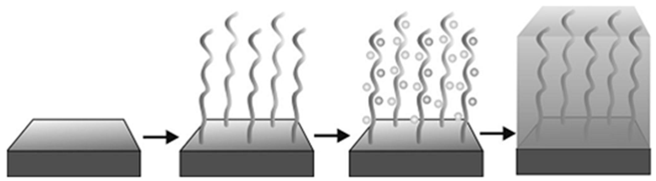
Figure 2.
An illustration of polymerisation methods of the PIME catalytic ELD: (a) SI ATRP is applied on a flexible substrate; (b) In situ, FRP is conducted in situ via various printing techniques; (c) self-crosslinking copolymerisation is used on a three-dimensional (3D) electronic structure [9].
Figure 2.
An illustration of polymerisation methods of the PIME catalytic ELD: (a) SI ATRP is applied on a flexible substrate; (b) In situ, FRP is conducted in situ via various printing techniques; (c) self-crosslinking copolymerisation is used on a three-dimensional (3D) electronic structure [9].
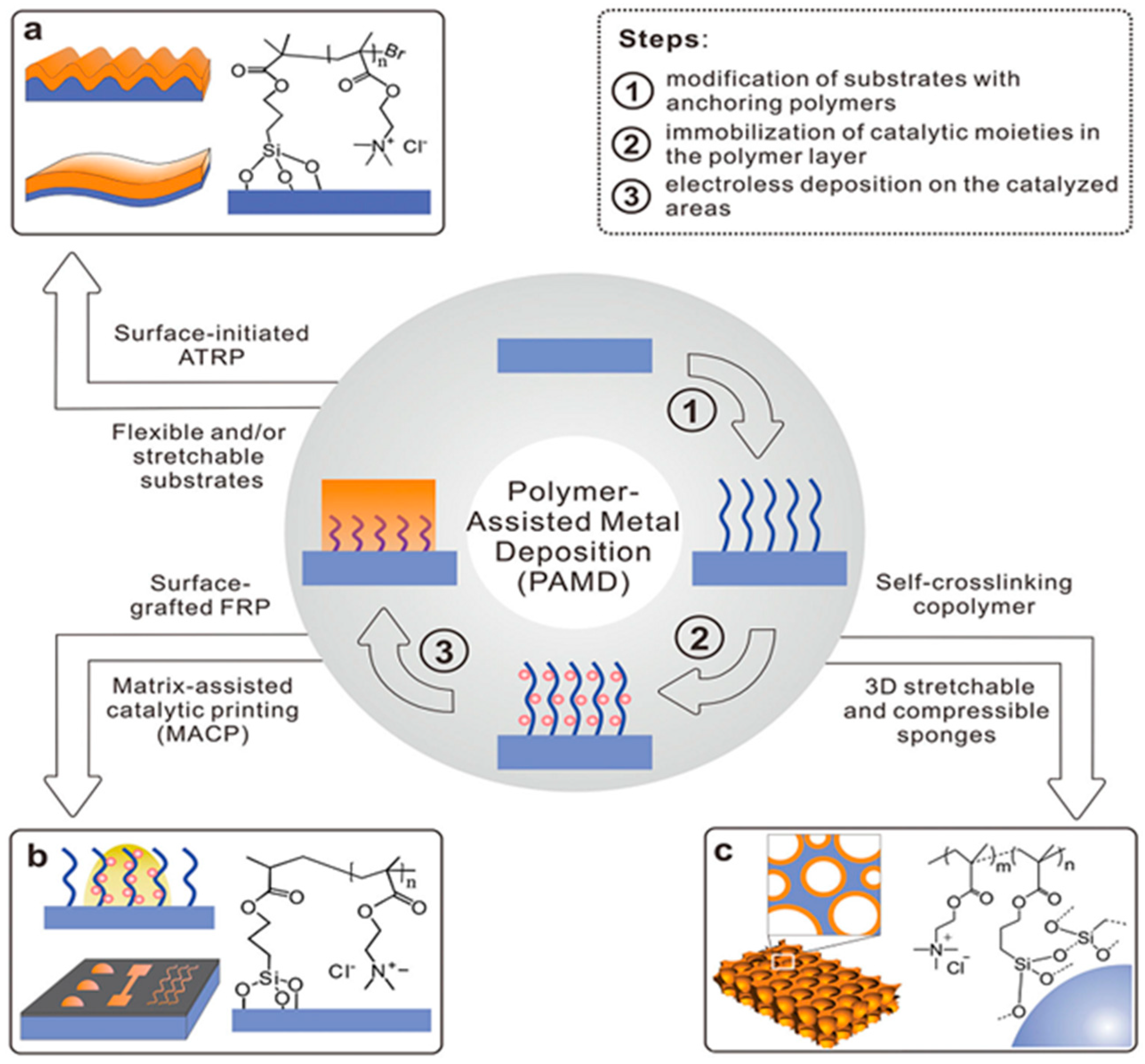
Figure 3.
An illustration of the process of PMETAC-assisted copper ELD on PET substrates [43].
Figure 3.
An illustration of the process of PMETAC-assisted copper ELD on PET substrates [43].
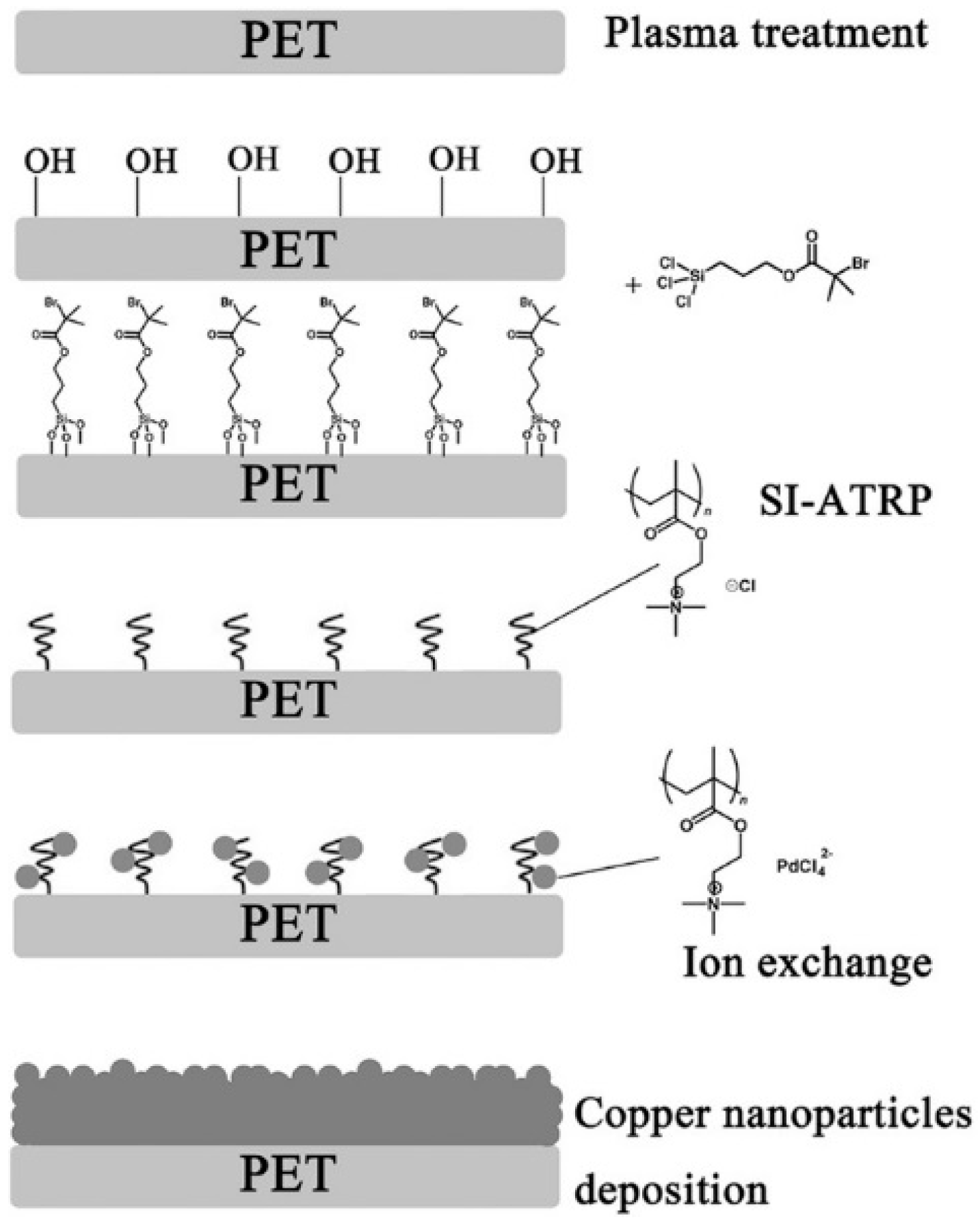
Figure 4.
The process of ELD with diblock polymer PS-b-PtBA: (A) the copolymer was grafted onto the PS substrate; (B) PtBA blocks were transferred into PAA blocks under UV-radiation; (C) the catalytic ions were anchored by PAA brushes; (D) metal thin films formed in the catalytic areas [42].
Figure 4.
The process of ELD with diblock polymer PS-b-PtBA: (A) the copolymer was grafted onto the PS substrate; (B) PtBA blocks were transferred into PAA blocks under UV-radiation; (C) the catalytic ions were anchored by PAA brushes; (D) metal thin films formed in the catalytic areas [42].
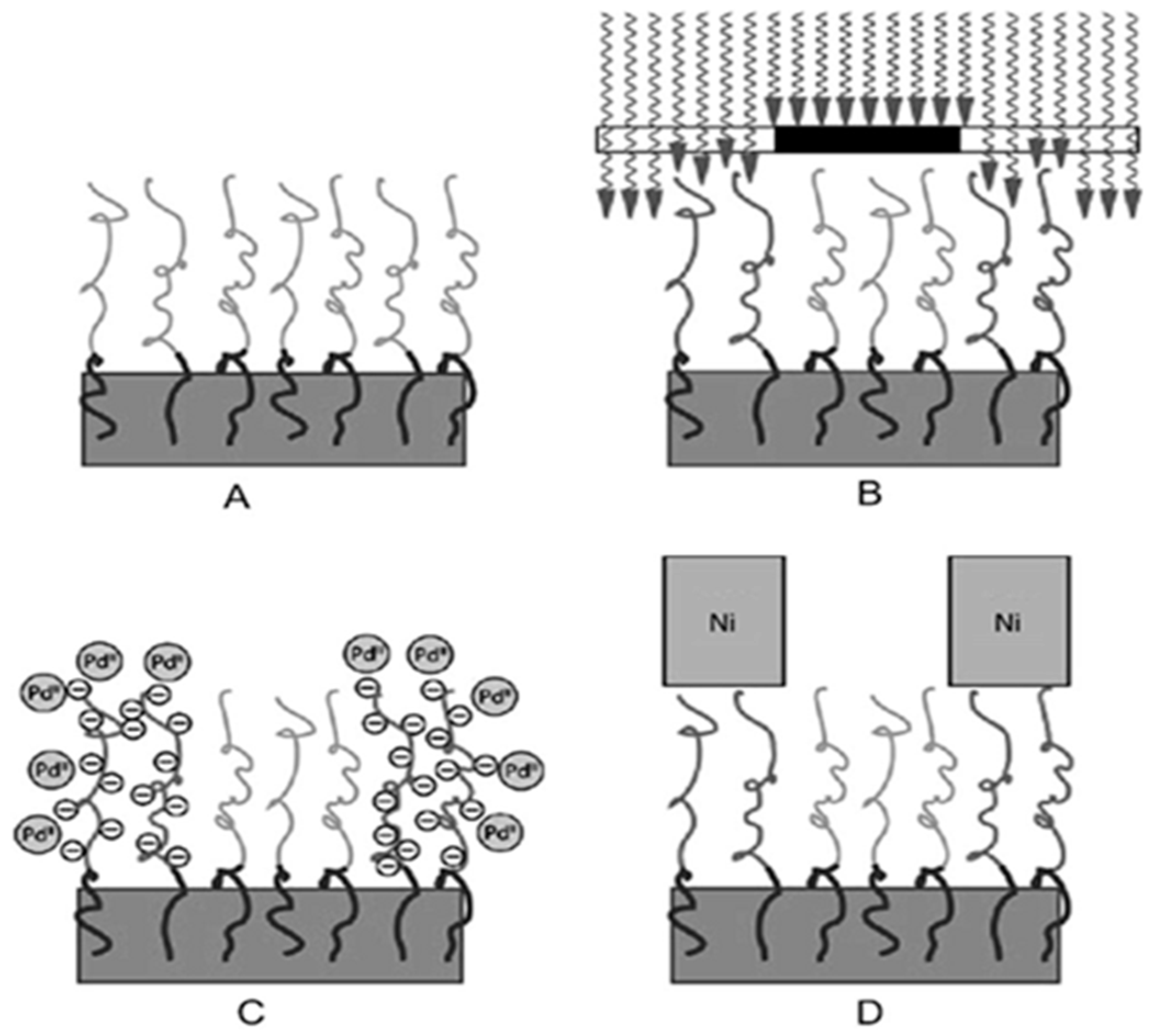
Figure 5.
The process of ligand-induced electroless plating (LIEP) [40].
Figure 5.
The process of ligand-induced electroless plating (LIEP) [40].
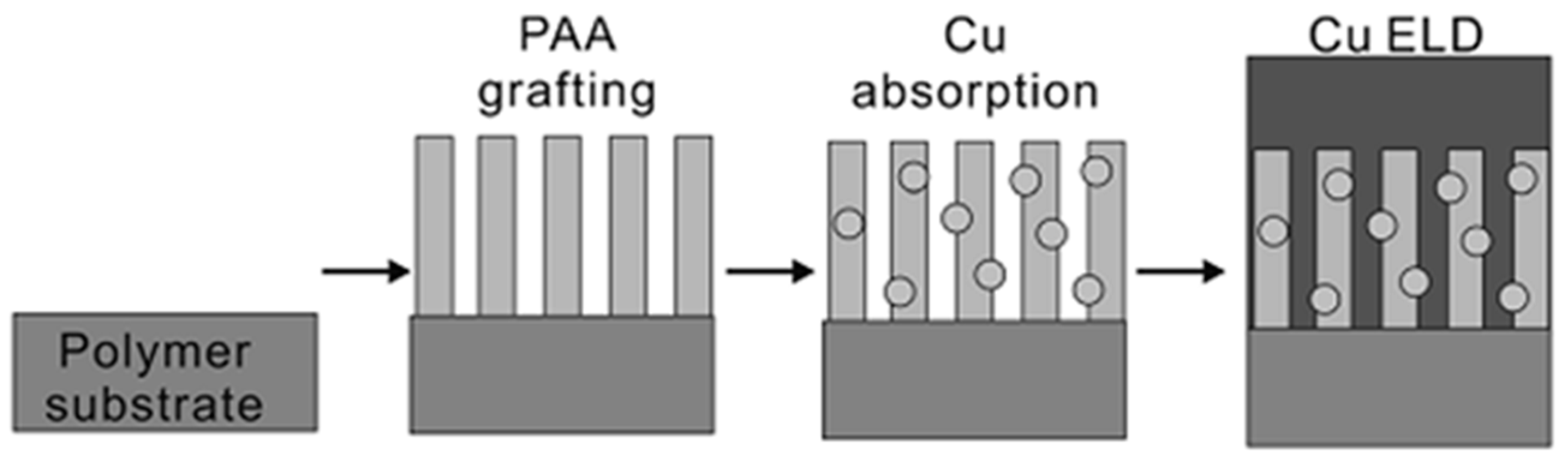
Figure 6.
An explanation of mixed-polymer-matrix catalytic ELD. Positively and negatively charged polymers build highly selective copper and nickel layers [47].
Figure 6.
An explanation of mixed-polymer-matrix catalytic ELD. Positively and negatively charged polymers build highly selective copper and nickel layers [47].

Figure 7.
The process of ELD of a folded golden film via the treatment of post-modification of a surface-grafted PAA layer on a PDMS substrate [52].
Figure 7.
The process of ELD of a folded golden film via the treatment of post-modification of a surface-grafted PAA layer on a PDMS substrate [52].

Figure 8.
Schematic illustration of the production of PMIA-PDA-Ag fibres by PDA-assisted electroless silver deposition [53].
Figure 8.
Schematic illustration of the production of PMIA-PDA-Ag fibres by PDA-assisted electroless silver deposition [53].

Figure 9.
The process of the fabrication of Catkins-Ag microtubes by TA-assisted ELD [34].
Figure 9.
The process of the fabrication of Catkins-Ag microtubes by TA-assisted ELD [34].
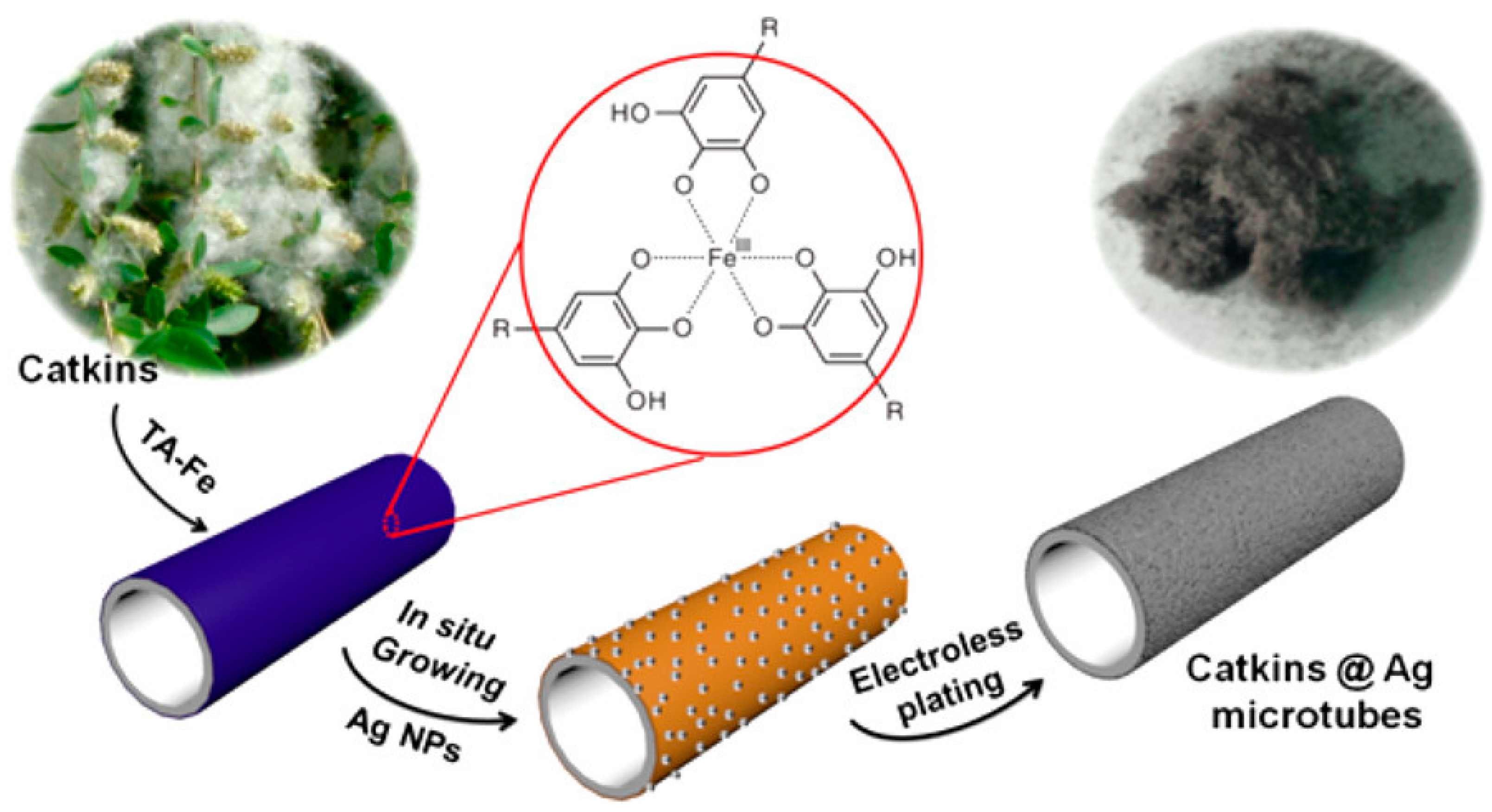
Figure 10.
(A)/(B) are photographs of the PET sheet with the copper film; (C) is an optical image of the part in (B); (D)/(E) are Scanning Electron Microscopy (SEM) pictures of the copper structures on substrates of PET (D) and PVDF (E) [45].
Figure 10.
(A)/(B) are photographs of the PET sheet with the copper film; (C) is an optical image of the part in (B); (D)/(E) are Scanning Electron Microscopy (SEM) pictures of the copper structures on substrates of PET (D) and PVDF (E) [45].

Figure 11.
(A) An illustration of the synthesis process of a stretchable conductor on an elastomer substrate; (B) the optical microscopy images of copper layers of ELD on rubber at different tensile strains (from 0% to 70%) [37].
Figure 11.
(A) An illustration of the synthesis process of a stretchable conductor on an elastomer substrate; (B) the optical microscopy images of copper layers of ELD on rubber at different tensile strains (from 0% to 70%) [37].
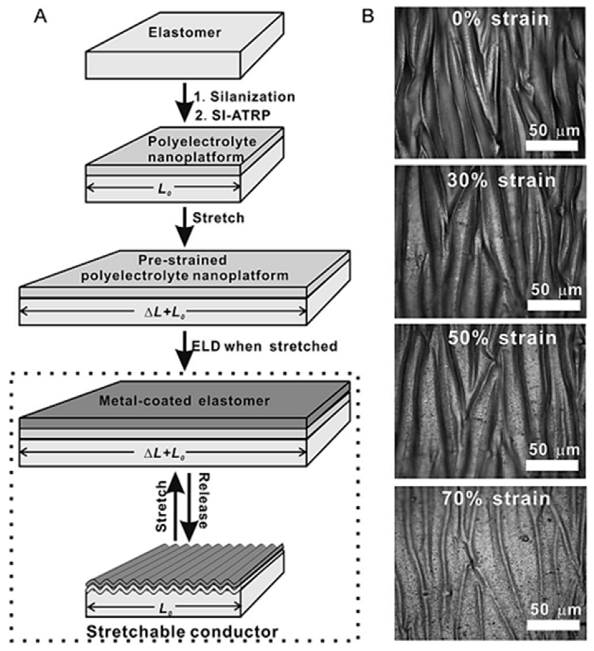
Figure 12.
(A) The changes in conductivity of the high stretchable conductor at different tensile strains; (B) the changes of durability in conductivity at various stretching cycles when the tensile strains are 0% and 70%, respectively; (C)/(D) digital images of the high stretchable conductor linked with a light-emitting diode at 0% (C) and 70% (D) tensile strains; (E)/(F) digital images of the copper film with rubber substrate at 0% (E) and 300% (F) tensile strains [9,37].
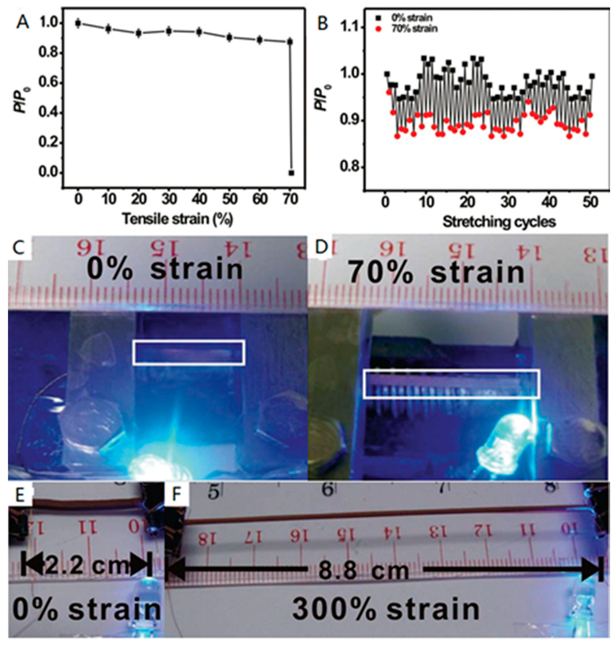
Figure 13.
The processes of fabricating the metal particles on the cotton substrate through ELD [54].
Figure 13.
The processes of fabricating the metal particles on the cotton substrate through ELD [54].
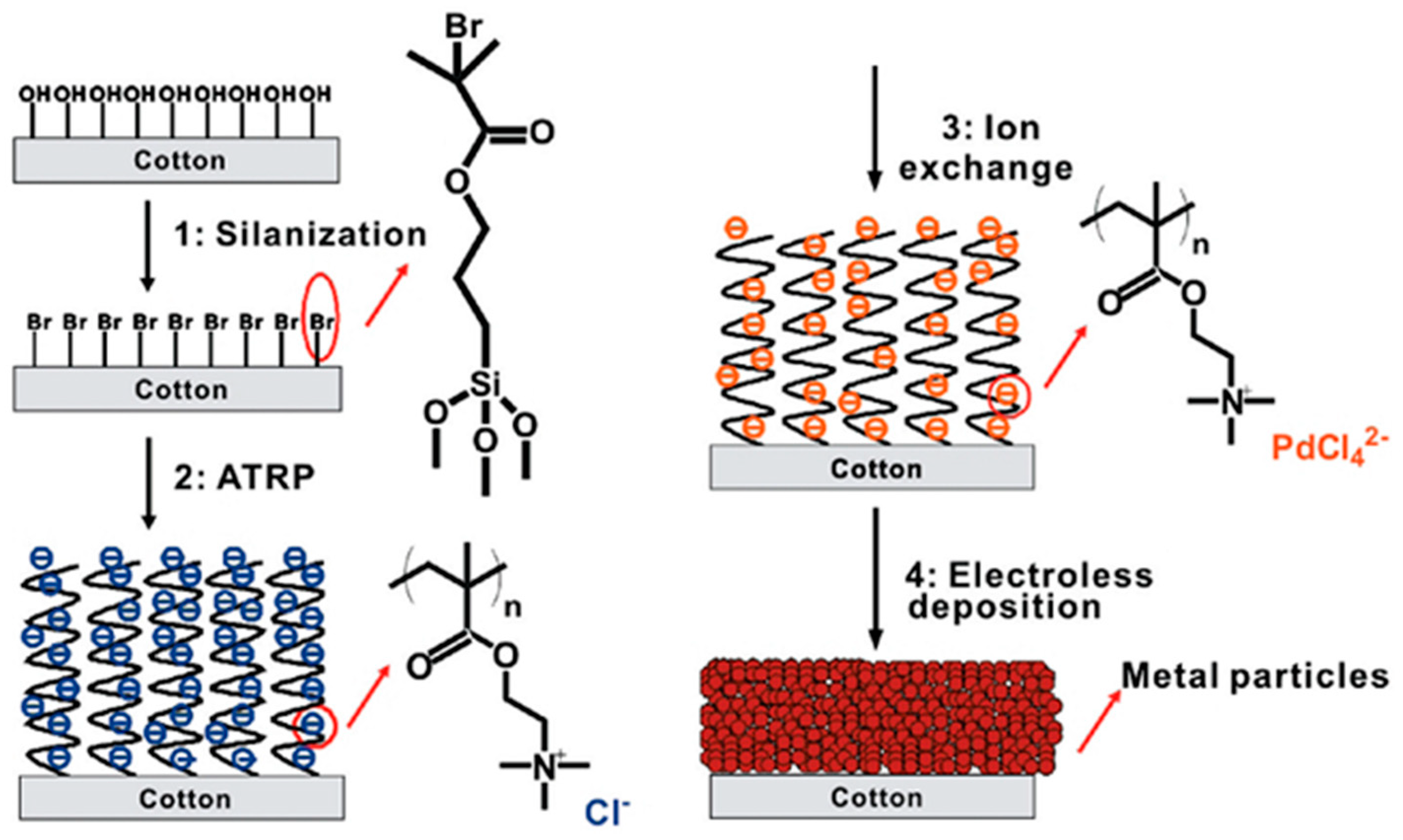
Figure 14.
Digital images show an electrical wire (A) and conductive yarn (B) that are both linked with an LED [54].
Figure 14.
Digital images show an electrical wire (A) and conductive yarn (B) that are both linked with an LED [54].
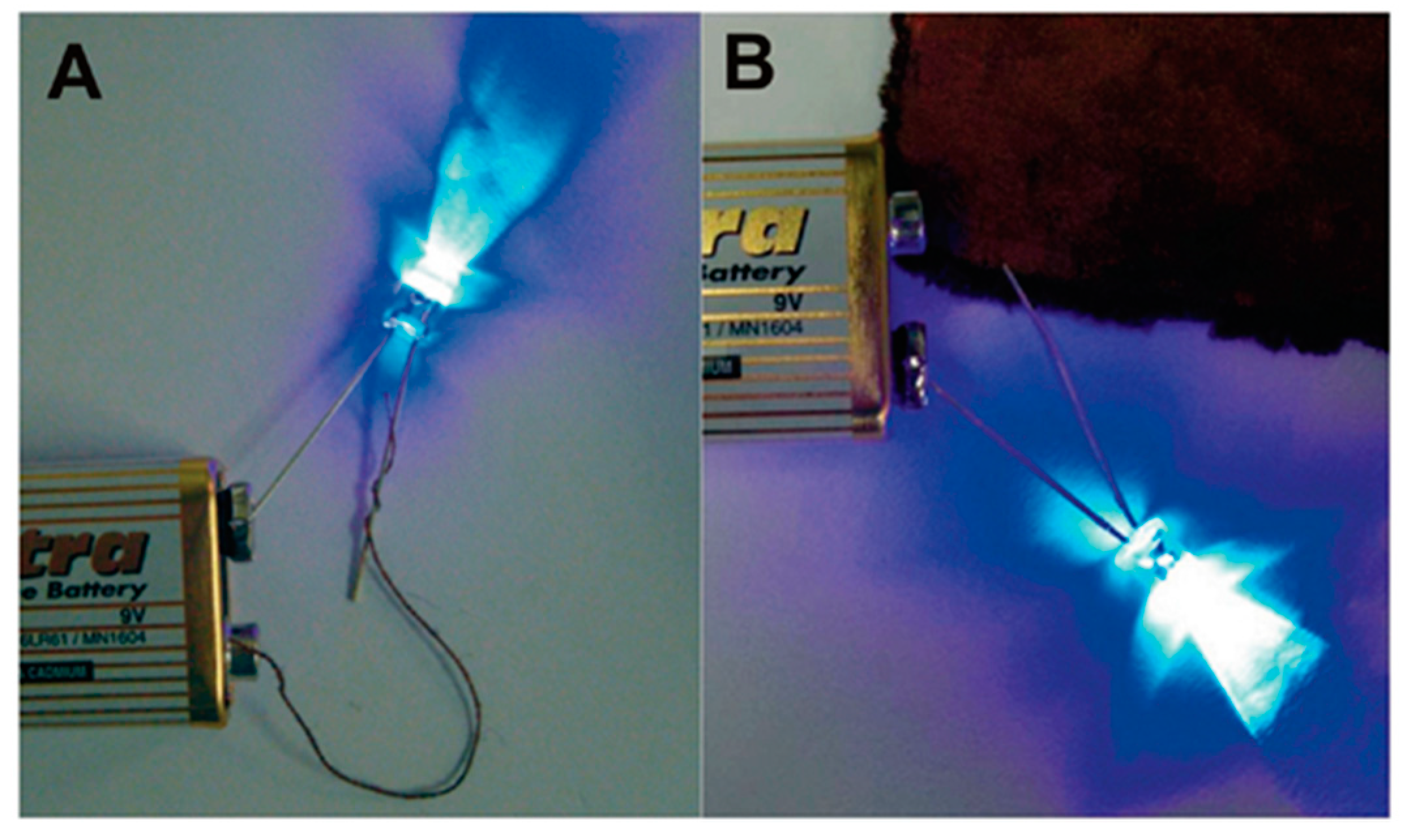
Figure 15.
The process of ELD to produce vein-based transparent electrodes [10].
Figure 15.
The process of ELD to produce vein-based transparent electrodes [10].

Figure 16.
Random test about bulk resistances in different parts of the vein conductor [10].
Figure 16.
Random test about bulk resistances in different parts of the vein conductor [10].

Figure 17.
Glue was used to attach LEDs to the modified seam; it worked well when the wire stayed in various shapes: (A) flat vein-based transparent electrodes (B) bended vein conductors [10].
Figure 17.
Glue was used to attach LEDs to the modified seam; it worked well when the wire stayed in various shapes: (A) flat vein-based transparent electrodes (B) bended vein conductors [10].

Figure 18.
Processes of creating a three-dimensional metal conductor through polymer-matrix catalytic ELD [39].
Figure 18.
Processes of creating a three-dimensional metal conductor through polymer-matrix catalytic ELD [39].

Figure 19.
Digital images of conductive three-dimensional sponges with working LEDs on the surface at various strains and shapes: (A) twisted (B) bended (C) stretched at 30% strain (D) compressed at 30% strain [39].
Figure 19.
Digital images of conductive three-dimensional sponges with working LEDs on the surface at various strains and shapes: (A) twisted (B) bended (C) stretched at 30% strain (D) compressed at 30% strain [39].

Figure 20.
Illustration of the conductive three-dimensional sponges before (A) and after (B) cutting some parts away [39].
Figure 20.
Illustration of the conductive three-dimensional sponges before (A) and after (B) cutting some parts away [39].
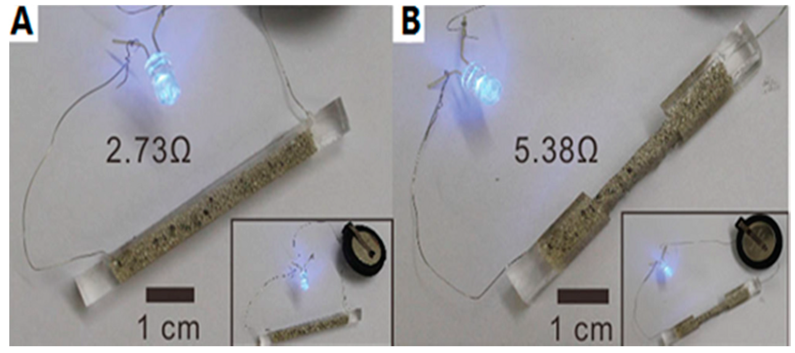
Figure 21.
An illustration of ELD of metal films through dip-pen nanolithography, inkjet printing and screen printing [27].
Figure 21.
An illustration of ELD of metal films through dip-pen nanolithography, inkjet printing and screen printing [27].

Table 1.
Current results of PIME catalytic ELD.
| Polymer Matrices | Polymerisation Method | Metal | Substrate |
|---|---|---|---|
| PMETAC [35,36,37,47] | SI-ATRP | Cu, Ni | Cotton, PET, PDMS, Au |
| PAA [40,42,44,45] | GraftFast, block copolymer | Cu, Ni | ABS, PET, PVDF, PAN, PB, PS |
| PVBVN [55] | Plasma grafting | Ag | PI |
| PMEP [47] | SI-ATRP | Cu, Ni | Au |
| PAA post-modified with ethylenediamine [52] | UV grafting | Au | PDMS |
| P2VP, P4VP [56,57,58,59,60,61,62,63,64] | UV, plasma, radiation grafting | Cu, Ni | PI, FPI, PTFE, silk, PVDF |
| PAM [56,65] | Radiation grafting | Cu | PP |
| PVP [65] | Radiation grafting | Cu | PE |
| PAN [51] | UV grafting | Cu | FEP |
| PHEA, PHMMAAm [50] | UV grafting | Cu | PTFE |
| PDDA [48,49] | Oxidative grafting | Cu | PTFE, glass |
| Dopamine [53] | Self-polymerisation | Ag | PIMA |
| Tannic Acid [34] | dip-coating | Ag | Catkin |
PDDA = Poly(diallyldimethylammonium chloride), PVBVN = Poly-(1,1′-bis(4-vinylbenzyl)-4,4′-bipyridinium dinitrate), PHEA = Poly-2-hydroxyethyl acrylate, PHMMAAm = Poly-N-(hydroxymethyl) methacrylamide.
© 2018 by the authors. Licensee MDPI, Basel, Switzerland. This article is an open access article distributed under the terms and conditions of the Creative Commons Attribution (CC BY) license (http://creativecommons.org/licenses/by/4.0/).
Share and Cite
MDPI and ACS Style
Zhu, C.; Li, Y.; Liu, X. Polymer Interface Molecular Engineering for E-Textiles. Polymers 2018, 10, 573. https://doi.org/10.3390/polym10060573
AMA Style
Zhu C, Li Y, Liu X. Polymer Interface Molecular Engineering for E-Textiles. Polymers. 2018; 10(6):573. https://doi.org/10.3390/polym10060573
Chicago/Turabian StyleZhu, Chuang, Yi Li, and Xuqing Liu. 2018. "Polymer Interface Molecular Engineering for E-Textiles" Polymers 10, no. 6: 573. https://doi.org/10.3390/polym10060573
Note that from the first issue of 2016, this journal uses article numbers instead of page numbers. See further details here.