A Screen Method for the Mass-Production of the Small-Size and Side-View LED Package

1
Department of Electronic Engineering, National Formosa University, Yunlin 632, Taiwan
2
Department of Electro-Optical Engineering & Graduate Institute of Electro-Optical and Materials Science, National Formosa University, Yunlin 632, Taiwan
*
Author to whom correspondence should be addressed.
Crystals 2018, 8(9), 350; https://doi.org/10.3390/cryst8090350
Submission received: 14 July 2018
/
Revised: 9 August 2018
/
Accepted: 28 August 2018
/
Published: 31 August 2018
(This article belongs to the Special Issue Selected Papers from Taiwan Association for Academic Innovation, TAAI 2018)
Abstract
:In this study, the small-size and side-view LED packages used in the backlight modules were examined by performing the electrostatic discharge (ESD) process. The high voltages used for the ESD process were 2 kV, 3 kV, and 4 kV. After ESD, the current–voltage curves were scanned from −7 V to 3 V. It was found that the significant leakage currents were in the reverse bias of 4 V~7 V and also in the forward bias of 1 V~2.5 V for ESD-damaged LED chips. However, the phenomenon of a slight increase in current was not found for the non-damaged samples. In our study case, the screening conditions could be set at a bias of −7 V or 2.3 V and the current of 0.1 µA.
1. Introduction
With the advance progress of display, the LED light bar plays an important role in every stage of progress. The lead frames used in light bars are generally side-viewed and with limited space for the circuit layout. Therefore, to put in a zener diode to protect the LED chip was, in general, not possible in most case. So, the strong anti-electrostatic ability was expected for those LED chips used in light bar products.
Review of the literature. Some efforts have been made to improve the anti-electrostatic ability of LED dies. Huang et al. [1] proposed an AlGaN/SiN buffer layer used underneath the UV LED. The live percent was improved from 68% to 86% following a 3 kV electrostatic discharge (ESD) test. Lee et al. [2] proposed a Si-doped graded superlattice layer embedded between the n-GaN layer and multi-quantum-wells (MQWs). This proved to be a good method to improve ESD characteristics. Except for those above who used epitaxy to improve ESD, many researchers employed the modified device process. For example, Chang et al. [3] proposed a post annealed ZnO film, and Li et al. [4] proposed an internal capacitor to enhance the ESD properties. Although these achievements could improve the yield of LED production, the yield, after all, could not reach 100% due to the limited purity of the precursor and the cleanness of the grown chamber. Therefore, how to screen out the weak LED die is of significant importance. Dal Lago et al. [5] measured the dynamic electroluminescence and current waveforms, and Jeong et al. [6] did an accelerated life test and suggested a screening policy to screen the leakage LED.
For mass production, we need a rapid method to screen out the leakage LED. The authors in Reference [6] suggested a screening criterion on the sub turn-on voltage, using the related larger leakage current which happened at the minor turn-on region and can be submitted to the auto tester. However, for those LED chips with weak anti-electrostatic ability, it is difficult to find some differences on the current–voltage curves, i.e., the LED dies with apparent I-V curve agree well with the ideal diode curve such that we cannot screen them out. To have a strong anti-electrostatic ability used in later applications, it is important to know how to screen out LED chips that have recessive weak constitutions but have a normal current–voltage curve.
In this study, the extra ESD tests were performed on the package LED lead frames. Especially, for lead frames, such as 3806 or 4014, which do not have enough space to parallel a zener diode [7]. The ESD voltages were set at 2 kV~4 kV throughout this study. After the ESD process, the current–voltage curves were measured by using Keithley 2400 source meter. Except for those fully passed or fully failed LED dies, an extra criterion of current–voltage curves was proposed and submitted to the auto testers as a confirmed result.
2. Experiments
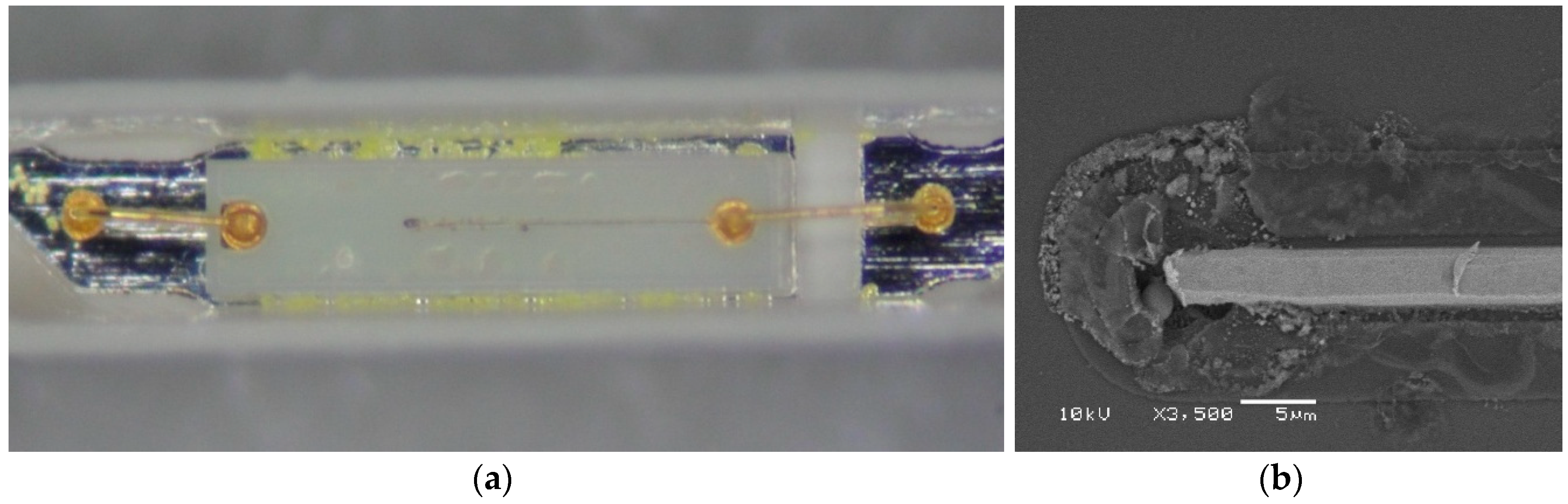
The ESD was carried out at a negative bias of 2 kV. At this moment, the LED dies were on top of the blue tape. Then, the small-size and side-view LED were die-bound and wire-bound onto the 4014 or 3806 lead frame products as shown in Figure 1a. These products were used as a light bar in the backlight modules, and did not have enough space to put a zener diode within it. Hence, these products were expected to have a higher anti-electrostatic ability. Therefore, it is important through the ESD process to stress and filter out those LED chips with poor electric characteristics.
A series of experiments were carried out by adopting the ESD voltage of 2 kV, 3 kV, and 4 kV on the LED chips. Then the current–voltage curves were measured by using the Keithley 2400 source meter (Keithley, Solon, OH, USA) at a different bias range. The scanning sample data points were set at about 501 points. The final test condition was performed on the commercial auto test machine.
3. Results and Discussion
Here, it is worth pointing out that our purpose for using ESD process is to discover the LED chips with weak junctions and to filter them out before they are used as a light bar product. In other words, we did not try to improve or remedy those LEDs with a weak constitution that may come from poor epitaxy or other device processes. These poor-quality LED chips need to be filtered out before being used in the light bar assembly production line. Figure 2 shows the current–voltage curves of the samples performed with an ESD voltage of 3 kV. From this figure, it was found that all samples have the similar curvature through the measuring bias range from −7 V to 3 V. At the reverse bias region, the signals of current levels were located under the background current signal which is the lowest level of the source meter at that environment. Therefore, we can conclude that these samples do not have a fault on the p-n junctions of the LEDs.
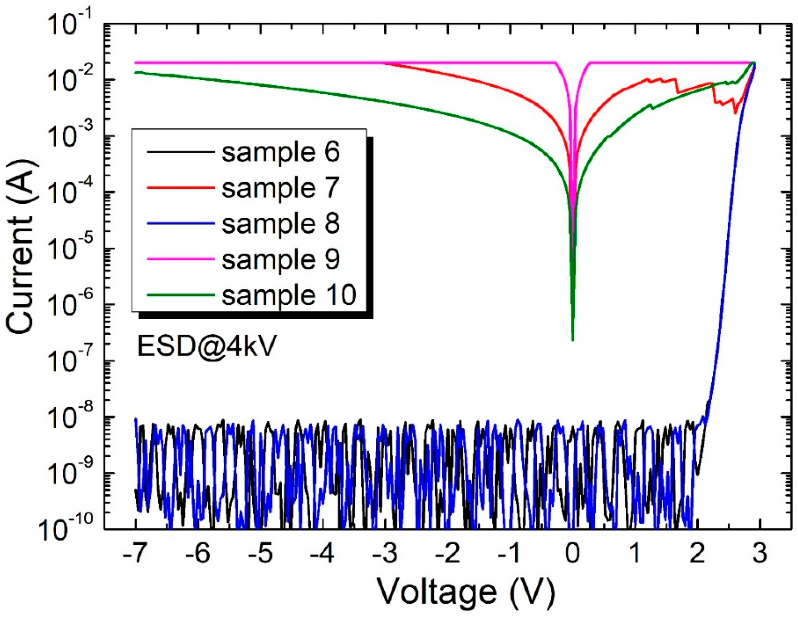
The current–voltage curves when the ESD process was increased to 4 kV are shown in Figure 3. It was found that about 60% of LED chips short-circuited. However, the results were divided into two extreme cases. One case passed and did not have any faults on the current–voltage curves. The other failed and are represented as a short in the p-n junction case. In general, the higher probability is that it happened at the p-electrode terminal end as shown in Figure 1b. However, it is not so easy to find the middle case which is not so healthy on current–voltage curve, but where the illumination power and turn-on voltage are still normal. In our actual production case, the probability was estimated about at parts-per-million level. Although we may perform the full current–voltage scan with the bias range of −7 V to 3 V for all samples, it wastes too much time in mass production and seems to violate the time budget.
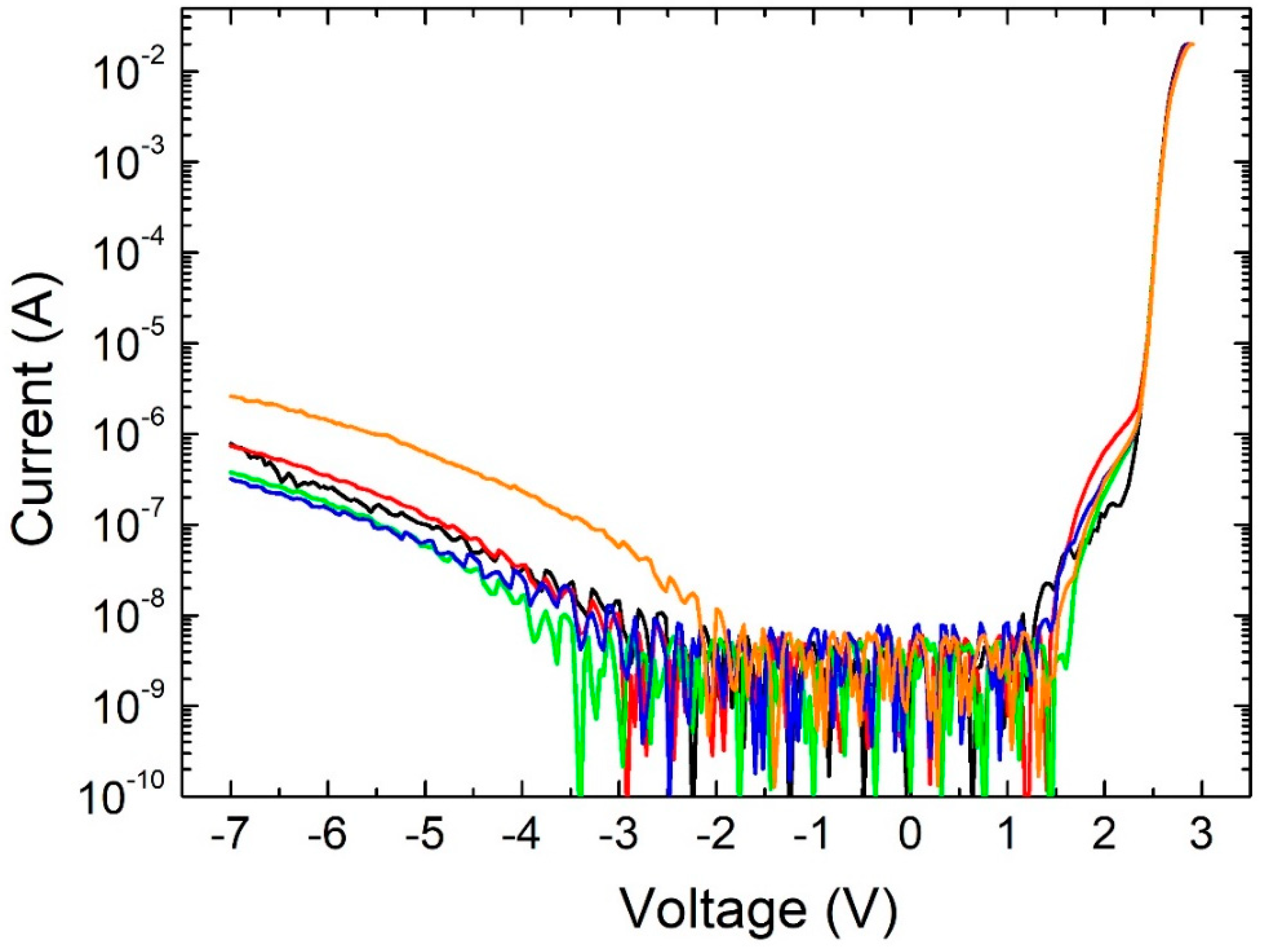
To have an excellent yield of LED packages used in backlights, the minor and poor chips found after the ESD was performed were studied and researched on their current–voltage curves. Figure 4 shows these curves with normal illumination power and turn-on voltage. More leakage currents were found in the reverse bias of 4 V~7 V for ESD-damaged LED chips. About 10 kk samples were done in this study. Compared to the pass/good LED chips, the current of the damaged chips need to, at least, have an order of contrast, and, thus, be easy to judge if they are damaged in the current–voltage curves. When we inspected the complete I-V curve, two significant leakage points were found. One is at the subthreshold region, and the other is at the breakdown region. Therefore, the auto test condition in the back end of package process was set at a reverse bias of 7 V and the corresponding reverse leakage current was set at a current of 0.1 µA. In another viewpoint, it can be concluded that the breakdown voltage was lowered after ESD treatment while the minor damage was formed. But for the passed samples, we did not observe this phenomenon. On the other hand, we also have a chance to detect and filter out the damaged LED chips when we focused on the forward bias of 1 V~2.5 V. They also have a significant increase in the forward current for the damaged chips. The criterion to identify the detective voltage is located at the subthreshold region where the current has a maximum contrast. In our experiments, the filter conditions could be set at a bias of 2.3 V and the current of 0.1 µA.
4. Conclusions
In summary, the significant leakage currents were found in the reverse bias of 4 V~7 V for ESD-damaged LED chips. Compared to the pass/good LED chips, the current of the damaged chips need to, at least, have an order of contrast in the subthreshold or breakdown region, and, thus, be easy to judge if they are damaged in the current–voltage curves. Therefore, the auto test condition in the back end of the package process was set at a reverse bias of 7 V, and the corresponding reverse leakage current was set at a current of 0.1 µA. On the other hand, we also have a chance to detect and screen out the damaged LED chips when we focused on the forward bias of 1 V~2.5 V. They also have a significant increase in the forward current for the damaged chips. The filter conditions could be set at a bias of 2.3 V and the current of 0.1 µA. The suitable ESD voltage for our case was 3 kV.
Author Contributions
Individual contributions for this research. Conceptualization, W.-R.C. and Y.-S.L.; Methodology, W.-R.C. and Y.-S.L.; Validation, W.-R.C.; Formal Analysis, W.-R.C.; Investigation, W.-R.C.; Data Curation, W.-R.C. and Y.-S.L.; Writing-Original Draft Preparation, W.-R.C.; Writing-Review & Editing, W.-R.C.; Visualization, W.-R.C.
Funding
This research was funded by Power Logic Company grant number 107-AF-045.
Acknowledgments
This work was partially supported by National Formosa University under the contract number of 107-AF-045.
Conflicts of Interest
The authors declare no conflict of interest.
References
- Huang, G.S.; Kuo, H.C.; Lo, M.H.; Lu, T.C.; Tsai, J.Y.; Wang, S.C. Improvement of efficiency and ESD characteristics of ultraviolet light-emitting diodes by inserting AlGaN and SiN buffer layers. J. Cryst. Growth 2007, 305, 55–58. [Google Scholar] [CrossRef]
- Lee, K.; Lee, C.R.; Chung, T.H.; Park, J.; Leem, J.Y.; Jeong, K.U.; Kim, J.S. Influences of graded superlattice on the electrostatic discharge characteristics of green InGaN/GaN light-emitting diodes. J. Cryst. Growth 2017, 464, 138–142. [Google Scholar] [CrossRef]
- Chang, L.B.; Chang, Y.S.; Jeng, M.J.; Liu, K.C.; Yang, J.F.; Kuo, S.Y.; Wu, K.H. High ESD reliability InGaN light emitting diodes with post deposition annealing treated ZnO films. Solid State Electron. 2012, 77, 77–81. [Google Scholar] [CrossRef]
- Li, P.; Li, H.; Zhao, Y.; Kang, J.; Li, Z.; Liu, Z.; Yi, X.; Li, J.; Wang, G. Excellent ESD Resistance Property of InGaN LEDs With Enhanced Internal Capacitance. IEEE Photon. Technol. Lett. 2015, 27, 2004–2006. [Google Scholar] [CrossRef]
- Dal Lago, M.; Meneghini, M.; De Santi, C.; Barbato, M.; Trivellin, N.; Meneghesso, G.; Zanoni, E. ESD on GaN-based LEDs: An analysis based on dynamic electroluminescence measurements and current waveforms. Microelectron. Reliab. 2014, 54, 2138–2141. [Google Scholar] [CrossRef]
- Jeong, J.S.; Jung, J.K.; Park, S.D. Reliability improvement of InGaN LED backlight module by accelerated life test (ALT) and screen policy of potential leakage LED. Microelectron. Reliab. 2008, 48, 1216–1220. [Google Scholar] [CrossRef]
- Sun, Y.X.; Chen, W.S.; Hung, S.C.; Lam, K.T.; Liu, C.H.; Chang, S.J. GaN-Based Power Flip-Chip LEDs With an Internal ESD Protection Diode on Cu Sub-Mount. IEEE Trans. Adv. Packag. 2010, 33, 433–437. [Google Scholar] [CrossRef]
Figure 1.
(a) Topography of the side view LED package, and (b) the image of burn out p-pad after the electrostatic discharge (ESD) process.
Figure 1.
(a) Topography of the side view LED package, and (b) the image of burn out p-pad after the electrostatic discharge (ESD) process.

Figure 2.
Current–voltage curves after an ESD bias of 3 kV. All samples were passed.
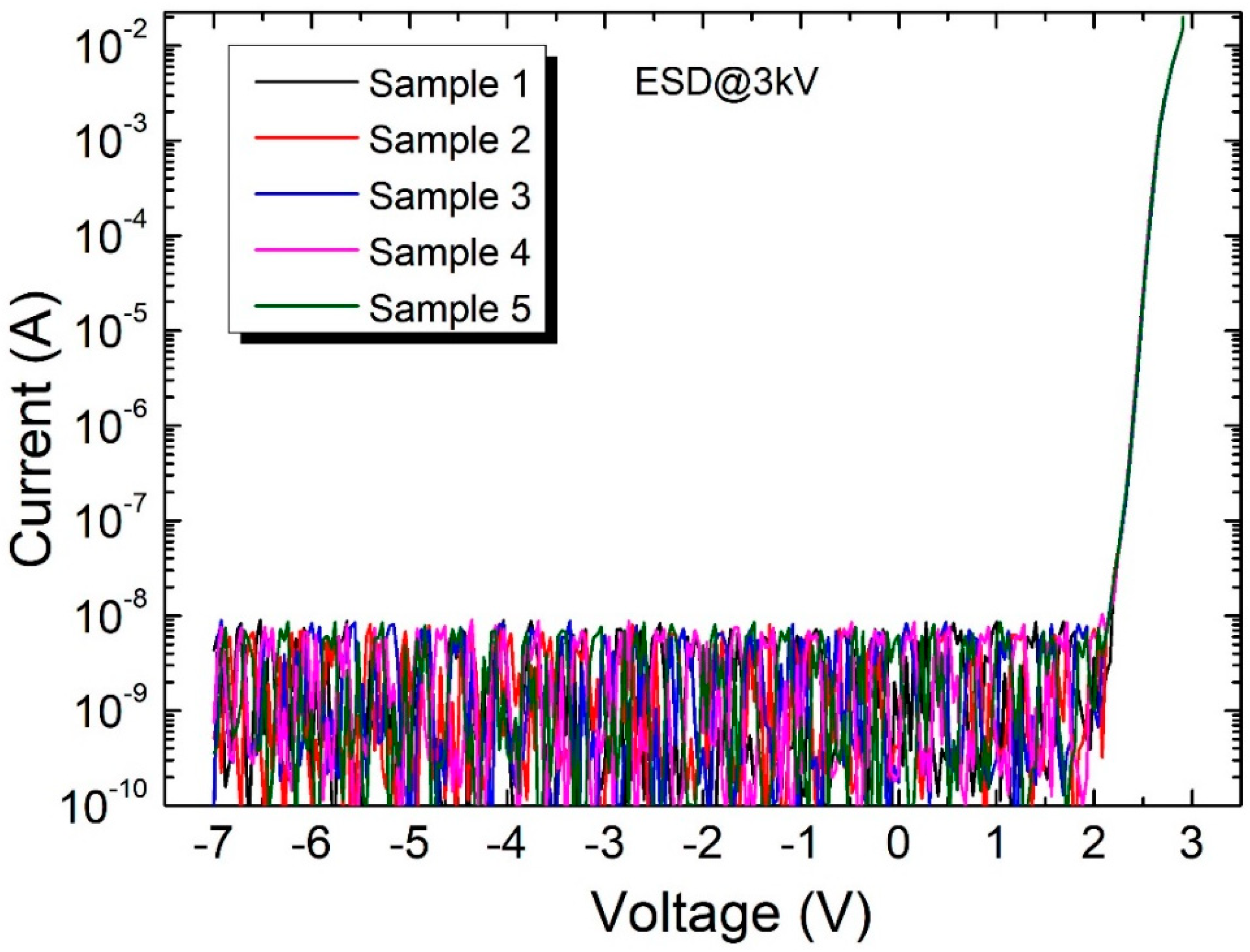
Figure 3.
Current–voltage curves after an ESD bias of 4 kV. Three samples were failed, and two samples were passed.
Figure 3.
Current–voltage curves after an ESD bias of 4 kV. Three samples were failed, and two samples were passed.

Figure 4.
Current-voltage curves of the damaged LED chips.
© 2018 by the authors. Licensee MDPI, Basel, Switzerland. This article is an open access article distributed under the terms and conditions of the Creative Commons Attribution (CC BY) license (http://creativecommons.org/licenses/by/4.0/).
Share and Cite
MDPI and ACS Style
Chen, W.-R.; Luo, Y.-S. A Screen Method for the Mass-Production of the Small-Size and Side-View LED Package. Crystals 2018, 8, 350. https://doi.org/10.3390/cryst8090350
AMA Style
Chen W-R, Luo Y-S. A Screen Method for the Mass-Production of the Small-Size and Side-View LED Package. Crystals. 2018; 8(9):350. https://doi.org/10.3390/cryst8090350
Chicago/Turabian StyleChen, Wen-Ray, and You-Sheng Luo. 2018. "A Screen Method for the Mass-Production of the Small-Size and Side-View LED Package" Crystals 8, no. 9: 350. https://doi.org/10.3390/cryst8090350
Note that from the first issue of 2016, this journal uses article numbers instead of page numbers. See further details here.