Metal Halide Perovskite Single Crystals: From Growth Process to Application
by
 and
and
Shuigen Li
1,*, 
Chen Zhang
2,
Jiao-Jiao Song
2,
Xiaohu Xie
1,
Jian-Qiao Meng
2,3,* and
Shunjian Xu
1,* 1
School of New Energy Science and Engineering, Xinyu University, Xinyu 338004, China
2
Hunan Key Laboratory for Super-Microstructure and Ultrafast Process, School of Physics and Electronics, Central South University, Changsha 410083, China
3
Synergetic Innovation Center for Quantum Effects and Applications (SICQEA), Hunan Normal University, Changsha 410081, China
*
Authors to whom correspondence should be addressed.
Crystals 2018, 8(5), 220; https://doi.org/10.3390/cryst8050220
Submission received: 21 April 2018
/
Revised: 9 May 2018
/
Accepted: 9 May 2018
/
Published: 17 May 2018
(This article belongs to the Special Issue Metal Halide Perovskite Crystals: Growth Techniques, Properties and Emerging Applications)
Abstract
:As a strong competitor in the field of optoelectronic applications, organic-inorganic metal hybrid perovskites have been paid much attention because of their superior characteristics, which include broad absorption from visible to near-infrared region, tunable optical and electronic properties, high charge mobility, long exciton diffusion length and carrier recombination lifetime, etc. It is noted that perovskite single crystals show remarkably low trap-state densities and long carrier diffusion lengths, which are even comparable with the best photovoltaic-quality silicon, and thus are expected to provide better optoelectronic performance. This paper reviews the recent development of crystal growth in single-, mixed-organic-cation and fully inorganic halide perovskite single crystals, in particular the solution approach. Furthermore, the application of metal hybrid perovskite single crystals and future perspectives are also highlighted.
1. Introduction
Recently, organic-inorganic metal hybrid perovskites have shown great applied potential because of their impressive optical and electrical properties [1,2,3,4,5], which can be represented by the structure ABX3, where A is CH3NH3+, CH(NH2)2+ or Cs+, B is Pb2+ or Sn2+, and X is I–, Br– or Cl– [6,7,8,9,10,11,12,13,14,15,16,17,18,19,20,21,22,23,24,25,26,27]. The ideal ABX3 structure is cubic symmetry, where A and B ions are located at the eight corners and center of a cubic unit, respectively. The symmetry of ABX3 structures is based on the atomic species of the A and B sites. In a typical perovskite crystal structure, the A, B, and X ionic radii, e.g., RA, RB, and RX, should correspond to a specific geometric relationship, known as the Tolerance factor [28,29,30]: t = (RA + RX)/(RB + RX). The ideal value of t should be 1 for cubic structures; otherwise, the structure tends to be distorted, or even destroyed [28,30,31]. For lead hybrid perovskite, the large organic cation at the A position, e.g., methylammonium (MA+) or formamidinium (FA+), is able to match the large radius of the Pb2+ ion at the B position and meet the tolerance factor t, while the halogen anions or their mixtures occupy the C positions, resulting in the formation of a 3D perovskite structure [32]. These perovskite-based materials, when used in the photovoltaic field, can provide remarkable properties, such as broad absorption from the visible to the near-infrared region, tunable optical and electronic properties [15,33,34,35,36], high charge mobility, and long exciton diffusion length and carrier recombination lifetime [32,37,38,39,40,41,42,43,44,45,46,47,48]. Within a few years, they have revolutionized the photovoltaic field; an efficiency of 22.1% from solution-processable perovskite-based solar cells has been reported [49]. In addition, lead hybrid perovskites have also been used in some other fields, such as laser [50], photodetector [51], light-emitting-diodes [52], thermoelectricity [53], and catalysis [54], demonstrating their potential application prospects.
Until now, many intensive investigations have been based on polycrystalline thin films, one of the existing forms of perovskite, and most of the results have been focused on the perovskite polycrystalline film. With in-depth research, single crystals—another form of perovskite—have been found with low defect density. The carrier diffusion length of perovskite is sensitive to defects. When expanding the grain size, the carrier diffusion length of polycrystalline forms can increase to up to 1 μm, while large single crystals are able to provide even longer carrier diffusion lengths. Dong et al. prepared millimeter-sized MAPbI3 single crystals via a low-temperature solution approach, in which a carrier diffusion length of over 175 μm was obtained under 1 sun illumination, and a longer carrier diffusion length exceeding 3 mm could be produced under a weaker illumination with 0.003% sun illumination [55]. Shi et al. reported low trap-state density of states with an order of 109–1010 cm−3 and carrier diffusion length > 10 mm in MAPbX3 single crystals [40]. The longer carrier diffusion length in single crystals with low trap-state density derives from their better extraction and transport of photogenerated charge carriers, resulting in a performance boost for optoelectronic devices. These meaningful findings will contribute to the development of perovskite-based materials, and will be extremely beneficial to further fundamentally investigate the intrinsic properties of perovskites single crystals. To date, single-organic-cation, mixed-organic-cation, and all-inorganic kinds of metal halide perovskite single crystals have been demonstrated. In this review, we will summarize the advances in the growth and application of the above perovskite single crystals.
2. Growth of Organic-Inorganic Hybrid Halide Perovskite Single Crystals
Since organic-inorganic metal hybrid perovskite solar cells (PSCs) were studied for the first time [5], they have attracted particular attention due to their extraordinary performance. Since then, in-depth study on perovskite-based materials and devices has been carried out, and a series of research results have been obtained. Meanwhile, perovskite single crystals, which were reported about forty years ago [40,56,57], are studied again.
2.1. Growth of Single-Organic-Cation Halide Perovskite Single Crystals
Solution temperature lowering (STL) is a traditional single crystal growth process. In 1987, Poglitsch et al. gained MA-based perovskite single crystals via a temperature-lowering method [58] in which they heated the mixed solution to 100 °C, and perovskite single crystals were grown by cooling the solution to room temperature. In general, minimizing the number of nuclei is crucial to growing large single crystals. As an improved technology, seed-assisted growth is often adopted for the purpose of growing large-sized and high-quality single crystals, i.e., small crystals are firstly put into a single crystal precursor, followed the temperature-lowering process. Using a slow cooling rate of 0.1–0.2 °C/h, Su et al. obtained large MAPbI3 single crystals with sizes of up to 1 cm [59] by a process in which small crystals were firstly obtained by spontaneous nucleation (Figure 1a), then high-quality as-grown crystals were selected as seeds and dropped back into the mother liquid to grow large single crystals (Figure 1b). Similarly, MAPbBr3 single crystals with perfect cubic structure were formed. Dang et al. grew tetragonal MAPbI3 bulk single crystals with dimensions of 10 mm × 10 mm × 8 mm by a seed-assisted growth method [60] in which the seeded crystal was fixed in the middle of the solution. The solution was saturated gradually with a decrease of temperature from 65 °C to 40 °C, resulting in the formation of high-quality single crystals over the following few days.
Huang’s [36] group grew large bulk MAPbI3 single crystals with a size of 10 mm × 3.3 mm via a temperature-lowering method, as presented in Figure 1c, in which the seed crystal was fixed in the top half of the solution. Importantly, they dissolved the seed crystals in the bottom of the precursor solution, and the super saturation of the top solution was readily induced because of the temperature gradient between the top and bottom, leading to fast-growing of single crystals with a rate of about 2 mm per day.
Using the bottom-seeded solution growth (BSSG) method, Lian et al. [61] prepared centimeter-sized bulk MAPbI3 single crystals. To eliminate the negative effect of multiple nuclei, a seed crystal was fixed by platinum wire to segregate the seed crystal from the bottom of the flask, and the desired single crystal, 12 mm × 12 mm × 7 mm in size, was obtained by lowering the temperature of the growth solution from 373 K to 330 K, as shown in Figure 1d.
Tin-based perovskite single crystals have also been harvested by the temperature-lowering method. Tao and co-worker reported bulk cubic CH3NH3SnI3 and CH(NH2)2SnI3 single crystals grown via a top-seeded solution growth (TSSG) method (Figure 1e,f) [62]. Similarly, NH(CH3)3SnX3 (X = Cl, Br) single crystals were prepared via the TSSG method [63], as shown in Figure 1g,h.
Lian et al. reported a rapid solution temperature-lowering method to prepare Mixed-halide perovskite single crystals based on the addition of chlorine [64]. With the addition of chlorine, the surface free energy and the edge free energy were changed. The resulting edge free energy is expressed by: ρChlorine = ρ − kBT ln CChlorine, given that the edge free energy ρChlorine decreases with CChlorine, the growth rate of CH3NH3PbI3(Cl) crystal face will increase. They harvested large CH3NH3PbI3(Cl) with sizes of 20 mm × 18 mm × 6 mm within only 5 days (Figure 1i) that possessed excellent properties, i.e., a high carrier mobility of 167 ± 35 cm2·V−1·s−1, a low trap-state density of 7.6 × 108 cm−3, and a transient carrier lifetime as long as 449 ± 76 μs. Mixed-halide perovskite single crystals can also be grown via solw temperature-lowering method [65]. At 100 °C, a super-saturated aqueous solution, including single or mixed haloid acid of different halide ratios, mixing methylamine and lead (II) acetate, was prepared. By gradually lowering the precursor solution temperature, a series of perovskite single crystals, depending on the different halide ratios, could readily be formed, as presented in Figure 1j. As is shown, for both MAPbBr3−xClx and MAPbI3−xBrx single crystals, the color varies with the different halide ratios of Br/(Cl + Br) and I/(I + Br).
The STL method provides a simple and effective approach for the growth of MAPbX3 and FAPbX3, in which the crystals are formed with the decrease in the temperature of the precursor solution. However, the drawback of its being highly time-consuming (typically more than two weeks to gain one-centimeter-sized crystals [61,62]) limits its extensive use. On the other hand, the solute solubility in solvents decreases with increasing temperature for a few materials [66], i.e., inverse temperature solubility, which is also present for organic-inorganic metal hybrid perovskites. For example, MAPbI3, MAPbBr3 and MAPbCl3 show inverse temperature solubility in certain solvents-gamma-butyrolactone (GBL), N,N-dimethylformamide (DMF), and dimethylsulfoxide (DMSO), respectively. Based on the above characteristics, inverse temperature crystallization (ITC) was first introduced to grow MAPbI3 single crystals. During the ITC, the precursor was dissolved in GBL and the temperature was increased until single crystals formed at about 190 °C [67]. At the same time, Saidaminov et al. designed inverse temperature crystallization (ITC) for MAPbX3 perovskites due to their inverse temperature solubility behavior in some solvents [68]. They grew size- and shape-controlled high-quality MAPbI3 and MAPbBr3 single crystals within several hours (Figure 2a).
To grow large single crystals and understand their growth mechanism, Liu’s group developed the seed-repeated method and harvested the largest MAPbI3 single crystal, with a size of 71 mm × 54 mm × 39 mm, as well as inch-sized MAPbBr3 and MAPbCl3 crystals (Figure 2g) [69]. In the process of crystal growth, small perovskite particulates were harvested as seed crystals to keep in precursor solution at 100 °C for 24 h. A seed crystal was placed in precursor solution to keep at 100 °C for 48 h, resulting in the formation of a larger crystal. By repeating the above process, the final large crystals would be produced. Figure 2j shows the absorbance spectra of MAPbX3 (X = Cl, Br, I) perovskites. A clear band edge without excitonic signature or absorption is shown, indicating high-quality single crystals with low defect concentration. Furthermore, all of the PL spectra of MAPbCl3, MAPbBr3, and MAPbI3 perovskites exhibited narrow PL peaks at ≈402, ≈537, and ≈784 nm, respectively (Figure 2k), and the PL peak values were smaller than the corresponding absorption onsets (431, 574, and 836 nm), indicating their advantageous application in solar cells. The X-ray Diffraction (XRD) measurement displayed that the (200) diffraction peak of MAPbI3 single crystal showed a FWHM of 0.3718°, which indicated that the single crystal held a respectable crystalline quality. Electric characterization showed that the electron trap was 1.1 × 1011 cm−3 for MAPbBr3 and 4.8 × 1010 cm−3 for MAPbI3. The hole trap densities for MAPbBr3 and MAPbI3 were determined to be 2.6 × 1010 cm−3 and 1.8 × 109 cm−3, respectively. Furthermore, the crystalline MAPbX3 (X = I, Cl, Br) gave a high carrier mobility of 34 cm2·V−1·s−1, 179 cm2·V−1·s−1 and 4.36 cm2·V−1·s−1. It is expected that such wafer-sized single-crystalline MAPbX3 (X = I, Cl, Br) with superior properties in terms of defect state and carrier density are promising materials for high-performance optoelectronic devices.
The ITC method is a highly effective approach for growing metal hybrid halide perovskite crystals that possesses a much faster growth rate than that of the typical STL method and has been used extensively to grow single or mixed halide perovskite crystalline materials [67,70,71,72,73,74]. Additionally, the ITC method meets the requirements of FAPbX3 single crystals. Bakr’s group reported the retrograde solubility of FA-based perovskites and grew high-quality crack-free FAPbI3 and FAPbBr3 single crystals (Figure 2h,i) [75]. By improving the onset of crystallization temperature, they obtained grain boundary-free FAPbI3 crystals within 3 h. Yang’s group obtained 5-mm-sized FAPbI3 single crystals for the first time via a modified ITC method [74]. They first grew the FAPbI3 seed crystal via a cooling solution method, followed by growing larger single crystals by placing the small seed crystals into the ITC precursor and keeping at 100 °C.
In addition to the above growth method based upon temperature, the antisolvent vapor-assisted crystallization (AVC) method, a temperature-independent process, was also developed [40]. In AVC, a proper anti-solvent slowly diffuses into the crystal precursor solution, resulting in formation of sizable MAPbX3. Using the AVC method, Bakr’s group [40] gained high-quality MAPbI3 and MAPbBr3 single crystals, and implemented a solvent with high solubility for MAX and PbX2, i.e., N,N-Dimethylformamide (DMF) or γ-butyrolactone (GBA). Dichloromethane (DCM) acted as the antisolvent to avoid the formation of hydrogen bonds due to its poor solubility for both PbX2 and MAX, thus minimizing asymmetric interactions with the ions during their assembly into crystal form. This approach created the conditions for the coprecipitation of the ionic building blocks of perovskite. When DCM diffused into DMF or GBA at a slow and controlled rate (Figure 3a), millimeter-sized MAPbBr3 and MAPbI3 single crystals were grown. As shown in Figure 3a, to obtain MAPbBr3 single crystals, PbBr2/MABr molar ratio of 1:1 was chosen and dissolved in DMF to form the precursor with PbI2 of 0.2 mol·L−1. For MAPbI3 single crystals, a precursor with PbI2/MAI molar ratio of 1:3 was dissolved in GBA, and PbI2 of 0.5 mol·L−1 was prepared. In this case, high-quality MAPbX3 single crystals were obtained, with super-excellent performance. The absorbance of MAPbX3 (X = Br− and I−) (Figure 3e) exhibited a clear band edge cutoff without excitonic signature that showed a minimal number of in-gap defect states. This confirmed a carrier (holes) concentration of 5 × 10⁹–5 × 1010 cm−3. The time-dependent PL signals of MAPbI3 and MAPbBr3 single crystals were obtained in order to quantify the carrier dynamics (Figure 3f), and showed a superposition of surface components (fast) τ ≈ 41 ns and bulk components (slow) τ ≈ 357 ns for MAPbBr3, and fast τ ≈ 22 ns and slow τ ≈ 1032 ns for MAPbI3. For MAPbBr3 single crystals, the carrier lifetime τ was also estimated by transient absorption (TA). It was shown that the fast component amounts to only 3.6% of the total TA signal in MAPbBr3, and to 7% and 12% of the total PL signal in MAPbI3 and MAPbBr3, respectively. As an alternative antisolvent, toluene can also effectively induce formation of MAPbBr3 single crystals (Figure 3b) with low surface recombination velocity (~(3.4 ± 0.1) × 103 cm·s−1) [76] through a process in which the crystal precursor is derived from dissolution of PbBr2 and MABr (1/1 by molar, 0.1 mol·L−1) in DMF. In another study, diethyl ether was reported as the antisolvent [77], in which HI served as the good solvent instead of organic solvents. Where PbI2 was firstly dissolved in HI solution upon heating to 120 °C, and formed a hot bright yellow solution; to the hot solution was added MAI, which dissolved immediately, leading to the formation of the crystal precursor. X-ray Diffraction (XRD) analysis revealed that an intermediate product of HxPbI2+x·xH2O was created because of the coordination between HI and PbI2. With inflow of diethyl ether into the precursor, MAPbI3 single crystals emerged developmentally. It’s worth mentioning that the growth mechanism of halide perovskite single crystals was studied. Recently, Chen et al. reported the growth mechanism of MAPbBr3 single crystal, which was synthesized by the antisolvent method [78]. The assembly model is shown in Figure 3c. CH3NH3Br·PbBr2·DMF adduct complex was first formed in the precursor solution, and crystallization occurred when the solution was supersaturated. The MAPbBr3 molecule in the saturated solution condensed into numerous small nuclei with the coalescence of the nuclei into bigger particles. The perovskite particles were gradually self-assembled into a hollow structure. The crystals were twisted, and their faces were peculiarly inclined toward each other. Subsequently, MAPbBr3 crystals exhibited a layered stacked structure, and continued to grow until the final single crystal was formed. Li and co-workers investigated the crystallization of MAPbI3−xBrx by adjusting the molar ratio of I/Br in precursor solution [79]. It was found that the crystallization and perovskite morphology were heavily affected by the composition of precursor solutions (Figure 3d). It was reported that Br has a smaller ionic radius and lower solubility in organic solvents because of the stronger bond strength [80]. As a comparison with PbBr2, PbI2 has a stronger electron-accepting ability and Lewis acidity [81]. Therefore, it was more likely to form needle crystals of MAPbI3−xBrx·DMF with high iodine concentration, which might lead to morphology evolution as the molar ratio of I/Br.
Bulk perovskite single crystals can show advanced properties, such as higher carrier mobility, longer carrier lifetime and diffusion length. However, bulk single crystals may cause degradation of device performance, because a thick active layer will increase the charge recombination. In this case, it is desirable to achieve the fabrication of perovskite single-crystal thin films, and thus to enhance the performance of the device. Bakr’s group grew MAPbBr3 monocrystalline film successfully via a cavitation-triggered asymmetrical (CTAC) strategy [82] in which a very short ultrasonic pulse was introduced to a low supersaturation level solution with antisolvent vapor diffusion; perovskite monocrystalline films were able to grow within several hours under the ultrasonic pulse. These obtained films were free of grain boundaries and were homogeneous, with the films having thicknesses ranging from one up to several tens of micrometers, and lateral dimensions varying from hundreds of microns to three millimeters, as shown in Figure 4a.
To obtain MAPbI3 perovskite single-crystalline wafer, Liu’s group designed an ultrathin geometry-defined dynamic-flow reaction system (Figure 4c) to obtain single crystals with different thicknesses and shapes (Figure 4d–m) [83]. It was shown that the two glass slides of the reaction system were separated and aligned in parallel by two spacers, leading to the single-crystalline wafer thickness and shape being defined by the spacers and slit channel design. Using the thickness-controllable reaction system, wafer as thin as about 150 μm with high crystallinity and a low trap state density of 6 × 108 cm−3 was prepared.
Chen et al. reported the controllable fabrication of air-stable, sub-millimeter-size perovskite single-crystalline thin films (SCTFs) [84]. For the preparation process, two flat substrates were clipped together and vertically immersed in perovskite precursor (Figure 5a), the thickness of the solution film could be easily tuned using clipping force, and the resulting SCTF thickness could be adjusted with an aspect ratio of up to 105 from nano- to micrometers (Figure 5b). The prepared SCTFs exhibited outstanding air stability and comparable quality to bulk single crystals with trap density (ntrap) of 4.8 × 1010 cm−3, carrier mobility (μ) of 15.7 cm2·V−1·s−1, and a carrier lifetime (τr) of 84 μs. In addition, perovskite SCTF growth is a substrate-independent strategy, which would offer appealing potentials, such as SCTF/ITO for PSCs, SCTF/PET for flexible devices, SCTF/quartz for optical devices and SCTF/Si for electronic devices, etc.
Recently, Rao et al. developed a space-limited inverse temperature crystallization (SLITC) method, in which the limited spatial module has a tripartite structure: a FTO glass, a U-style thin PTFE, and a PTFE board (Figure 5c). For the preparation of continuous and dense MAPbBr3 crystal film, the precursor solution was injected into the module and a decreased temperature gradient was applied. As a result, MAPbBr3 crystal film with a super-large area of 120 cm2 and a controllable thickness of 0.1–0.8 μm was prepared [85] (Figure 5d).
Owing to the high photoluminescence quantum yields, metal halide perovskite nanocrystals (Ncs) have also attracted great attention. Using a solvent-induced reprecipitation approach [86], MAPbBr3 NCs were first synthesized in a process in which octylammonium bromide and octadecylammonium bromide acted as surfactants to stabilize the nanocrystals for up to 3 months. Urban’s group reported dilution-induced formation of hybrid perovskite nanoplatelets (NPls) [87]. This proceeded by fragmentation of the NCs into NPls, with an excess of organic ligands stabilizing the newly formed surfaces. Such fragmentation was in excellent agreement with the effects of cation intercalation and increased solvent osmotic pressure, resulting in the formation of small nanoplatelets. Vybornyi et al. reported hot injection-based synthesis [88], which was basically an ionic metathesis approach. Varying the amounts of surfactants (octylamine (OAm)/oleic acid (OA) mixture), MAPbI3 NCs and MAPbBr3 NPLs, NWs were successfully obtained. It was shown that the resultant NCs had poorer optical properties than those of NCs synthesized by ligand-assisted reprecipitation. Similarly, FA-based nanocrystals have received considerable interest. Protesescu et al. prepared FAPbX3 (X = Br, I) NCs via a three-step polar solvent-free hot-injection method [89]. NCs with cubic morphology and a high photoluminescence quantum yield (PLQY) of 85% were obtained; however, its potential versatility was limited by the formation of phase impurities (NH4Pb2Br5). Manna’s group synthesized FAPbX3 NCs with excellent phase purity via a modified three-precursor hot-injection technique [71] in which benzoyl halide acted as a halide precursor; thus, the metal cation sources and halide ions were not delivered together, making it possible to work with the ideal stoichiometry of ions.
2.2. Growth of Mixed-Organic-Cation Halide Perovskite Single Crystals
It has been reported that the mixed-organic-cation based on FA and MA halide perovskite integrates nearly all of their advantages, which include extended absorption, decreased trap-assisted recombination and enhanced ambient stability [90,91]. Li et al. fabricated the MA0.45FA0.55PbI3 single crystal using a modified ITC method [92]. That is, to prepare MAPbI3/FAPbI3 (1.0 M) precursor solutions, equimolar PbI2 and MAI/FAI were dissolved in γ-butyrolactone at 60 °C overnight. Subsequently, the MAPbI3 and FAPbI3 solutions were blended in a certain ratio to form the mixed-cation precursor solution. Seed crystals with sizes of 0.5–1 mm were obtained by placing 2 mL mixed-cation perovskite precursor solution in an oil bath at 160 °C for 30 min. To obtain mixed-cation alloy perovskite crystal, a fresh precursor solution containing the corresponding seed crystal was kept at 120 °C for 3 h. Thus, the final MA0.45FA0.55PbI3 single crystals maintained an impressive stability, and were still able to maintain their original black color after exposure in ambient air for more than 14 months (Figure 6a); however, the α-FAPbI3 single crystal changed from black to yellow and MAPbI3 exhibited pale yellow spots on the surface. The carrier lifetime τ of MA0.45FA0.55PbI3 was characterized by transient photovoltaic (TPV); the TPV curves and corresponding τ are shown in Figure 6d,e. Compared to FAPbI3 and MAPbI3, a longer carrier lifetime of 93 μs for MA0.45FA0.55PbI3 was obtained. In another work, an ITC method assisted by hydroiodic acid for the mixed-organic-cation perovskites (APbI3, A = MA+ or FA+) was developed [93]. The given PbI2, MAI and FAI were dissolved in GBL with the introduction of appropriate amount of HI, leading to a change in chemical environment in the precursor solution and the formation of APbX3-GBL, and further to H+, MA+, FA+ and GBL molecules being inserted in the PbI2+xx− layer. Based on the HI-assisted ITC method, FA(1−x)MAxPbI3 single crystals of millimeter size with different compositions were obtained (Figure 6b). By using time-resolved photoluminescence (TRPL) measurements, the carrier lifetimes of fresh FA(1−x)MAxPbI3 single crystals were investigated. Figure 6f,g shows the TRPL spectra of FA(1−x)MAxPbI3 crystals with different x values, and the corresponding lifetimes are summarized in Table 1. It was found that the carrier lifetime of FA(1−x)MAxPbI3 (x = 0.8–0.95) was significantly improved compared to the counterpart MAPbI3 single crystal, which disclosed the effective FA+ cation doping in MAPbI3 crystal with respect to carrier behavior.
Similarly, high-quality mixed-cation and -halide perovskite single crystals, with the formula (FAPbI3)1−x(MAPbBr3)x (x = 0, 0.05, 0.1, 0.15, 0.2), were also successfully grown via the ITC method [94]. The small seeds, grown at 100 °C in the precursor solution, were used to grow crystals, inducing the growth of centimeter sized single crystals, as shown in Figure 6c.
3. Growth of Fully Inorganic Halide Perovskite Single Crystals
Recently, CsPbX3 perovskites have rightfully been receiving attention because of their promising potential in photovoltaics [95] and bright light emission [96]. Perhaps such fully inorganic halide perovskite can overcome the chemical instability of organic-inorganic hybrid halide perovskite. It was once reported that CsPbX3 perovskite single crystals could be obtained via the Bridgmann method, a melt crystallization method, which was carried out at a high temperature and with highly pure starting reagents [97,98,99,100]. In 2008, for the first time, CsPbCl3 single crystals were grown with the Bridgmann method using a process in which the precursors of the PbI2 and CsCl powders were sealed in a quartz crucible under vacuum [98]. In addition, CsPbBr3 single crystals were also grown using the melt crystallization method [97]. Other than the above, the fast and simple route via solution growth of hybrid halide perovskite single crystals was also used to grow inorganic CsPbX3 single crystals using the ITC method. Dirin et al. presented the growth of CsPbBr3 single crystals under ambient atmosphere using the ITC method [101]. The optimal solvent for the growth of CsPbBr3 was reported to be DMSO. In particular, a solution of CsBr and PbBr2 (1/2 by molar), dissolved in a mixed solvent of DMSO with cyclohexanol and DMF, could grow 1–3 nuclei at 90 °C, and further crystal growth could take place without additional nucleation until the temperature increased to 110 °C. As a result, a flat and orange-colored CsPbBr3 single crystal of ~8 mm in length was obtained (Figure 7).
The AVC method can be used to prepared inorganic halide perovskite, too. Rakita et al. grew CsPbBr3 single crystals from a DMSO precursor solution with CsBr and PbBr2 (1/1 by molar) [102]. The precursor solution was titrated by MeCN or MeOH until a saturated system was achieved. The saturated solution was filtered to use for crystal growth. During the AVC process, MeCN or MeOH was developed as the antisolvent. A balanced antisolvent atmosphere was created, and crystal formation occurred at room temperature; the crystal growth could be accelerated by heating the antisolvent bath. In addition, crystal growth using H2O as an antisolvent was investigated, and it was found that the orange crystals were inclined to blench. CsPbBr3 crystal growth via the ITC method was also studied by the same group. To eliminate the formation of undesirable precipitants, they developed a two-step heating cycle. The precursor solution was firstly heated to the desired temperature and allowed return to room temperature under continuous stirring. After being filtered, the final crystalline precursor solution was obtained, and orange CsPbBr3 crystals were shown after the second heating cycle. It is noted that CsPbBr3 crystals begin to appear at above 120 °C in the MeCN-saturated solution; however, this can occur at about 40 °C in the MeOH-saturated solution.
Tong et al. reported high-quality colloidal CsPbX3 (X = I, Br, and Cl) perovskite nanocrystals (NCs) [103]. The synthesis was based on direct tip sonication of precursor mixtures under ambient atmospheric conditions. This method was based on the formation of a metal-ligand complex, which was then further reduced into metal nanoparticles. Urban and Co-workers developed a single-step ligand-mediated synthesis of single-crystalline CsPbBr3 nanowires (NWs) directly from the precursor powders [104]. Through an oriented-attachment mechanism, the initially formed CsPbBr3 nanocubes were transformed into NWs, which exhibited strongly polarized emission and could self-assemble at an air/liquid interface.
In addition, Cs2AgBiBr6, a bismuth-halide double perovskite single crystal was also reported by Karunadasa’s group [105]. To obtain the large single crystal, the precursor solution was kept at 110 °C for 2 h, then cooled to room temperature at a cooling rate of 1 °C/h. The results indicated that Cs2AgBiBr6 crystal had an indirect bandgap of 1.95 eV and a long room-temperature PL lifetime of ca. 660 ns.
The growth methods and properties of as-grown perovskite single crystals are summarized in Table 2.
4. Application of Halide Perovskite Single Crystals
Through the CATC method, Bakr’s group grew hybrid perovskite monocrystalline films and carried out explorative study for the first time on perovskite monocrystalline solar cells with two simple device structures, i.e., ITO/MAPbBr3/Au and FTO/TiO2/MAPbBr3/Au [82]. Figure 8 shows the photoelectric characteristics of those monocrystalline solar cells. Without any HTLs and ETLs, the optimized solar cell of ITO/MAPbBr3 (4 μm)/Au offers an ultra-stable photoelectric conversion efficiency (PCE) of over 5% and close to 100% IQE (Figure 8a,c). Furthermore, for the p-n-junction-based architecture, near 100% IQE and higher efficiency (6.5%) than the best HTL-free MAPbBr3 solar cells was achieved (Figure 8b,d). These significant works made clear that the optoelectronic properties of monocrystalline-film-based devices are superior to their polycrystalline counterparts. Interestingly, based on the bulk single crystal, Huang’s group fabricated a lateral-structured device with a maximum PCE of 5.36% at 170 K and a comparable JSC to the best thin-film solar cells [106].
Photodetectors are another device for realizing photoelectric conversion, and have attracted much attention because of their extensive applications, which include biological sensing, camera imaging, missile warning, and communication [107,108,109,110]. Organic–inorganic hybrid perovskite single crystals have also been utilized to fabricate photodetectors [111,112,113]. Lian et al. firstly fabricated high-performance planar-type photodetector on the (100) facet of MAPbI3 single crystal [61]. The spectral responsivity (R) and EQE, the crucial parameters for photodetectors, were measured and calculated. For MSCP (MAPbI3 single crystal photodetector) and MPFP (MAPbI3 polycrystalline film photodetector), the R values were estimated to be 2.55 A W−1 and 0.0197 A W−1, respectively, with the corresponding EQE values calculated to be 5.95 × 10²% and 4.59%, respectively (Figure 9a), which are over two orders of magnitude higher than the R and EQE values obtained for MSCP. Furthermore, the photoresponse times of MSCP (74 μs and 58 μs for the rise time and decay time, respectively) were about three orders of magnitude faster than those for MPFP (52 ms and 36 ms for the rise time and decay time, respectively) (Figure 9b).
Ding et al. fabricated a self-powered MAPbI3 perovskite single crystal photodetector with Au-Al electrodes [114], which exhibited a fast rise and decay time of 71 μs and 112 μs (Figure 9c). A good R value of 0.24 A W−1 at the lowest incident power density of 1 × 10⁻⁸ W cm−2 was demonstrated (Figure 9d).
Liu’s group reported a MAPbI3 single-crystalline wafer photodetector [83] that showed a photocurrent response about 350 times higher than that of the microcrystalline thin film detector. Moreover, nearly 100 photodetectors were fabricated on a piece of single-crystalline perovskite wafer (Figure 10a), highlighting the feasibility of batch-processing integrated circuits on ultrathin single-crystalline wafers. In addition, they fabricated FAPbI3-wafer-based photodetectors, which exhibited a photoresponse 90 times higher than its thin-film perovskite counterpart. Furthermore, an array of more than 150 photodetectors were also designed on a piece of thin wafer. Using MAPbBr3 single crystal, Shaikh et al. constructed Schottky-type photodetectors [115]. These devices exhibited response times on the scale of 100 μs and a photodetectivity of 1.4 × 10¹⁰ Jones at zero bias. Recently, narrowband photodetector devices based on large-area MAPbBr3 crystal films have been studied [85], which has enabled high narrow response under a low bias of −1 V, a broad linear response range of 10−4–102 mW cm−2 and 3 dB cutoff frequency (f3dB) of ~110 kHz. Different from one-component single-crystal perovskite photodetectors, a core-shell heterojunction photodetector based on MAPbBr3 single crystal was developed [116]. It was found that the photodetector offered the feature of self-power and exhibited a peak R of 11.5 mA W−1 at zero bias under 450 nm, which was one order of magnitude higher than that of MAPbBr3 single crystal. The EQE of 3.17% was also much higher than the reported MAPbBr3 single crystal (0.2%). The high-quality MAPbCl3 crystals for UV photodetection were grown using DMSO-DMF solution. This demonstrated that the MAPbCl3 single crystal-based UV-photodetector possessed an on-off ratio as high as 1.1 × 10³ and a calculated detectivity of 1.2 × 10¹⁰ Jones. Li et al. reported that the mixed cation MA0.45FA0.55PbI3 perovskite single crystal photodetector [88], which showed high on-off ratio of about 1000, a low detection limit of ~1 nW cm−2, and a short response time of less than 200 μs. It is noted that the photodetector showed stable characteristics for a long period at both zero and −1 V bias, as shown in Figure 10d.
Further, owing to the excellent carrier transport properties, metal halide perovskite single crystals can also be used in high-energy ray detectors, which are able to convert some high-energy rays like X-ray and γ-ray photons into charges. Using the MAPbI3 films, an X-ray detector with responsivity of 1.9 × 10⁻⁴ carriers/photon was first reported [117]. Based on bulk MAPbBr3 single crystal, through structural optimization and surface passivation, Wei et al. fabricated the X-ray detector and obtained a detector with a sensitivity of 80 μC·mGyair−1·cm−2 [118].
5. Summary and Future Perspectives
Metal hybrid perovskites have been extensively studied for solar cells, photodetectors, lasing, light-emitting diodes, etc., owing mainly to their excellent semiconductor properties, low cost and facile deposition techniques. It is noted that metal hybrid perovskite single crystals show remarkably low trap-state densities and long carrier diffusion lengths, which can even compare with the best photovoltaic-quality silicon. These properties enable metal hybrid perovskite single crystals to act as desirable semiconductors for optoelectronic applications. This review focuses on the recent progress in the growth and application of different metal hybrid perovskite single crystals. Single- and mixed-organic-cation halide perovskite single crystals can be prepared in solution, with the STL process having been demonstrated to be an effective method. To grow large-sized and high-quality single crystals, the seed-assisted growth method was developed, and centimeter-sized single crystals were obtained. However, STL is a time-consuming process. The ITC and AVC methods are improved processes that have been widely investigated for growth of high-quality single crystals. It is noted that the fully inorganic halide perovskite single crystals can be grown by solution process. The preparation of the above metal hybrid halide perovskite single crystals may contribute to their further application research.
To date, optoelectronic devices based on perovskite single crystals are gradually being considered. The brilliant performance of single-crystal-based photodetectors is further testimony to the benefits of metal hybrid halide perovskite materials. However, the application in solar cells based on single crystals is still limited because of the lack of high-quality monocrystal films with appropriate thickness for perovskite solar cells. In the future, the preparation of high-quality perovskite single crystals with controlled thickness and orientation able to meet the requirements of this application is urgently needed.
Author Contributions
Shuigen Li, Jian-Qiao Meng and Shunjian Xu conceived and designed the analyzed, Shuigen Li, Chen Zhang, Jiao-Jiao Song and Xiaohu Xie collected the data. Shuigen Li, Jian-Qiao Meng and Shunjian Xu wrote the paper.
Acknowledgments
This work was supported by China 1000-Young Talents Plan, the National Natural Science Foundation of China (51203192, 61172047, 51673214), the Jiangxi Provincial Natural Science Foundation of China (GJJ171063, GJJ171060, GJJ171066).
Conflicts of Interest
The authors declare no conflict of interest.
References
- Burschka, J.; Pellet, N.; Moon, S.-J.; Humphry-Baker, R.; Gao, P.; Nazeeruddin, M.K.; Grätzel, M. Sequential deposition as a route to high-performance perovskite-sensitized solar cells. Nature 2013, 499, 316–319. [Google Scholar] [CrossRef] [PubMed]
- Heo, J.H.; Im, S.H.; Noh, J.H.; Mandal, T.N.; Lim, C.-S.; Chang, J.A.; Lee, Y.H.; Kim, H.J.; Sarkar, A.; Nazeeruddin, M.K.; et al. Efficient inorganic organic hybrid heterojunction solar cells containing perovskite compound and polymeric hole conductors. Nat. Photonics 2013, 7, 486–491. [Google Scholar] [CrossRef]
- Im, J.-H.; Lee, C.-R.; Lee, J.-W.; Park, S.-W.; Park, N.-G. 6.5% Efficient Perovskite Quantum-Dot-Sensitized Solar Cell. Nanoscale 2011, 3, 4088–4093. [Google Scholar] [CrossRef] [PubMed]
- Kim, H.-S.; Lee, C.-R.; Im, J.-H.; Lee, K.-B.; Moehl, T.; Marchioro, A.; Moon, S.-J.; Humphry-Baker, R.; Yum, J.-H.; Moser, J.E.; et al. Lead iodide perovskite sensitized all-solid-state submicron thin film mesoscopic solar cell with efficiency exceeding 9%. Sci. Rep. 2012, 2, 591. [Google Scholar] [CrossRef] [PubMed]
- Kojima, A.; Teshima, K.; Shirai, Y.; Miyasaka, T. Organometal halide perovskites as visible-light sensitizers for photovoltaic cells. J. Am. Chem. Soc. 2009, 131, 6050–6051. [Google Scholar] [CrossRef] [PubMed]
- Zhao, Y.; Zhu, K.C. Organic–inorganic hybrid lead halide perovskites for optoelectronic and electronic applications. Chem. Soc. Rev. 2016, 45, 655–689. [Google Scholar] [CrossRef] [PubMed]
- Tiep, N.H.; Ku, Z.; Fan, H.J. Recent advances in improving the stability of perovskite solar cells. Adv. Energy Mater. 2016, 6, 1501420. [Google Scholar] [CrossRef]
- Lü, X.; Wang, Y.; Stoumpos, C.C.; Hu, Q.; Guo, X.; Chen, H.; Yang, L.; Smith, J.S.; Yang, W.; Zhao, Y.; et al. Enhanced Structural Stability and Photo Responsiveness of CH3NH3SnI3 Perovskite via Pressure-Induced Amorphization and Recrystallization. Adv. Mater. 2016, 28, 8663–8668. [Google Scholar] [CrossRef] [PubMed]
- Jeon, N.J.; Noh, J.H.; Yang, W.S.; Kim, Y.C.; Ryu, S.; Seo, J.; Seok, S.I. Compositional Engineering of Perovskite Materials for High-Performance Solar Cells. Nature 2015, 517, 476–480. [Google Scholar] [CrossRef] [PubMed]
- Albero, J.; Asiri, A.M.; Garcia, H.; Mater, J. Influence of the composition of hybrid perovskites on their performance in solar cells. J. Mater. Chem. A 2016, 4, 4353–4364. [Google Scholar] [CrossRef]
- Chen, J.; Zhou, S.; Jin, S.; Li, H.; Zhai, T. Crystal organometal halide perovskites with promising optoelectronic applications. Mater. Chem. C 2016, 4, 11–27. [Google Scholar] [CrossRef]
- Prochowicz, D.; Franckevičius, M.; Cieślak, A.M.; Zakeeruddin, S.M.; Grätzel, M.; Lewiński, J. Mechanosynthesis of the hybrid perovskite CH3NH3PbI3: Characterization and the corresponding solar cell efficiency. Mater. J. Chem. A 2015, 3, 20772–20777. [Google Scholar] [CrossRef]
- Harikesh, P.C.; Mulmudi, H.K.; Ghosh, B.; Goh, T.W.; Teng, T.; Thirumal, K.; Lockrey, M.; Weber, K.; Koh, T.M.; Li, S.; et al. Rb as an Alternative Cation for Templating Inorganic Lead-Free Perovskites for Solution Processed Photovoltaics. Chem. Mater. 2016, 28, 7496–7504. [Google Scholar] [CrossRef]
- Cheng, Y.; Li, H.-W.; Zhang, J.; Yang, Q.-D.; Liu, T.; Guan, Z.; Qing, J.; Lee, C.; Tsang, S.-W. Spectroscopic study on the impact of methyl ammonium iodide loading time on the electronic properties in perovskite thin films. Mater. J. Chem. A 2016, 4, 561–567. [Google Scholar] [CrossRef]
- Eperon, G.E.; Stranks, S.D.; Menelaou, C.; Johnston, M.B.; Herz, L.M.; Snaith, H.J. Formamidinium lead trihalide: A broadly tunable perovskite for efficient planar heterojunction solar cells. Energy Environ. Sci. 2014, 7, 982–988. [Google Scholar] [CrossRef]
- Leyden, M.R.; Lee, M.V.; Raga, S.R.; Qi, Y. Large formamidinium lead trialed perovskite solar cells using chemical vapor deposition with high reproducibility and tunable chlorine concentrations. Mater. J. Chem. A 2015, 3, 16097–16103. [Google Scholar] [CrossRef]
- Eperon, G.E.; Beck, C.E.; Snaith, H.J. Cation exchange for thin film lead iodide perovskite interconversion. Mater. Horiz. 2016, 3, 63–71. [Google Scholar] [CrossRef]
- Pellet, N.; Gao, P.; Gregori, G.; Yang, T.-Y.; Nazeeruddin, M.K.; Maier, J.; Grätzel, M. Mixed-Organic-Cation Perovskite Photovoltaics for Enhanced Solar-Light Harvesting. Angew. Chem. Int. Ed. 2014, 53, 3151–3157. [Google Scholar] [CrossRef] [PubMed]
- Starr, D.E.; Sadoughi, E.; Handick, E.; Wilks, G.; Alsmeier, J.H.; Köhler, L.; Gorgoi, M.; Snaith, H.J.; Bär, M. Direct observation of an inhomogeneous chlorine distribution in CH3NH3PbI3−xClx layers: Surface depletion and interface enrichment. Energy Environ. Sci. 2015, 8, 1609–1615. [Google Scholar] [CrossRef]
- Huang, Z.; Hu, Z.; Yue, G.; Liu, J.; Cui, X.; Zhang, J.; Zhu, Y. CH3NH3PbI3−xClx films with coverage approaching 100% and with highly oriented crystal domains for reproducible and efficient planar heterojunction perovskite solar cells. Phys. Chem. Chem. Phys. 2015, 17, 22015–22022. [Google Scholar] [CrossRef] [PubMed]
- Brenner, T.M.; Egger, D.A.; Kronik, L.; Hodes, G.; Cahen, D. Hybrid organic-inorganic perovskites: Low-cost semiconductors with intriguing charge-transport properties. Nat. Rev. Mater. 2016, 1, 15007. [Google Scholar] [CrossRef]
- Heo, J.H.; Im, S.H. Highly reproducible, efficient hysteresis-less CH3NH3PbI3−xClx planar hybrid solar cells without requiring heat-treatment. Nanoscale 2016, 8, 2554–2560. [Google Scholar] [CrossRef] [PubMed]
- Kim, T.G.; Seo, S.W.; Kwon, H.; Hahn, J.; Kim, J.W. Influence of halide precursor type and its composition on the electronic properties of vacuum deposited perovskite films. Phys. Chem. Chem. Phys. 2015, 17, 24342–24348. [Google Scholar] [CrossRef] [PubMed]
- Jiang, M.; Wu, J.; Lan, F.; Tao, Q.; Gao, D.; Li, G. Enhancing the performance of planar organo-lead halide perovskite solar cells by using a mixed halide source. Mater. J. Chem. A 2014, 3, 963–967. [Google Scholar] [CrossRef]
- Qing, J.; Chandran, H.-T.; Cheng, Y.-H.; Liu, X.-K.; Li, H.-W.; Tsang, S.-W.; Lo, M.-F.; Lee, C.-S. Chlorine Incorporation for Enhanced Performance of Planar Perovskite Solar Cell Based on Lead Acetate Precursor. ACS Appl. Mater. Interfaces 2015, 7, 23110–23116. [Google Scholar] [CrossRef] [PubMed]
- Zhang, W.; Saliba, M.; Moore, D.T.; Pathak, S.K.; Hörantner, M.T.; Stergiopoulos, T.; Stranks, S.D.; Eperon, G.E.; Alexander-Webber, J.A.; Abate, A.; et al. Ultrasmooth organic-inorganic perovskite thin-film formation and crystallization for efficient planar heterojunction solar cells. Nat. Commun. 2015, 6, 6142. [Google Scholar] [CrossRef] [PubMed] [Green Version]
- Dharani, S.; Dewi, H.A.; Prabhakar, R.R.; Baikie, T.; Shi, C.; Yonghua, D.; Mathews, N.; Boix, P.P.; Mhaisalkar, S.G. Incorporation of Cl into sequentially deposited lead halide perovskite films for highly efficient mesoporous solar cells. Nanoscale 2014, 6, 13854–13860. [Google Scholar] [CrossRef] [PubMed]
- Bhalla, A.S.; Guo, R.; Roy, R. The perovskite structure-a review of its role in ceramic science and technology. Mater. Res. Innov. 2000, 4, 3–26. [Google Scholar] [CrossRef]
- Borriello, I.; Cantele, G.; Ninno, D. Ab initio investigation of hybrid organic-inorganic perovskites based on tin halides. Phys. Rev. B 2008, 77, 235214. [Google Scholar] [CrossRef]
- Søndenå, R.; Ravindran, P.; Stølen, S.; Grande, T.; Hanfland, M. Electronic structure and magnetic properties of cubic and hexagonal SrMnO3. Phys. Rev. B 2006, 74, 144102. [Google Scholar] [CrossRef]
- Mitzi, D.B. Organic−Inorganic Perovskites Containing Trivalent Metal Halide Layers: The Templating Influence of the Organic Cation Layer. Inorg. Chem. 2000, 39, 6107–6113. [Google Scholar] [CrossRef] [PubMed]
- Johnston, M.B.; Herz, L.M. Hybrid Perovskites for Photovoltaics: Charge-Carrier Recombination, Diffusion, and Radiative Efficiencies. Acc. Chem. Res. 2016, 49, 146–154. [Google Scholar] [CrossRef] [PubMed]
- Noel, N.K.; Stranks, S.D.; Abate, A.; Wehrenfennig, C.; Guarnera, S.; Haghighirad, A.-A.; Sadhanala, A.; Eperon, G.E.; Pathak, S.K.; Johnston, M.B.; et al. Lead-free organic–inorganic tin halide perovskites for photovoltaic applications. Energy Environ. Sci. 2014, 7, 3061–3068. [Google Scholar] [CrossRef]
- Hao, F.; Stoumpos, C.C.; Cao, D.H.; Chang, R.P.H.; Kanatzidis, M.G. Lead-Free Solid-State Organic-Inorganic Halide Perovskite Solar Cells. Nat. Photonics 2014, 8, 489–494. [Google Scholar] [CrossRef]
- Hoke, E.T.; Slotcavage, D.J.; Dohner, E.R.; Bowring, A.R.; Karunadasa, H.I.; McGehee, M.D. Reversible photo-induced trap formation in mixed- halide hybrid perovskites for photovoltaics. Chem. Sci. 2015, 6, 613–617. [Google Scholar] [CrossRef] [PubMed]
- Suarez, B.; Gonzalez-Pedro, V.; Ripolles, T.S.; Sanchez, R.S.; Otero, L.; Mora-Sero, I. Recombination Study of Combined Halides (Cl, Br, I) Perovskite Solar Cells. Phys. J. Chem. Lett. 2014, 5, 1628–1635. [Google Scholar] [CrossRef] [PubMed]
- Park, N.-G. Perovskite solar cells: An emerging photovoltaic technology. Mater. Today 2015, 18, 65–72. [Google Scholar] [CrossRef]
- Shen, Q.; Ogomi, Y.; Chang, J.; Toyoda, T.; Fujiwara, K.; Yoshino, K.; Sato, K.; Yamazaki, K.; Akimoto, M.; Kuga, Y.; et al. Optical absorption, charge separation and recombination dynamics in Sn/Pb cocktail perovskite solar cells and their relationships to photovoltaic performances. Mater. J. Chem. A 2015, 3, 9308–9316. [Google Scholar] [CrossRef]
- Koren, E.; Lortscher, E.; Rawlings, C.; Knoll, A.W.; Duerig, U. Adhesion and friction in mesoscopic graphite contacts. Science 2015, 348, 679–683. [Google Scholar] [CrossRef] [PubMed]
- Shi, D.; Adinolfi, V.; Comin, R.; Yuan, M.; Alarousu, E.; Buin, A.; Chen, Y.; Hoogl, S.; Rothenberger, A.; Katsiev, K.; et al. Low trap-state density and long carrier diffusion in organolead trihalide perovskite single crystals. Science 2015, 347, 519–522. [Google Scholar] [CrossRef] [PubMed]
- Li, C.; Wang, F.; Xu, J.; Yao, J.; Zhang, B.; Zhang, C.; Xiao, M.; Dai, S.; Li, Y.; Tan, Z. Efficient perovskite/fullerene planar heterojunction solar cells with enhanced charge extraction and suppressed charge recombination. Nanoscale 2015, 7, 9771–9778. [Google Scholar] [CrossRef] [PubMed]
- Wang, Y.; Wang, H.; Yu, M.; Fu, F.; Qin, Y.; Zhang, J.; Ai, X. Trap-limited charge recombination in intrinsic perovskite film and meso-superstructured perovskite solar cells and the passivation effect of the hole-transport material on trap states. Phys. Chem. Chem. Phys. 2015, 17, 29501–29506. [Google Scholar] [CrossRef] [PubMed]
- Troughton, J.; Carnie, M.J.; Davies, M.L.; Charbonneau, C.; Jewell, E.H.; Worsley, D.A.; Watson, T.M.; Mater, J.; Watson, T. Photonic flash-annealing of lead halide perovskite solar cells in 1 ms. Mater. J. Chem. A 2016, 4, 3471–3476. [Google Scholar] [CrossRef]
- Seetharaman, S.M.; Nagarjuna, P.; Kumar, P.N.; Singh, S.P.; Deepa, M.; Namboothiry, M.A. Efficient organic-inorganic hybrid perovskite solar cells processed in air. Phys. Chem. Chem. Phys. 2014, 16, 24691–24696. [Google Scholar] [CrossRef] [PubMed] [Green Version]
- Wang, H.-Y.; Wang, Y.; Yu, M.; Han, J.; Guo, Z.-X.; Ai, X.-C.; Zhang, J.; Qin, Y. Mechanism of biphasic charge recombination and accumulation in TiO2 mesoporous structured perovskite solar cells. Phys. Chem. Chem. Phys. 2016, 18, 12128–12134. [Google Scholar] [CrossRef] [PubMed]
- Zhao, J.; Wang, P.; Wei, L.; Liu, Z.; Fang, X.; Liu, X.; Ren, D.; Mai, Y. Efficient charge-transport in hybrid lead iodide perovskite solar cells. Dalton Trans. 2015, 44, 16914–16922. [Google Scholar] [CrossRef] [PubMed]
- Bi, C.; Shao, Y.; Yuan, Y.; Xiao, Z.; Wang, C.; Gao, Y.; Huang, J. Understanding the formation and evolution of interdiffusion grown organolead halide perovskite thin films by thermal annealing. Mater. J. Chem. A 2014, 2, 18508–18514. [Google Scholar] [CrossRef]
- Wang, B.; Wong, K.Y.; Yang, S.; Chen, T. Crystallinity and defect state engineering in organo-lead halide perovskite for high-efficiency solar cells. Mater. J. Chem. A 2016, 4, 3806–3812. [Google Scholar] [CrossRef]
- Yang, S.Y.; Park, B.-W.; Jung, E.H.; Jeon, N.J.; Kim, Y.C.; Lee, D.U.; Shin, S.S.; Seo, J.; Kim, E.K.; Noh, J.H.; et al. Iodide management in formamidinium-lead-halide-based perovskite layers for efficient solar cells. Science 2017, 356, 1376–1379. [Google Scholar] [CrossRef] [PubMed]
- Xing, G.; Mathews, N.; Lim, S.S.; Yantara, N.; Liu, X.; Sabba, D.; Grätzel, M.; Mhaisalkar, S.; Sum, T.C. Low-temperature solution-processed wavelength-tunable perovskites for lasing. Nat. Mater. 2014, 13, 476–480. [Google Scholar] [CrossRef] [PubMed]
- Guo, Y.; Liu, C.; Tanaka, H.; Nakamura, E. Air-stable and solution-processable perovskite photodetectors for solar-blind UV and visible light. J. Phys. Chem. Lett. 2015, 6, 535–539. [Google Scholar] [CrossRef] [PubMed]
- Tan, Z.-K.; Moghaddam, R.S.; Lai, M.L.; Docampo, P.; Higler, R.; Deschler, F.; Price, M.; Sadhanala, A.; Pazos, L.M.; Credgington, D.; et al. Bright light-emitting diodes based on organometal halide perovskite. Nat. Nanotechnol. 2014, 9, 687–692. [Google Scholar] [CrossRef] [PubMed]
- He, Y.; Galli, G. Perovskites for solar thermoelectric applications: A first principle study of CH3NH3AI3 (A = Pb and Sn). Chem. Mater. 2014, 26, 5394–5400. [Google Scholar] [CrossRef]
- Da, P.; Cha, M.; Sun, L.; Wu, Y.; Wang, Z.S.; Zheng, G. High-performance perovskite photoanode enabled by Ni passivation and catalysis. Nano Lett. 2015, 15, 3452–3457. [Google Scholar] [CrossRef] [PubMed]
- Dong, Q.; Fang, Y.; Shao, Y.; Mulligan, P.; Qiu, J.; Cao, L.; Huang, J. Electron-hole diffusion lengths >175 m in solution-grown CH3NH3PbI3 single crystals. Science 2015, 347, 967–970. [Google Scholar] [CrossRef] [PubMed]
- Weber, D. CH3NH3PbX3, ein Pb(II)-system mit kubischer perowskitstruktur/CH3NH3PbX3, a Pb(II)-system with cubic perovskite structure. Z. Naturforsch. B 1978, 33, 1443–1445. [Google Scholar] [CrossRef]
- Weber, D. CH3NH3SnBrxI3−x (x = 0–3), ein Sn(II)-system mit kubischer perowskitstruktur/CH3NH3SnBrxI3−x (x = 0–3), a Sn(II)-system with cubic perovskite structure. Z. Naturforsch. B 1978, 33, 862–865. [Google Scholar] [CrossRef]
- Niu, G.; Li, W.; Li, J.; Wang, L. Progress of interface engineering in perovskite solar cells. Sci. China Mater. 2016, 59, 728–742. [Google Scholar] [CrossRef]
- Su, J.; Chen, D.; Lin, C. Growth of large CH3NH3PbX3 (X = I, Br) single crystals in solution. J. Cryst. Growth 2015, 422, 75–79. [Google Scholar] [CrossRef]
- Dang, Y.; Liu, Y.; Sun, Y.; Yuan, D.; Liu, X.; Lu, W.; Liu, G.; Xia, H.; Tao, X. Bulk crystal growth of hybrid perovskite material CH3NH3PbI3. CrystEngComm 2015, 17, 665–670. [Google Scholar] [CrossRef]
- Lian, Z.; Yan, Q.; Lv, Q.; Wang, Y.; Liu, L.; Zhang, L.; Pan, S.; Li, Q.; Wang, L.; Sun, J.-L. High-performance planar-type photodetector on (100) facet of MAPbI3 single crystal. Sci. Rep. 2015, 5, 16563. [Google Scholar] [CrossRef] [PubMed]
- Dang, Y.; Zhou, Y.; Liu, X.; Ju, D.; Xia, S.; Xia, H.; Tao, X. Formation of hybrid perovskite tin iodide single crystals by top-seeded solution growth. Angew. Chem. Int. Ed. 2016, 55, 3447–3450. [Google Scholar] [CrossRef] [PubMed]
- Dang, Y.; Zhong, C.; Zhang, G.; Ju, D.; Wang, L.; Xia, S.; Xia, H.; Tao, X. Crystallographic investigations into properties of acentric hybrid perovskite single crystals NH(CH3)3SnX3 (X = Cl, Br). Chem. Mater. 2016, 28, 6968–6974. [Google Scholar] [CrossRef]
- Lian, Z.; Yan, Q.; Gao, T.; Jie, D.; Lv, Q.; Ning, C.; Li, Q.; Sun, J. Perovskite CH3NH3PbI3(Cl) single crystals: Rapid solution growth, unparalleled crystalline quality, and low trap density toward 108 cm−3. J. Am. Chem. Soc. 2016, 138, 9409–9412. [Google Scholar] [CrossRef] [PubMed]
- Fang, Y.; Dong, Q.; Shao, Y.; Yuan, Y.; Huang, J. Highly narrowband perovskite single-crystal photodetectors enabled by surface-charge recombination. Nat. Photonics 2015, 9, 679–686. [Google Scholar] [CrossRef]
- Söhnel, O.; Novotný, P.; Solc, Z. Densities of Aqueous Solutions of Inorganic Substances. J. Chem. Eng. Data 1985, 29, 379–382. [Google Scholar] [CrossRef]
- Kadro, J.M.; Nonomura, K.; Gachet, D.; Hagfeldt, A. Facile route to freestanding CH3NH3PbI3 crystals using inverse solubility. Sci. Rep. 2015, 5, 11654. [Google Scholar] [CrossRef] [PubMed]
- Saidaminov, M.I.; Abdelhady, A.L.; Murali, B.; Alarousu, E.; Burlakov, V.M.; Peng, W.; Dursun, I.; Wang, L.; He, Y.; Maculan, G.; et al. High-quality bulk hybrid perovskite single crystals within minutes by inverse temperature crystallization. Nat. Commun. 2015, 6, 7586. [Google Scholar] [CrossRef] [PubMed]
- Liu, Y.; Yang, Z.; Cui, D.; Ren, X.; Sun, J.; Liu, X.; Zhang, J.; Wei, Q.; Fan, H.; Yu, F.; et al. Two-inch-sized perovskite CH3NH3PbX3 (X = Cl, Br, I) crystals: Growthand characterization. Adv. Mater. 2015, 27, 5176–5183. [Google Scholar] [CrossRef] [PubMed]
- Maculan, G.; Sheikh, A.D.; Abdelhady, A.L.; Saidaminov, M.I.; Haque, M.A.; Murali, B.; Alarousu, E.; Mohammed, O.F.; Wu, T.; Bakr, O.M. CH3NH3PbCl3 single crystals: Inverse temperature crystallization and visible-blind UV-photodetector. J. Phys. Chem. Lett. 2015, 6, 3781–3786. [Google Scholar] [CrossRef] [PubMed]
- Zhumekenov, A.A.; Saidaminov, M.I.; Haque, M.A.; Alarousu, E.; Sarmah, S.P.; Murali, B.; Dursun, I.; Miao, X.-H.; Abdelhady, A.L.; Wu, T.; et al. Formamidinium lead halide perovskite crystals with unprecedented long carrier dynamics and diffusion length. ACS Energy Lett. 2016, 1, 32–37. [Google Scholar] [CrossRef]
- Abdelhady, A.L.; Saidaminov, M.I.; Murali, B.; Adinolfi, V.; Voznyy, O.; Katsiev, K.; Alarousu, E.; Comin, R.; Dursun, I.; Sinatra, L.; et al. Heterovalent dopant incorporation for bandgap and type engineering of perovskitecrystals. J. Phys. Chem. Lett. 2016, 7, 295–301. [Google Scholar] [CrossRef] [PubMed]
- Han, Q.; Bae, S.H.; Sun, P.; Hsieh, Y.T.; Yang, Y.; Rim, Y.S.; Zhao, H.; Chen, Q.; Shi, W.; Li, G. Single crystal formamidinium lead iodide (FAPbI3): Insight into the structural, optical, and electrical properties. Adv. Mater. 2016, 28, 2253–2258. [Google Scholar] [CrossRef] [PubMed]
- Zhang, T.; Yang, M.; Benson, E.E.; Li, Z.; Lagemaat, J.; Luther, J.M.; Yan, Y.; Zhu, K.; Zhao, Y. A facile solvothermal growth of single crystal mixed halide perovskite CH3NH3Pb(Br1−xClx)3. Chem. Commun. 2015, 51, 7820–7823. [Google Scholar] [CrossRef] [PubMed]
- Saidaminov, M.I.; Abdelhady, A.L.; Maculan, G.; Bakr, O.M. Retrograde solubility of formamidinium and methylammonium lead halide perovskites enabling rapid single crystal growth. Chem. Commun. 2015, 51, 17658–17661. [Google Scholar] [CrossRef] [PubMed]
- Yang, Y.; Yan, Y.; Yang, M.; Choi, S.; Zhu, K.; Luther, J.M.; Beard, M.C. Low surface recombination velocity in solution-grown CH3NH3PbBr3 perovskite single crystal. Nat. Commun. 2015, 6, 7961. [Google Scholar] [CrossRef] [PubMed]
- Zhou, H.; Nie, Z.; Yin, J.; Sun, Y.; Zhou, H.; Li, D.; Dou, J.; Zhang, X.; Ma, T. Antisolvent diffusion-induced growth, equilibrium behaviours in aqueous solution and optical properties of CH3NH3PbI3 single crystals for photovoltaic applications. RSC Adv. 2015, 5, 85344–85349. [Google Scholar] [CrossRef]
- Chen, F.; Xu, C.; Xu, Q.; Zhu, Y.; Zhu, Z.; Liu, W.; Dong, X.; Qin, F.; Shi, Z. Structure Evolution of CH3NH3PbBr3 Single Crystal Grown in N,N-Dimethylformamide Solution. Cryst. Growth Des. 2018, 18, 3132–3137. [Google Scholar] [CrossRef]
- Li, Y.; Zhang, Y.; Zhao, Z.; Zhi, L.; Cao, X.; Jia, Y.; Lin, F.; Zhang, L.; Cui, X.; Wei, J. In Situ Investigation of the Growth of Methylammonium Lead Halide (MAPbI3−xBrx) Perovskite from Microdroplets. Cryst. Growth Des. 2018. [Google Scholar] [CrossRef]
- Tidhar, Y.; Edri, E.; Weissman, H.; Zohar, D.; Hodes, G.; Cahen, D.; Rybtchinski, B.; Kirmayer, S. Crystallization of methyl ammonium lead halide perovskites: Implications for photovoltaic applications. J. Am. Chem. Soc. 2014, 136, 13249–13256. [Google Scholar] [CrossRef] [PubMed]
- Wharf, I.; Gramstad, T.; Makhija, R.; Onyszchuk, M. Synthesis and vibrational spectra of some lead(II) halide adducts with O-, S-, and N-donor atom ligand. Can. J. Chem. 1976, 54, 3430–3438. [Google Scholar] [CrossRef]
- Peng, W.; Wang, L.; Murali, B. Solution-grown monocrystalline hybrid perovskite films for hole-transporter-free solar cells. Adv. Mater. 2016, 28, 3383–3390. [Google Scholar] [CrossRef] [PubMed]
- Liu, Y.; Zhang, Y.; Yang, Z.; Yang, D.; Ren, X.; Pang, L.; Liu, S. Thinness and shape-controlled growth for ultrathin single-crystalline perovskite wafers for mass production of superior photoelectronic devices. Adv. Mater. 2016, 28, 9204–9209. [Google Scholar] [CrossRef] [PubMed]
- Chen, Y.X.; Ge, Q.Q.; Shi, Y.; Liu, J.; Xue, D.; Ma, J.; Ding, J.; Yan, H.; Hu, J.; Wan, L. General space-confined on-substrate fabrication of thickness-adjustable hybrid perovskite single-crystalline thin films. J. Am. Chem. Soc. 2016, 138, 16196–16199. [Google Scholar] [CrossRef] [PubMed]
- Rao, H.S.; Li, W.G.; Chen, B.X.; Kuang, D.; Su, C. In situ growth of 120 cm2 CH3NH3PbBr3 perovskite crystal film on FTO glass for narrow band-photodetectors. Adv. Mater. 2017, 29, 1602639. [Google Scholar] [CrossRef] [PubMed]
- Schmidt, L.C.; Pertegás, A.; González-Carrero, S.; Malinkiewicz, O.; Agouram, S.; Mínguez Espallargas, G.; Bolink, H.J.; Galian, R.E.; Pérez-Prieto, J. Nontemplate Synthesis of CH3NH3PbBr3 Perovskite Nanoparticles. J. Am. Chem. Soc. 2014, 136, 850–853. [Google Scholar] [CrossRef] [PubMed]
- Tong, Y.; Ehrat, F.; Vanderlinden, W.; Cardenasdaw, C.; Stolarczyk, J.K.; Polavarapu, L.; Urban, A.S. Dilution-Induced Formation of Hybrid Perovskite Nanoplatelets. ACS Nano 2016, 10, 10936–10944. [Google Scholar] [CrossRef] [PubMed]
- Imran, M.; Caligiuri, V.; Wang, M.; Goldoni, L.; Prato, M.; Krahne, R.; De Trizio, L.; Manna, L. Benzoyl Halides as Alternative Precursors for the Colloidal Synthesis of Lead-Based Halide Perovskite Nanocrystals. J. Am. Chem. Soc. 2018, 140, 2656–2664. [Google Scholar] [CrossRef] [PubMed]
- Protesescu, L.; Yakunin, S.; Kumar, S.; Bär, J.; Bertolotti, F.; Masciocchi, N.; Guagliardi, A.; Grotevent, M.; Shorubalko, I.; Bodnarchuk, M.I.; et al. Dismantling the “Red Wall” of Colloidal Perovskites: Highly Luminescent Formamidinium and Formamidinium–Cesium Lead Iodide Nanocrystals. ACS Nano 2017, 11, 3119–3134. [Google Scholar] [CrossRef] [PubMed]
- Bi, D.; Tress, W.; Dar, M.I.; Gao, P.; Luo, J.; Renevier, C.; Schenk, K.; Abate, A.; Giordano, F.; Baena, J.P.C.; et al. Efficient luminescent solar cells based on tailored mixed-cation perovskites. Sci. Adv. 2016, 2, 1501170. [Google Scholar] [CrossRef] [PubMed]
- Jacobsson, T.J.; Correa-Baena, J.; Pazoki, M.; Saliba, M.; Schenk, K.; Gratzel, M.; Hagfeldt, A. Exploration of the compositional space for mixed lead halogen perovskites for high efficiency solar cells. Energy Environ. Sci. 2016, 9, 1706–1724. [Google Scholar] [CrossRef]
- Li, W.G.; Rao, H.S.; Chen, B.X.; Wang, X.D.; Kuang, D.B. A formamidinium–methylammonium lead iodide perovskite single crystal exhibiting exceptional optoelectronic properties and long-term stability. J. Mater. Chem. A 2017, 5, 19431–19438. [Google Scholar] [CrossRef]
- Huang, Y.; Li, L.; Liu, Z.; Jiao, H.; Jiao, H.Y.; Wang, X.; Zhu, R.; Wang, D.; Sun, J.; Chen, Q.; et al. The Intrinsic Properties of FA (1−x)MAxPbI3 Perovskite Single Crystals. J. Mater. Chem. A 2017, 5, 8537–8544. [Google Scholar] [CrossRef]
- Xie, L.Q.; Chen, L.; Nan, Z.A.; Lin, H.X.; Wang, T.; Zhan, D.P. Understanding the cubic phase stabilization and crystallization kinetics in mixed cations and halides perovskite single crystals. J. Am. Chem. Soc. 2017, 139, 3320–3323. [Google Scholar] [CrossRef] [PubMed]
- Kulbak, M.; Cahen, D.; Hodes, G. How Important Is the Organic Part of Lead Halide Perovskite Photovoltaic Cells? Efficient CsPbBr3 Cells. J. Phys. Chem. Lett. 2015, 6, 2452–2456. [Google Scholar] [CrossRef] [PubMed]
- Protesescu, L.; Yakunin, S.; Bodnarchuk, M.I.; Krieg, F.; Caputo, R.; Hendon, C.H.; Yang, R.X.; Walsh, A.; Kovalenko, M.V. Nanocrystals of Cesium Lead Halide Perovskites (CsPbX3, X = Cl, Br, and I): Novel Optoelectronic Materials Showing Bright Emission with Wide Color Gamut. Nano Lett. 2015, 15, 3692–3696. [Google Scholar] [CrossRef] [PubMed] [Green Version]
- Stoumpos, C.C.; Malliakas, C.D.; Peters, J.A.; Liu, Z.; Sebastian, M.; Im, J.; Chasapis, T.C.; Wibowo, A.C.; Chung, D.Y.; Freeman, A.J. Crystal Growth of the Perovskite Semiconductor CsPbBr3: A New Material for High-Energy Radiation Detection. Cryst. Growth Des. 2013, 13, 2722–2727. [Google Scholar] [CrossRef]
- Kobayashi, M.; Omata, K.; Sugimoto, S.; Tamagawa, Y.; Kuroiwa, T.; Asada, H.; Takeuchi, H.; Kondo, S. Scintillation Characteristics of CsPbCl3 Single Crystals. Nucl. Instrum. Methods Phys. Res. Sect. A 2008, 592, 369–373. [Google Scholar]
- Clark, D.J.; Stoumpos, C.C.; Saouma, F.O.; Kanatzidis, M.G.; Jang, J.I. Polarization-Selective Three-Photon Absorption and Subsequent Photoluminescence in CsPbBr3 Single Crystal at Room Temperature. Phys. Rev. B 2016, 93, 195202. [Google Scholar] [CrossRef]
- Nitsch, K.; Hamplová, V.; Nikl, M.; Polák, K.; Rodová, M. Lead Bromide and Ternary Alkali Lead Bromide Single Crystals-Growth and Emission Properties. Chem. Phys. Lett. 1996, 258, 518–522. [Google Scholar] [CrossRef]
- Dirin, D.N.; Cherniukh, I.; Yakunin, S.; Shynkarenko, Y.; Kovalenko, M.V. Solution-Grown CsPbBr3 Perovskite Single Crystals for Photon Detection. Chem. Mater. 2016, 28, 8470–8474. [Google Scholar] [CrossRef] [PubMed]
- Rakita, Y.; Kedem, N.; Gupta, S.; Sadhanala, A.; Kalchenko, V.; Bohm, M.L.; Kulbak, M.; Friend, R.H.; Cahen, D.; Hodes, G. Low-temperature solution-grown CsPbBr3 single crystals and their characterization. Cryst. Growth Des. 2016, 16, 5717–5725. [Google Scholar] [CrossRef]
- Tong, Y.; Bladt, E.; Ayguler, M.F.; Manzi, A.; Milowska, K.Z.; Hintermayr, V.A.; Hintermayr, P.D.; Sara, B.; Alexander, S.U.; Lakshminarayana, P.; et al. Highly Luminescent Cesium Lead Halide Perovskite Nanocrystals with Tunable Composition and Thickness by Ultrasonication. Angew. Chem. Int. Ed. 2016, 55, 13887–13892. [Google Scholar] [CrossRef] [PubMed]
- Tong, Y.; Bohn, B.J.; Bladt, E.; Wang, K.; Peter, M.-B.; Bals, S.; Urban, A.S.; Polavarapu, L.; Feldmann, J. Feldmann From Precursor Powders to CsPbX3 Perovskite Nanowires: One-Pot Synthesis, Growth Mechanism, and Oriented Self-Assembly. Angew. Chem. Int. Ed. 2017, 56, 13887–13892. [Google Scholar] [CrossRef] [PubMed]
- Slavney, A.H.; Hu, T.; Lindenberg, A.M.; Karunadasa, H.I. A Bismuth-Halide Double Perovskite with Long Carrier Recombination Lifetime for Photovoltaic Applications. J. Am. Chem. Soc. 2016, 138, 2138–2141. [Google Scholar] [CrossRef] [PubMed]
- Dong, Q.; Song, J.; Fang, Y.; Shao, Y.; Ducharme, S.; Huang, J. Lateral-structure single-crystal hybrid perovskite solar cells via piezoelectric poling. Adv. Mater. 2016, 28, 2816–2821. [Google Scholar] [CrossRef] [PubMed]
- Monroy, E.; Omnès, F.; Calle, F. Topical review: Wide-band gap semiconductor ultraviolet photodetectors. Semicond. Sci. Technol. 2003, 18, R33–R51. [Google Scholar] [CrossRef]
- Ghezzi, D.; Antognazza, M.R.; Dal, M.M.; Lanzarini, E.; Benfenati, F.; Lanzani, G. A hybrid bioorganic interface for neuronal photoactivation. Nat. Commun. 2011, 2, 166. [Google Scholar] [CrossRef] [PubMed]
- Razeghi, M.; Rogalski, A.J. Semiconductor ultraviolet detectors. J. Appl. Phys. 1996, 79, 7433–7473. [Google Scholar] [CrossRef]
- Manga, K.K.; Wang, J.; Lin, M.; Zhang, J.; Nesladek, M.; Nalla, V.; Ji, W.; Loh, K.P. High-Performance Broadband Photodetector Using Solution-Processible PbSe-TiO2-Graphene Hybrids. Adv. Mater. 2012, 24, 1697–1702. [Google Scholar] [CrossRef] [PubMed]
- Li, S.; Tong, S.; Meng, J.; Zhang, C.; Zhang, C.; Shen, J.; Xiao, S.; Sun, J.; He, J.; Gao, Y.; et al. Fast-response and high-responsivity FAxMA(1−x)Pbl3 photodetectors fabricated via doctor-blading deposition in ambient condition. Org. Electron. 2018, 52, 190–194. [Google Scholar] [CrossRef]
- Tong, S.; Wu, H.; Zhang, C.; Li, S.; Wang, C.; Shen, J.; Xiao, S.; He, J.; Yang, J.; Sun, J.; et al. Large-area and high-performance CH3NH3PbI3 perovskite photodetectors fabricated via doctor blading in ambient condition. Org. Electron. 2017, 49, 347–354. [Google Scholar] [CrossRef]
- Tong, S.; Sun, J.; Wang, C.; Huang, Y.; Zhang, C.; Shen, J.; Xie, H.; Niu, D.; Xiao, S.; Yuan, Y.; et al. High-Performance Broad band Perovskite Photodetectors Based on CH3NH3PbI3/C8BTBT Heterojunction. Adv. Electron. Mater. 2017, 3, 1700058. [Google Scholar] [CrossRef]
- Ding, J.; Fang, H.; Lian, Z.; Li, J.; Lv, Q.; Wang, L.; Sun, J.; Yan, Q. A self-powered photodetector based on a CH3NH3PbI3 single crystal with asymmetric electrodes. CrystEngComm 2016, 18, 4405–4411. [Google Scholar] [CrossRef]
- Shaikh, P.; Shi, D.; Retamal, J.; Sheikh, A.D.; Haque, M.A. Schottky junctions on perovskite single crystals: Light-modulated dielectric constant and self-biased photodetection. J. Mater. Chem. C 2016, 4, 8304–8312. [Google Scholar] [CrossRef]
- Cao, M.; Tian, J.; Cai, Z.; Peng, L.; Yang, L.; Wei, D. Perovskite heterojunction based on CH3NH3PbBr3 single crystal for high-sensitive self-powered photodetector. Appl. Phys. Lett. 2016, 109, 233303. [Google Scholar] [CrossRef]
- Yakunin, S.; Sytnyk, M.; Kriegner, D.; Shrestha, S.; Richter, M.; Matt, G.J.; Azimi, H.; Brabec, C.J.; Stangl, J.; Kovalenko, M.V.; et al. Detection of X-ray photons by solution-processed lead halide perovskites. Nat. Photonics 2015, 9, 444–449. [Google Scholar] [CrossRef] [PubMed]
- Wei, H.; Fang, Y.; Mulligan, P.; Chuirazzi, W.; Fang, H.-H.; Wang, C.; Ecker, B.R.; Gao, Y.; Loi, M.A.; Cao, L.; et al. Sensitive X-ray detectors made of Methylammonium lead tribromide perovskite single crystals. Nat. Photonics 2016, 10, 333–339. [Google Scholar] [CrossRef]
Figure 1.
(a) MAPbI3 crystal grains obtained by spontaneous nucleation; and (b) grown large MAPbI3 crystals obtained using seeds. Reprinted with permission from [59], Copyright 2015, Elsevier B.V.; (c) large bulk MAPbI3 single crystals with sizes of 10 mm × 3.3 mm. Reprinted with permission from [36], Copyright 2015, American Association for the Advancement of Science; (d) MAPbI3 single crystal grown using the BSSG method. Reprinted with permission from [61], Copyright 2015, Springer; (e) CH3NH3SnI3 and (f) CH(NH2)2SnI3 single crystals grown via the TSSG method. Reprinted with permission from [62], Copyright 2016, Wiley; (g) NH(CH3)3SnCl3 and (h) NH(CH3)3SnBr3 single crystals prepared via the BSSG method. Reprinted with permission from [63], Copyright 2016, American Chemical Society; (i) MAPbI3(Cl) bulk single crystals grown by rapid solution temperature-lowering method. Reprinted with permission from [64], Copyright 2016, American Chemical Society; (j) mixed-halide perovskite single crystals with different halide compositions. Reprinted with permission from [65], Copyright 2015, Springer.

Figure 2.
(a) MAPbI3 and MAPbBr3 single crystal growth at different time intervals, (b) continuous growth of MAPbBr3, and (c) crystal shape control of MAPbBr3 (red) and MAPbI3 (black). Reprinted with permission from [68], Copyright 2015, Springer; Photographs taken from the as-grown MAPbX3 crystals: (d,e) MAPbCl3 (f) MAPbBr3 (g) MAPbI3. Reprinted with permission from [69], Copyright 2015, Wiley; (h) FAPbI3 (black) and (i) FAPbBr3 (red) single crystal grown by the ITC method. Reprinted with permission from [75], Copyright 2016, Royal Society of Chemistry; UV-vis-NIR absorption spectrum and photoluminescence (PL) properties of CH3NH3PbX3 (X = Cl, Br, I): (j) absorption spectrum and (k) photoluminescence spectrum. Reprinted with permission from [69], Copyright 2015, Wiley.

Figure 3.
(a) Chemotic diagram of crystallization process of AVC method. Reprinted with permission from [40], Copyright 2015, AAAS; (b) MAPbBr3 (red) and MAPbI3 (black) single crystals grown by AVC. Reprinted with permission from [76], Copyright 2015, American Association for the Advancement of Science; (c) Schematic illustration of MAPbBr3 single crystal crystallization. Reprinted with permission from [78], Copyright 2018, American Chemical Society; (d) Dependence of ratio of the needle crystals on the bromine concentration of x. Reprinted with permission from [79], Copyright 2018, American Chemical Society; (e) Steady-state absorbance and photoluminescence and (f) PL time decay trace on MAPbBr3 and MAPbI3 crystal. Reprinted with permission from [40], Copyright 2015, AAAS.

Figure 4.
(a) Optical image and (b) cross-section SEM image of MAPbBr3 monocrystalline film. Reprinted with permission from [82], Copyright 2016, Wiley; (c) Schematic illustration for the ultrathin single crystal wafer preparation, (d–j) Photos of the single crystal wafers with different thicknesses and shapes, (k–m) Cross-sectional view of single crystal perovskite wafers showing different thicknesses. Reprinted with permission from [83], Copyright 2016, Wiley.

Figure 5.
(a) Scheme for growth of perovskite single-crystalline thin films; and (b) Cross-section SEM images and AFM images of MAPbBr3 single-crystalline thin films with varied thicknesses. Reprinted with permission from [84], Copyright 2016, American Chemical Society; (c) Schematic diagram of the module for growing MAPbBr3 crystal films; (d) MAPbBr3 crystal films with a thickness of 0.4 mm and an area about 120 cm2. Reprinted with permission from [85], Copyright 2017, Wiley.

Figure 6.
(a) Photographs of as-prepared MAPbI3, FAPbI3 and MA0.45FA0.55PbI3 single crystals and the same crystals after being stored in air for 14 months. Reprinted with permission from [92], copyright 2017, The Royal Society of Chemistry; (b) FA(1−x)MAxPbI3 single crystals with different compositions grown via HI-assisted ITC method. Reprinted with permission from [93], Copyright 2016, Royal Society of Chemisty; (c) Schematic illustration of (FAPbI3)1−x(MAPbBr3)x crystal growth process. Reprinted with permission from [94], Copyright 2017 American Chemical Society; (d) Transient photovoltaic curves and (e) the extracted charge lifetime from TPV measurement of MAPbI3, FAPbI3 and MA0.45FA0.55PbI3 single crystals. Reprinted with permission from [92], copyright 2017, The Royal Society of Chemistry; Time-resolved photoluminescence spectra of FA(1−x)MAxPbI3 single crystals (f) with x = 0, 0.05, 0.1, 0.15, 0.2 and (g) with x = 0.8, 0.85, 0.9, 0.95. Reprinted with permission from [93], Copyright 2016, Society of Chemisty.

Figure 7.
Photographs of the obtained CsPbBr3 single crystals. Reprinted with permission from [101], Copyright 2016, American Chemical Society.
Figure 7.
Photographs of the obtained CsPbBr3 single crystals. Reprinted with permission from [101], Copyright 2016, American Chemical Society.

Figure 8.
Illuminated and dark J-V curves, wavelength-dependent IQE and EQE: (a,c) ITO-based and (b,d) FTO/TiO2-based monocrystalline film solar cells. Reprinted with permission from [82], Copyright 2016, Wiley.
Figure 8.
Illuminated and dark J-V curves, wavelength-dependent IQE and EQE: (a,c) ITO-based and (b,d) FTO/TiO2-based monocrystalline film solar cells. Reprinted with permission from [82], Copyright 2016, Wiley.

Figure 9.
(a) Responsivity, external quantum efficiency EQE; and (b) Transient photocurrent response for as-fabricated MSCP and MPFP. Reprinted with permission from [61], Copyright 2015, Springer; (c) Time response of the MAPbI3 perovskite photodetector; and (d) Responsivity of MAPbI3 single crystal photodetector at different radiance power. Reprinted with permission from [114], copyright 2016, The Royal Society of Chemistry.

Figure 10.
(a) Photograph of ≈100 photodetectors fabricated on a single-crystalline wafer; (b) R and (c) EQE of a detector made of single-crystalline perovskite wafer and microcrystalline perovskite thin film. Reprinted with permission from [83], Copyright 2017, Wiley; (d) Stability test of MA0.45FA0.55PbI3 perovskite single crystal photodetector at 0 V and −1 V bias. Reprinted with permission from [88], copyright 2017, The Royal Society of Chemistry.


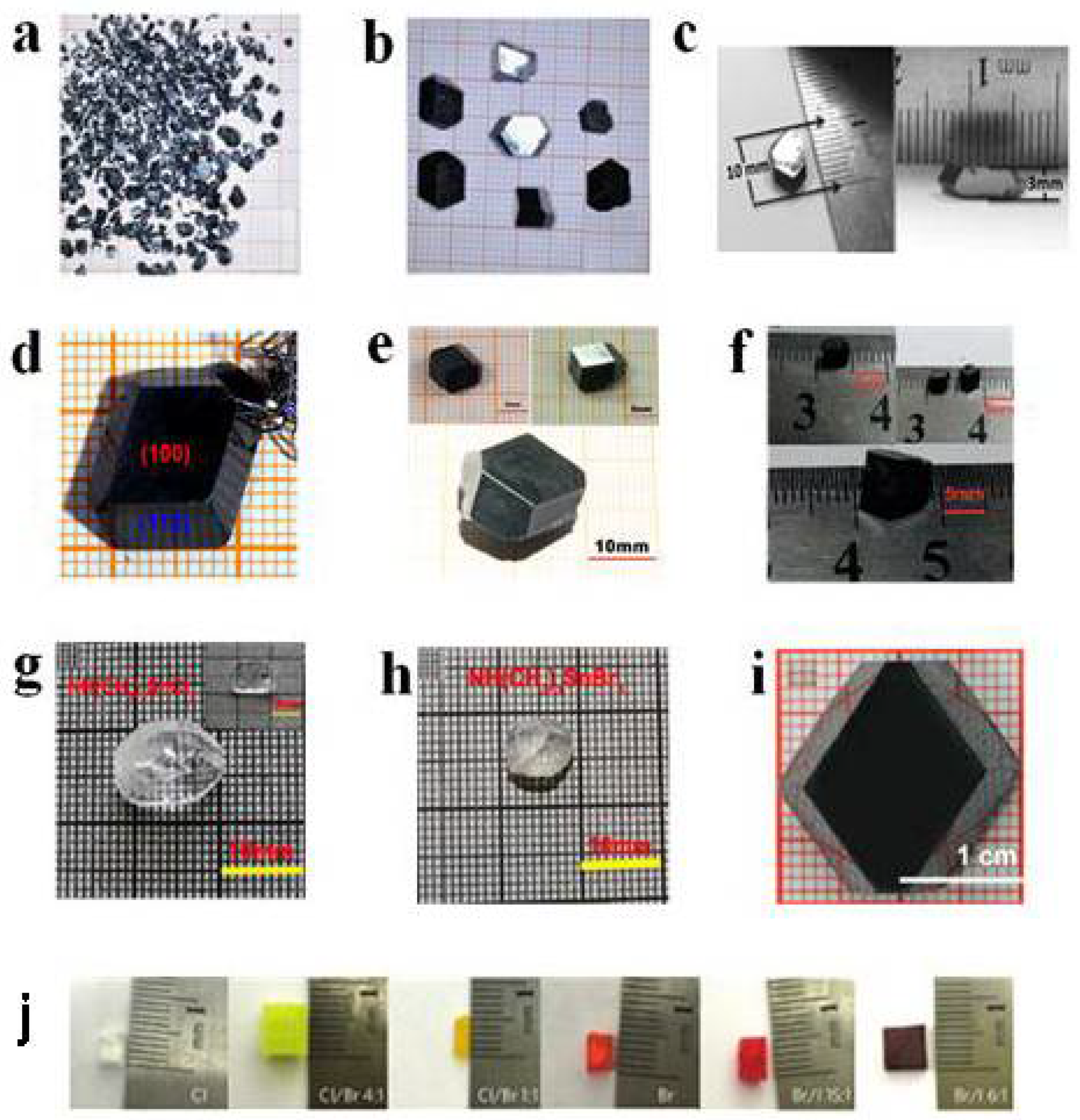
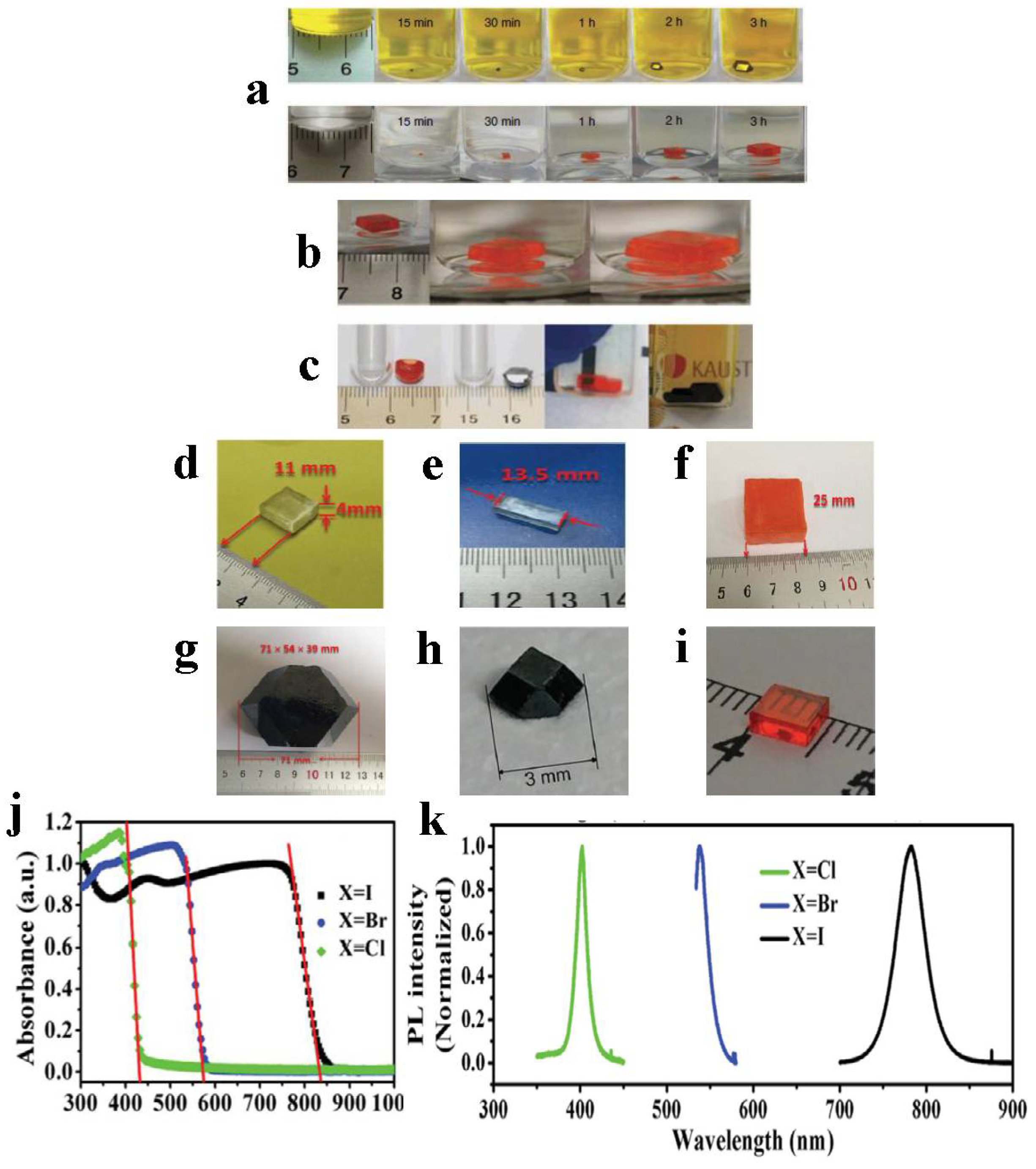
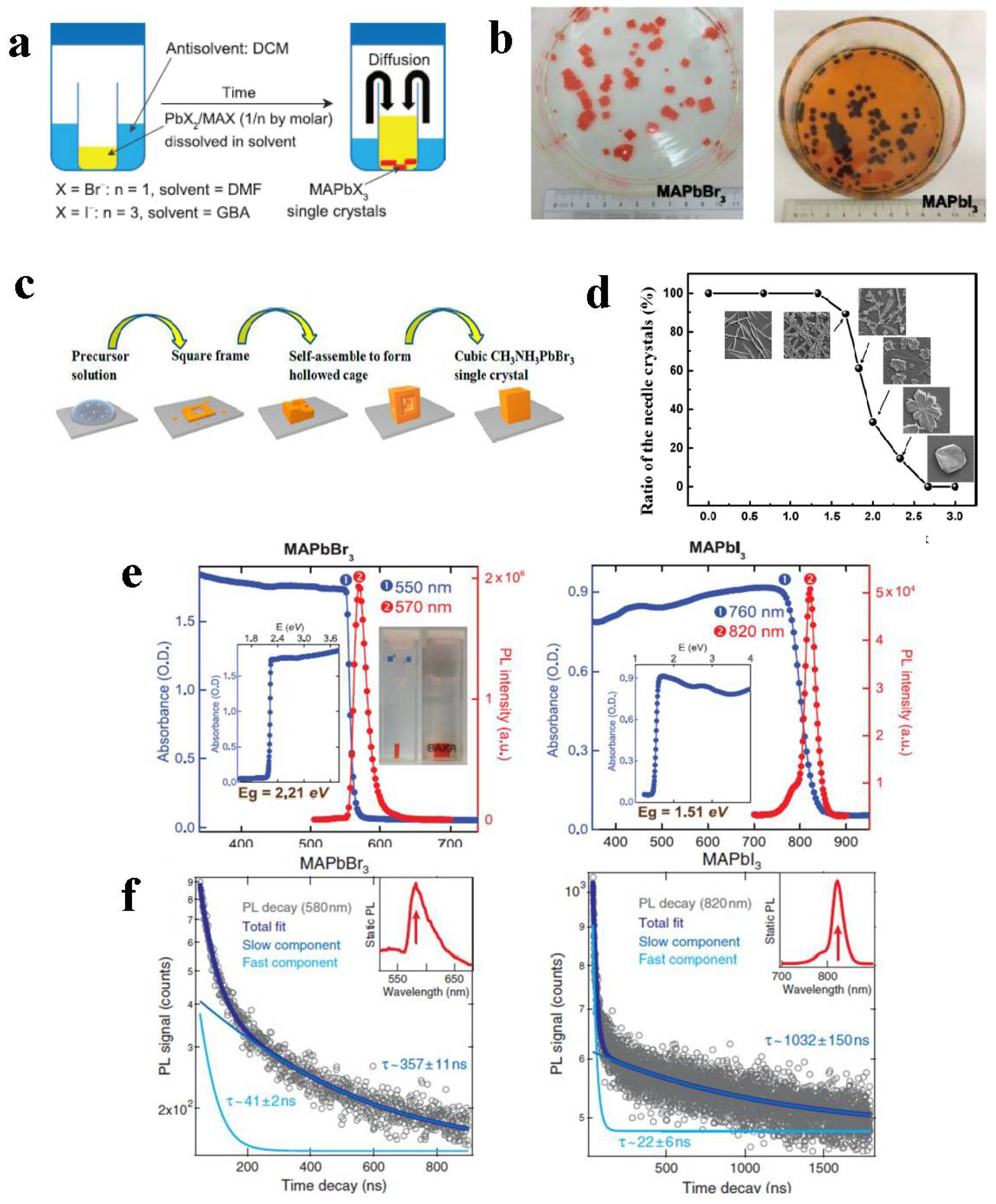
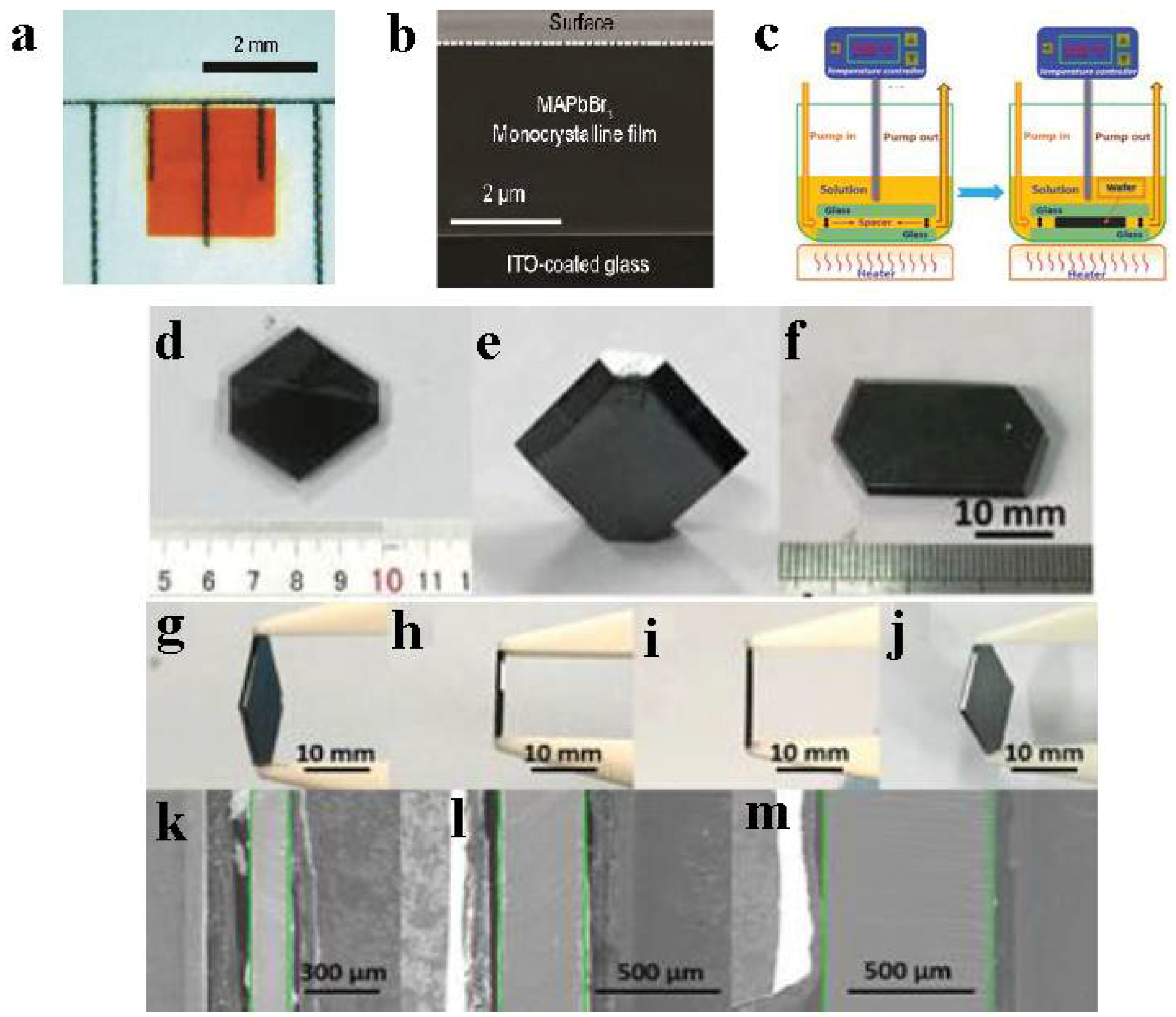
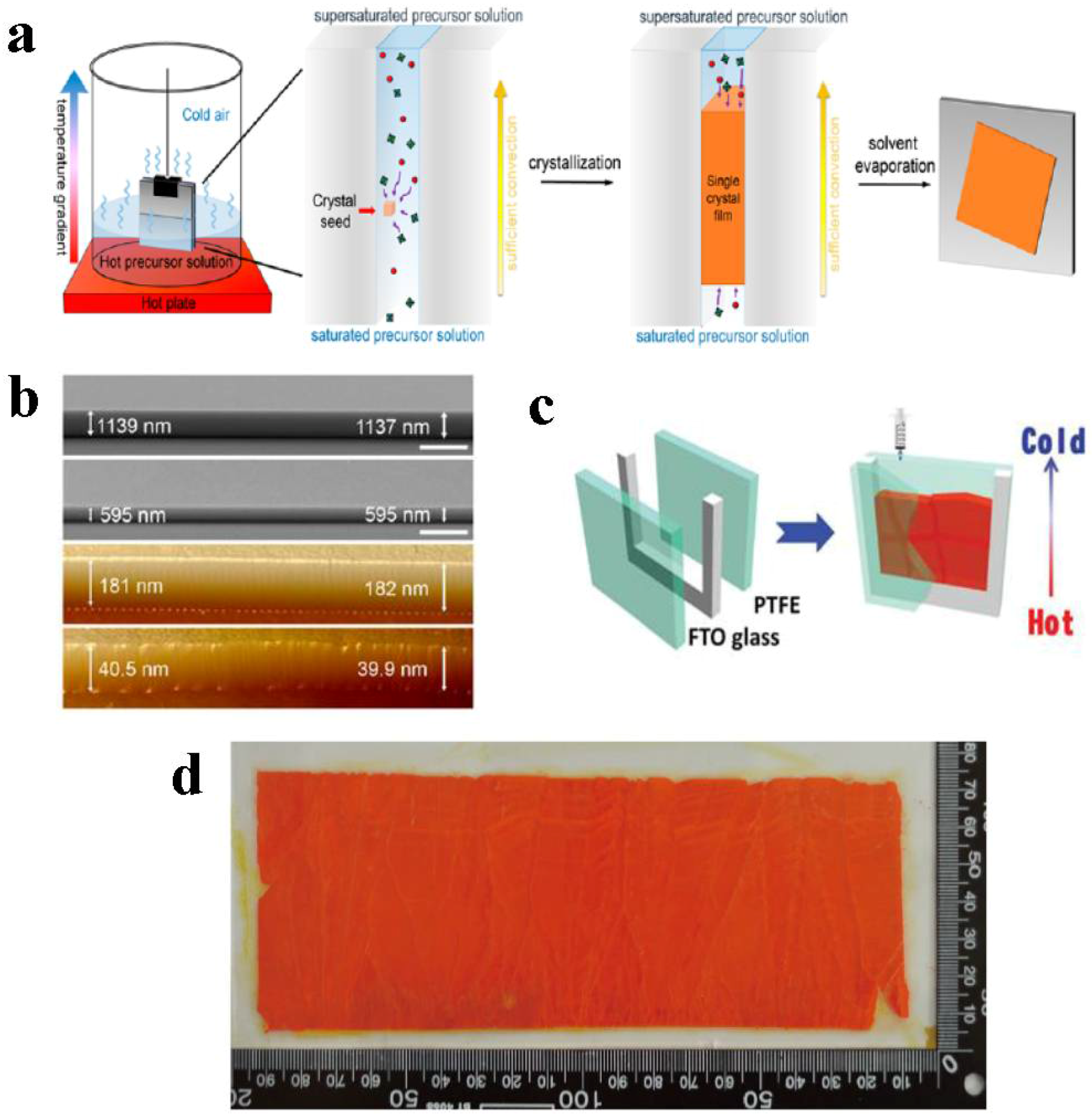
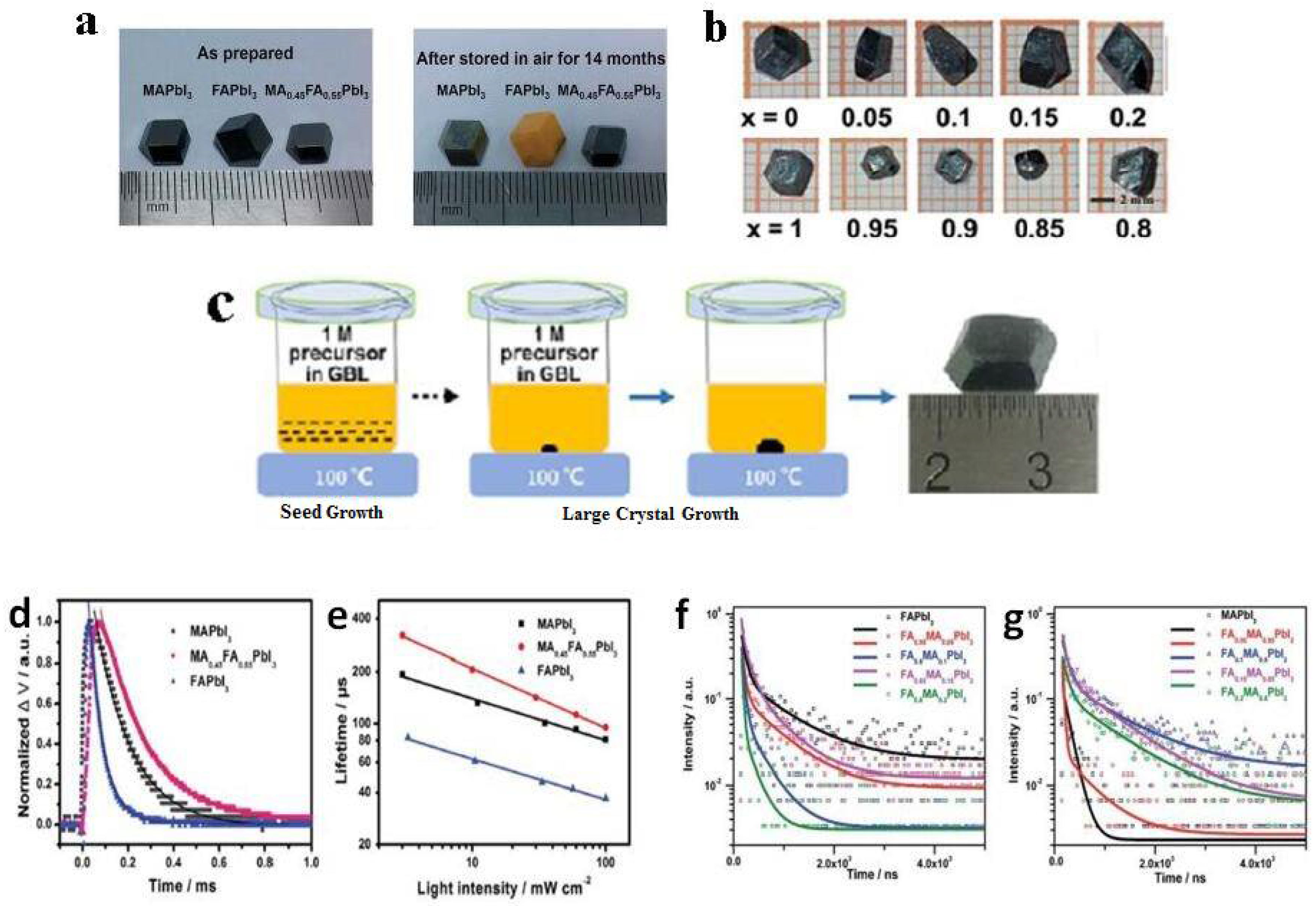
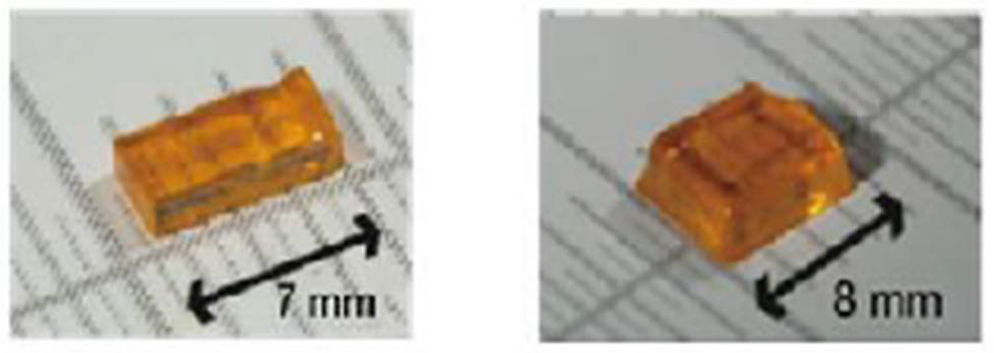
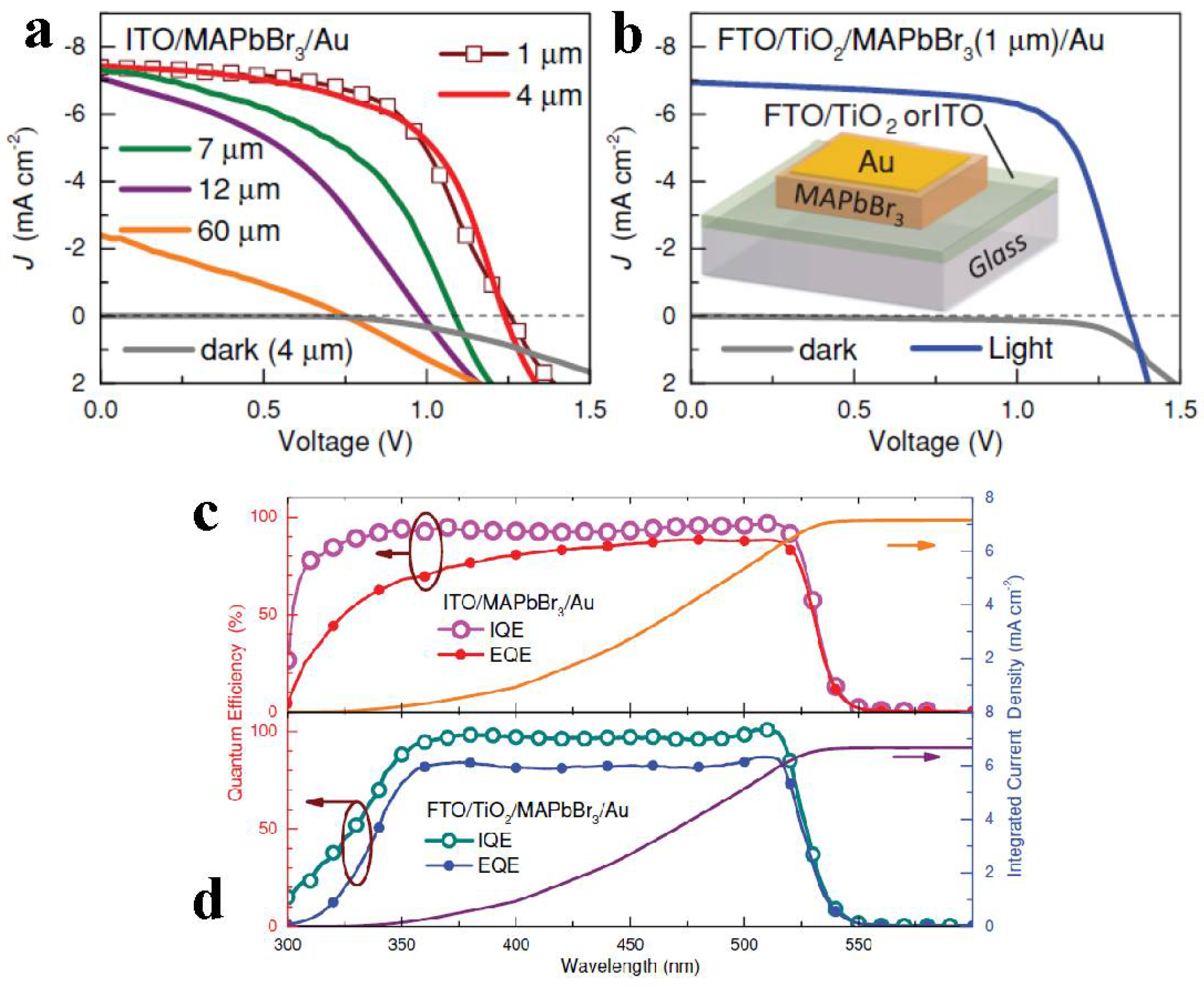
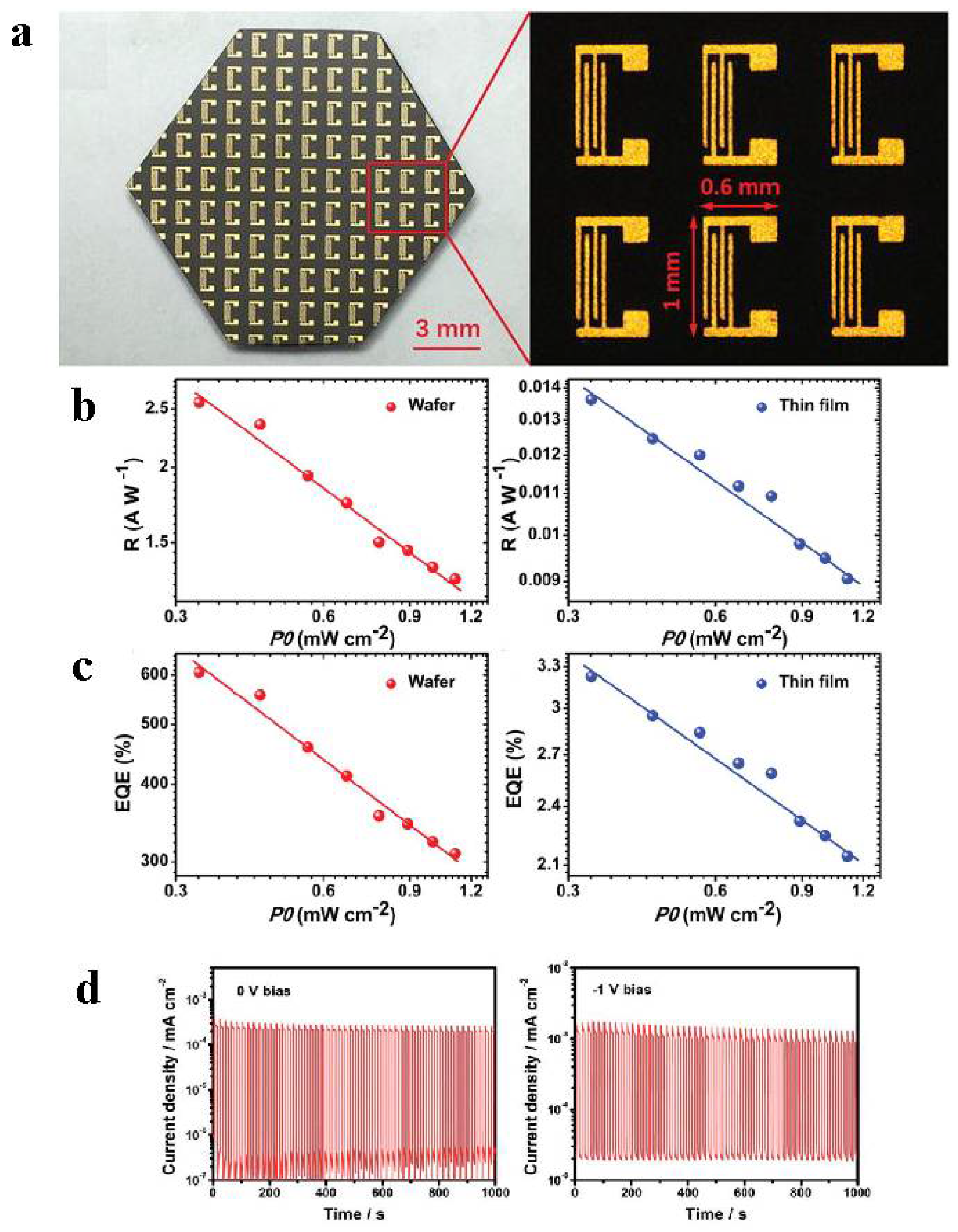
Table 1.
Lifetimes extracted from the PL spectra of FA(1−x)MAxPbI3 single crystals with x = 0, 0.05, 0.1, 0.15, 0.2, 0.8, 0.85, 0.9, 0.95, 1.
Table 1.
Lifetimes extracted from the PL spectra of FA(1−x)MAxPbI3 single crystals with x = 0, 0.05, 0.1, 0.15, 0.2, 0.8, 0.85, 0.9, 0.95, 1.
| FA(1−x)MAxPbI3 | x = 0 | x = 0.05 | x = 0.1 | x = 0.15 | x = 0.2 |
| τ1 (ns) | 91.26 | 61.43 | 52.11 | 27.26 | 31.58 |
| τ1 (ns) | 839.31 | 689.92 | 381.86 | 579.75 | 236.74 |
| FA(1−x)MAxPbI3 | x = 1 | x = 0.95 | x = 0.9 | x = 0.85 | x = 0.8 |
| τ1 (ns) | 7 | 32.45 | 122 | 88.05 | 105.3 |
| τ1 (ns) | 145.65 | 557.5 | 1074.78 | 926.39 | 956.8 |
Table 2.
Summary of perovskite single crystal growth methods and properties of as-grown crystals.
| Single Crystal | Growth Method | Size (mm) | Growth Period | Properties | Ref. | |
|---|---|---|---|---|---|---|
| Carrier Mobility (cm2·V−1·s−1) | Trap State Density (cm−3) | |||||
| MAPbI3 | STL | 2–3 | 48 h | [60] | ||
| CH3NH3PbBr3 | 5 | More than 10 days | [60] | |||
| MAPbI3 | 10 × 10 × 8 | [61] | ||||
| MAPbI3 | 12 × 12 × 7 | 2–4 weeks | 105 ± 35 | 1010 | [62] | |
| MAPbI3 | 20 × 18 × 6 | 5 days | [63] | |||
| CH3NH3 PbI3 (Cl) | 20 × 18 × 6 | 5 days | 167 ± 35 | 7.6 × 10⁸ | [66] | |
| MAPbI3 | ITC | 71 × 54 × 39 | 34 | 1.4 × 10¹⁰ | [71] | |
| MAPbCl3 | 7 | 3 days | 179 | 1.8 × 10⁹ | [71] | |
| MAPbBr3 | 11 × 11 × 4 | 4.36 | 2.6 × 10¹⁰ | [71] | ||
| FPbI3 | 5 | 4.4 | 1.5 × 10¹¹ | [76] | ||
| MA0.45FA0.55PbI3 | 8 | 4 h | 271 ± 60 | 2.6 × 10⁹ | [86] | |
| CH3NH3PbBr3 | AVC | 1.4 × 1.4 × 0.7 | 109–1010 | [78] | ||
© 2018 by the authors. Licensee MDPI, Basel, Switzerland. This article is an open access article distributed under the terms and conditions of the Creative Commons Attribution (CC BY) license (http://creativecommons.org/licenses/by/4.0/).
Share and Cite
MDPI and ACS Style
Li, S.; Zhang, C.; Song, J.-J.; Xie, X.; Meng, J.-Q.; Xu, S. Metal Halide Perovskite Single Crystals: From Growth Process to Application. Crystals 2018, 8, 220. https://doi.org/10.3390/cryst8050220
AMA Style
Li S, Zhang C, Song J-J, Xie X, Meng J-Q, Xu S. Metal Halide Perovskite Single Crystals: From Growth Process to Application. Crystals. 2018; 8(5):220. https://doi.org/10.3390/cryst8050220
Chicago/Turabian StyleLi, Shuigen, Chen Zhang, Jiao-Jiao Song, Xiaohu Xie, Jian-Qiao Meng, and Shunjian Xu. 2018. "Metal Halide Perovskite Single Crystals: From Growth Process to Application" Crystals 8, no. 5: 220. https://doi.org/10.3390/cryst8050220
Note that from the first issue of 2016, this journal uses article numbers instead of page numbers. See further details here.