Review

In2O3-Based Thermoelectric Materials: The State of the Art and the Role of Surface State in the Improvement of the Efficiency of Thermoelectric Conversion

by
Ghenadii Korotcenkov
1,*,
Vladimir Brinzari
2,* and
Moon-Ho Ham
1,*
1
School of Materials Science and Engineering, Gwangju Institute of Science and Technology, Gwangju 61005, Korea
2
Department of Theoretical Physics, State University of Moldova, Chisinau 2009, Moldova
*
Authors to whom correspondence should be addressed.
Crystals 2018, 8(1), 14; https://doi.org/10.3390/cryst8010014
Submission received: 9 October 2017 / Revised: 1 November 2017 / Accepted: 6 November 2017 / Published: 1 January 2018
(This article belongs to the Special Issue Semiconductor Nanomaterials Surfaces)

Abstract

:
In this paper, the thermoelectric properties of In2O3-based materials in comparison with other thermoelectric materials are considered. It is shown that nanostructured In2O3 Sn-based oxides are promising for thermoelectric applications at moderate temperatures. Due to the nanostructure, specific surface properties of In2O3 and filtering effects, it is possible to significantly reduce the thermal conductivity and achieve an efficiency of thermoelectric conversion inaccessible to bulk materials. It is also shown that a specific surface state at the intergrain boundary, optimal for maximizing the filtering effect, can be achieved through (1) the engineering of grain boundary parameters, (2) controlling the composition of the surrounding atmosphere, and (3) selecting the appropriate operating temperature.

1. Introduction

There is a huge amount of waste heat, such as the heat from the cars, different technological processes and human activities, which can be converted into useful energy, helping to increase production efficiency and improve living conditions [1,2,3,4,5,6]. Therefore, the development of different types of energy conversion technologies, including thermoelectric energy conversion, is currently one of the most pursued directions of research. Thermoelectric (TE) power generation is based on the Seebeck effect, which concerns the generation of the electromotive force (voltage) between the two ends of a solid bar under a certain temperature difference. When the electric circuit is connected to this solid, the electric current flows through the circuit to generate electric power, and thus heat can be converted into electricity. In contrast to other energy conversion technologies, thermoelectric power generation and thermoelectric cooling have many desirable properties, such as no moving parts, simple configuration, maintenance-free operation for thousands of hours, adaptability for any temperature range, no scaling effect from milliwatt to kilowatt ranges, etc., to make a potential contribution towards reducing greenhouse-gas emissions and providing a cleaner form of energy [4,7,8,9,10,11,12,13].
It is clear that the field of application of this or that energy conversion technology depends on the conversion efficiency. This means that the energy conversion efficiency is the most important parameter of these technologies [7,14]. Therefore, the main objective of most studies carried out in the field of thermoelectrics was to improve the efficiency of thermoelectric conversion.
As it is known [15,16], the conversion efficiency (η) is usually expressed through the dimensionless factor of merit ZT, which is linearly dependent on the temperature:
Z T = α 2 σ · T k = P F · T k
where α is the Seebeck coefficient; σ the conductivity; κ the coefficient of thermal conductivity; T the absolute temperature; and PF is a power factor, an electric component of thermoelectric conversion efficiency. Assuming a negligible contact resistance and optimized load condition, the maximum conversion efficiency of TE power generation, η, is expressed as Equation (2)
𝜂 = ( T h o t T c o l d T h o t ) [ 1 + Z T m 1 1 + Z T m + ( T c o l d T h o t ) ]
where the Carnot efficiency is given as the ratio of the temperature difference between the hot-end temperature and the cold-end temperature (ThotTcold), to Thot, and Tm is the mean temperature. The dependence of conversion efficiency on the temperature difference (ThotTcold) for different ZT values is shown in Figure 1. This indicates that the value of ZT for any thermoelectric material should be at least equal to one for an achievement efficiency acceptable for its practical application.
As it follows from Equation (1), the materials designed for thermoelectric applications should have a variety of conflicting properties [17]. To maximize the thermoelectric figure of merit (ZT) of a material, this material should have the following set of parameters: (1) a large thermopower (absolute value of the Seebeck coefficient, S > 100 μV/K), needed to obtain a high voltage, (2) high electrical conductivity (ρ < 10−2 Ω·cm), required to reduce the internal resistance of the material, and (3) low thermal conductivity (k < 1 W/m·K), necessary to introduce a large temperature difference into both ends of the material [18,19]. As these transport characteristics depend on interrelated material properties, a number of parameters need to be optimized to maximize ZT. For example, a low concentration and heavy effective mass of charge carriers contributes to the improvement of the Seebeck coefficient (Equation (3)). However, a heavy effective mass and low carrier concentration are not advantageous for electrical transport properties, because in this case the electrical conductivity will be low. To achieve maximum conductivity, it is necessary to have a maximum concentration of carriers with high mobility. However, as is known, materials with large effective masses have a low mobility of carriers. In addition, an increase in the carrier concentration to the required value provides a sharp decrease in the mobility of charge carriers in addition to a decrease in S [20]. For In2O3, such dependences are shown in Figure 2 and Figure 3.
S = 8 π 2 k B 2 T 3 q h 2 m d * ( π 3 n ) 2 / 3
where S is the Seebeck coefficient, kB is the Boltzmann constant, T is the absolute temperature, q is the electron charge, h is the Plank constant, md* is the effective mass at the Fermi level, and n is the electron concentration (for n-type conductivity).
In addition, to ensure that the Seebeck coefficient is large, there should only be a single type of carrier. Mixed n-type and p-type conduction will lead to moving the part of charge carriers to the cold end, decreasing the induced Seebeck voltage. The design of the materials also conflicts with the necessity for low thermal conductivity. Thermal conductivity in thermoelectrics comes from two sources: (1) electrons and holes, transporting heat (κe), and (2) phonons, travelling through the lattice (κl). Most of the electronic term (κe) is directly related to the electrical conductivity through the Wiedemann–Franz law:
k = k e + k l
and
k e = L 𝜎 T = n e μ L T
where L is the Lorenz factor. As high ZT requires high electrical conductivity, but low thermal conductivity, the Wiedemann–Franz law reveals an inherent material conflict for achieving high thermoelectric efficiency. Materials with high conductivity cannot have an extremely low thermal conductivity. As for the lattice thermal conductivity, which is controlled through the transport of phonons, there are also limitations. It is difficult to provide a strong scattering of phonons without significantly affecting the mobility of the main charge carriers, i.e., electrical conductivity. Thus, thermoelectrics requires rather unusual materials. This means that the search for optimal materials for thermoelectric converters is indeed a difficult task.

2. How to Improve the Conversion Efficiency and Why Metal Oxides Can Be Used for This?

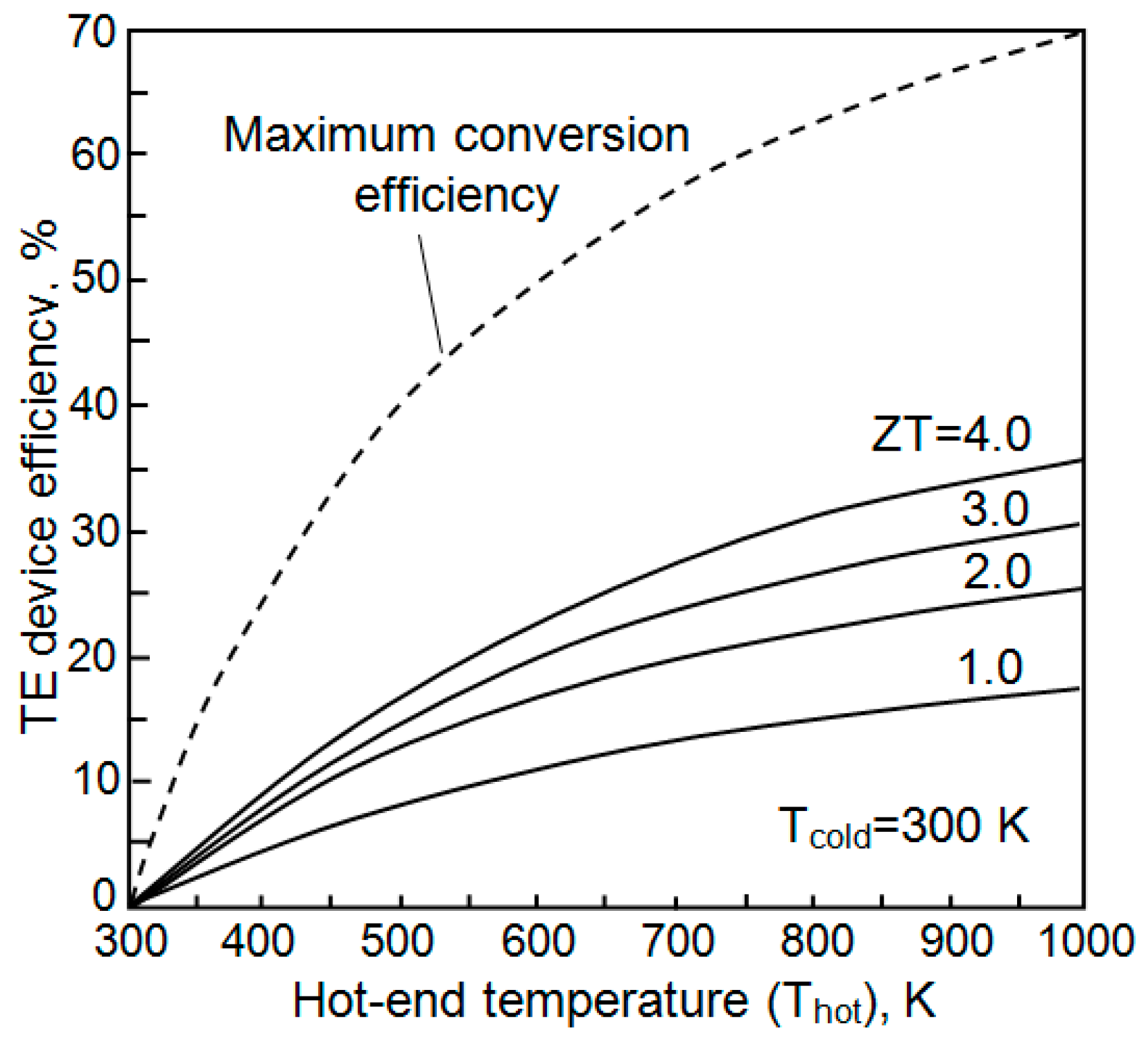
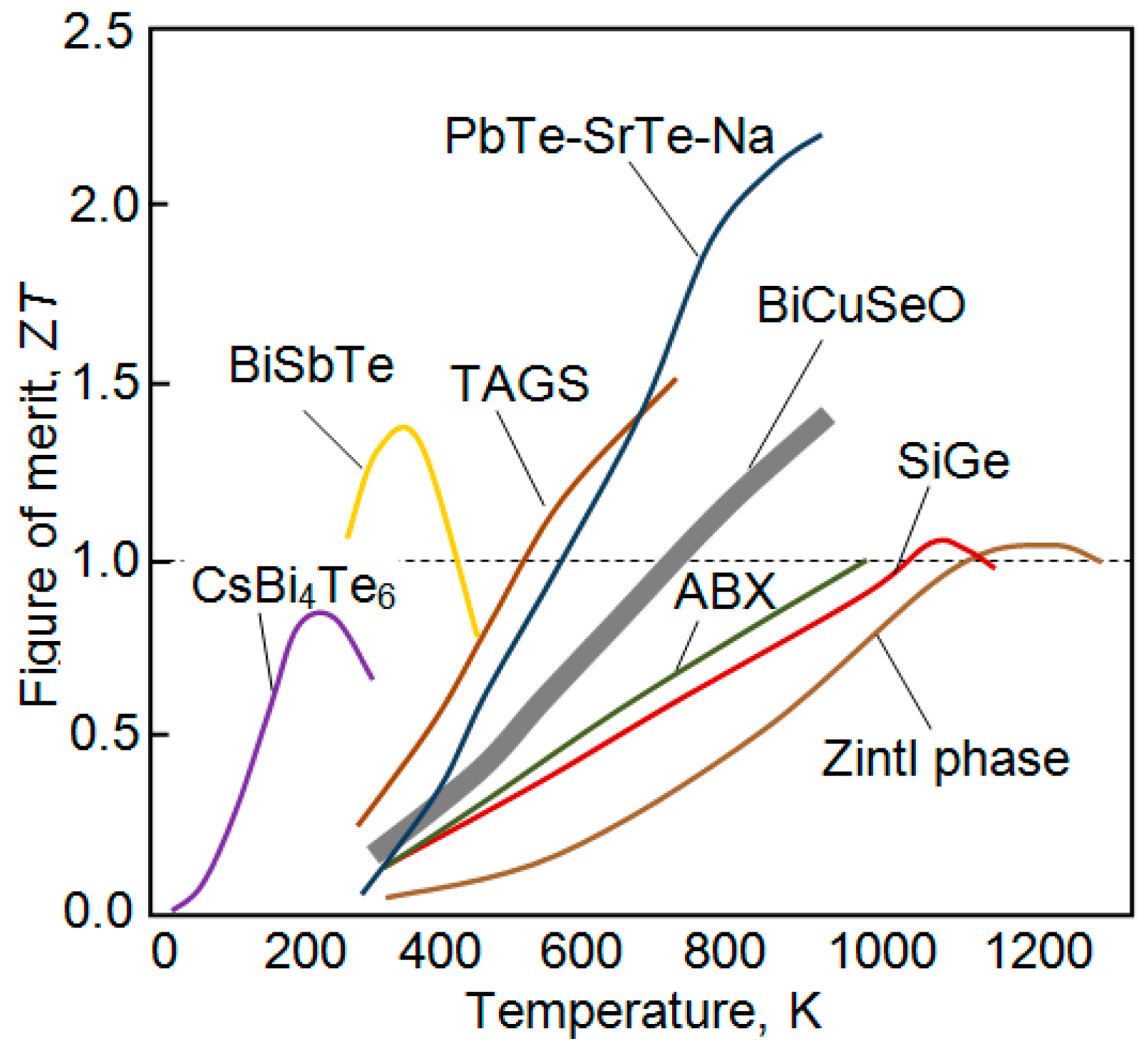
2.1. Increase in Operating Temperatures

If we look at Equation (1), then it follows from this, that an increase in operating temperature is the easiest method to increase ZT. Thermoelectric materials such as PbTe, BiSbTe, Bi2Te3, CoSb3, Zn4Sb3, CsBi2Te3, AgSbTe2, Cu2Se1.01, SnSe, AgPb18SbTe20, and Na0.95Pb20SbTe22 [17,22,23,24,25] show the highest figure of merit ZT (see Figure 4). For instance, Bi2Te3/Sb2Te3 superlattices have an extraordinary ZT of 2.4 at 300 K [26]. However, these materials are composed of toxic, naturally rare, and heavy elements and can easily decompose, vaporize, melt or be oxidized at high temperatures in air. Thus, these conventional TE materials cannot be employed for extensive applications for waste heat recovery in an air atmosphere [14]. For example, Bi2Te3 material is not suitable for application when the temperature is higher than 250 °C. PbTe material is harmful to human body and may cause environmental pollution. As a result, the practical utilization of the above-mentioned thermoelectric materials as power generators has been limited and the search for materials with thermoelectric parameters capable of operating at high temperatures continues to be of great interest. Experiments have shown that metal oxides are suitable materials for solving this problem [14,27,28,29,30,31,32,33,34].
As compared with conventional thermoelectric materials, such as PbTe, Bi2Te3, etc., conductive metal oxides have considerably better chemical and thermal stabilities, and therefore they are able to operate at temperatures above 1000 °C. Thus, the increase of working temperature for improving the parameters of thermoelectric generators, such as heat engines, can be realized using these materials. Compared with traditional TE materials, metal oxides are not only thermo- and chemically stable in the air at high temperatures, but many of them also have wide band gaps (Eg ≥ 3.1 eV). As a result, the minority carrier concentration will always be negligible and therefore the figure of merit (ZT) should continue to increase with increasing operating temperature in linear mode, if other parameters are unchanged. The high chemical and thermal stability of oxides also allows for a large temperature gradient to be applied across the materials in the air, thereby leading to a high Carnot efficiency in Equation (2) that somewhat compensates for the low ZT. In addition, the large temperature gradient may induce novel nonlinear, nonlocal TE effects (e.g., the Benedicks effect [36] that may be thermoelectrically favorable [37]. The increase in the operating temperature is also accompanied by the increase in electroconductivity and a decrease in the thermal conductivity of metal oxides [38,39,40]. These changes should lead to a further increase in ZT. Finally, the most oxides are decidedly advantageous in terms of the cost of raw materials and the environmental friendliness.
Silicon-germanium alloys [41] and transition metal silicides such as Mg2Si [42], FeSi2 and MnSi [43] can also operate at increased temperature. However, this temperature range is limited and these materials should be protected from the effects of oxygen and aggressive gases. In addition, the ZT of these materials is less than 1.0 [29]. In particular, the ZT for the Si-Ge alloys is fairly low because of their relatively high lattice thermal conductivity [8].
At present, among the metallic oxides, p-type oxides such as the layered cobalt oxides, NaCo2O4 (NaxCoO2), exhibit the highest figure of merit value: Z (~1 × 10⁻³ K−1) and ZT ~ 1 at T = 1000 K [22,44] and ~1.2 at 800 K [45]. As it was indicated before, materials with a ZT value exceeding one are, in general, considered as acceptable for thermoelectric applications. These results strongly suggest that NaCo2O4 is a promising candidate for a thermoelectric oxide. Another fascination of NaCo2O4 is the existence of various related oxides [46]. Metal oxides such as NaCo2O4, Ca3Co4O9 [19,47], (Bi,Pb)2Sr2Co2O9 [48], TlSr2Co2Oy [49], (Hg,Pb)Sr2Co2Oy [50], (Na1−yMy)xCo2O4 [51], and YbBaCo4O7 [18] have been found to show good thermoelectric performance. Moreover, some of these oxides are found to be as good as NaxCoO2. In particular, Funahashi et al. [52] showed ZT > 1 at 1000 K for a Bi-doped Ca3Co4O9 whisker crystal. Motohashi et al. [53] have found unusually large thermopower in Na1.5Co2O4. Terasaki et al. [54] found the Cu substitution enhanced the thermopower of NaCo2O4 without increasing resistivity. Even ZT > 2 was suggested in the Ca–Co–O system [52].
The reason for these electronic and thermoelectric properties of NaxCoO2 is still under debate. According to Terasaki [55], NaCo2O4 (NaxCoO2) has indicated thermoelectric characteristics due to the layered structure. The layered structure works quite well in two ways. One is that the electric current and the thermal current flow on different paths in space. This enables us to control the lattice thermal conductivity by properly choosing the insulating block layer. This is a manifestation of electron crystal and phonon-glass, and we call this type of material design “nano-block integration”. The other way is that the CdI2-type CoO2 block favors the low spin state of Co3+ and Co4+, which holds a large thermopower at high temperatures. In the case of the perovskite cobalt oxide R1−xMxCoO3 (R = rare-earth, M = alkaline earth), the high spin state of Co3+ seriously suppresses the thermopower. At the same time Maignan et al. [18] believe that for structures containing corner-shared Co2+/3+ tetrahedra, the present mixture of high spin Co2+ and Co3+ yields a significant upward shift of S at high temperatures. According to Maignan et al. [18], the cobalt magnetic network is frustrated with alternating Kagomé and triangular layers. This creates a disorder detrimental for the phonon propagation. As a result, low κ values (κ < 0.5 W/K·m for T < 300 K) can be observed. This result clearly indicates that the lattice frustration is a good component for controlling the thermal conductivity. With regard to the stability of these oxides, it was found that NaxCoO2 decomposes into insulating Co(OH)2 in a high humidity environment, because the Na+ ions easily dissolve in H2O, whereas Ca3Co4O9 exhibits good p-type TE properties and good thermal stability at 1000 K in the air [30].
Another promising material of p-type conductivity is BiCuSeO, an interest in which has appeared recently [33]. BiCuSeO oxyselenide [35,56,57,58,59,60,61] has been reported to exhibit low intrinsic thermal conductivity (~0.40 W/m·K at 923 K) and tunable electric properties; its highest ZT can be 1.4 at 923 K [57]. The very low thermal conductivity and high Gruneisen parameter [62] value of 1.5 in the BiCuSeO system are partially attributed to the increased bond anharmonicity, associated with the occurrence of trivalent Bi [63,64]. Combined with the analysis of the Young’s modulus and Gruneisen parameter for the BiCuSeO system, other possible reasons for high ZT include the layered structure, since phonons can be confined to the layers and scattered at the layer interfaces [26]. The presence of heavy elements also leads to lower group velocity for the phonons [65]. It was established that BiCuSeO comprises (Cu2Se2)2− layers alternately stacked with (Bi2O2)2+ along the c axis of a tetragonal cell [66,67]. The (Bi2O2)2+ layers act as a charge reservoir, and the conductive (Cu2Se2)2− layers provide a conduction pathway for the carrier transport. However, the ZT of oxychalcogenides is restricted by their electrical resistivity. The low electrical conductivity is related to a low carrier concentration of 1 × 1018 cm−3 and a carrier mobility of 22 cm2/V·s [68].
In contrast, n-type oxides, demonstrating high TE performance comparable to p-type oxides, have not yet been developed, despite continuing efforts [18,33,69]. Figure 5 shows the best results obtained during the last decades. It can be seen that as a result of these studies, that it was possible to substantially increase the ZT of n-type oxides. However, devices based on n-type conductive metal oxides have until now had a low efficiency of thermoelectric conversion [28,31,38,39,40,42,70,71], which made their utilization in thermoelectric generators economically unprofitable. The demand for a good n-type thermoelectric oxide proceeds from the fact that it usually is being utilized as a partner for a p-type material in thermoelectric modules. As is known, both p-type and n-type solid materials are required to fabricate a TE module [7].

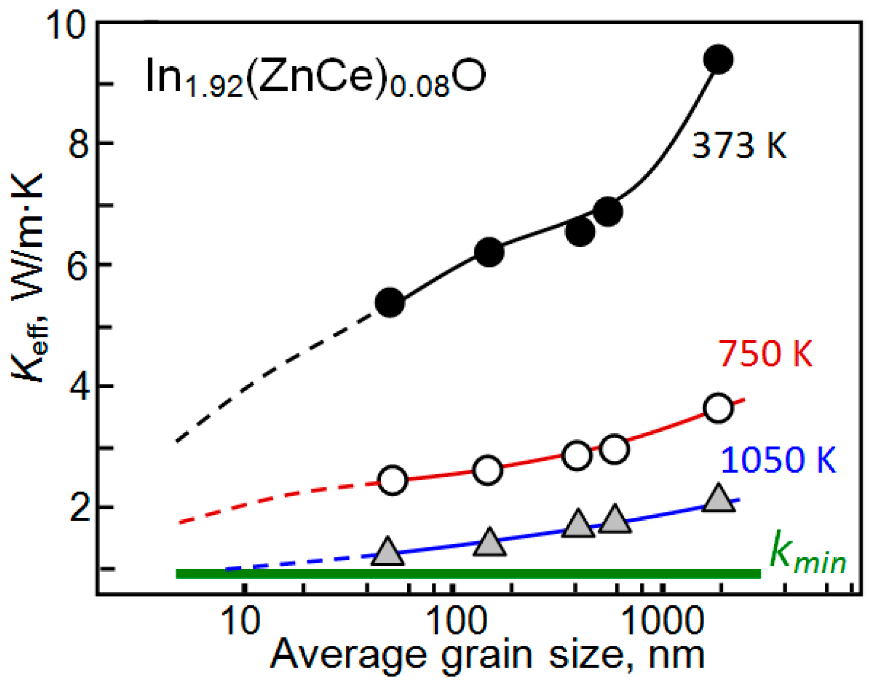
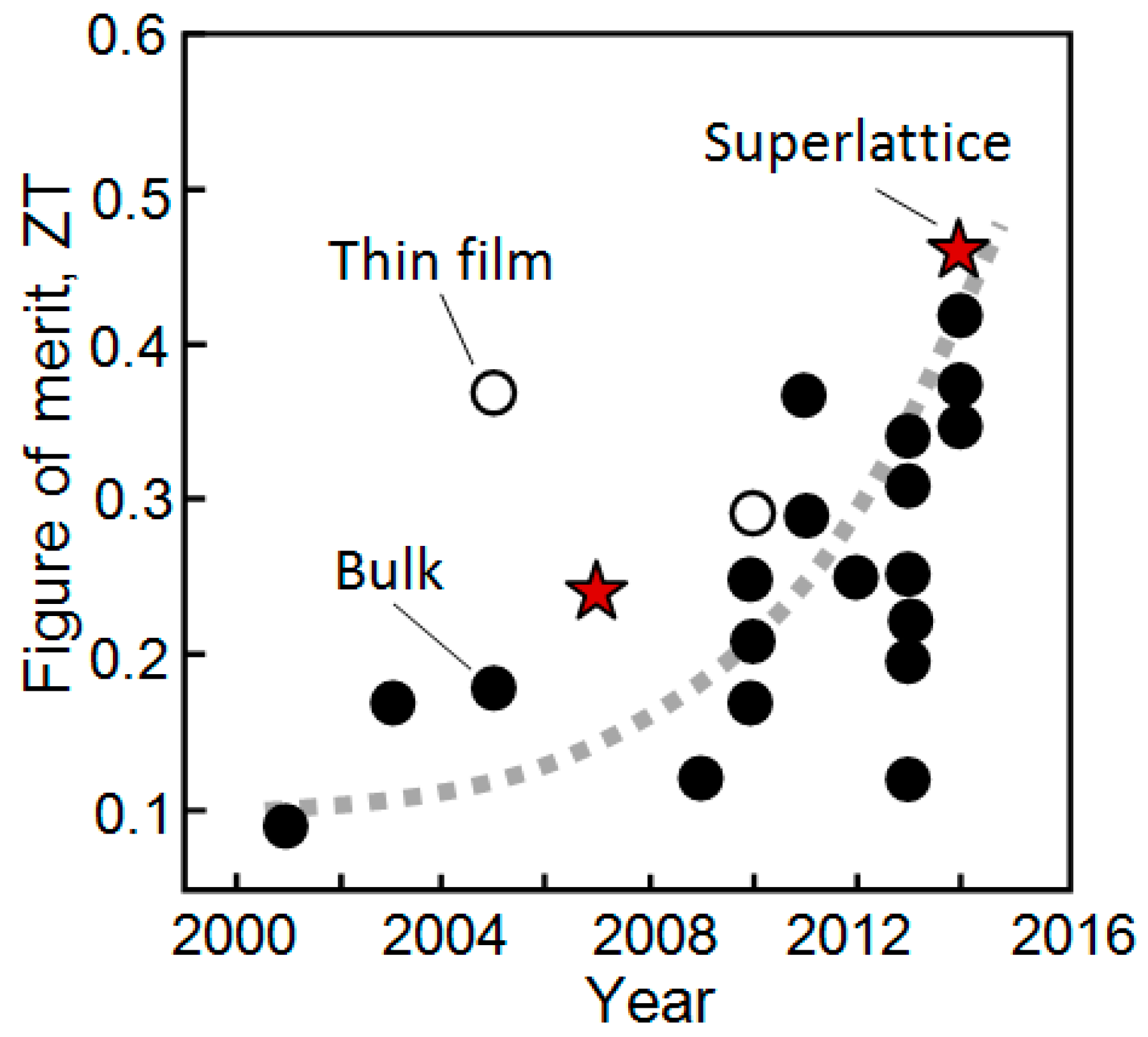
2.2. Nanostructuring

Experimental studies and theoretical calculations have showed that there is another fundamental possibility to increase ZT [14,33,38,72,73,74,75,76,77,78]. It was found that by exploiting nanoscale effects, nanostructured materials were able to improve their thermoelectric properties and increase ZT up to values that could not be achieved in traditional bulk materials [14,23]. It was established that in low-dimensional materials, the increase in ZT may come through a combination of two mechanisms: (1) a reduction in the lattice thermal conductivity due to the scattering [73], or the refraction [74] of phonons at the physical boundaries of the nanoscale structure, and (2) an increase in the power factor PF, or at least the avoidance of a decrease in the power factor with the decrease in κ. The last effect can be achieved through size quantization in the structures with lower dimensionality (1D and 2D structures) or through the energy filtering of the electrons involved in the charge transport [72,75]. In other words, the enhancement of ZT could be due to a large decrease of thermal conductivity without incurring a considerable decrease in the thermopower and electrical conductivity. The increase in phonon scattering can be achieved through the use of the introduction of rattling centers, mass fluctuation [79], grain boundaries [80], complex crystal structures [17], or nanocomposites [81]. The main issue of these material modifications is to introduce a scattering technique, minimizing electron scattering and maximizing the scattering of all-length-scale heat carrying phonons [82]. One should note that the use of metal oxides makes it possible to realize all these approaches. Oxides are featured by their chemical versatility and structural intricacy, which offers a great flexibility of structural and compositional tailoring [30]. In addition, the existing technology of nanostructured material synthesis with the required parameters is quite simple and cheap.

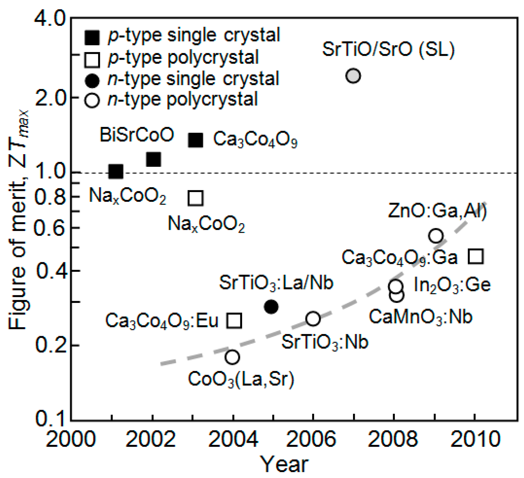
3. n-Type Oxides Promising for Thermoelectric Applications

At present, a sufficiently large number of different metal oxides have been tested as n-type thermoelectric materials [31]. Koumoto et al. [14] and Ohta [83] believe that the most promising candidates for n-type oxide TE materials are perovskite-type CaMnO3 [84] and strontium titanate (SrTiO3, or STO) [85]. These oxides can become semiconducting by suitable doping and these materials can exhibit a rather large S, which is comparable to that of a practical Peltier material, Bi2Te3 [34]. Electron-doped CaMnO3 and SrTiO3 have a large ZT not only because of their relatively high electrical conductivity, but also the large Seebeck coefficient, induced by their high carrier mobility, large effective mass and low thermal conductivity [29]. The total thermal conductivity of the sub-microcrystalline CaMnO3 and SrTiO3-based compounds is very low compared to the values reported for similar compounds [86]. This observation can be related to the small crystallite size and microstructure of the powders leading to a reduction in the lattice conductivity. For example, the manganate samples show total thermal conductivities between 1.0 and 1.5 W/m·K depending strongly on the crystallite size [29]. Furthermore, because the melting point of these oxides is very high, electron-doped crystals may be applicable at high temperatures (~1000 K). However, because Ti3+ ions are not very stable in STO, they become easily oxidized to Ti4+ above ~400 °C in the air, and the crystal becomes insulating. Mn3+ is more stable than Ti3+, so the doping reaction can proceed even in the air, and the generated Mn3+ ions can behave stably as donors at high temperatures. Accordingly, CaMnO3 can be applied as an n-type material to high-temperature waste heat recovery in the air, whereas STO can be used only for medium-temperature (300–600 K) applications, although both materials reveal only low ZT at the moment.
At present, the maximum ZT value, which was achieved in a 20% Nb-doped sintered STO (20% Nb-STO) film, was no higher than 0.37 at 1000 K [87]. For the conventional STO-based materials mentioned above, a great effort to reduce κ by heavy electron doping and isovalent substitution in single-crystal and polycrystalline ceramics has also not led to a satisfactory suppression of heat transport because of insufficient phonon scattering. The use of a STO/SrTi0.8Nb0.2O3/STO or STO/STNO/STO superlattice, which was fabricated on the (001) face of a LaAlO3 single-crystal substrate by pulsed laser deposition technique, yielded some improvement in conversion efficiency [88]. However, from the viewpoint of practical applications, superlattice thin films are not suitable, because the technology is complicated and expensive. At the same time, the study of nanostructured films showed that this approach, based on nanostructuring, makes it possible to achieve significant success. In particular, Koumoto’s group reported the incorporation of nanosized yttria-stabilized zirconia [89], mesoporous silica, [90] and potassium titanate [91] in the Nb-doped SrTiO3 bulk matrix and the impact on the TE properties. The results showed that these additions (up to a few wt %) enhanced the phonon scattering at grain boundaries, increased the electrical conductivity via promoting the packing density, thus leading to a substantial enhancement of ZT. An approach involving quantum nanostructured STO ceramics with optimized grain boundaries (GB) demonstrated by a simulation possibility to generate ZT ~ 0.8 at 300 K [14]. A reduction in κ by 45% as compared with a bulk single crystal, was achieved in a 55-nm grained ceramic sample due to enhanced phonon scattering at nanometer-scale GBs (see Figure 6). It can be seen that there is a substantial reduction in thermal conductivity as the grain size decreases, particularly at lower temperatures, at which the anharmonic phonon–phonon scattering effects are less significant, consistent with the expectations of the Debye model discussed above [92]. According to Ohta [83], the ZT at 300 K for nanostructured STO can be increased even up to 2.4. However, these values are not confirmed experimentally. Figure 7 shows a comparison of the ZT values of different SrTiO3-based thermoelectric materials that have been obtained over time.
Another group of promising n-type oxide materials for thermoelectric applications is formed by binary metal oxides such as ZnO, SnO2, TiO2, and In2O3, also known as transparent conducting oxides (TCOs) and transition metal oxides (TMOs) [2,17,22,31,33]. Interest in these materials is due to the fact that these metal oxides can show a wide range of electronic properties ranging from insulating to semiconducting and conducting [94]. In particular, transition metal oxides have strong electronic correlations and narrow d bands. Hence, strong spin and orbital fluctuations as well as high degeneracy can take place in these d-electron systems, which are advantageous for improved thermoelectric performance [95]. Moreover, their electronic properties can be engineered by changing their morphology, doping and stoichiometry. The phonon generation and propagation properties in many TCOs and TMOs are well-understood and molecular engineering methods have been developed for tuning them. Their abundance in nature is another important advantage for technologies to be widely adopted. Additionally, these metal oxides show a wide range of interesting thermal properties at cryogenic, ambient and high temperatures. Many TCOs and TMOs offer high Seebeck coefficients, with desired thermal and electrical conductivities and heat capacities, at targeted temperatures that can be exploited for different applications [69,96,97].
For example, an extremely large figure of merit (ZT = 1.64 at T = 1073 K) was reported by Okinaka and Akiyama [98] for non-stoichiometric TiO1.1; however, one should note that no other evidence has appeared after this publication. Usually, in the literature it is possible to find a ZT not exceeding 0.25–0.3 [99,100,101,102]. At that, as a rule, non-stoichiometric TiOx showed better thermoelectric characteristics. For example, Tsuyomoto et al. [103] have shown that TiOx (x = 1.94) with an orthorhombic crystal structure, exhibited a peak S of ~518 μV/K and σ of 20 S/cm at ~350 K. They demonstrated that both S and σ increased with temperature, resulting in a PF of ~0.54 mW/m·K2 at 343 K. Non-stoichiometric TiOx also had minimal thermal conductivity (0.83 W/m·K).
Another metal oxide, in which increased interest has been exhibited, was ZnO [33,34]. ZnO-based materials are an important class of TE oxides featured by high μ values on the order of 10–100 cm2/V·s [104] (one of the highest reported in oxides), high thermal stability, and high PFs of the order of 1 mW/m·K2 (comparable to that of SiGe materials) [105]. Due to its wide band gap, ZnO has no bipolar conduction. However, it also exhibits a high k (~40 W/m·K) [106]. Therefore, the main challenge in designing this material is to reduce kl without deteriorating the PF. One of the most effective methods for such optimization of metal oxides is the introduction of a second nanophase, which, on the one hand, will promote the growth of conductivity, and on the other will lead to a decrease in thermal conductivity. However, making a solid solution with MgO, NiO, Fe2O3 and Al2O3 has proved to be unsuccessful due to the insufficiently high carrier concentration in these solid solutions [104,107,108]. In particular, according to Tsubota et al. [104], the carrier concentration in ZnO:Al at optimum doping did not exceed 8 × 1019 cm−3. Doping was also not accompanied by a strong drop in thermal conductivity. Even at 1000 K, the thermal conductivity did not drop below 5 W/m·K [104]. As a result, Zn0.98Al0.02O had a power factor, S2·σ, and ZT equaled ~1.5 mW/m·K2 and 0.24–0.3 at 1000 K, correspondingly. Due to the very low dopant solubility on the Zn site, the addition of Al to ZnO of more than 2 mol% resulted in the formation of fine precipitates of ZnAl2O4 [104,107]. In the case of sintered ZnO:Fe ceramics, the thermoelectric parameters were even worse [108]. The ZT of ~2 × 10⁻² at 1073 K was only slightly above the values observed for undoped ZnO.
The doping of sintered ZnO with gallium also did not noticeably improve its thermoelectric characteristics [109,110,111]. Despite an increase in conductivity by almost two orders of magnitude to 1 S/cm and a decrease in thermal conductivity to 3.5 W/m·K, the figure of merit for the ZnO:Ga ceramics did not exceed 0.1 at 1000 K. In the case of ZnO:Ga (1%) films deposited by atomic layer deposition (ALD) [112], the conductivity can reach ~2 × 10³ S/cm. However, due to the low Seebeck coefficient, the maximum value of PF is only 0.85 mW/m·K2 at 330 K. Approximately the same thermoelectric parameters were obtained for sintered ZnO ceramics doped with indium [113,114,115,116,117,118,119]. When the concentration of In2O3 in ZnO was increased to 10 mol%, the thermal conductivity of ZnO:In decreased to ~1.6–2.0 W/m·K, and the ZT in samples with optimal doping reached values of ~0.1 at 1073 K. According to [109,116], the optimization of the thermoelectric parameters of metal oxides from the ZnO-In2O3 and ZnO-Ga2O3 systems is conditioned by the specificity of point defects [120,121,122], generated at low doping levels, and by the formation of Ga2O3(ZnO)m and In2O3(ZnO)m superlattice compounds in the Ga and In highly doped ZnO. Such superlattices belongs to the RMO3(ZnO)m type of homologous layered oxides [111,119,121,122,123]. In these compounds m is an integral number basically denoting the number of Zn-O layers between Ga–O layers. Exactly these multiple complex defects and nanoscale interfaces provide additional strong phonon scattering, leading to a drastic reduction in thermal conductivity in these ZnO-based compounds [109,116,118].
At the same time, Ohtaki et al. [124] reported that due to the co-doping of Al and Ga in ZnO, the ZT can be increased up to ~0.65 at 973 K. It was found that dual doping helps to improve the solubility of dopants in ZnO [125]. The nanocomposite synthesized by Ohtaki et al. [124] had a nominal composition of Zn0.96Al0.02Ga0.02O. These results were encouraging, but no further improvement in the efficiency of the thermoelectric conversion was observed. Of recent results, only the results reported by Jood et al. [126] and Wu et al. [127] can be distinguished. The Al-ZnO nanocomposites synthesized by Jood et al. [126] showed high σ and S, resulting in a significantly high PF and ZT of 0.9 mW/m·K2 and 0.44 respectively, at 1000 K. The same nanocomposites also had reduced values of k (1.5 W/m·K at 300 K). Approximately the same thermal conductivity was demonstrated by In2O3(ZnO)9 doped with Al [128]. This paper reported a two-fold reduction in the thermal conductivity and an improvement of about 170% in the Seebeck coefficient of an existing In2O3(ZnO)9 superlattice by chemically modifying the interface with small additions of aluminum. This research has shown that the superlattice interfaces can be chemically tuned for specific properties, which are important for applications in areas like thermoelectrics. Kosir et al. [129] also reported some improvement in the thermoelectric characteristics of (ZnO)5In2O3 after doping with aluminum. However, this improvement was observed only for small additions of Al (x = 0.01–0.05). The observed improvement was explained by the increased carrier mobility for a smaller number of charge carries and decreased the thermal conductivity. However, with a further increase in the Al additions, the charge-carrier concentration and their mobility dropped due to the disturbance of the main conduction paths of the InO2 layers exposed to the strain accompanying the structural shrinkage; these resulted in poor electrical conductivity and decreased ZT values for the (ZnO)5(In1−xAlx)2O3 ceramics in comparison to the undoped composition.
Wu et al. [127] have found that the presence of polyparaphenylene (PPP) nanoparticles in the Zn0.95Ni0.05O matrix was also effective in improving the ZT up to ~0.54 at 1173 K. This improvement was achieved due to an increased power factor and a reduction in thermal conductivity. However, the values of k for these nanocomposites did not drop below 2 W/m·K even at 1000 K. For most other studies, the ZT did not exceed 0.15–0.3 [130,131].
Information on other n-type oxides such as MnO2, WOx, V2O5, MoOx, Fe2O3, Cr2O3, and their various binary and ternary compounds such as Magneli phases and Ruddlesden–Popper phases, which were also tested as thermoelectric materials, can be found in [2,32,33,68]. It is important to note that all these metal oxides are inferior to the previously-considered oxides in their parameters. This means that the n-type metal oxides with parameters guaranteeing the economic efficiency of their use in thermoelectric converters have not been found so far and therefore the search for metal oxides and technologies ensuring the growth of ZT should be continued.
The results of recent studies have shown that a significant improvement in the parameters of n-type metal oxides can be achieved through the use of nanostructured In2O3-based materials [132,133,134,135,136,137]. At first, the lattice thermal conductivity of In2O3 is sufficiently lower than for SnO2 and ZnO, due to more complicated indium oxide lattice structure and heavier metal atoms in the unit cell. Secondly, In2O3 films have a maximum conductivity among wide-band gap metal oxides. The conduction electron concentration, n, in optimally doped In2O3 can reach a level as high as n ≈ 1020–1021 cm−3 [138,139]. This level of n is only two to three orders of magnitude lower than that (≈1022–1023 cm−3) in typical metals. The room temperature resistivity can be as low as ρ (300 K) ≈ 1.5 × 10⁻⁴ Ω·cm. In addition, In2O3 is characterized by its excellent chemical and thermal stability in the air and can operate at temperatures up to 1400 °C [140] in harsh environments, such as gas turbines and jet and rocket engines. Finally, indium oxide has a high manufacturability, because In2O3 allows applying the technology of wet chemical etching, used in conventional microelectronic technology, and for the synthesis and deposition of this oxide one can used any of the known methods. It was also found that by decreasing the grain size in Zn and Ce co-doped In2O3-based bulk ceramics, a significant reduction by ~50% in the lattice thermal conductivity can be observed [39,141]. It is important that at the same time, the power factor increased with the decreasing grain size and meanwhile good electric conductivity was kept. As a result, a high ZT value of 0.4 at 1050 K was achieved [38]. As can be seen in Figure 8, the minimum grain size (50-nm) in the films studied by Lan et al. [38] is too big to approach the “amorphous limit” of thermal conductivity calculated using Cahill's equation [142], but if it can be brought down to 20 nm, the limit of ~1.0 W/m·K could be achieved. Thus the ZT value can reach up to ~0.7 at 1073 K.
As follows from this consideration, indium oxide actually has advantages important for thermoelectric applications. The only major drawback of In2O3 is the cost of the raw materials. Indium’s concentration in minerals is too low, and therefore indium is a rare and expensive element that is obtained as a byproduct of the mining of ores of other metals such as zinc and lead. This means that the In2O3 prospects depend on thermoelectric parameters, which would be achieved while using it. The better the parameters of In2O3-based devices are in comparison with other metal oxides, the more interest will be shown in this material. Therefore, let us consider the results related to the study of In2O3-based thermoelectric materials in more detail.

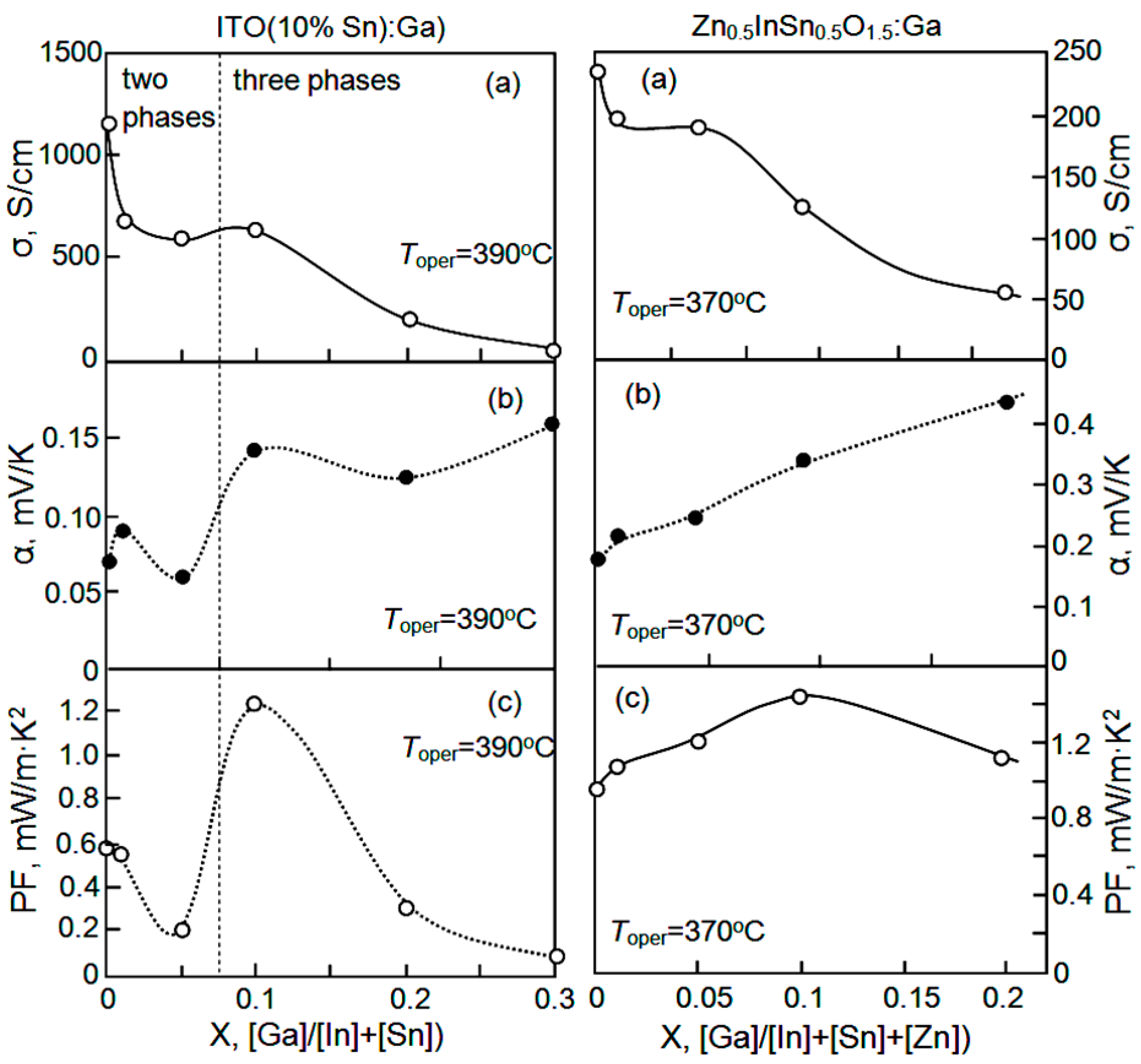
4. In2O3 and Its Advantages for Thermoelectric Applications

When considering the thermoelectric properties of In2O3-based materials, we distinguish three aspects: (1) the electrophysical properties (concentration and mobility of charge carriers), (2) the thermal conductivity of In2O3-based materials, and (3) directly the efficiency of thermoelectric conversion (Seebeck effect, PF and ZT factor).

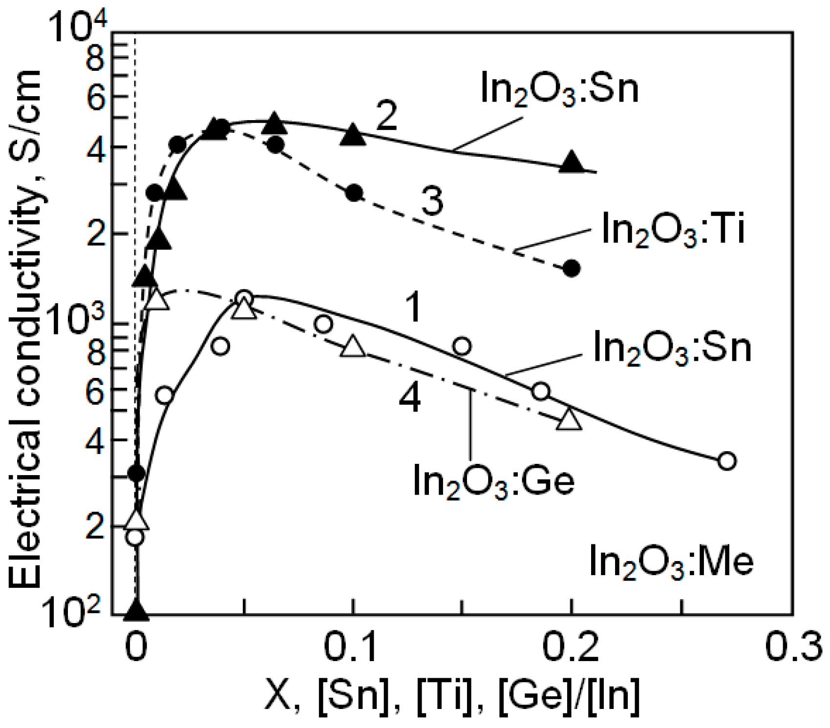
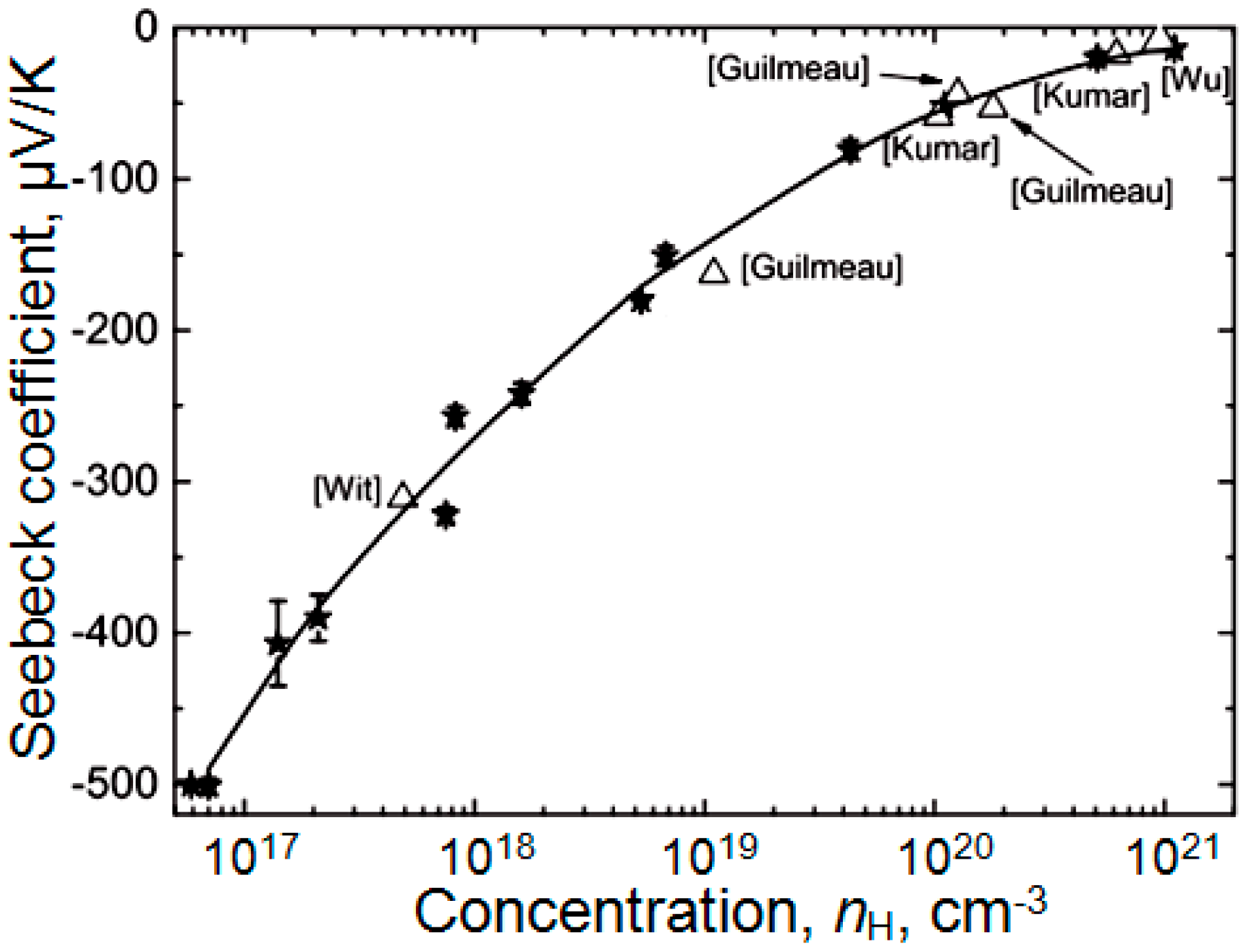
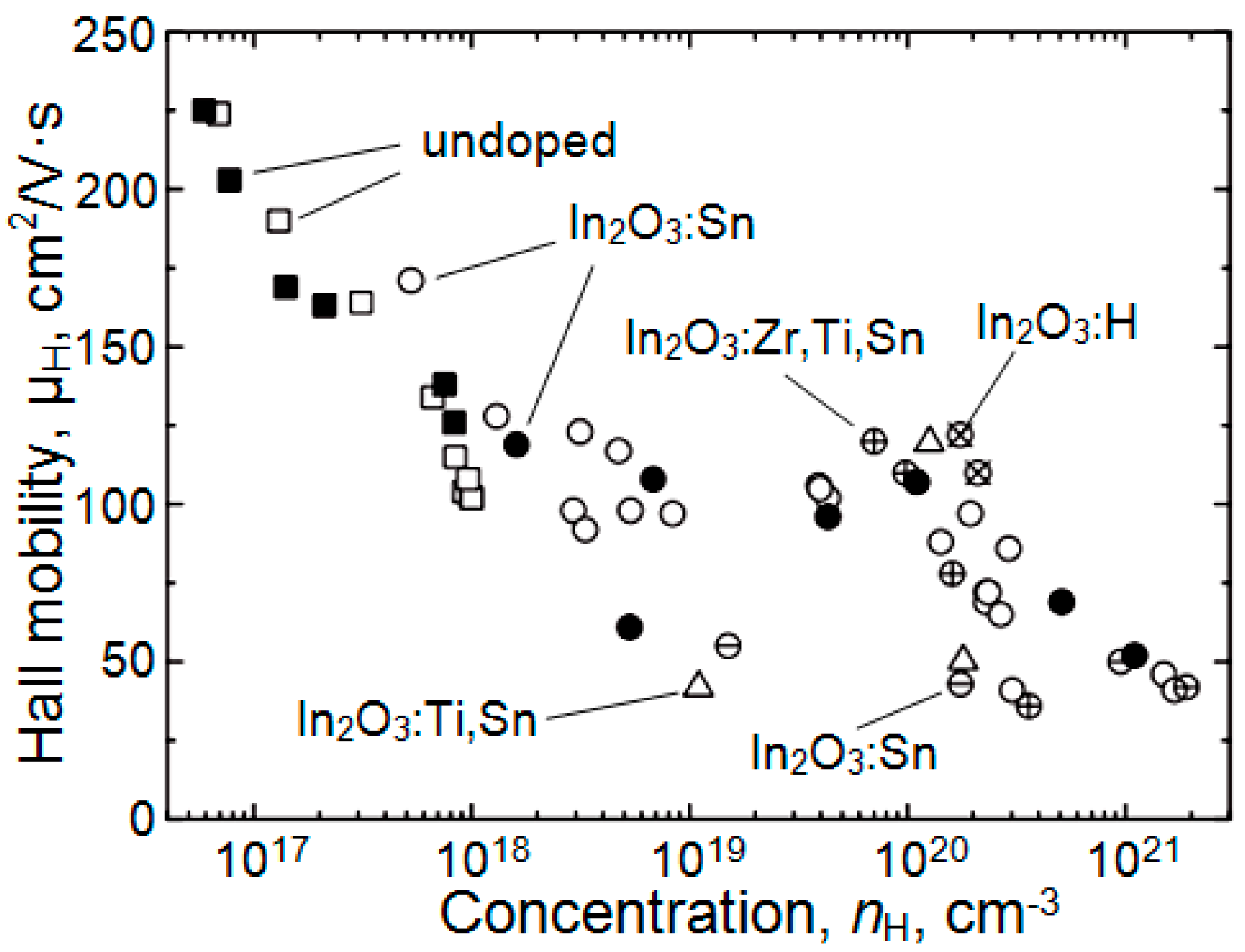
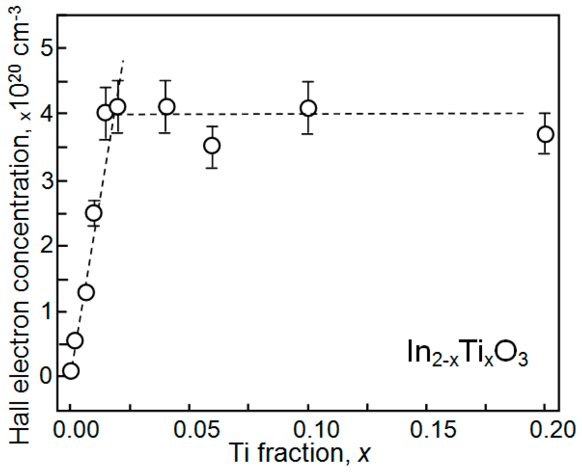
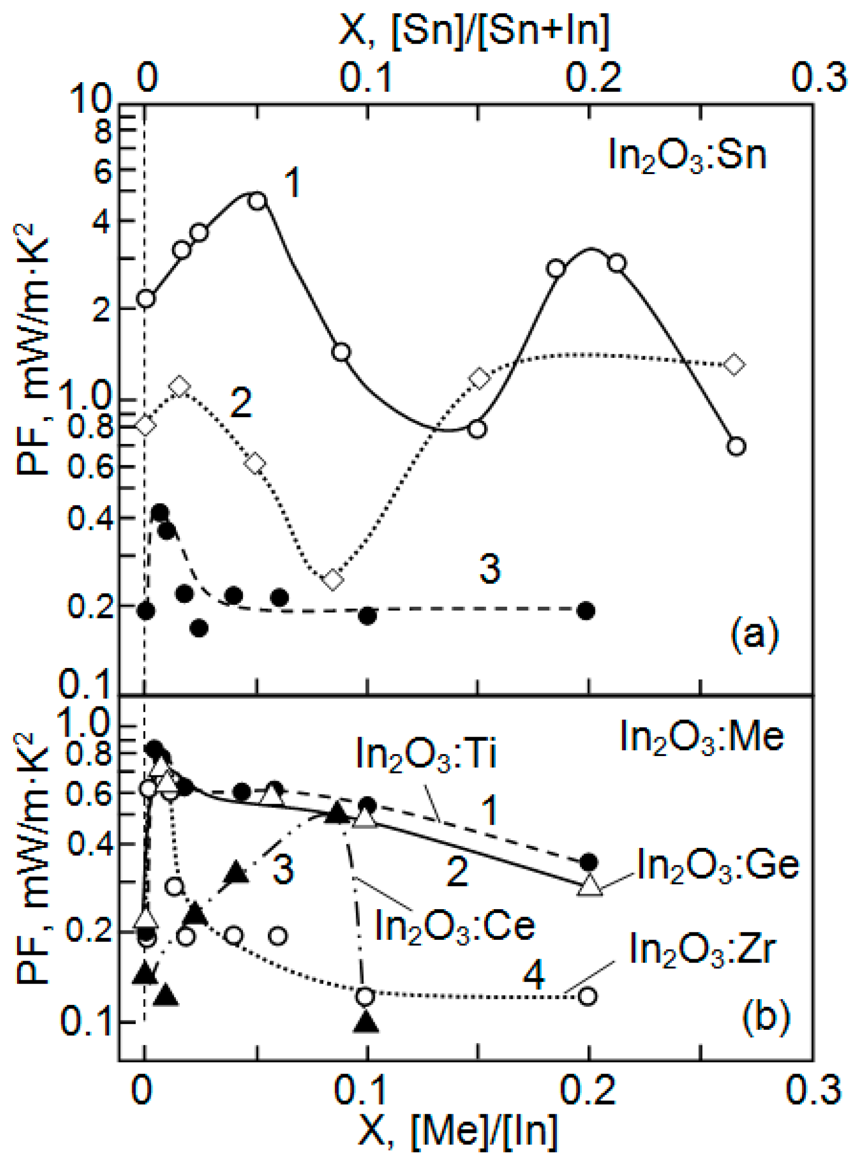
4.1. Electrophysical Properties

As indicated earlier, due to doping, the charge carrier concentration in In2O3 can be increased up to 1020–1021 cm−3. The experiment showed that various doping additives such as Sn [143,144,145], Ti [71], Zr [146,147], Mo [148], W [149] and Ge [70] can be used for these purposes. It is important to note here that with such doping it is possible to reach an exceptionally high carrier mobility in In2O3-based oxides even with a carrier concentration higher than 1020 cm−3 (see Table 1). Of course, owing to its ionic nature, conductive metal oxides like indium tin oxide (ITO) tend to have a carrier mobility that is an order of magnitude lower than Si and other covalent compounds [21]. However, in comparison with other metal oxides, the carrier mobility of In2O3 is indeed high [150]. The experiment showed that even heavy doped n-In2O3 with a resistivity less than 10−4 Ω·cm could have an electron mobility greater than 60 cm2/V·s. For example, Koida et al. [151] reported that a mobility of μ ~ 145 cm2/V·s for N > 1020 cm−3 was observed in ITO after post-deposition treatment in a hydrogen plasma.
The evolution of the electrical conductivity of In2O3 at room temperature versus the Ti, Sn, doping level x is shown in Figure 9. It can be seen that the electrical conductivity increases abruptly for very low x values. Importantly, beyond a certain limit value x, the increase suddenly stops and the conductivity tends to decrease with x. At this point, the concentration of charge carriers remains practically unchanged (Figure 10). It was assumed that beyond x, the substitution of In in the lattice by Ti or Sn no longer takes place, leading to the formation of a secondary phase contributing to the enhancement of charge carrier scattering at additional interfaces, and a decrease in their mobility. This statement was strongly supported by X-ray analysis, which confirms in all cases the appearance of a secondary phase for x > x. In particular, in the case of In2-xTixO3 for x ≤ 0.02, no impurity can be detected, while at x > 0.04 the appearance of In2TiO5 was observed. For all the other In2O3 series with M = Ge4+, Zr4+, Sn4+, Ta5+, and Nb5+, impurity phases such as In2Ge2O7, ZrO2, In4Sn3O12, InTaO4, and InNbO4 are observed when the doping level exceeds the solubility limit, and the solubility limit well matches the ones determined using the transport properties. The limiting solubility for some doping additives are given in Table 2. It can be seen that the limiting solubility of the main additives does not exceed several %. The same situation is observed for other oxides such as ZnO and SnO2 [153]. In the case of In2O3:Sn (ITO), the maximum conductivity is observed at the Sn/In composition ratio of ~5–10% [144]. It should be noted that the most noticeable changes in the thermoelectric characteristics of doped In2O3 are also observed near the dopant concentrations corresponding to the limiting solubility in In2O3 [71,132,136,137].

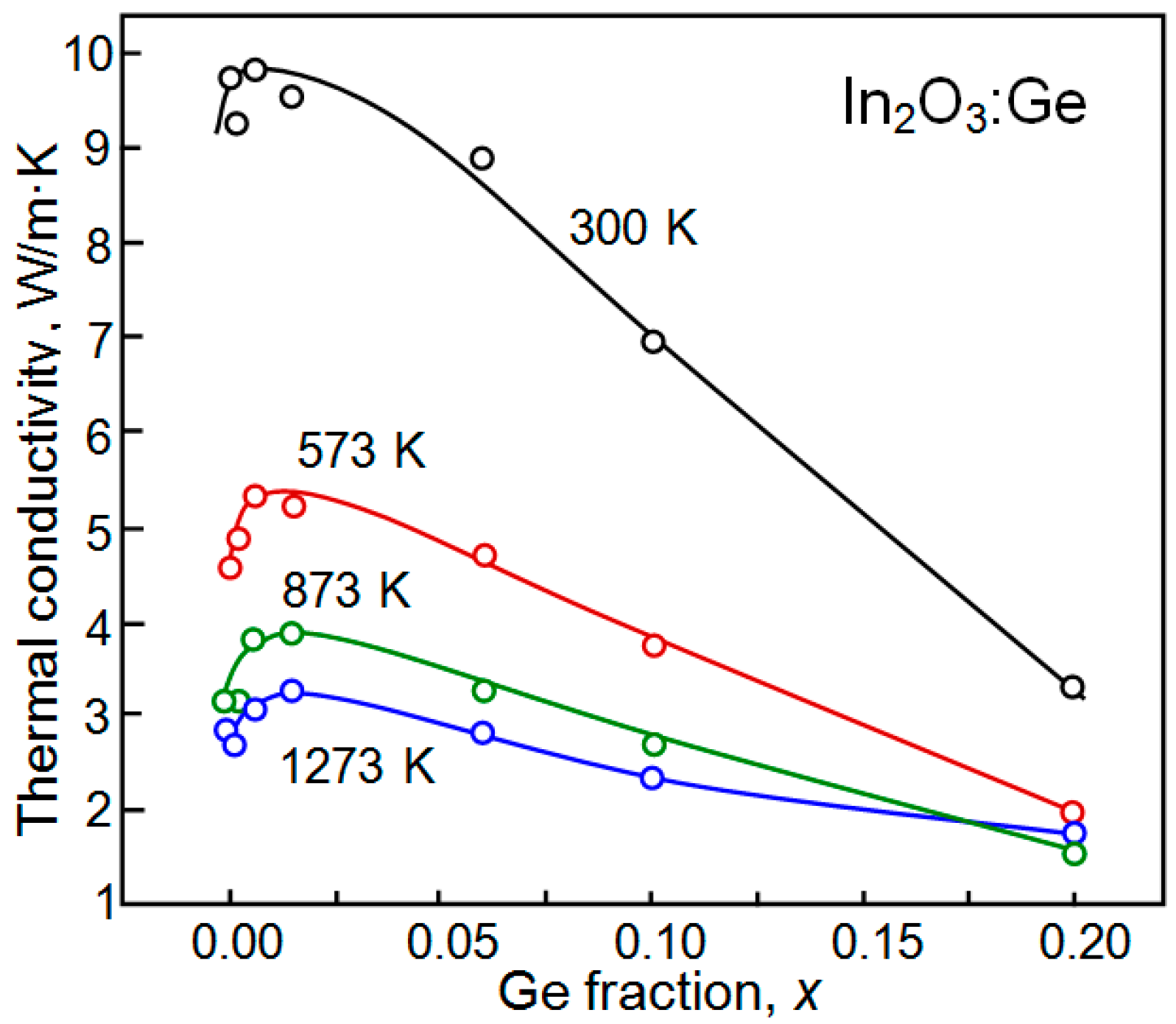
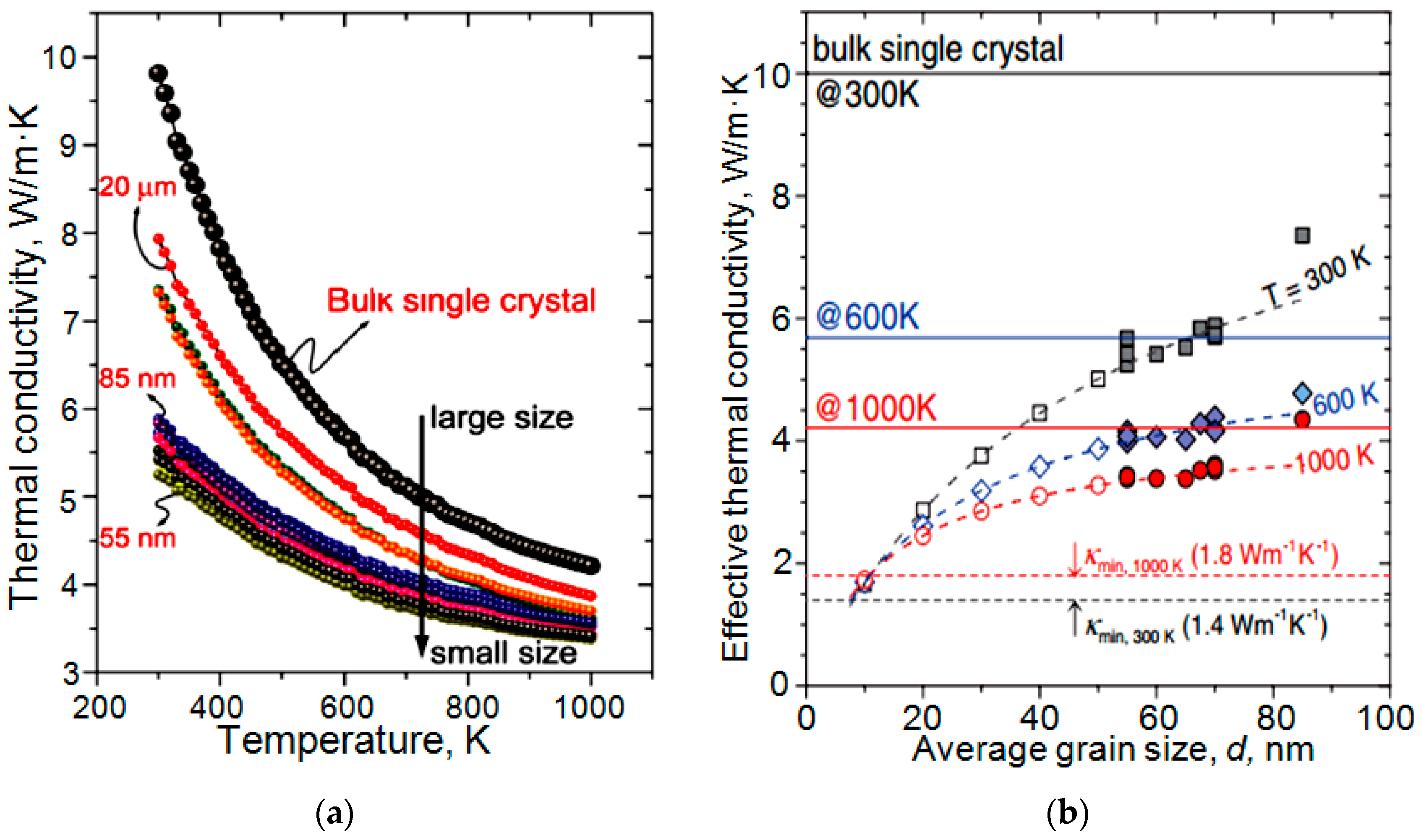
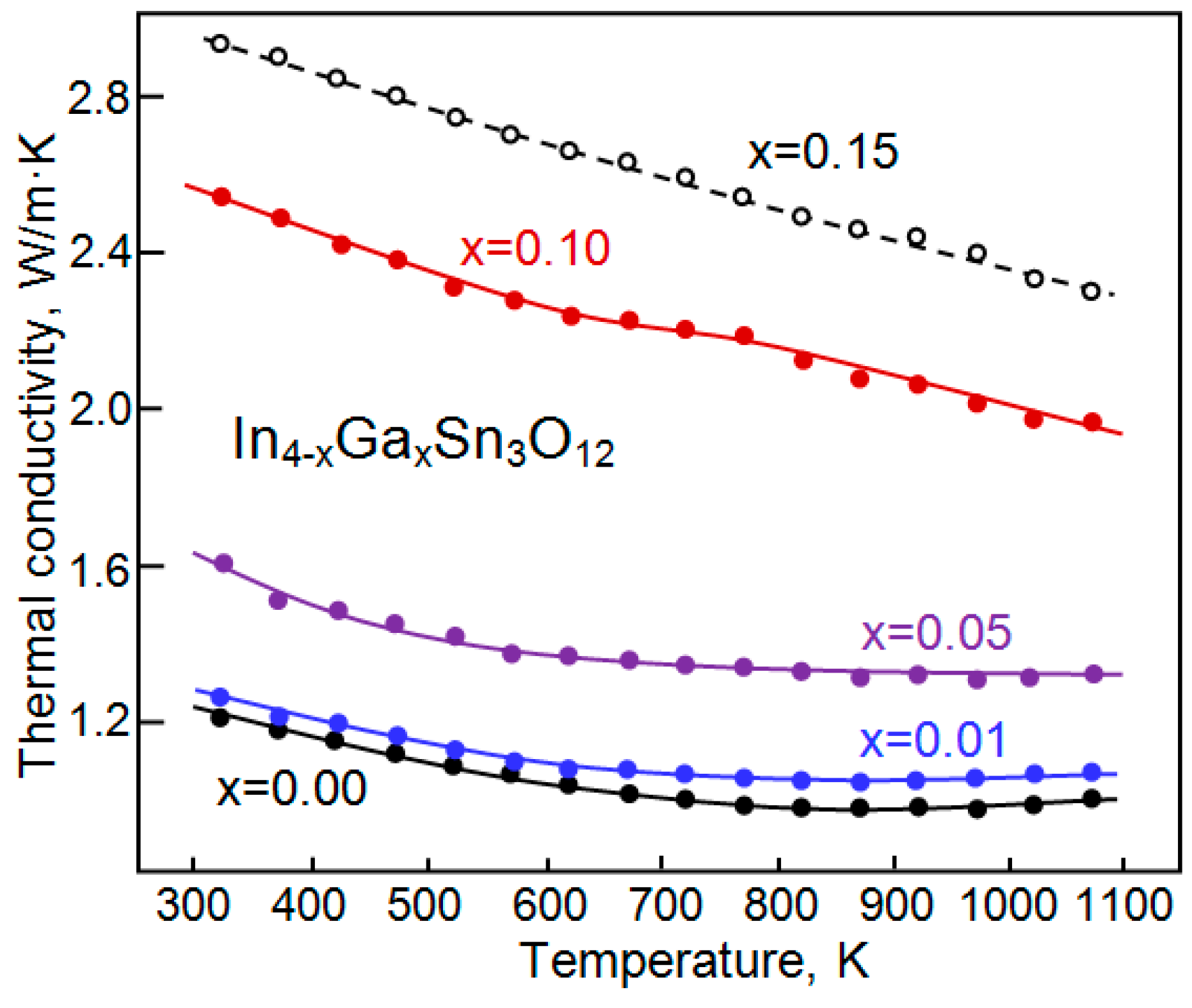
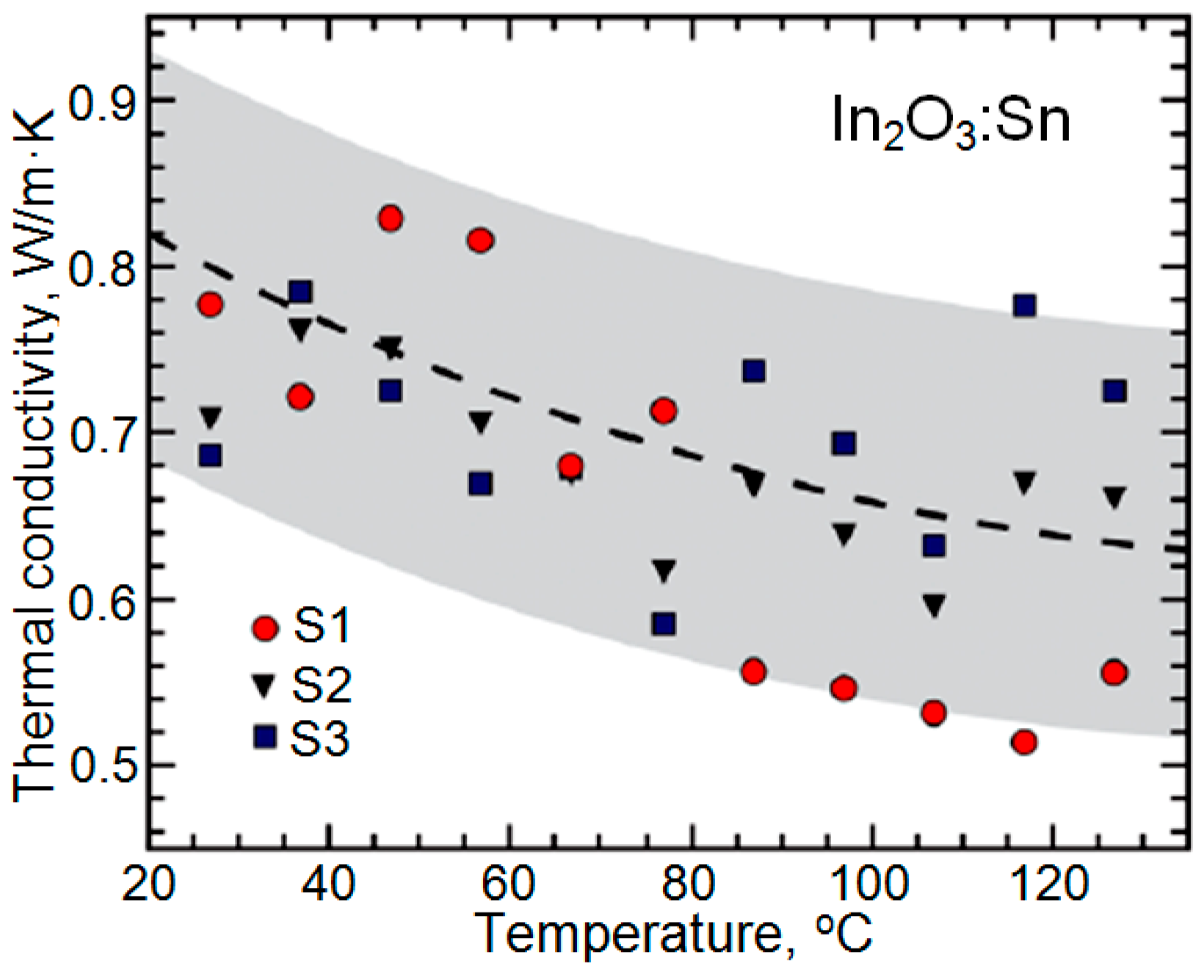
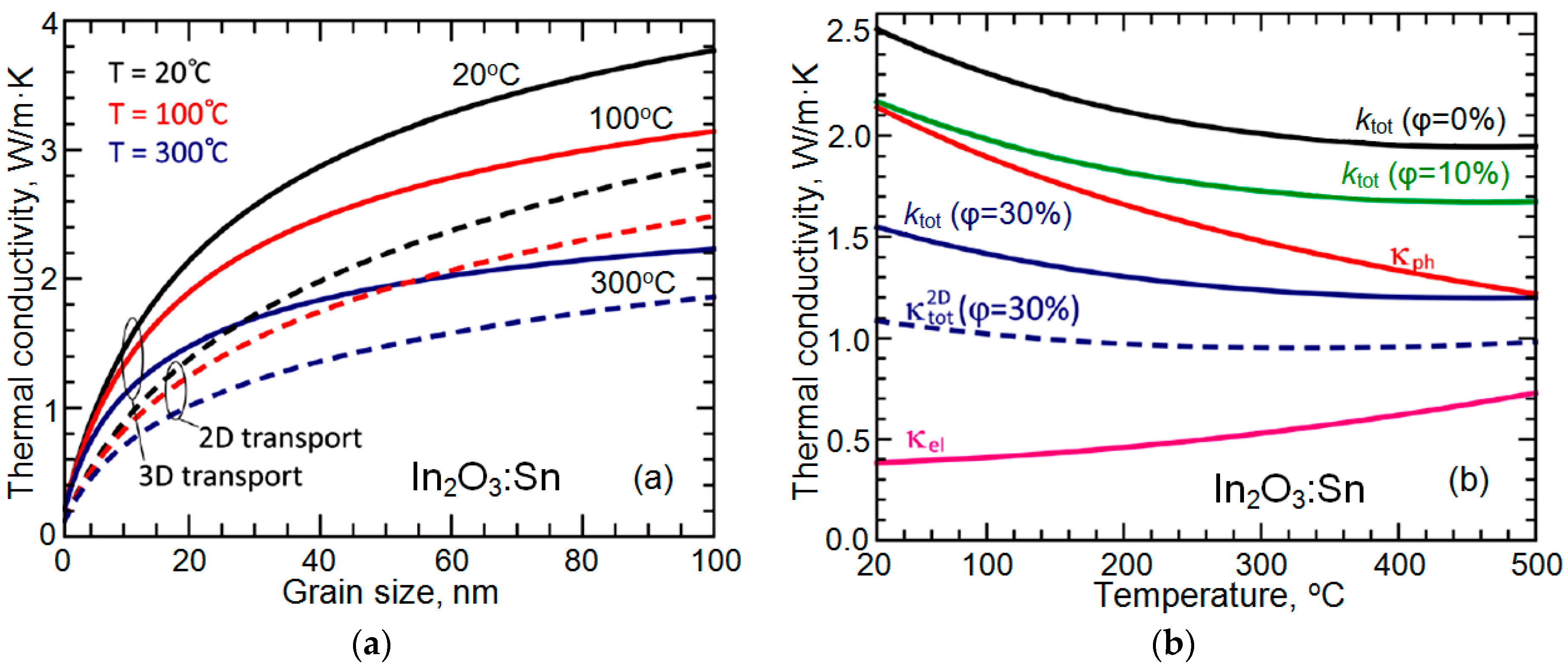
4.2. Thermal Conductivity

It is known that the large bonding energies of the ionic bonds and the small atomic mass of oxygen result in a high velocity of phonon waves propagating through the crystal lattice of the oxide compound. Therefore, bulk-like ITO with tightly-packed large grains (~5 μm) possesses a relatively high total thermal conductivity k ~ 10 W/m·K at room temperature (RT) [70,166], which limits the achievement of the required efficiency of thermoelectric conversion. Therefore, the problem of reducing the thermal conductivity of In2O3-based oxides is an important task in terms of using these oxides as thermoelectric materials.
When using single crystals and sintered samples, this problem is usually solved by the incorporation of dopants, the use of nanocomposites and the altering of stoichiometry [14,33,71,167,168,169]. In particular, randomly-distributed defects and clustered vacancies could provide effective strong short-wavelength phonon scattering, and result in large thermal conductivity suppression, especially at high temperatures [170,171]. Such manipulations change the vibrational properties of the crystal and influence kphonon [17] or by introducing additional scattering sites for phonons, thereby limiting kphonon [44]. This approach is cost-effective and more easily scalable in comparison with the expensive 2DEG (two-dimensional electron gas) and superlattice systems used to reduce thermal conductivity [172]. Important advantages of these approaches include (i) more simple fabrication using a bulk synthesis procedure, compatible with the fabrication technology of existing commercial TE device fabrication, (ii) better mechanical properties, and (iii) a more isotropic structure of the synthesized materials. For example, extra defects such as atomic substitution or oxygen vacancies can be introduced during growth processes in an oxygen-deficient environment [33]. However, one should take into account that kelectron is also affected by changing the stoichiometry and doping level of the TE TMOs. kelectron depends on the electrical conductivity of TMOs (Equation (5)) and is also a function of the Fermi level and charge carrier concentration, which are directly affected by changes of stoichiometry or the incorporation of dopants [173].
As a result of studies carried out in this direction, it has been established that the doping is a less effective method in comparison with the use of composites and complex compounds. In particular, the experiment has shown that the In4Sn3O12 compound, and In4−xGaxSn3O12 and Ga3−xIn5+xSn2O16 phases have a rather low thermal conductivity, as compared to doped In2O3 [143,174,175]. For example, Bhame et al. [143] have reported that the measured thermal conductivity of Ga3−xIn5+xSn2O16 varied from 1.36 to 1.91 W/m·K. The thermal conductivity for the In4Sn3O12 and In4xGaxSn3O12 phase measured by Zhou et al. [174] is shown in Figure 11. This is significantly lower than those reported for other indium-based oxides with optimized thermoelectric properties. For instance, the thermal conductivity of the doped In2O3 compounds was found to be higher than 3 W/m·K [71]. It was assumed that such a situation occurs due to the structural changes in the In2O3 lattice. It is speculated [143] that the complex structure associated with highly disordered Ga3+, In3+ and Sn4+ cations and also the large mass difference between Ga3+ and In3+/Sn4+ are possible reasons for the enhanced phonon scattering.
However, such a large thermal conductivity of doped In2O3 as 3 W/m·K is characteristic of single-crystal or sintered In2O3 [176]. For nanostructured In2O3, the thermal conductivity is much lower. This corresponds to modern views on the nature of this phenomenon and the mechanisms of electron and phonon scattering, responsible for heat transfer [77,78]. The thermal conductivity in nanostructured oxides can be reduced more than the electrical conductivity due to their different scattering lengths [32]. If the unit cell axis of the oxide is smaller than the mean free path of phonons and larger than the mean free path of electrons or holes, it is possible to reduce kphonon by boundary scattering, without affecting σ, which is very important for effective thermoelectric conversion. Doping normally affects short wavelength acoustic phonons. However, mid- to long-wavelength phonons remain largely unaffected and conduct heat in a heavily doped system. In contrast, a nanostructured system can scatter mid- and long-wavelength phonons and thereby further reduce the lattice thermal conductivity. Thus, the decrease in the thermoconductivity of nanostructured materials is due to the reinforcement of phonon scattering on grains and nanoinclusions, leading to a glass-like thermal conductivity [176]. In accordance with these ideas, a decrease in grain size should be accompanied by a decrease in thermal conductivity, which is confirmed by the experiment. For In1.92(ZnCe)0.08O3 this regularity is shown in Figure 8. The rapid decrease of thermal conductivity in comparison with bulk values takes place with the reduction of grain size [38,166,177]. For example, Ohtaki and co-workers. [28,178] demonstrated that in nanostructured In2O3:MOx (M = Cr, Mn, Ni, Zn, Sn) ceramics, the thermal conductivity decreased to k ~ 1.58–1.75 W/m·K at RT irrespective of the chemical nature of the second phase. Lan et al. [166] reported on the thermal conductivity k ~ 1.2 W/m·K at 973 K in sintered In2O3 doped by Zn and Ce that is below the amorphous limit [142]. Approximately in the same range was the minimum thermal conductivity of In2O3 doped with Ge [70]. The effect of doping additives on the thermal conductivity of In2O3:Ge is shown in Figure 12.
In compliance with Ohtaki [178] and Ren et al. [33], a decrease in the thermal conductivity should also be facilitated by an increase in the porosity of the samples to a certain limit. For example, the best thermoelectric characteristics in the experiments carried out by Ohtaki [178] were observed for the samples of In2O3:MOx, with a relative density around 65–70%. The thermal conductivity in porous materials is decreased because the phonon is scattered by an ordered pore structure. However, one should know that if the spacing between the nanoparticles is larger than the electron mean free path (MFP), they will act as an additional source of electron scattering in the host material [179].
Brinzari et al. [134] have demonstrated that due to the enhancement of phonon scattering on grain boundaries in nanogranular ITO films, the thermal conductivity can be reduced even more. They have shown that in thin films (d ~ 90–300 nm) with a grain size ~20 nm, the thermal conductivity can have ultra-low values ~0.84 ± 0.12 W/m·K at room temperature (see Figure 13). It can be seen that the thermal conductivity weakly decreases with a temperature rise up to 140 °C. The obtained values of RT kITO are approximately one order of magnitude lower than that of bulk ITO [70,166] and by a factor of 2–5 lower than that of ITO thin films prepared by other techniques [28,177,178].
The variation in thermal conductivity values in Figure 12 is explained by the different porosity and dispersion of grain sizes in S-1, S-2, and S-3 samples, resulting in different strengths of phonon scattering on the grains. Li et al. [65] have reported that a large dispersion of grain size in nanostructured films and the inevitable appearance of porosity should lead to the enhancement of phonon scattering and a reduction of thermal conductivity.
To understand this behavior of the thermoconductivity of nanogranulated In2O3 films, Brinzari et al. [134] conducted a simulation of electron and phonon transport in these films. The results of these simulations for different temperatures are shown in Figure 14. It can be seen that the thermal conductivity dropped by a factor of ~2 with a decrease in the grain size from 100 nm to 20 nm. The temperature dependence of phonon, electron, and total thermal conductivity is presented in Figure 14b by red, magenta, and black curves, correspondingly. The phonon thermal conductivities are plotted for the grain size lG ~ 20 nm, which is typical for the ITO films used in experiments conducted by Brinzari et al. [134]. The phonon thermal conductivity decreases with temperature due to an enhancement of phonon–phonon scattering, while electronic thermal conductivity demonstrates an opposite trend. The non-linear growth of kel is explained by an increase in the total number of electrons participating in electronic transport over the barrier with temperature rise.
The calculated RT total thermal conductivity k = 2.5 W/m·K is larger than the average experimental value. Brinzari et al. [134] believe that this discrepancy may be attributed to two reasons: (i) the porosity of ITO films and (ii) anisotropy in the grain size, shape, and alignment. Using effective medium approximation [180,181], the effect of the porosity was estimated; it was found that 30% porosity decreases the thermal conductivity by 39% for 3D phonons and by 57% for 2D ones. The obtained RT 2D thermal conductivity k2Dph ~ 1.1 W/m·K is in reasonable agreement with the experimental value kITO ~ 0.84 ± 0.12 W/m·K. Slightly lower values of experimental kITO can be attributed to irregularity and scattering in the size, shape, and orientation of grains, resulting in the possible trapping of phonon modes in grain segments. This effect is similar to phonon mode trapping in segmented and cross-section modulated nanowires, leading to a drastic reduction of phonon thermal conductivity [182,183,184,185].

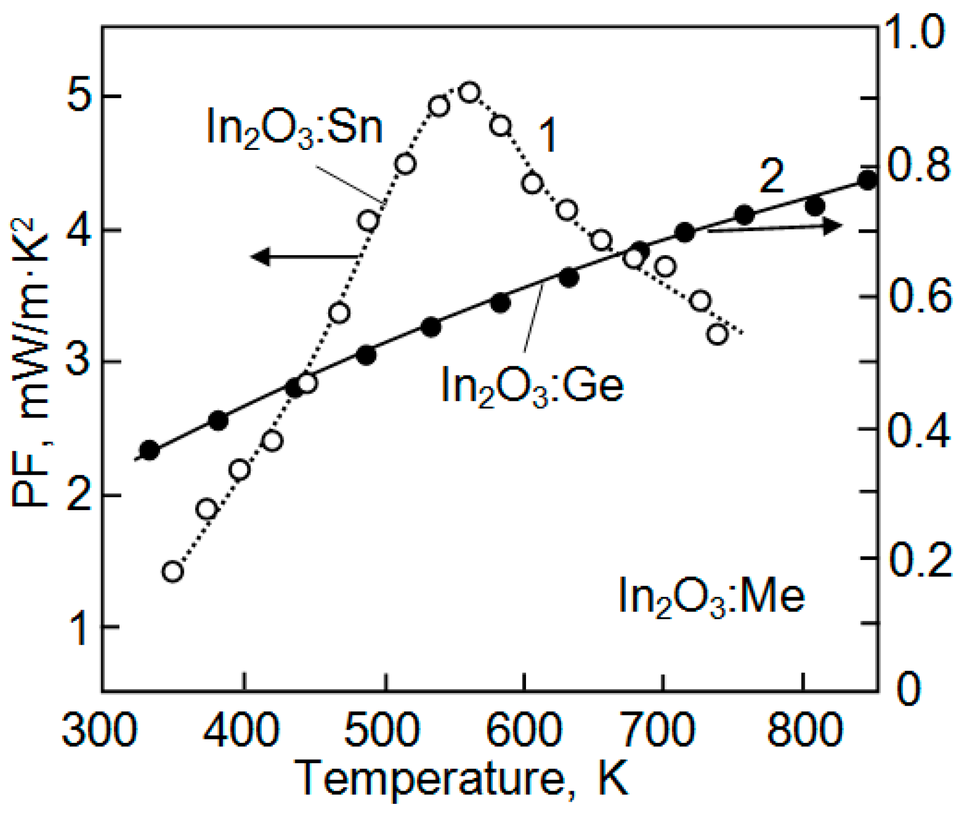
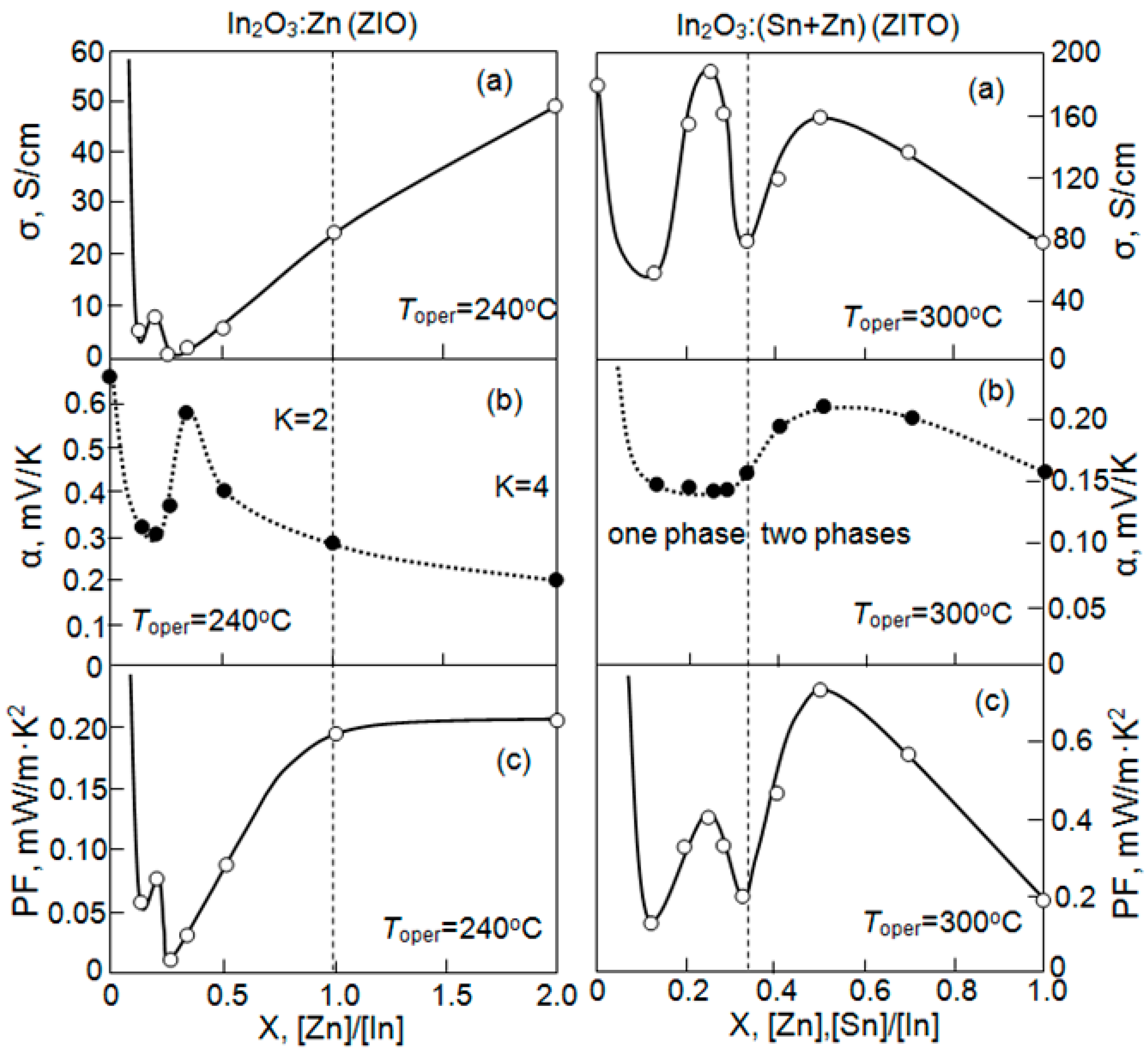
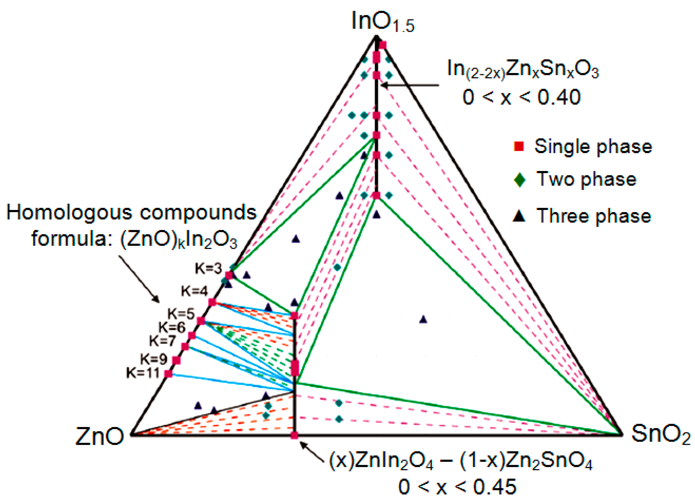
4.3. Thermoelectric Conversion Efficiency of In2O3-Based Oxides

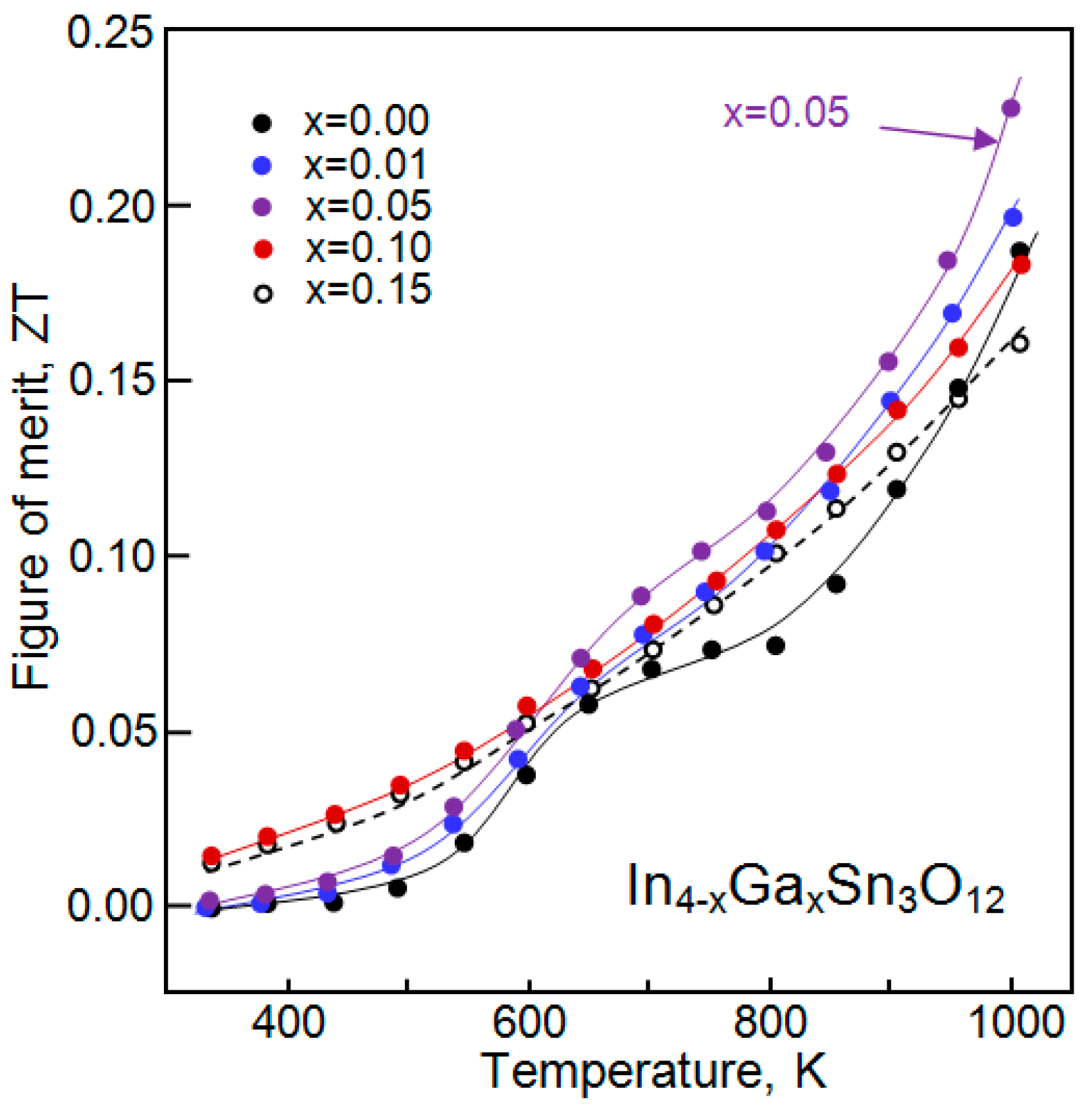
4.3.1. Sintered Samples

Earlier in the study of thermoelectric properties, the main emphasis was paid to In2O3-based materials subjected to high temperature sintering with the purpose of increasing the density and reducing the porosity [31,38,70,71,113,114,185,186,187,188,189]. For example, the In2O3(ZnO)3 samples studied in [120] were sintered at 1300 °C. The effect of annealing on the In2O3 and ITO densities is shown in Figure 15. As a result of these studies, it was found that doped In2O3-based fluorite derivative structures showed fairly good thermoelectric performance. Some of the most significant results of these studies are summarized in Table 3. As can be seen from the Table, these results refer mainly to In2O3 doped with Ge [70], Ga [40], Ce [39,188], Ti [29], Zn [115], and Sn [71,145].
The results obtained for the In2O3:Ti system are shown in Figure 16. As a representative trend for the different studied cationic substitutions, minima values of ρ and |S| around their solubility limit were observed (x = 0.02 for Ti-doped system). According to the Seebeck and electrical resistivity values, the highest value of the power factor, ~0.9 mW/m·K2, was reached for intermediate doping levels, i.e., below the solubility limit. At these doping levels, high mobility, and moderate carrier concentrations associated with high thermopower give the best electrical performances [71]. The doping fraction dependence of the thermal conductivity follows the same behavior as the electrical conductivity. The highest values of k are found around the solubility limits. As expected, the increase in the thermal conductivity (mainly the electronic contribution) is correlated with a decrease in the electrical resistivity. Further additions of dopant above their solubility limits lead to a slow decrease in the thermal conductivity due to the slow increase in the electrical resistivity.
In principle, a similar situation is observed for all doped In2O3-based materials [29,39,40,70,71,115,145,188]. As a rule, the highest ZT values for all the series were reached for the low doping levels where high-power factors were combined with low thermal conductivities. However, despite the growth of the thermopower and conductivity in doped, sintered In2O3, regardless of the dopant used, the ZT did not exceed ~0.3 at 1000 K (see Table 3).
Similar patterns were also observed for more complex sintered In2O3-based compounds, which have been studied with the aim of reducing the indium concentration in thermoelectric materials. As was indicated before, indium is a quite expensive element. Pitschke et al. [196], studying In4Sn3O12, concluded that this system is a poor thermoelectric material with a ZT ~ 0.03 (1000 K), while Zhou et al. [174] have established that this material after the addition of small amounts of Ga2O3 and reactive sintering had a ZT ~ 0.25 at the same temperature. This maximum originates from the combination of significantly low electrical resistivity and thermal conductivity as compared to the parent In4Sn3O12 composition. It is important to note that, as in the case of doped In2O3, the maximum ZT value at 1000 K for In4−xGaxSn3O12 was obtained at a very small x = 0.05.
A ZT not exceeding 0.3 also had oxides from In4−xGaxSn3O12 [174] and Ga3−xIn5+xSn2O16 [143] systems. The results of In4−xGaxSn3O12 testing are presented in Figure 17. It was shown that like the doped In2O3 phase, these complex oxides are an excellent TCO [197] and good thermoelectric materials [143,174]. For example, the testing of Ga3−xIn5+xSn2O16 phase with a rather high room temperature conductivity of 375 S/cm [143] has shown that the maximum value of the Seebeck coefficient, 145 μV/K, was observed for x = 0.3 at 1000 K, while the maximum power factor value of 0.55 mW/m·K2 was observed for x = 1.6 at 1000 K, as compared to the value of 0.36 mW/m·K2 for x = 0.3. It should be noted that these values are slightly lower than those observed in the Ge-doped In2O3 [70]. The influence of the Ge concentration in In2O3 on ZT is shown in Figure 18. It can be seen that ZT did not exceed 0.4 at 1273 K. These values were due to the fact that the Seebeck coefficient did not exceed 240 μV/K even at 1000 K, and the thermal conductivity did not fall below 1.5 W/m·K [70].

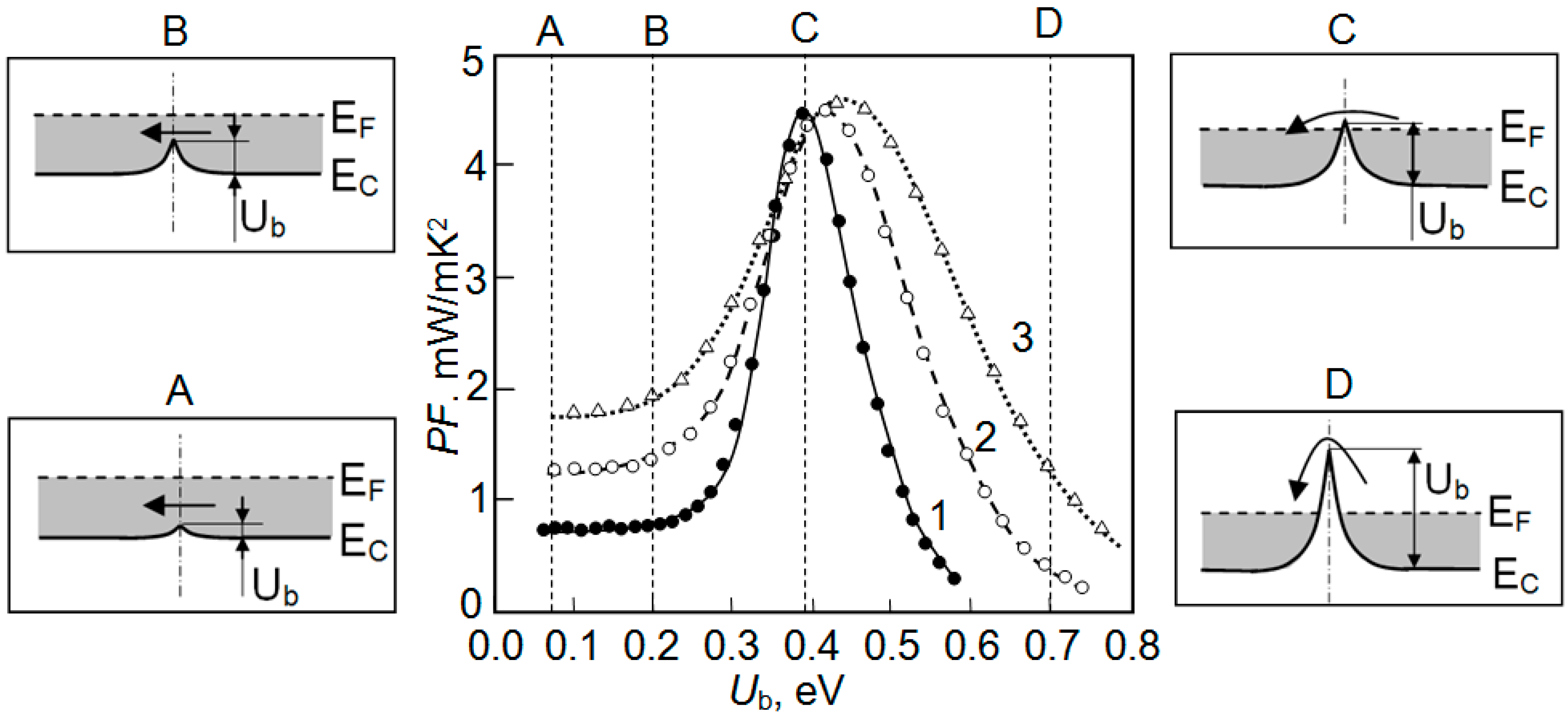
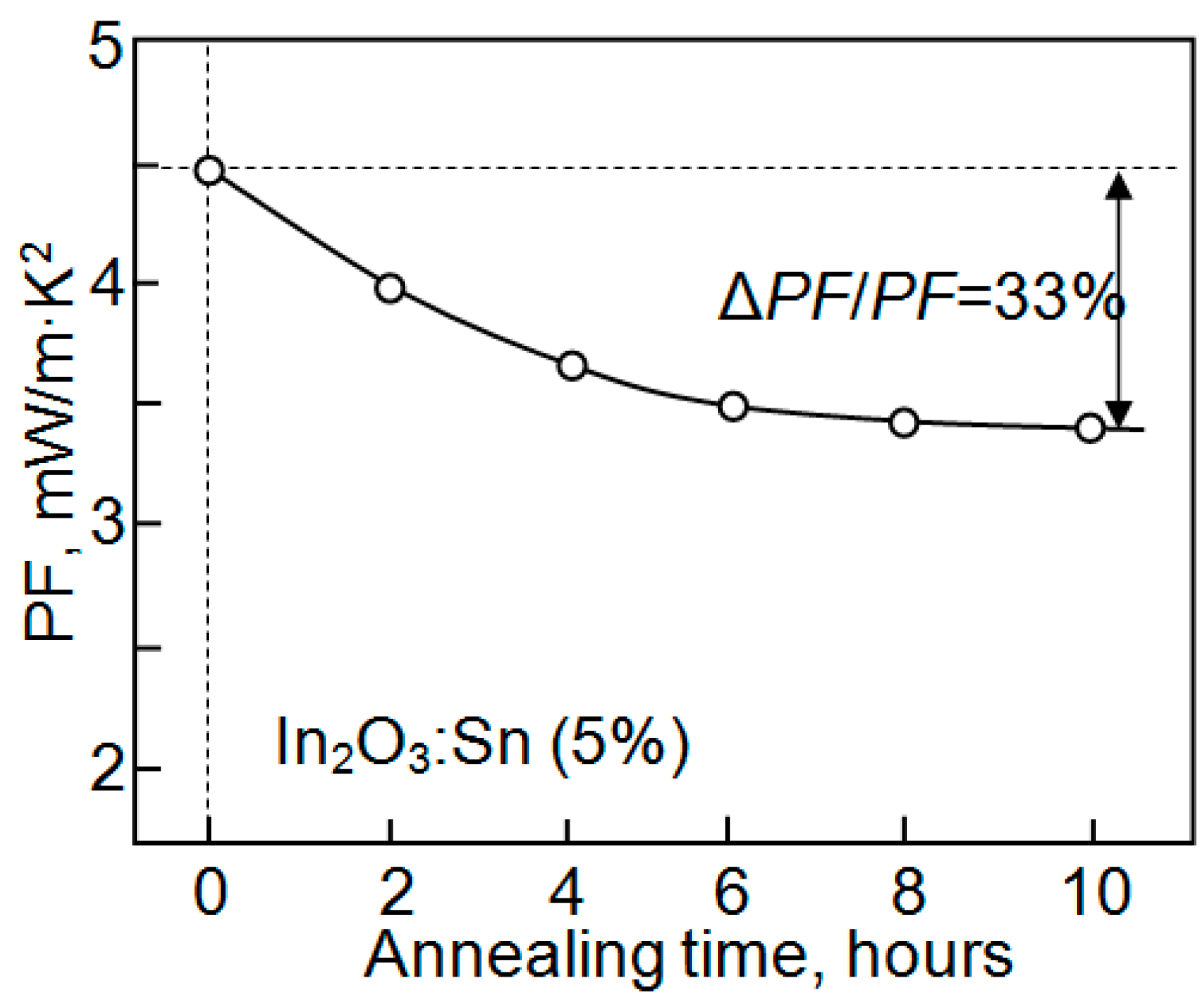
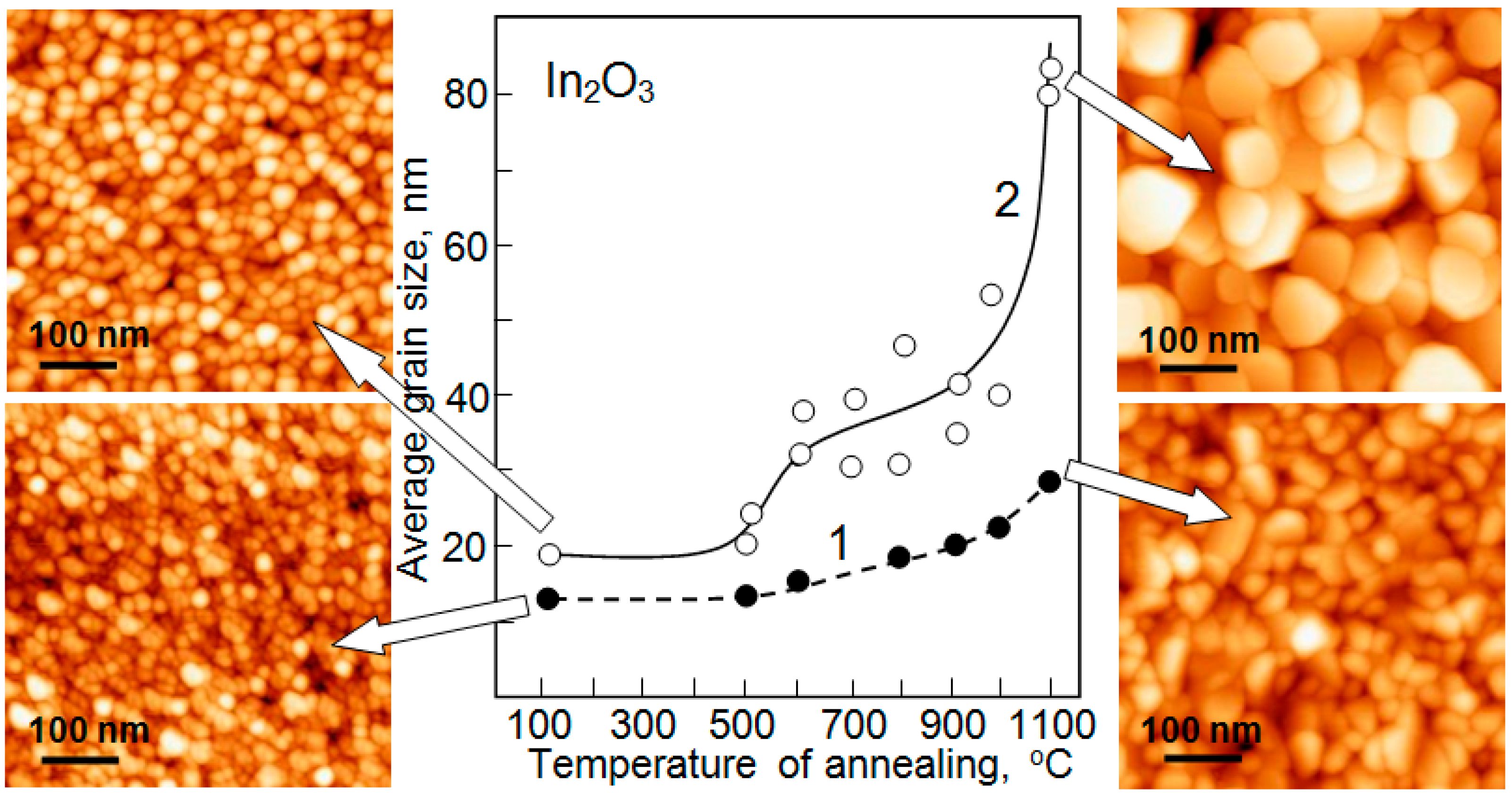
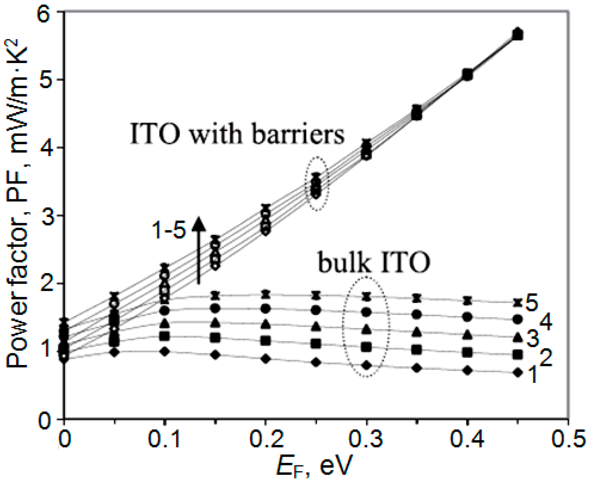
4.3.2. Thin Nanostructured In2O3 Films

As can be seen from the above discussion, the usage of sintered In2O3 samples did not provide any appreciable improvement of thermoelectric converter performance in comparison with SrTiO3 or ZnO. In most cases, the Seebeck coefficient, PF and ZT had values typical for these n-type metal oxides. At the same time, studies performed using thin-film nanostructured In2O3 doped with tin showed that, in this case, a significant improvement in the parameters of thermoelectric converters can be achieved. According to Brinzari et al. [132,133,134] and Korotcenkov et al. [135,136,137], In2O3:Sn is among the most promising n-type metal oxides for thermoelectric applications. Doping with tin, which is a donor to In2O3, provides necessary increase in the conductivity of the films. In particular, studies carried out by Brinzari and Korotcenkov showed that nanostructured In2O3:Sn films (d ~ 90 nm) with a grain size of 25–30 nm had a much higher efficiency of thermoelectric conversion (Figure 19a) in comparison with In2O3 prepared using a conventional approach based on synthesis and high temperature sintering. If the best In2O3:Sn samples, densified during high-temperature annealing at T = 1000–1500 °C, with a crystallite size of tens of micrometers, had a power factor of 0.4–0.5 mW/m·K2 [39,70,71], then nanoscaled In2O3:Sn films had a PF reaching 4–5 mW/m·K2. At the moment, this is the best result obtained for the n-type metal oxides designed for thermoelectric applications (Figure 19b). This demonstrates that nanoscale metal oxides are promising materials for thermoelectric convertors, because the observed increases in the efficiency of converting heat into electricity make the use of thermoelectric generators cost-effective. For example, using PF ~ 3 mW/(m·K2) at T = 300 °C, as reported in [136], and the value of measured kITO ~ 0.9 W/m·K [134], one can roughly estimate a ZT ~ 1.9 for optimally-doped nanostructured ITO films.
The analysis of the In2O3:Sn films properties showed that such values of PF cannot be explained by specific electrophysical parameters of the films studied, since the electrical conductivity of the In2O3:Sn films did not exceed the value usually observed for In2O3-doped with different impurities (Figure 9). A more detailed examination of the reasons for this behavior of the thermoelectric properties of the In2O3:Sn films led to the conclusion that the increase in the efficiency of thermoelectric conversion occurred due to the nanoscaled structure of the films studied. The research results reported by Vashaee and Shakouri [75] and Koumoto et al. [14] and calculations for In2O3:Sn with optimal doping carried out by Brinzari et al. [133] showed that a so-called filtering effect was possible in such nanoscaled structures and at a certain ratio of the Fermi level and band bending, Ub, this effect could create a rise in power factor of more than five times. Figure 20 illustrates the procedure of electron filtering by potential barriers. According to this model, electrons with energies higher than the barrier height (UbEF) can participate in electron transport. Figure 21 shows the results of a conducted simulation. They indicate that the increase in the PF due to the filtering effect can be achieved in semiconductors of n-type conductivity if the band bends upwards and the height of the potential barrier, UbEF, exceeds only by a few kT the position of the Fermi level in the conduction band. Band diagrams showing the change in the current transport mechanism on changing Ub are shown in the same Figure 20.
From our point of view, such a strong influence of the filtering effect on the thermoelectric properties of In2O3 is a consequence of the combination of the specific surface properties of In2O3 [198,199], the successful choice of type and concentration of the dopant [132], and the appropriate structural properties of the films. As mentioned previously, the maximum filtering effect is achieved when the band bending, Ub, at the grain boundary is only a few kT greater than the energetic position of the Fermi level, EF, in the conduction zone. This means that the Ub should be small. Studies of the surface and electrophysical properties have shown that this is the situation that is realized in In2O3. If in most n-type oxides, such as SnO2 or ZnO, the height of the potential barrier at the grain boundary in the oxygen atmosphere can exceed 0.5–0.8 eV [199], then for In2O3 under these conditions a flat-band situation can be realized. This situation is shown in Figure 22. Therefore, only a small correction of the surface properties is required to achieve the maximum influence of the filtering effect. Doping with tin seems to fulfill this role. We believe that the observed correction of the surface properties of the In2O3:Sn grains is the result of the combined action of the following three factors. The first one is the change in electronic states of indium oxide under the influence of doping with tin [200], the second one is the segregation of the tin atoms in the surface layer, which is accompanied by the accumulation of charged defects in the structurally-distorted surface region, and the last one is oxygen chemisorption on the surface of the In2O3:Sn grains which is accompanied by the capture of electrons from the conduction band. It should be noted that the influence of metal oxide doping on the height of the potential barrier at the inter-crystallite boundary was experimentally confirmed in the studies carried out in [201,202].
With regard to the structural properties, according to the estimations conducted in [133], the filtering effect starts affecting the thermoelectric properties when the crystallite size becomes smaller than 50–70 nm, and this influence increases with the decrease in the grain size. As indicated in [132], the crystallites in films, showing high values of the power factor, had a size lying in the range of 10–40 nm. For comparison, in sintered In2O3 samples, the crystallite size exceeded 100 nm. The important role of the crystallite size in thermoelectric effects is confirmed by the fact that the increase in the pyrolysis temperature up to 450 °C, which was accompanied by an increase in the crystallite size to 40–50 nm, resulted in a decrease in PF to 1.0–1.5 mW/m·K2 (Figure 19a, curve 2). The increase in the power factor with the decrease in grain size was also observed by Lan et al. [38]. The grain size decrease from 600 to 50 nm in the In1.92(ZnCe)0.08O3 samples was accompanied by an increase in PF from 0.45 to 0.8 mW/m·K2. Importantly, the reduction in the grain size also helped to reduce the thermal conductivity of In1.92(ZnCe)0.08O3 samples [38], another parameter whose reduction is required to increase the ZT.
In the nanoscaled granulated materials, it is also necessary to take into account the height of the potential barrier at the intergrain interface, which controls the conductivity of the film and filtering effect and depends on the concentration of oxygen and water chemisorbed on the surface of the crystallites. As is known, the concentration of oxygen and water chemisorbed on the metal oxide surface is controlled by the surface processes and is dependent on both temperature and surrounding atmosphere, including air humidity [204,205]. As a result, the power factor of the nanoscaled materials can have fundamentally different temperature dependences compared to sintered materials, where the influence of the surface effects on the value of PF is minimized (Figure 23). Unlike a monotonic increase in the power factor with the increasing temperature observed for the sintered In2O3 films (Figure 23, curve 2) [28,70], for nanoscaled In2O3 films, the appearance of a maximum at T ~ 250 °C is observed in PF = f (T) dependences (Figure 23, curve 1).
This means that when using the nanoscaled materials, there are additional factors which should be controlled. Of course, such a situation complicates the use of devices based on such materials. On the other hand, in this case, we get additional opportunities to influence the efficiency of thermoelectric conversion. In particular, through changes in operating temperature and the surrounding atmosphere, we obtain the possibility to influence the height of the potential barrier between the crystallites and thereby achieve the maximum impact of the filtration effect on the thermoelectric conversion. For example, according to references [204,205], a maximum power factor is observed at a temperature, ~250 °C, which corresponds to the temperatures at which the desorption of water from the surface of In2O3 and a slight decrease in Ub take place. Considering the strong optimizing influence of the filtration effect on the efficiency of thermoelectric conversion (Figure 21), one can suggest that by controlling the surface state of the In2O3 crystallites, the values of PF and ZT, acceptable for practical use, may be achieved at temperatures which are significantly below 1000 °C. This will allow the exploitation of nanoscaled materials in thermoelectric convertors without the threat of the degradation of their parameters, which was observed for nanostructured In2O3:Sn films after prolonged exposure to high temperatures (T ≥ 700 °C) (Figure 24). Analysis of possible reasons for power factor decrease during the long-term thermal annealing of the In2O3:Sn films revealed that these changes could be due to an increase in the crystallite size caused by their coalescence. The effect of annealing on the crystallite size in the In2O3 films is shown in Figure 25. It can be seen that significant changes in the crystallite size are observed after annealing already at T = 500–600 °C. It is important to note that in the nanocrystalline In2O3 pellets from the powder synthesized by the sol–gel method, the process of solid state sintering (densification) starts in the same temperature range [190]. According to Løveng Sunde et al. [190], the grain size in the In2O3 pellets prepared from the synthesized powders increased from 25 to 180 nm, when the annealing temperature increased from 600 to 1000 °C.
There are no doubts that sintered In2O3 samples are characterized by a significantly better stability of structural parameters and that they can therefore operate at substantially higher temperatures without the degradation of their properties. As is known, structural stability depends on the size of the crystallites. The larger the grain size, the higher the temperature at which the transformation of the structural properties of the materials begins [206]. However, in sintered samples, where the crystallite sizes reach several micrometers, wide intergrain necks are formed due to high-temperature treatment, over which a barrier-free transfer of charge carriers occurs. This means that the filtration effect observed in nanostructured In2O3:Sn samples, which creates such a strong optimizing effect, cannot be realized in sintered samples. The graphs presented in Figure 26 show PF dependences as a function of the Fermi level position connected with the electron concentration. They contain two families of curves, which correspond to two cases in the ITO structure: the bulk material and granular ITO with potential relief (barriers). It can be seen that for the bulk (sintered) material we have a maximum PF at some electron concentration (EF ~ 0.1–0.2 eV or no ~ 0.6–1.2 × 1020 cm−3), while for granular ITO the PF increases monotonously with EF reaching significantly higher values. In this regard, it is quite obvious that when working with nanoscaled materials, it will be necessary to make a choice, either to increase the crystallite size with the purpose of improving the stability at high temperatures or to reduce the operating temperature, so that it is possible to use films with a small grain size. Only future study will show which approach is more effective. However, for reasons of achieving the maximum efficiency of thermoelectric conversion, it seems better to work at lower temperatures, but with nanostructured samples. If, due to an increase in the operating temperature from 500 to 1000 K, we can obtain the growth of ZT by a factor of two, then due to the filtration effect we can achieve an increase in ZT in In2O3:Sn samples by a factor of 4–5 (see Figure 21). If we take into account that thermal sources typically have a temperature not exceeding 500–600 °C, then such a choice is quite natural.
Certainly, one can try to improve the high-temperature stability of nanostructured oxides. Generally, an improvement in the structural stability of the metal oxide is solved by introducing a second component into the metal oxide, which is due to segregation at the surface of the crystallites, preventing interaction between crystallites and their coalescence. In principle, the very doping with tin already contributes to some improvement in the stability of the ITO structure (see Figure 15). However, the experiment showed that the introduction of the second component cannot completely prevent the growth of crystallites during high temperature annealing [153]. Doping only reduces the possible structural changes in metal oxides. Furthermore, the range of impurities which may be used in thermoelectric materials is very limited. First, these impurities must be donor or isoelectronic, i.e., electrically inactive. Second, the second metal oxide phase, which is formed during doping by these impurities, must be highly conductive. Third, the oxides formed by these elements must have a high melting temperature and these doping impurities should not form liquid phases due to eutectic reactions. Otherwise, the introduction of these elements will be accompanied by a strong decrease in the conductivity or will stimulate structural changes in the film during the heat treatment. According to the available experimental results, the impurities that are contraindicated for use in thermoelectric In2O3 include Mg, Nb, Y, Mn, Si, Al, Lu and Fe. In addition, the effect of crystallite size stabilization is usually observed at concentrations exceeding the solubility limit of these additives in the main metal oxide. Unfortunately, these concentrations are unacceptable for thermoelectric materials, since at these concentrations there is a decrease in electron mobility and conductivity due to the increase in the concentration of structural defects [207]. As a result, the thermoelectric parameters of the oxides should deteriorate. As shown in the studies performed by Korotcenkov et al. [136,137], this is situation was observed in the study of metal oxides from ZnO–In2O3, (ZnO + SnO2)–In2O3 (Figure 27), Ga2O3-ITO and Ga2O3-Zn0.5InSn0.5O1.5 systems (Figure 28). It can be seen that the electroconductivity and power factor determined for these metal oxides, especially when using oxides from ZnO–In2O3 and (ZnO + SnO2)–In2O3 systems, are significantly smaller than the values observed for ITO (see Figure 27). This means that the hypothetical improvement of ZT due to the possibility of using higher operating temperatures does not compensate for the deterioration caused by introducing an additional component.
Unfortunately, at the moment we cannot explain all features of the composition influence on the film parameters of studied multicomponent metal oxides. More studies are required. Multicomponent oxides have a too-complex phase diagram [208]; in addition to the mutually doped oxides of the main components, complex compounds can be present in the oxide matrix [144]. For the In2O3–SnO2–ZnO system, such a diagram is shown in Figure 29. It can be seen that besides In2O3, SnO2, and ZnO, the compounds Zn2In2O5, In4Sn3O12, Zn3In2O6, Zn2SnO4, etc. with significantly different electro-physical properties can be present in the metal oxide matrix [144]. This means that in such complex systems even small changes in the concentrations of some components may be accompanied by a significant change in the phase composition of the film. Since the appearance of additional phases with different properties occur in a fine dispersed form, and these phases are segregated on the surface of crystallites of the dominant oxide, it becomes clear that the changes in the phase composition may be accompanied by an essential change in the electrical and thermoelectric properties of metal oxides formed on the basis of In2O3–SnO2–ZnO system. Figure 27 shows that this is the situation that was observed in our experiments. Such nanostructured films, depending on the electrophysical parameters of these phases and conductivity networks formed by them can have either increased or decreased conductivity, because the path of conductivity through a material with heterogenous interfaces such as In2O3–ZnO or ZnO–SnO2 may include low-resistance grain and high-resistance contacts. This conclusion is confirmed by the results of the research carried out by Hoel et al. [144], who found that even a small deviation from the ratio of Zn/Sn = 1 in one or another direction was accompanied by a change in the conductivity of In2O3:(Zn,Sn) films eight times. This behavior of multi-component metal oxides naturally requires more careful monitoring of the composition of synthesized materials.

5. Summary

This review shows that the use of nanoscaled In2O3:Sn films for thermoelectric conversion is a promising direction. The proper selection of the technological conditions of film growth and Sn content allows one to obtain films with structural (size, shape, and stacking order of grains) and electro-physical parameters (Sn distribution within the surface vicinity of the grains and intergrain potential barriers) that are optimal for thermoelectric applications. That is, it allows the creation of conditions that ensure the maximum influence of the filtering effect on the efficiency of thermoelectric conversion. Nanostructuring also significantly reduces the thermal conductivity of In2O3:Sn-based materials and allows us to achieve the Seebeck coefficient, power factor and ZT values, unavailable for single-crystal and sintered samples. This opens real prospects for the use of nanoscaled In2O3:Sn-based materials in thermoelectric converters.
Our analysis also shows that in nanostructured materials the surface properties become a much more important factor than in single crystal and sintered samples, and their influence may be accompanied by the formation of properties that will be considerably different from those observed for sintered samples. Taking into account that the chemisorption mechanism controls the formation of a potential barrier on the surface of metal oxides in the temperature range of 200–550 °C, it is clear that the surface and band-structure engineering becomes of particular importance for thermoelectric materials designed to operate at higher temperatures. In this context, the clarification of the role of the ‘segregation mechanism’ in the formation of a potential barrier on the surface of metal oxides at high temperatures is of considerable interest.

Acknowledgments

This work was supported by the Ministry of Science, ICT and Future Planning (MSIP) of the Republic of Korea, by State Program of Republic of Moldova, project 15.817.02.29F, by Basic Science Research Program through the National Research Foundation of Korea (NRF) funded by the Ministry of Education (2015R1D1A1A01058982), and partly by bilateral Moldova-Ukraine project 17.80013.16.02.04/Ua.

Conflicts of Interest

The authors declare no conflict of interest.

References

  1. Goldsmid, H.J. Electronic Refrigeration; Pion Limited: London, UK, 1986. [Google Scholar]
  2. Walia, S.; Balendhran, S.; Nili, H.; Zhuiykov, S.; Rosengarten, G.; Wang, Q.H.; Bhaskaran, M.; Sriram, S.; Strano, M.S.; Kalantar-zadeh, K. Transition metal oxides—Thermoelectric properties. Prog. Mater. Sci. 2013, 58, 1443–1489. [Google Scholar] [CrossRef]
  3. Date, A.; Date, A.; Dixon, C.; Akbarzadeh, A. Progress of thermoelectric power generation systems: Prospect for small to medium scale power generation. Renew. Sustain. Energy Rev. 2014, 33, 371–381. [Google Scholar] [CrossRef]
  4. Zheng, X.F.; Liu, C.X.; Yann, Y.Y.; Wang, Q. A review of thermoelectrics research—Recent developments and potentials for sustainable and renewable energy applications. Renew. Sustain. Energ. Rev. 2014, 32, 486–503. [Google Scholar] [CrossRef]
  5. Guan, M.; Wang, K.; Xu, D.; Liao, W.-H. Design and experimental investigation of a low-voltage thermoelectric energy harvesting system for wireless sensor nodes. Energy Convers. Manag. 2017, 138, 30–37. [Google Scholar] [CrossRef]
  6. Ong, K.S.; Naghavi, M.S.; Lim, C. Thermal and electrical performance of a hybrid design of a solar thermoelectric system. Energy Convers. Manag. 2017, 133, 31–40. [Google Scholar] [CrossRef]
  7. Riffat, S.B.; Ma, X. Thermoelectrics: a review of present and potential applications. Appl. Therm. Eng. 2003, 23, 913–935. [Google Scholar] [CrossRef]
  8. Rowe, D.W. Thermoelectrics Handbook: Micro to Nano; CRC Press: Boca Raton, FL, USA, 2006. [Google Scholar]
  9. Bell, L.E. Cooling, heating, generating power, and recovering waste heat with thermoelectric system. Science 2008, 321, 1457–1461. [Google Scholar] [CrossRef] [PubMed]
  10. Yang, J.; Stabler, F.R. Automotive applications of thermoelectric materials. J. Electron. Mater. 2009, 38, 1245–1251. [Google Scholar] [CrossRef]
  11. Zhao, D.; Tan, G. A review of thermoelectric cooling: Materials, modeling and applications. Appl. Therm. Eng. 2014, 66, 15–24. [Google Scholar] [CrossRef]
  12. Kütt, L.; Millar, J.; Karttunen, A.; Lehtonen, M.; Karppinen, M. Thermoelectric applications for energy harvesting in domestic applications and micro-production units. Part I: Thermoelectric concepts, domestic boilers and biomass stoves. Renew. Sust. Energy Rev. 2017, in press. [Google Scholar]
  13. Siddique, A.R.M.; Mahmud, S.; Van Heyst, B. A review of the state of the science on wearable thermoelectric power generators (TEGs) and their existing challenges. Renew. Sustain. Energy Rev. 2017, 73, 730–744. [Google Scholar] [CrossRef]
  14. Koumoto, K.; Wang, Y.; Zhang, Z.; Kosuga, A.; Funahashi, R. Oxide thermoelectric materials: A nanostructuring approach. Annu. Rev. Mater. Res. 2010, 40, 363–394. [Google Scholar] [CrossRef]
  15. Mahan, G.D. Figure-of-merit for thermoelectrics. J. Appl. Phys. 1989, 65, 1578. [Google Scholar] [CrossRef]
  16. Nolas, G.S.; Sharp, J.; Goldsmid, H.J. Thermoelectrics Basic Principles and New Materials Developments; Springer: Berlin/Heidelberg, Germany, 2001. [Google Scholar]
  17. Snyder, G.J.; Toberer, E.S. Complex thermoelectric materials. Nat. Mater. 2008, 7, 105–114. [Google Scholar] [CrossRef] [PubMed]
  18. Maignan, A.; Hébert, S.; Pelloquin, D.; Martin, C.; Pralong, V.; Caignaert, V.; Klein, Y. Thermoelectric oxides: Important role of the transition metal spin states. In Proceedings of the IEEE International Conference on Thermoelectrics, Vienna, Austria, 6–10 August 2006; p. 17. [Google Scholar]
  19. Ohta, H.; Sugiura, K.; Koumoto, K. Recent progress in oxide thermoelectric materials: p-Type Ca3Co4O9 and n-type SrTiO3. Inorg. Chem. 2008, 47, 8429–8436. [Google Scholar] [CrossRef] [PubMed]
  20. Bierwagen, O.; Speck, J.S. High electron mobility In2O3 (001) and (111) thin films with nondegenerate electron concentration. Appl. Phys. Lett. 2010, 97, 072103. [Google Scholar] [CrossRef]
  21. Preissler, N.; Bierwagen, O.; Ramu, A.T.; Speck, J.S. Electrical transport, electrothermal transport, and effective electron mass in single-crystalline In2O3 films. Phys. Rev. B 2013, 88, 085305. [Google Scholar] [CrossRef]
  22. Zheng, J.C. Recent advances on thermoelectric materials. Front. Physiol. China 2008, 3, 269–279. [Google Scholar] [CrossRef]
  23. Minnnich, A.J.; Dresselhaus, M.S.; Ren, Z.F.; Chen, G. Bulk nanostructured thermoelectric materials: Current research and future prospects. Energy Environ. Sci. 2009, 2, 466–479. [Google Scholar] [CrossRef]
  24. Liu, W.; Yan, X.; Chen, G.; Ren, Z. Recent advances in thermoelectric nanocomposites. Nano Energy 2012, 1, 42–56. [Google Scholar] [CrossRef]
  25. Gayner, C.; Kar, K.K. Recent advances in thermoelectric materials. Prog. Mater. Sci. 2016, 83, 330–382. [Google Scholar] [CrossRef]
  26. Venkatasubramanian, R.; Siivola, E.; Colpitts, T.; O’Quinn, B. Thin-film thermoelectric devices with high room-temperature figures of merit. Nature 2001, 413, 597–602. [Google Scholar] [CrossRef] [PubMed]
  27. Macklin, W.J.; Moseley, P.T. On the use of oxides for thermoelectric refrigeration. Mater. Sci. Eng. B 1990, 7, 111–117. [Google Scholar] [CrossRef]
  28. Ohtaki, M.; Ogura, D.; Eguchi, K.; Arai, H. High-temperature thermoelectric properties of In2O3-based mixed oxides and their applicability to thermoelectric power generation. J. Mater. Chem. 1994, 4, 653–656. [Google Scholar] [CrossRef]
  29. Koumoto, K.; Funahashi, R.; Guilmeau, E.; Miyazaki, Y.; Weidenkaff, A.; Wang, Y.; Wa, C. Thermoelectric ceramics for energy harvesting. J. Am. Ceram. Soc. 2013, 96, 1–23. [Google Scholar] [CrossRef]
  30. He, J.; Liu, Y. Oxide thermoelectrics: The challenges, progress, and outlook. J. Mater. Res. 2011, 26, 1762–1772. [Google Scholar] [CrossRef]
  31. Zhu, Q.; Hopper, E.M.; Ingram, B.J.; Mason, T.O. Combined Jonker and Ioffe analysis of oxide conductors and semiconductors. J. Am. Ceram. Soc. 2011, 94, 187–193. [Google Scholar] [CrossRef]
  32. Nag, A.; Shubha, V. Oxide thermoelectric materials: A structure–property relationship. J. Electron. Mater. 2014, 43, 962–977. [Google Scholar] [CrossRef] [Green Version]
  33. Ren, G.; Lan, J.; Zeng, C.; Liu, Y.; Zhan, B.; Butt, S.; Lin, Y.H.; Nan, C.W. High performance oxides-based thermoelectric materials. JOM 2015, 67, 211–221. [Google Scholar] [CrossRef]
  34. Yin, Y.; Tudu, B.; Tiwari, A. Recent advances in oxide thermoelectric materials and modules. Vacuum 2017, 146, 356–374. [Google Scholar] [CrossRef]
  35. Zhao, L.-D.; He, J.; Berardan, D.; Lin, Y.; Li, J.-F.; Nan, C.-W.; Dragoe, N. BiCuSeO oxyselenides: New promising thermoelectric materials. Energy Environ. Sci. 2014, 7, 2900–2924. [Google Scholar] [CrossRef]
  36. Mahan, G. Benedicks effect: Nonlocal electron transport in metals. Phys. Rev. B 1991, 43, 3945–3951. [Google Scholar] [CrossRef]
  37. Anatychuk, L.I.; Bulat, L.P. Thermoelectric phenomena under large temperature gradients. In CRC Handbook of Thermoelectrics; Rowe, D.M., Ed.; CRC Press: Boca Raton, FL, USA, 2005; pp. 3–8. [Google Scholar]
  38. Lan, J.; Lin, Y.H.; Liu, Y.; Xu, S.; Nan, C.-W. High thermoelectric performance of nanostructured In2O3-based ceramics. J. Am. Ceram. Soc. 2012, 95, 2465–2469. [Google Scholar] [CrossRef]
  39. Liu, Y.; Lin, Y.-H.; Xu, W.; Cheng, B.; Lan, J.; Chen, D.; Zhu, H.; Nan, C.-W. High-temperature transport property of In2−xCexO3 (0 ≤ x ≤ 0.10) fine grained ceramics. J. Am. Ceram. Soc. 2012, 95, 2568–2572. [Google Scholar] [CrossRef]
  40. Liu, Y.; Xu, W.; Liu, D.-B.; Yu, M.; Lin, Y.-H.; Nan, C.-W. Enhanced thermoelectric properties of Ga-doped In2O3 ceramics via synergistic band gap engineering and phonon suppression. Phys. Chem. Chem. Phys. 2015, 17, 11229–11233. [Google Scholar] [CrossRef] [PubMed]
  41. Minnich, A.; Lee, H.; Wang, X.; Joshi, G.; Dresselhaus, M.; Ren, Z.; Chen, G.; Vashaee, D. Modeling study of thermoelectric SiGe nanocomposites. Phys. Rev. B 2009, 80, 155327. [Google Scholar] [CrossRef]
  42. Liu, W.; Tan, X.; Yin, K.; Liu, H.; Tang, X.; Shi, J.; Zhang, Q.; Uher, C. Convergence of conduction bands as a means of enhancing thermoelectric performance of n-type Mg2Si1−xSnx solid solutions. Phys. Rev. Lett. 2012, 108, 166601. [Google Scholar] [CrossRef] [PubMed]
  43. Hou, Q.; Liang, D.; Feng, X.; Zhao, W.; Chen, Y.; He, Y. Thermoelectric properties of MnSi1.7 films with addition of aluminum and carbon. Mod. Phys. Lett. B 2007, 21, 1447–1460. [Google Scholar] [CrossRef]
  44. Fergus, J.W. Oxide materials for high temperature thermoelectric energy conversion. J. Eur. Ceram. Soc. 2012, 32, 525–540. [Google Scholar] [CrossRef]
  45. Fujita, K.; Mochida, T.; Nakamura, K. High-temperature thermoelectric properties of NaxCoO2−δ single crystals. Jpn. J. Appl. Phys. 2001, 40, 4644–4647. [Google Scholar] [CrossRef]
  46. Terasaki, I. Physics of the thermoelectric oxide NaCo2O4: A guide to new thermoelectric oxides. In Proceedings of the 21st International IEEE Conference on Thermoelectronics, Long Beach, CA, USA, 25–29 August 2002; pp. 185–191. [Google Scholar]
  47. Li, S.; Funahashi, R.; Matsubara, I.; Ueno, K.; Yamada, H. High temperature thermoelectric properties of oxide Ca9Co12O28. J. Mater. Chem. 1999, 9, 1659–1660. [Google Scholar] [CrossRef]
  48. Funahashi, R.; Matsuhara, I. Thermoelectric properties of Pb- and Ca-doped (Bi2Sr2O4), CoO2 whiskers. Appl. Phys. Lett. 2001, 79, 362–364. [Google Scholar] [CrossRef]
  49. Hebert, S.; Lambert, S.; Pelloquin, D.; Maignan, A. Large thermopower in a metallic cobaltite: The layered Tl-Sr-Co-O misfit. Phys. Rev. B 2001, 64, 172101. [Google Scholar] [CrossRef]
  50. Pelloquin, D.; Maignan, A.; Hehert, S.; Martin, C.; Hervieu, M.; Wang, L.B.; Raveau, B. New misfit cobaltites [Pb0.7A0.4Sr1.9O3][CoO2]1.8 (A = Hg, Co) with large thermopower. Chem. Mater. 2002, 14, 3100–3105. [Google Scholar] [CrossRef]
  51. Nagira, T.; Ito, M.; Katsuyama, S.; Majima, K.; Nagai, H. Thermoelectric properties of (Na1−yMy)xCo2O4 (M=K, Sr, Y, Nd, Sm and Yb; y = 0.01 ~ 0.35). J. Alloys Comp. 2003, 348, 263–269. [Google Scholar] [CrossRef]
  52. Funahashi, R.; Matsuhara, I.; Ikuta, H.; Takeuchi, T.; Mizutani, U.; Sodeoka, S. An oxide single crystal with high thermoelectric performance in air. Jpn. J. Appl. Phys. Part 2 2000, 39, L1127–L1129. [Google Scholar] [CrossRef]
  53. Motohashi, T.; Naujalis, E.; Ueda, R.; Isawa, K.; Karppinen, M.; Yamauchi, H. Simultaneously enhanced thermoelectric power and reduced resistivity of NaxCo2O4, by controlling Na nonstoichiometry. Appl. Phys. Lett. 2001, 79, 1480–1482. [Google Scholar] [CrossRef]
  54. Terasaki, I.; Ishii, Y.; Tanaka, D.; Takahata, K.; Iguchi, Y. Thermoelectric properties of NaCo2–x-CuxO4 improved by the substitution of Cu for CO. Jpn. J. Appl. Phys. 2001, 40, L65–L67. [Google Scholar] [CrossRef]
  55. Terasaki, I. Thermoelectric materials in layered transition-metal oxides. In Proceedings of the IEEE International Conference on Thermoelectrics, Clemson, SC, USA, 19–23 June 2005; pp. 289–294. [Google Scholar]
  56. Lan, J.L.; Liu, Y.C.; Zhan, B.; Lin, Y.H.; Zhang, B.; Yuan, X.; Zhang, W.; Xu, W.; Nan, C.W. Enhanced thermoelectric properties of Pb-doped BiCuSeO ceramics. Adv. Mater. 2013, 25, 5086–5090. [Google Scholar] [CrossRef] [PubMed]
  57. Sui, J.; Li, J.; He, J.; Pei, Y.-L.; Berardan, D.; Wu, H.; Dragoe, N.; Cai, W.; Zhao, L.D. Texturation boosts the thermoelectric performance of BiCuSeO oxyselenides. Energy Environ. Sci. 2013, 6, 2916–2920. [Google Scholar] [CrossRef]
  58. Barreteau, C.; Berardan, D.; Zhao, L.; Dragoe, N. Influence of Te substitution on the structural and electronic properties of thermoelectric BiCuSeO. J. Mater. Chem. A 2013, 1, 2921–2926. [Google Scholar] [CrossRef]
  59. Sun Lee, D.; An, T.-H.; Jeong, M.; Choi, H.-S.; Lim, Y.S.; Seo, W.-S.; Park, C.-H.; Park, C.; Park, H.-H. Density of state effective mass and related charge transport properties in K-doped BiCuOSe. Appl. Phys. Lett. 2013, 103, 232110. [Google Scholar] [CrossRef]
  60. Li, F.; Wei, T.-R.; Kang, F.; Li, J.-F. Enhanced thermoelectric performance of Ca-doped BiCuSeO in a wide temperature range. J. Mater. Chem. A 2013, 1, 11942–11949. [Google Scholar] [CrossRef]
  61. Xu, W.; Liu, Y.; Zhao, L.-D.; An, P.; Lin, Y.-H.; Marcelli, A.; Wu, Z. Evidence of an interlayer charge transfer route in BiCu1-xSeO. J. Mater. Chem. A 2013, 1, 12154–12158. [Google Scholar] [CrossRef]
  62. MacDonald, D.K.C.; Roy, S.K. Vibrational anharmonicity and lattice thermal properties. II. Phys. Rev. 1955, 97, 673–676. [Google Scholar] [CrossRef]
  63. Roufosse, M.; Klemens, P. Thermal conductivity of complex dielectric crystals. Phys. Rev. B 1973, 7, 5379–5386. [Google Scholar] [CrossRef]
  64. Sanditov, D.; Belomestnykh, V. Relation between the parameters of the elasticity theory and averaged bulk modulus of solids. Tech. Phys. 2011, 56, 1619–1623. [Google Scholar] [CrossRef]
  65. Li, J.F.; Liu, W.S.; Zhao, L.D.; Zhou, M. High-performance nanostructured thermoelectric materials. NPG Asia Mater. 2010, 2, 152–158. [Google Scholar] [CrossRef]
  66. Kusainova, A.; Berdonosov, P.; Akselrud, L.; Kholodkovskaya, L.; Dolgikh, V.; Popovkin, B.J. New Layered Compounds with the General Composition (MO) (CuSe), Where M = Bi, Nd, Gd, Dy, and BiOCuS: Syntheses and Crystal Structure. Solid State Chem. 1994, 112, 189–191. [Google Scholar]
  67. Wiebe, C.; Greedan, J.; Gardner, J.; Zeng, Z.; Greenblatt, M. Charge and magnetic ordering in the electron-doped magnetoresistive materials CaMnO3−δ (δ = 0.06, 0.11). Phys. Rev. B 2001, 64, 064421. [Google Scholar] [CrossRef]
  68. Kieslich, G.; Cerretti, G.; Veremchuk, I.; Hermann, R.P.; Panthofer, M.; Grin, J.; Tremel, W. A chemists view: Metal oxides with adaptive structures for thermoelectric applications. Phys. Status Solidi A 2016, 213, 808–823. [Google Scholar] [CrossRef]
  69. Koumoto, K.; Terasaki, I.; Funahashi, R. Complex oxide materials for potential thermoelectric applications. Mater. Res. Soc. Bull. 2006, 31, 206–210. [Google Scholar] [CrossRef]
  70. Berardan, D.; Guilmeau, E.; Maignan, A.; Raveau, B. In2O3:Ge, a promising n-type thermoelectric oxide composite. Solid State Commun. 2008, 146, 97–101. [Google Scholar] [CrossRef]
  71. Guilmeau, E.; Bérardan, D.; Simon, Ch.; Maignan, A.; Raveau, B.; Ovono Ovono, D.; Delorme, F. Tuning the transport and thermoelectric properties of In2O3 bulk ceramics through doping at in-site. J. Appl. Phys. 2009, 106, 053715. [Google Scholar] [CrossRef]
  72. Hicks, L.D.; Dresselhaus, M.S. Effect of quantum-well structures on the thermoelectric figure of merit. Phys. Rev. B 1993, 47, 12727–12731. [Google Scholar] [CrossRef]
  73. Simkin, N.V.; Mahan, G.D. Minimum thermal conductivity of superlattices. Phys. Rev. Lett. 2000, 84, 927–930. [Google Scholar] [CrossRef] [PubMed]
  74. Dames, C.; Dresselhaus, M.S.; Chen, G. Phonon thermal conductivity of superlattice nanowires for thermoelectric applications. MRS Proc. 2003, 793, 15–20. [Google Scholar] [CrossRef]
  75. Vashaee, D.; Shakouri, A. Improved thermoelectric power factor in metal-based superlattices. Phys. Rev. Lett. 2004, 92, 106103. [Google Scholar] [CrossRef] [PubMed]
  76. Chen, Z.G.; Han, G.; Yang, L.; Cheng, L.; Zou, J. Nanostructured thermoelectric materials: Current research and future challenge. Prog. Nat. Sci. Mater. Int. 2012, 22, 535–549. [Google Scholar] [CrossRef]
  77. Kanatzidis, M.G. Nanostructured thermoelectric: The new paradigm? Chem. Mater. 2010, 22, 648. [Google Scholar] [CrossRef]
  78. Vineis, C.J.; Shakouri, A.; Marjumdar, A.; Kanatzidis, M.G. Nanostructured thermoelectrics: Big efficiency gains from small features. Adv. Mater. 2010, 22, 3970. [Google Scholar] [CrossRef] [PubMed]
  79. GroB, E.; Riffel, M.; Stohrer, U. Thermoelectric generators made of FeSi2 and HMS: Fabrication and measurement. J. Mater. Res. 1995, 10, 34–40. [Google Scholar] [CrossRef]
  80. Hsu, K.F.; Loo, S.; Guo, F.; Chen, W.; Dyck, J.S.; Uher, C.; Hogan, T.; Polychroniadis, E.K.; Kanatzidis, M.G. Cubic AgPbmSbTe2+m: Bulk thermoelectric materials with high figure of merit. Science 2004, 303, 818–821. [Google Scholar] [CrossRef] [PubMed]
  81. Dresselhaus, M.S.; Chen, G.; Tang, M.Y.; Yang, R.G.; Lee, H.; Wang, D.Z.; Ren, Z.F.; Fleurial, J.P.; Gogna, P. New directions for low-dimensional thermoelectric materials. Adv. Mater. 2007, 19, 1043–1053. [Google Scholar] [CrossRef]
  82. Lan, J.; Lin, Y.H.; Fang, H.; Mei, A.; Nan, C.W.; Liu, Y.; Xu, S.; Peters, M. High-temperature thermoelectric behaviors of fine-grained Gd-doped CaMnO3 ceramics. J. Am. Ceram. Soc. 2010, 93, 2121–2124. [Google Scholar] [CrossRef]
  83. Ohta, H. Thermoelectrics based on strontium titanate. Mater. Today 2007, 10, 44–49. [Google Scholar] [CrossRef]
  84. Flahaut, D.; Mihara, T.; Funahashi, R.; Nabeshima, N.; Lee, K.; Ohta, H.; Koumoto, K. Thermoelectrical properties of A-site substituted Ca1xRexMnO3 system. J. Appl. Phys. 2006, 100, 084911. [Google Scholar] [CrossRef]
  85. Ohta, S.; Nomura, T.; Ohta, H.; Koumoto, K. High-temperature carrier transport and thermoelectric properties of heavily La- or Nb-doped SrTiO3 single crystals. J. Appl. Phys. 2005, 97, 034106. [Google Scholar] [CrossRef]
  86. Migiakis, P.; Androulakis, J.; Giapintzakis, J. Thermoelectric properties of LaNi1−xCoxO3 solid solution. J. Appl. Phys. 2005, 94, 7616–7620. [Google Scholar] [CrossRef]
  87. Ohta, S.; Nomura, T.; Ohta, H.; Hirano, M.; Hosono, H.; Koumoto, K. Large thermoelectric performance of heavily Nb-doped SrTiO3 epitaxial film at high temperature. Appl. Phys. Lett. 2005, 87, 092108. [Google Scholar] [CrossRef]
  88. Ohta, H.; Kim, S.; Mune, Y.; Mizoguchi, T.; Nomura, K.; Ohta, S.; Nomura, T.; Nakanishi, Y.; Ikuhara, Y.; Hirano, M.; et al. Giant thermoelectric Seebeck coefficient of a two-dimensional electron gas in SrTiO3. Nat. Mater. 2007, 6, 129–134. [Google Scholar] [CrossRef] [PubMed]
  89. Wang, N.; Han, L.; Ba, Y.; Wang, Y.; Wan, C.; Fujinami, K.; Koumoto, K. Effects of YSZ additions on thermoelectric properties of Nb-doped strontium titanate. J. Electron. Mater. 2010, 39, 1777. [Google Scholar] [CrossRef]
  90. Wang, N.; Han, L.; He, H.; Ba, Y.; Koumoto, K. Effects of mesoporous silica addition on thermoelectric properties of Nb-doped SrTiO3. J. Alloys Compd. 2010, 497, 308. [Google Scholar] [CrossRef]
  91. Wang, N.; He, H.; Ba, Y.; Wan, C.; Koumoto, K. Thermoelectric properties of Nb-doped SrTiO3 ceramics enhanced by potassium titanate nanowires addition. J. Ceram. Soc. Jpn. 2010, 118, 1098. [Google Scholar] [CrossRef]
  92. Wang, Y.; Fujinami, K.; Zhang, R.; Wan, C.; Ba, Y.; Koumoto, K. Interfacial thermal resistance and thermal conductivity in nanograined SrTiO3. Appl. Phys. Express 2010, 3, 031101. [Google Scholar] [CrossRef]
  93. Abutaha, A.I.; Kumar, S.; Li, K.; Dehkordi, A.; Tritt, T.M.; Alshareef, H. Enhanced thermoelectric figure-of-merit in thermally robust, nanostructured superlattices based on SrTiO3. Chem. Mater. 2015, 27, 2165–2171. [Google Scholar] [CrossRef]
  94. Pickett, W.E. Electronic structure of the high-temperature oxide superconductors. Rev. Mod. Phys. 1989, 61, 433–512. [Google Scholar] [CrossRef]
  95. Imada, M.; Fujimori, A.; Tokura, Y. Metal-insulator transitions. Rev. Mod. Phys. 1998, 70, 1039–1263. [Google Scholar] [CrossRef]
  96. Terasaki, I.; Iwakawa, M.; Nakano, T.; Tsukuda, A.; Kobayashi, W. Novel thermoelectric properties of complex transition-metal oxides. Dalton Trans. 2010, 39, 1005–1011. [Google Scholar] [CrossRef] [PubMed]
  97. Terasaki, I. High-temperature oxide thermoelectrics. J. Appl. Phys. 2011, 110, 053705. [Google Scholar] [CrossRef]
  98. Okinaka, N.; Akiyama, T. Thermoelectric properties of non-stoichiometric titanium oxides for wasre heat recovery in steel works. ISIJ Int. 2010, 50, 1296–1299. [Google Scholar] [CrossRef]
  99. Kurita, D.; Ohta, S.; Sugiura, K.; Ohta, H.; Koumoto, K. Carrier generation and transport properties of heavily Nb-doped anatase TiO2 epitaxial films at high temperatures. J. Appl. Phys. 2006, 100, 096105. [Google Scholar] [CrossRef]
  100. Sheppard, L.R.; Bak, T.; Nowotny, J. Electrical properties of niobium-doped titanium dioxide. 1. Defect disorder. J. Phys. Chem. B 2006, 110, 22447–22454. [Google Scholar] [CrossRef] [PubMed]
  101. Sheppard, L.R.; Bak, T.; Nowotny, J. Electrical properties of niobium-doped titanium dioxide. 3. Thermoelectric power. J. Phys. Chem. C 2008, 112, 611–617. [Google Scholar] [CrossRef]
  102. Miao, L.; Tanemura, S.; Huang, R.; Liu, C.Y.; Huang, C.M.; Xu, G. Large Seebeck coefficients of protonated titanate nanotubes for high-temperature thermoelectric conversion. ACS Appl. Mater. Interfaces 2010, 2, 2355–2359. [Google Scholar] [CrossRef] [PubMed]
  103. Tsuyumoto, I.; Hosono, T.; Murata, M. Thermoelectric power in nonstoichiometric orthorhombic titanium oxides. J. Am. Ceram. Soc. 2006, 89, 2301–2303. [Google Scholar] [CrossRef]
  104. Tsubota, T.; Ohtaki, M.; Eguchi, K.; Arai, H. Thermoelectric properties of Al-doped ZnO as a promising oxide material for high-temperature thermoelectric conversion. J. Mater. Chem. 1997, 7, 85–90. [Google Scholar] [CrossRef]
  105. Ohtaki, M.; Tsubota, T.; Eguchi, K.; Arai, H. High-temperature thermoelectric properties of (Zn1−xAlx)O. J. Appl. Phys. 1996, 79, 1816–1818. [Google Scholar] [CrossRef]
  106. Ong, K.P.; Singh, D.J.; Wu, P. Analysis of the thermoelectric properties of n-type ZnO. Phys. Rev. B 2011, 83, 115110. [Google Scholar] [CrossRef]
  107. Katsuyama, S.; Takagi, Y.; Ito, M.; Majima, K.; Nagai, H.; Sakai, H.; Yoshimura, K.; Kosuge, K. Thermoelectric properties of (Zn1−yMgy)1–xAlxO ceramics prepared by the polymerized complex method. J. Appl. Phys. 2002, 92, 1391. [Google Scholar] [CrossRef]
  108. Liang, X. Thermoelectric transport properties of Fe-enriched ZnO with high-temperature nanostructure refinement. ACS Appl. Mater. Interfaces 2015, 7, 7927–7937. [Google Scholar] [CrossRef] [PubMed]
  109. Liang, X. Thermoelectric transport properties of naturally nanostructured Ga–ZnO ceramics: Effect of point defect and interfaces. J. Eur. Ceram. Soc. 2016, 36, 1643–1650. [Google Scholar] [CrossRef]
  110. Guilmeau, E.; Díaz-Chao, P.; Lebedev, I.O.; Recnik, A.; Schafer, M.C.; Delorme, F.; Giovannelli, F.; Kosir, M.; Bernik, S. Inversion boundaries and phonon scattering in Ga:ZnO thermoelectric compounds. Inorg. Chem. 2017, 56, 480–487. [Google Scholar] [CrossRef] [PubMed]
  111. Michiue, Y.; Nishijima, H.; Suzuki, Y.; Mori, T. Synthesis and thermoelectric properties of composite oxides in the pseudobinary system ZnO-Ga2O3. Solid State Sci. 2017, 65, 29–32. [Google Scholar] [CrossRef]
  112. Lee, S.-H.; Lee, J.-H.; Cho, S.-J.; Park, J.-S. Studies of thermoelectric transport properties of atomic layer deposited gallium-doped ZnO. Ceram. Int. 2017, 43, 7784–7788. [Google Scholar] [CrossRef]
  113. Masuda, Y.; Ohta, M.; Seo, W.-S.; Pitschke, W.; Koumoto, K. Structure and thermoelectric transport properties of isoelectronically substituted (ZnO)5In2O3. J. Solid State Chem. 2000, 150, 221–227. [Google Scholar] [CrossRef]
  114. Isobe, S.; Tani, T.; Masuda, Y.; Seo, W.-S.; Koumoto, K. Thermoelectric performance of Yttrium-substituted (ZnO)5In2O3 improved through ceramic texturing. Jpn. J. Appl. Phys. 2002, 41, 731–732. [Google Scholar] [CrossRef]
  115. Ohta, H.; Seo, W.-S.; Koumoto, K. Thermoelectric properties of homologous compounds in the ZnO-In2O3 system. J. Am. Ceram. Soc. 1996, 79, 2193–2196. [Google Scholar] [CrossRef]
  116. Liang, X.; Baram, M.; Clarke, D.R. Thermal (Kapitza) resistance of interfaces in compositional dependent ZnO-In2O3 superlattices. Appl. Phys. Lett. 2013, 102, 223903. [Google Scholar] [CrossRef] [Green Version]
  117. Liang, X.; Clarke, D.R. Relation between thermolectric properties and phase equilibria in the ZnO–In2O3 binary system. Acta Mater. 2014, 63, 191–201. [Google Scholar] [CrossRef] [Green Version]
  118. Bernik, S.; Kosir, M.; Guilmeau, E. Microstructure and thermoelectric characteristics of (ZnO)kIn2O3–based ceramics (k = 5 and 11). Zastita Mater. 2016, 57, 318–325. [Google Scholar] [CrossRef]
  119. Kosir, M.; Podlogar, M.; Daneu, N.; Recnik, A.; Guilmeau, E.; Bernik, S. Phase formation, microstructure development and thermoelectric properties of (ZnO)kIn2O3 ceramics. J. Eur. Ceram. Soc. 2017, 37, 2833–2842. [Google Scholar] [CrossRef]
  120. Moriga, T.; Edwards, D.D.; Mason, T.O.; Palmer, G.B.; Poeppelmeier, K.R.; Schindler, J.L.; Kannewurf, C.R.; Nakabayashi, I. Phase relationships and physical properties of homologous compounds in the Zinc oxide-Indium oxide system. J. Am. Ceram. Soc. 1998, 81, 1310–1316. [Google Scholar] [CrossRef]
  121. Kimizuka, N.; Isobe, M.; Nakamura, M. Syntheses and single-crystal data of homologous compounds, In2O3(ZnO)m (m = 3, 4, and 5), InGaO3(ZnO)3, and Ga2O3(ZnO)m (m = 7, 8, 9, and 16) in the In2O3–ZnGa2O4–ZnO system. J. Solid State Chem. 1995, 116, 170–178. [Google Scholar] [CrossRef]
  122. Kimizuka, N.; Yamazaki, S. Layered compounds in the In2O3–Ga2O3–ZnO system and related compounds in the ternary system. In Physics and Technology of Crystalline Oxide Semiconductor CAAC-IGZO: Fundamentals; John Wiley & Sons, Ltd.: Chichester, UK, 2016; pp. 1–49. [Google Scholar]
  123. Yoon, S.W. Ga ordering and electrical conductivity in nanotwin and superlattice-structured Ga-doped ZnO. Cryst. Growth Des. 2012, 12, 1167–1172. [Google Scholar] [CrossRef]
  124. Ohtaki, M.; Araki, K.; Yamamoto, K. High thermoelectric performance of dually doped ZnO ceramics. J. Electron. Mater. 2009, 38, 1234–1238. [Google Scholar] [CrossRef]
  125. Zhang, D.; Zhang, B.; Ye, D.; Liu, Y.; Li, S. Enhanced Al/Ni co-doping and power factor in textured ZnO thermoelectric ceramics prepared by hydrothermal synthesis and spark plasma sintering. J. Alloys Compd. 2016, 656, 784–792. [Google Scholar] [CrossRef]
  126. Jood, P.; Mehta, R.J.; Zhang, Y.L.; Peleckis, G.; Wang, X.L.; Siegel, R.W.; Borca-Tasciuc, T.; Dou, S.X.; Ramanath, G. Al-doped zinc oxide nanocomposites with enhanced thermoelectric properties. Nano Lett. 2011, 11, 4337–4342. [Google Scholar] [CrossRef] [PubMed]
  127. Wu, Z.-H.; Xie, H.-Q.; Zhai, Y.-B. Enhanced thermoelectric figure of merit in nanostructured ZnO by nanojunction effect. Appl. Phys. Lett. 2013, 103, 243901. [Google Scholar] [CrossRef]
  128. Liang, X. Remarkable enhancement in the Kapitza resistance and electron potential barrier of chemically modified In2O3(ZnO)9 natural superlattice interfaces. Phys. Chem. Chem. Phys. 2015, 17, 29655–29660. [Google Scholar] [CrossRef] [PubMed]
  129. Kosir, M.; Ceh, M.; Ow-Yang, C.W.; Guilmeau, E.; Bernik, S. Structural features and thermoelectric properties of Al-doped (ZnO)5In2O3 homologous phases. J. Am. Ceram. Soc. 2017, 100, 3712–3721. [Google Scholar] [CrossRef]
  130. Schauble, N.; Suess, B.E.; Populoh, S.; Weidenkaff, A.; Aguirre, M.H. A morphology study on thermoelectric Al-substituted ZnO. AIP Conf. Proc. 2012, 1449, 421–424. [Google Scholar]
  131. Wang, C.; Wang, Y.; Zhang, G.; Peng, C.; Yang, Y. Theoretical investigation of the effects of doping on the electronic structure and thermoelectric properties of ZnO nanowires. Phys. Chem. Chem. Phys. 2014, 16, 3771–3776. [Google Scholar] [CrossRef] [PubMed]
  132. Brinzari, V.; Damaskin, I.; Trakhtenberg, L.; Cho, B.K.; Korotcenkov, G. Thermoelectrical properties of spray pyrolyzed indium oxide thin films doped by tin. Thin Solid Films 2014, 552, 225–231. [Google Scholar] [CrossRef]
  133. Brinzari, V.; Nika, D.L.; Damaskin, I.; Cho, B.K.; Korotcenkov, G. Electrical conductivity and Seebeck coefficient of nanoscaled indium-tin-oxide within the electron filtering model. Phys. E 2016, 81, 49–58. [Google Scholar] [CrossRef]
  134. Brinzari, V.I.; Cocemasov, A.I.; Nika, D.L.; Korotcenkov, G.S. Ultra-low thermal conductivity of nanogranular indium tin oxide films deposited by spray pyrolysis. Appl. Phys. Lett. 2017, 110, 071904. [Google Scholar] [CrossRef]
  135. Korotcenkov, G.; Brinzari, V.; Trakhtenberg, L.; Cho, B.K. In2O3-based thin films deposited by spray pyrolysis as promising thermoelectric material. Adv. Mater. Res. 2014, 1043, 40–44. [Google Scholar] [CrossRef]
  136. Korotcenkov, G.; Brinzari, V.; Cho, B.K. In2O3-based multicomponent metal oxide films and their prospects for thermoelectric applications. Solid State Sci. 2016, 52, 141–148. [Google Scholar] [CrossRef]
  137. Korotcenkov, G.; Brinzari, V.; Cho, B.K. Nanoscaled In2O3:Sn films as material for thermoelectric applications: Achievements and limitations. Bull. Mater. Sci. 2016, 9, 1349–1354. [Google Scholar] [CrossRef]
  138. Rauf, I.A. Structure and properties of tin-doped indium oxide thin films prepared by reactive electron-beam evaporation with a zone-confining arrangement. J. Appl. Phys. 1996, 79, 4057. [Google Scholar] [CrossRef]
  139. Taga, N.; Shigesato, Y.; Kamei, M. Electrical properties and surface morphology of heteroepitaxial-grown tin-doped indium oxide thin films deposited by molecular-beam epitaxy. J. Vac. Sci. Technol. A 2000, 18, 1663–1667. [Google Scholar] [CrossRef]
  140. Gregory, O.; Luo, Q.; Crisman, E. High temperature stability of indium tin oxide films. Thin Solid Films 2002, 406, 286–293. [Google Scholar] [CrossRef]
  141. Cheng, B.; Fang, H.; Lan, J.; Liu, Y.; Lin, Y.-H.; Nan, C.-W. Thermoelectric performance of Zn and GeCo-doped In2O3 fine-grained ceramics by the spark plasma sintering. J. Am. Ceram. Soc. 2011, 94, 2279–2281. [Google Scholar] [CrossRef]
  142. Cahill, D.G.; Watson, S.K.; Pohl, R.O. Lower limit to the thermal conductivity of disordered crystals. Phys. Rev. B 1992, 46, 6131–6140. [Google Scholar] [CrossRef]
  143. Bhame, S.D.; Zhou, T.; Guilmeau, E.; Kinemuchi, Y.; Delorme, F.; Raveau, B. Synthesis and thermoelectric properties of oxygen deficient fluorite derivative Ga3-xIn5+xSn2O16. J. Appl. Phys. 2010, 108, 093708. [Google Scholar] [CrossRef]
  144. Hoel, C.A.; Mason, T.O.; Gaillard, J.-F.; Poeppelmeier, K.R. Transparent conducting oxides in the ZnO-In2O3-SnO2 system. Chem. Mater. 2010, 22, 3569–3579. [Google Scholar] [CrossRef]
  145. Zhu, B.B.; Zhang, T.; Tian, R.; Tan, T.T.; Donelson, R.S.; Li, S. Enhancement of thermoelectric properties in Sn doped (In0.95Lu0.05)2O3. J. Alloys Compd. 2015, 644, 119–123. [Google Scholar] [CrossRef]
  146. Van Hest, M.F.A.M.; Dabney, M.S.; Perkins, J.D.; Ginley, D.S.; Taylor, M.P. Titanium-doped Indium oxide: A high-mobility transparent conductor. Appl. Phys. Lett. 2005, 87, 032111. [Google Scholar] [CrossRef]
  147. Koida, T.; Kondo, M. Comparative studies of transparent conductive Ti-, Zr-, and Sn-doped In2O3 using a combinatorial approach. J. Appl. Phys. 2007, 101, 063713. [Google Scholar] [CrossRef]
  148. Van Hest, M.F.A.M.; Dabney, M.S.; Perkins, J.D.; Ginley, D.S. High mobility molybdenum doped indium oxide. Thin Solid Films 2006, 496, 70–74. [Google Scholar] [CrossRef]
  149. Li, X.; Zhang, Q.; Miao, W.; Huang, L.; Zhang, Z. Transparent conductive oxide thin films of tungsten-doped indium oxide. Thin Solid Films 2006, 515, 2471–2474. [Google Scholar] [CrossRef]
  150. Calnan, S.; Tiwari, A.N. High mobility transparent conducting oxides for thin film solar cells. Thin Solid Films 2010, 518, 1839–1849. [Google Scholar] [CrossRef]
  151. Koida, T.; Fujiwara, H.; Kondo, M. Structural and electrical properties of hydrogen-doped In2O3 films fabricated by solid-phase crystallization. J. Non-Cryst. Solids 2008, 354, 2805–2808. [Google Scholar] [CrossRef]
  152. Bierwagen, O.; Speck, J.S. Plasma-assisted molecular beam epitaxy of Sn-doped In2O3:Sn incorporation, structural changes, doping limits, and compensation. Phys. Status Solidi A 2014, 211, 48–53. [Google Scholar] [CrossRef]
  153. Korotcenkov, G.; Cho, B.K. The role of grain size on the thermal stability of nanostructured metal oxides used in gas sensor applications and approaches for grain-size stabilization. Prog. Cryst. Growth Charact. Mater. 2012, 58, 167–208. [Google Scholar] [CrossRef]
  154. Giaquinta, D.M.; Davis, W.M.; Zur Loye, H.C. Structure of indium iron oxide. Acta Crystallogr. C 1994, 50, 5–7. [Google Scholar] [CrossRef]
  155. Yoo, Y.K.; Xue, Q.; Lee, H.-C.; Cheng, S.; Xiang, X.-D.; Dionne, G.F.; Xu, S.; He, J.; Chu, Y.S.; Preite, S.D.; et al. Bulk synthesis and high–temperature ferromagnetism of (In1−xFex)2O3−σ with Cu co–doping. Appl. Phys. Lett. 2005, 86, 042506. [Google Scholar] [CrossRef]
  156. Ratko, A.; Babushkin, O.; Baran, A.; Baran, S. Sorption and gas sensitive properties of In2O3 based ceramics doped with Ga2O3. J. Eur. Ceram. Soc. 1998, 18, 2227–2232. [Google Scholar] [CrossRef]
  157. Frank, G.; Brock, L.; Bausen, H.D. The solubilities of Sn in In2O3 and of In in SnO2 crystals grown from Sn–In melts. J. Cryst. Growth 1976, 36, 179–180. [Google Scholar] [CrossRef]
  158. Ohya, Y.; Ito, T.; Kaneko, M.; Ban, T.; Takahashi, Y. Solid solubility of SnO2 in In2O3. J. Ceram. Soc. Jpn. 2000, 108, 803–806. [Google Scholar] [CrossRef]
  159. Gonzalez, G.B.; Mason, T.O.; Okasinski, J.S.; Buslaps, T.; Honkimaki, V. Determination of the solubility of tin in indium oxide using in situ and ex situ X-ray diffraction. J. Am. Ceram. Soc. 2012, 95, 809–815. [Google Scholar] [CrossRef]
  160. Kaleemulla, S.; Madhusudhana Rao, N.; Girish Joshi, M.; Sivasankar Reddy, A.; Uthanna, S.; Sreedhara Reddy, P. Electrical and optical properties of In2O3:Mo thin films prepared at various Mo–doping levels. J. Alloys Compd. 2010, 504, 351–356. [Google Scholar] [CrossRef]
  161. Sunde, T.O.L.; Lindgren, M.; Mason, T.O.; Einarsrud, M.-A.; Grande, T. Solid solubility of rare earth elements (Nd, Eu, Tb) in In2−xSnxO3–effect on electrical conductivity and optical properties. Dalton Trans. 2014, 43, 9620–9632. [Google Scholar] [CrossRef] [PubMed]
  162. Parthiban, S.; Gokulakrishnan, V.; Ramamurthi, K.; Elangovan, E.; Martins, R.; Fortunato, E.; Ganesan, R. High near–infrared transparent molybdenum–doped indium oxide thin films for nanocrystalline silicon solar cell applications. Solar Energy Mater. Sol. Cells 2009, 93, 92–97. [Google Scholar] [CrossRef]
  163. Park, D.H.; Son, K.Y.; Lee, J.H.; Kim, J.J.; Lee, J.S. Effect of ZnO addition in In2O3 ceramics: Defect chemistry and sintering behavior. Solid State Ion. 2004, 172, 431–434. [Google Scholar] [CrossRef]
  164. Godzhieva, O.V.; Porotnikov, N.V.; Pikhidchuk, V.P. Physical–chemical study of triple oxides formed in In2O3–CaO–CuO system. Zhur. Neorg. Khim. 1992, 37, 1184–1188. [Google Scholar]
  165. Horyn, R.; Bukowska, E.; Sikora, A. Studies of BaO–In2O3–CuO ternary system. Part I: Phase equilibria in the isothermal cross–section of 930 °C. J. Alloys Compd. 2000, 305, 103–108. [Google Scholar] [CrossRef]
  166. Lan, J.-L.; Liu, Y.; Lin, Y.-H.; Nan, C.-W.; Cai, Q.; Yang, C. Enhanced thermoelectric performance of In2O3-based ceramics via nanostructuring and point defect engineering. Sci. Rep. 2015, 5, 7783. [Google Scholar] [CrossRef] [PubMed]
  167. Bergman, D.J.; Levy, O. Thermoelectric properties of a composite medium. J. Appl. Phys. 1991, 70, 6821. [Google Scholar] [CrossRef]
  168. Medlin, D.L.; Snyder, G.J. Interfaces in bulk thermoelectric materials: A review for current opinion in colloid and interface science. Curr. Opin. Colloid Interface Sci. 2009, 14, 226. [Google Scholar] [CrossRef]
  169. Sootsman, J.R.; Chung, D.Y.; Kanatzidis, M.G. New and old concepts in thermoelectric materials. Angew Chem. Int. Ed. 2009, 48, 8616–8639. [Google Scholar] [CrossRef] [PubMed]
  170. Kim, W.; Zide, J.; Gossard, A.; Klenov, D.; Stemmer, S.; Shakouri, A.; Majumdar, A. Thermal conductivity reduction and thermoelectric figure of merit increase by embedding nanoparticles in crystalline semiconductors. Phys. Rev. Lett. 2006, 96, 045901. [Google Scholar] [CrossRef] [PubMed]
  171. Yu, C.; Scullin, M.L.; Huijben, M.; Ramesh, R.; Majumdar, A. Thermal conductivity reduction in oxygen-deficient strontium titanates. Appl. Phys. Lett. 2008, 92, 191911. [Google Scholar] [CrossRef]
  172. Zide, J.M.O.; Vashaee, D.; Bian, Z.X.; Zeng, G.H.; Bowers, J.E.; Shakouri, A. Demonstration of electron filtering to increase the Seebeck coefficient in In0.53Ga0.47As/In0.53Ga0.28Al0.19As superlattices. Phys. Rev. B 2006, 74, 205335. [Google Scholar] [CrossRef]
  173. Tritt, T.M. Thermal Conductivity: Theory, Properties, and Applications; Springer: Berlin/Heidelberg, Germany, 2005. [Google Scholar]
  174. Zhou, T.; Bhame, S.D.; Guilmeau, E.; Marinel, S.; Raveau, B. Enhanced densification and thermoelectric performance of In4Sn3O12 by reactive sintering in the In-Sn-Ga-O system. J. Am. Ceram. Soc. 2011, 94, 3733–3737. [Google Scholar] [CrossRef]
  175. Edwards, D.D.; Mason, T.O.; Sinlker, W.; Marks, L.D.; Goutenoire, F.; Poeppelmeier, K.R. A structural investigation of Ga3−xIn5+xSn2O16. J. Solid State Chem. 1998, 140, 242–250. [Google Scholar] [CrossRef]
  176. Weidenkaff, A.; Robert, R.; Aguirre, M.H.; Bocher, L.; Schlapbach, L. Nanostructured thermoelectric oxides with low thermal conductivity. Phys. Status Solidi Rapid Res. Lett. 2007, 1, 247–249. [Google Scholar] [CrossRef]
  177. Ashida, T.; Miyamura, A.; Oka, N.; Sato, Y.; Yagi, T.; Taketoshi, N.; Baba, T.; Shigesato, Y. Thermal transport properties of polycrystalline tin-doped indium oxide film. J. Appl. Phys. 2009, 105, 073709. [Google Scholar] [CrossRef]
  178. Ohtaki, M. Recent aspects of oxide thermoelectric materials for power generation from mi-to-high temperature heat source. J. Ceram. Soc. Jpn. 2011, 119, 770–775. [Google Scholar] [CrossRef]
  179. Zebarjadi, M.; Esfarjani, K.; Bian, Z.; Shakouri, A. Low-temperature thermoelectric power factor enhancement by controlling nanoparticle size distribution. Nano Lett. 2011, 11, 225–230. [Google Scholar] [CrossRef] [PubMed]
  180. Lee, J.H.; Lee, S.H.; Choi, C.J.; Jang, S.P.; Choi, S. A review of thermal conductivity data, mechanisms and models for nanofluids. Int. J. Micro-Nano Scale Transp. 2010, 1, 269–322. [Google Scholar] [CrossRef]
  181. Renteria, J.D.; Ramirez, S.; Malekpour, H.; Alonso, B.; Centeno, A.; Zurutuza, A.; Cocemasov, A.I.; Nika, D.L.; Balandin, A.A. Strongly anisotropic thermal conductivity of free-standing reduced graphene oxide films annealed at high temperature. Adv. Funct. Mater. 2015, 25, 4664–4672. [Google Scholar] [CrossRef]
  182. Nika, D.L.; Pokatilov, E.P.; Balandin, A.A.; Fomin, V.M.; Rastelli, A.; Schmidt, O.G. Reduction of lattice thermal conductivity in one-dimensional quantum-dot superlattices due to phonon filtering. Phys. Rev. B 2011, 84, 165415. [Google Scholar] [CrossRef]
  183. Nika, D.L.; Cocemasov, A.I.; Isacova, C.I.; Balandin, A.A.; Fomin, V.M.; Schmidt, O.G. Suppression of phonon heat conduction in cross-section-modulated nanowires. Phys. Rev. B 2012, 85, 205439. [Google Scholar] [CrossRef]
  184. Nika, D.L.; Cocemasov, A.I.; Crismari, D.V.; Balandin, A.A. Thermal conductivity inhibition in phonon engineered core-shell cross-section modulated Si/Ge nanowires. Appl. Phys. Lett. 2013, 102, 213109. [Google Scholar] [CrossRef]
  185. Kazeoka, M.; Hiramatsu, H.; Seo, W.-S.; Koumoto, K. Improvement in thermoelectric properties of (ZnO)5In2O3 through partial substitution of yttrium for indium. J. Mater. Res. 1998, 13, 523–526. [Google Scholar] [CrossRef]
  186. Park, K.; Kim, K.K.; Lee, N.; Kim, J.; Seo, W.-S.; Yang, B. High-temperature thermoelectric properties of Sb-containing (ZnO)m(In1-xSbx)2O3 (0 ≤ x <0.1). J. Korean Phys. Soc. 2006, 49, 1548–1552. [Google Scholar]
  187. Berardan, D.; Guilmeau, E.; Maignan, A.; Raveau, B. Enhancement of the thermoelectric performances of In2O3 by the coupled substitution of M2+/Sn4+ for In3+. J. Appl. Phys. 2008, 104, 064918. [Google Scholar] [CrossRef]
  188. Combe, E.; Chubileau, C.; Berardan, D.; Guilmeau, E.; Maignan, A.; Raveau, B. Citrate gel process and thermoelectric properties of Ge-doped In2O3 bulk ceramics. Powder Technol. 2011, 208, 503–508. [Google Scholar] [CrossRef]
  189. Seo, D.K.; Shin, S.; Cho, H.H.; Kong, B.H.; Whang, D.M.; Cho, H.K. Drastic improvement of oxide thermoelectric performance using thermal and plasma treatments of the InGaZnO thin films grown by sputtering. Acta Mater. 2011, 59, 6743–6750. [Google Scholar] [CrossRef]
  190. Løveng Sunde, T.O.; Einarsrud, M.-A.; Grande, T. Solid state sintering of nano-crystalline indium tin oxide. J. Eur. Ceram. Soc. 2013, 33, 565–574. [Google Scholar] [CrossRef] [Green Version]
  191. Mori, N.; Ueno, J.; Uesugi, Y.; Miki, K. Thermoelectric properties in transparent-conductive Cerium-doped In2O3 films. e-J. Surf. Sci. Nanotechnol. 2012, 10, 471–475. [Google Scholar] [CrossRef]
  192. Liu, Y.; Lin, Y.-H.; Lan, J.; Zhang, B.-P.; Xu, W.; Nan, C.-W.; Zhu, H. Thermoelectric performance of Zn and Nd Co-doped In2O3 ceramics. J. Electron. Mater. 2011, 40, 1083–1086. [Google Scholar] [CrossRef]
  193. Combe, E.; Guilmeau, E.; Savary, E.; Marinel, S.; Cloots, R.; Funahashi, R.; Boschini, F. Microwave sintering of Ge-doped In2O3 thermoelectric ceramics prepared by slip casting process. J. Eur. Ceram. Soc. 2015, 35, 145–151. [Google Scholar] [CrossRef]
  194. Amani, M.; Tougas, I.M.; Gregory, O.J.; Fralick, G.C. High-temperature thermoelectric properties of compounds in the system ZnxInyOx+1.5y. J. Electron. Mater. 2013, 42, 114–120. [Google Scholar] [CrossRef]
  195. Liu, Y.; Lin, Y.-H.; Lan, J.; Xu, W.; Zhang, B.-P.; Nan, C.-W.; Zhu, H. Effect of transition-metal cobalt doping on the thermoelectric performance of In2O3 ceramics. J. Am. Ceram. Soc. 2010, 93, 2938–2941. [Google Scholar] [CrossRef]
  196. Pitschke, W.; Werner, J.; Behr, G.; Koumoto, K. Structure and thermoelectric properties of Me-substituted In4Sn3O12, Me = Y and Ti. J. Solid State Chem. 2000, 153, 349–356. [Google Scholar] [CrossRef]
  197. Edwards, D.D.; Mason, T.O.; Goutenoire, F.; Poeppelmeier, K.R. A new transparent conducting oxide in the Ga2O3–In2O3–SnO2 system. Appl. Phys. Lett. 1997, 70, 1706–1708. [Google Scholar] [CrossRef]
  198. Brinzari, V.; Cho, B.K.; Kamei, M.; Korotcenkov, G. Photoemission surface characterization of (001) In2O3 thin film through the interactions with oxygen, water and carbon monoxide: Comparison with (111) orientation. Appl. Surf. Sci. 2015, 324, 123–133. [Google Scholar] [CrossRef]
  199. Korotcenkov, G.; Brinzari, V.; Cho, B.K. Interference effects between hydrogen and ozone in the response of SnO2-based gas sensors. Sens. Actuators B 2017, 243, 507–515. [Google Scholar] [CrossRef]
  200. Mizuno, M.; Miyamoto, T.; Ohnishi, T.; Hayashi, H. Effects of thin doping and oxygen vacancies on the electronic states of indium oxide. Jpn. J. Appl. Phys. 1997, 36, 3408–3413. [Google Scholar] [CrossRef]
  201. Bartolome, J.; Maestre, D.; Cremades, A.; Amatti, M.; Piqueras, J. Composition-dependent electronic properties of indium–zinc–oxide elongated microstructures. Acta Mater. 2013, 61, 1932–1943. [Google Scholar] [CrossRef]
  202. Vorobyeva, N.A.; Rumyantseva, M.N.; Forsh, P.A.; Gaskov, A.M. Conductivity of nanocrystalline ZnO(Ga). Semiconductors 2013, 47, 650–654. [Google Scholar] [CrossRef]
  203. Korotcenkov, G.; Brinzari, V.; Cho, B.K. In2O3- and SnO2-based ozone sensors: Design and characterization. Crit. Rev. Solid State Mater. Sci. 2017, 1–50. [Google Scholar] [CrossRef]
  204. Korotcenkov, G.; Brinzari, V.; Stetter, J.R.; Blinov, I.; Blaja, V. The nature of processes controlling the kinetics of indium oxide-based thin film gas sensor response. Sens. Actuators B 2007, 128, 51–63. [Google Scholar] [CrossRef]
  205. Korotcenkov, G.; Blinov, I.; Ivanov, M.; Stetter, J.R. Ozone sensors on the base of SnO2 films deposited by spray pyrolysis. Sens. Actuators B 2007, 120, 679–686. [Google Scholar] [CrossRef]
  206. Korotcenkov, G.; Brinzari, V.; Ivanov, M.; Cerneavschi, A.; Rodriguez, J.; Cirera, A.; Cornet, A.; Morante, J. Structural stability of indium oxide films deposited by spray pyrolysis during thermal annealing. Thin Solid Films 2005, 479, 38–51. [Google Scholar] [CrossRef]
  207. Korotcenkov, G.; Cho, B.K. Bulk doping influence on the response of conductometric SnO2 gas sensors: Understanding through cathodoluminescence study. Sens. Actuators B 2014, 196, 80–98. [Google Scholar] [CrossRef]
  208. Harvey, S.P.; Poeppelmeier, K.R.; Mason, T.O. Subsolidus phase relationships in the ZnO-In2O3-SnO2 system. J. Am. Ceram. Soc. 2008, 91, 3683–3689. [Google Scholar] [CrossRef]
Figure 1. Thermoelectric conversion efficiency as a function of temperature difference for different ZT values corresponding to the cold side temperature of 300 K.
Crystals 08 00014 g001
Figure 2. Measured Seebeck coefficient Smeas as a function of the Hall volume electron concentration nH in In2O3. The negative sign of the Seebeck coefficient indicates n-type conductivity and the magnitude of Smeas decreases with increasing bulk electron concentration. Reprinted with permission from [21]. Copyright 2014: APS.
Crystals 08 00014 g002
Figure 3. Measured Hall mobilities μH as a function of the Hall volume electron concentration nH in In2O3. Adapted with permission from [21]. Copyright 2014: APS.
Crystals 08 00014 g003
Figure 4. Dimensionless figure-of-merit ZT vs. temperature of typical current p-type thermoelectric materials: ABX—Half Heuslers with formula ABX have the cubic MgAgAs type structure, forming three interpenetrating face-centered-cubic (fcc) sublattices and one vacant sublattice; TAGS—Te/Sb/Ge/Ag; Zintl phase is the product of a reaction between a group 1 (alkali metal) or group 2 (alkaline earth) and any post-transition metal or metalloid (i.e., from group 13, 14, 15 or 16). Adapted with permission from [35]. Copyright 2014: RSC.
Crystals 08 00014 g004
Figure 5. The timeline of representative p-type and n-type TE oxides and their maximum figure of merit values. Adapted with permission from [30]. Copyright 2011: Cambridge University Press.
Crystals 08 00014 g005
Figure 6. (a) Temperature dependence of the thermal conductivity of SrTiO3 from bulk single crystal down to 55 nm grain sizes shows a strong reduction due to an increased contribution from grain boundary scattering. (b) Variation of effective thermal conductivity of the nanograined STO ceramics with the average grain size at different temperatures, formalized basing on the estimated interfacial thermal resistance. The filled dots indicate the experimentally-determined data, the open ones are calculated data, while the horizontal lines show the thermal conductivity of the STO bulk single crystal. Reproduced with permission from [92]. Copyright 2010: The Japan Society of Applied Physics.
Crystals 08 00014 g006
Figure 7. Plots of various previously (year: 2000 to 2016) reported ZT values of bulk, thin films and superlattices of SrTiO3. The red star denotes the highest achieved ZT to date for the SrTiO3−δ:Pr/SrTiO3−δ:Nb or SPTO/STNO superlattice [93]. Adapted with permission from [34]. Copyright 2017: Elsevier.
Crystals 08 00014 g007
Figure 8. The grain-size dependence of effective lattice thermal conductivity in In1.92(ZnCe)0.08O3 at different temperatures. Adapted with permission from [38]. Copyright 2012: Wiley and Son.
Crystals 08 00014 g008
Figure 9. Doping influence on the electrical conductivity of In2O3-based materials: 1—In2O3:Sn deposited by spray pyrolysis (Tpyr = 350 °C); 2, 3—In2O3:Sn and In2O3:Ti prepared using solid reaction route and then sintered (Tsint = 1400 °C, t = 48 h, air) [71]; 4—In2O3:Ge samples were sintered in air at Tsint = 1300 °C (t = 48 h) [70]. Reprinted with permission from [137]. Copyright 2016: Springer.
Crystals 08 00014 g009
Figure 10. Influence of the titanium fraction in In2-xTixO3 on the carrier concentration measured at room temperature (RT). Adapted with permission from [71]. Copyright 2009: AIP.
Crystals 08 00014 g010
Figure 11. Thermal conductivity of In4xGaxSn3O12 measured in the range of 300–1100 K. Adapted with permission from [174]. Copyright 2011: Wiley and Son.
Crystals 08 00014 g011
Figure 12. Thermoconductivity of In2O3 doped with Ge. Adapted with permission from [70]. Copyright 2008: Elsevier.
Crystals 08 00014 g012
Figure 13. The dependence of cross-plane thermal conductivity of ITO films with different thickness on the temperature. S1—d ~ 90 nm, S2—d ~ 170 nm and S3—d ~ 340 nm. In2O3:Sn samples had an average grain size ~20 nm. Reprinted with permission from [134]. Copyright 2017: AIP.
Crystals 08 00014 g013
Figure 14. (a) Thermal conductivity of In2O3:Sn as a function of average grain size plotted for different temperatures. Dashed curves show the thermal conductivity calculated while taking into account 2D phonon density of states (PDOS). (b) Total thermal conductivities as a function of the temperature plotted for different porosities of ITO films. The phonon (red curve) and electronic (magenta curve) thermal conductivities are also presented. The results are shown for average grain size lG ~ 20 nm and Fermi energy EF = 0.35 eV. Reprinted with permission from [134]. Copyright 2017: AIP.
Crystals 08 00014 g014
Figure 15. Final density and grain size in In2O3 and ITO (5%) after isothermal sintering at different temperatures for 2 h. Adapted with permission from [190]. Copyright 2013: Elsevier.
Crystals 08 00014 g015
Figure 16. Influence of the titanium fraction in the In2-xTixO3 series on the electrical resistivity, ρ, Seebeck coefficient, S, power factor, PF, the thermal conductivity, k, and ZT values at 1000 K. Note the break in the x-coordinate. Adapted with permission from [71]. Copyright 2009: AIP.
Crystals 08 00014 g016
Figure 17. Temperature dependence of ZT for In4−xGaxSn3O12 compounds. Adapted with permission from [173]. Copyright 2010: Wiley and Son.
Crystals 08 00014 g017
Figure 18. ZT for In2O3 doped with Ge. Adapted with permission from [70]. Copyright 2008: Elsevier.
Crystals 08 00014 g018
Figure 19. Doping influence on thermoelectric parameters of In2O3-based materials: (a) 1, 2—In2O3:Sn deposited by spray pyrolysis: 1—Tpyr = 350 °C; 2—Tpyr = 450 °C; 3—In2O3:Sn prepared using a solid reaction route and then sintered (Tsint = 1400 °C, t = 48 h, air) [71]; (b) In2O3:Me samples were prepared using a standard solid reaction route and then sintered: 1—In2O3:Ti (Tsint = 1400 °C, t = 48 h, air) [71]; 2—In2O3:Ge (Tsint = 1300 °C, t = 48 h in air) [70]; 3—In2O3:Ce (Tsint = 973 K for t = 2 h) [39]; 4—In2O3:Zr (Tsint = 1400 °C, t = 48 h, air) [71]. Reprinted with permission from [137]. Copyright 2016: Springer.
Crystals 08 00014 g019
Figure 20. Schematic diagram illustrating the transport of CB electrons in the electron filtering model framework. PL = percolation level for electrons is indicated. Reprinted with permission from [133]. Copyright 2016: Elsevier.
Crystals 08 00014 g020
Figure 21. Modeled power factor of ITO as function of potential barriers at the intergrain interface at various temperatures (1—T = 100 °C, 2—300 °C, 3—500 °C). Fermi level position EF = 0.35 eV. Reprinted with permission from [137]. Copyright 2016: Springer.
Crystals 08 00014 g021
Figure 22. Diagram illustrating the mechanism of the In2O3 surface property changes during interaction with reducing and oxidizing gases. Reprinted with permission from [203]. Copyright 2017: Taylor and Francis.
Crystals 08 00014 g022
Figure 23. Experimental values of power factor as a function of temperature for (1) In2O3:Sn (5%) films, deposited by spray pyrolysis at Tpyr = 350 °C, and (2) In2O3:Ge (5%) samples. Prepared using standard solid reaction route (Tsint = 1300 °C, t = 48 h in air) [70]. Reprinted with permission from [137]. Copyright 2016: Springer.
Crystals 08 00014 g023
Figure 24. Instability of the power factor measured for In2O3:Sn (5% Sn) during thermal treatment in air at Tan = 700 °C. In2O3:Sn films were deposited at Tpyr = 350 °C. Reprinted with permission from [137]. Copyright 2016: Springer.
Crystals 08 00014 g024
Figure 25. Dependences illustrating the influence of annealing on the average crystallite size in the In2O3 films deposited by spray pyrolysis at T = 520 °C, and AFM images of these films after deposition and after annealing at 1100 °C: 1—d ~ 50 nm, 2—d ~ 200 nm. Reprinted with permission from [137]. Copyright 2016: Springer.
Crystals 08 00014 g025
Figure 26. Modeled PF of bulk ITO and ITO with potential barriers at various temperatures (1—100 °C, 2—200 °C, 3—300 °C, 4—400 °C, 5—500 °C) as a function of Fermi level position. In the case of granular ITO, the optimal barrier height for each EF was assumed (for details, read Brinzari et al. [133]). Reprinted with permission from [133]. Copyright 2016: Elsevier.
Crystals 08 00014 g026
Figure 27. Influence of the composition of ZIO (In2O3:Zn) and ZITO (In2O3:(Sn+Zn)) films on their electro-physical and thermoelectric properties: (a)—conductivity; (b)—Seebeck coefficient; (c)—power factor. Reprinted with permission from [136]. Copyright 2016: Elsevier.
Crystals 08 00014 g027
Figure 28. Effect of gallium additions on the electro-physical and thermoelectric properties of ITO (10%Sn) and Zn0.5InSn0.5O1.5 films: (a)—conductivity; (b)—Seebeck coefficient; (c)—power factor. Reprinted with permission from [136]. Copyright 2016: Elsevier.
Crystals 08 00014 g028
Figure 29. Subsolidus phase diagram of the ZnO–InO1.5–SnO2 system at 1275 °C, where solid lines are tie triangles, and dotted lines are tie lines showing areas of two-phase equilibrium. The two heavy lines representing a solid solution are separately labeled. The various dots show the compositions synthesized by Harvey et al. [208]. Single-phase specimens are shown as a square, two-phase specimens are shown as a diamond, and three-phase specimens are shown as a triangle. Reprinted with permission from [208]. Copyright 2008: Wiley and Son.
Crystals 08 00014 g029
Table 1. Electrophysical parameters of heavily-doped n-In2O3 films.
DopantN (1020 cm−3)μ (cm2/V·s)ρ (10−4 Ω·cm)
Mo2–7.150–2500.7–7.3
Ti0.8–5.080–1991.0–5.2
Zr0.8–4.363–1702.3–5.7
W2.4–4.026–3582.7–10
Sn2–2043–1450.9–6
Source: Data extracted from [150,151,152].
Table 2. Solubility limit for metals in metal oxides promising for gas sensor applications.
Metal Oxide/AdditionLimit SolubilityRef.
In2O3:Fe~20%[154,155]
In2O3:Ga10%–12%[156]
In2O3:Sn0.5%–8%[157,158,159]
In2O3:Ti3%–5%[71]
In2O3:Nb1%–3%[160,161]
In2O3:Mo1%–2%[162]
In2O3:Ge1%–1.5%[70]
In2O3:Co~1%[161]
In2O3:Zn~0.5%[163]
In2O3:Cu<<1%[164,165]
Table 3. Thermoelectric parameters of In2O3-based materials.
Metal Oxideσ, S/cmS, μV/KPF, mW/m·K2k, W/m·KZTT, KRef.
In2O320–200−200–−3400.2–0.232.5–3.30.09–0.131000[31,70]
In2O3:Ce (3–8%)120-180−160 2.30.211000[39,191]
In2O3:(Zn,Ce) (8%)420–550−140–−1500.811.5–2.70.32–0.41000[38,166]
In2O3:(Zn,Nb) (4%)140−1900.522.10.251000[192]
In2O3:Ga (10%)400−160 2.30.371000[40]
Ga3−xIn5+xSn2O16200–700−90–−1450.36–0.551.4–1.910.23–0.271000[71,143]
In2O3:Ge (1–10%)500–1000−60–−1100.883.5–5.00.12–0.41000[70,193]
In2O3:Ti (2–6%)~900−1050.851.7–3.50.261000[71]
In2O3:Sn (2–6%)600−90–−1100.15–0.943.0–3.50.28–041000[28,71]
(In0.95Lu0.05)2O3:Sn (≤1%)~1000–750.52.5–3.50.13–0141000[145]
In2O3:ZnO = 3:2~70–2900.573.50.261000[194]
In2O3:(Nb,Zn) (4%)130–1900.532.10.251000[192]
In2O3:Co (2%)90–2000.461.80.201000[195]
σ is conductivity, S is Seebeck coefficient, k is thermal conductivity, T is operating temperature.

