
Interfacing 2D Semiconductors with Functional Oxides: Fundamentals, Properties, and Applications


State Key Laboratory of New Ceramics and Fine Processing, School of Materials Science and Engineering, Tsinghua University, Beijing 100084, China
*
Author to whom correspondence should be addressed.
Crystals 2017, 7(9), 265; https://doi.org/10.3390/cryst7090265
Submission received: 29 July 2017
/
Revised: 24 August 2017
/
Accepted: 28 August 2017
/
Published: 31 August 2017
(This article belongs to the Special Issue Two-Dimensional Materials beyond Graphene and their Van der Waals Heterostructures)
Abstract
:Two-dimensional semiconductors, such as transition-metal dichalcogenides (TMDs) and black phosphorous (BP), have found various potential applications in electronic and opto-electronic devices. However, several problems including low carrier mobility and low photoluminescence efficiencies still limit the performance of these devices. Interfacing 2D semiconductors with functional oxides provides a way to address the problems by overcoming the intrinsic limitations of 2D semiconductors and offering them multiple functionalities with various mechanisms. In this review, we first focus on the physical effects of various types of functional oxides on 2D semiconductors, mostly on MoS2 and BP as they are the intensively studied 2D semiconductors. Insulating, semiconducting, conventional piezoelectric, strongly correlated, and magnetic oxides are discussed. Then we introduce the applications of these 2D semiconductors/functional oxides systems in field-effect devices, nonvolatile memory, and photosensing. Finally, we discuss the perspectives and challenges within this research field. Our review provides a comprehensive understanding of 2D semiconductors/functional oxide heterostructures, and could inspire novel ideas in interface engineering to improve the performance of 2D semiconductor devices.
1. Introduction
Dielectric materials are essential components in modern electronics. In field-effect transistors (FETs), the electric on/off states of semiconducting channel materials are switched by a gate voltage applied through dielectrics. This has been a fundamental use of various FET-based devices in large-scale logic circuits. Most traditional dielectrics are made of metal or non-metal oxides. Their properties could drastically influence the gating efficiency of FET-based devices, especially when the channel is a nanometer-thick material.
Monolayer or few-layer two-dimensional (2D) semiconductors are promising channel materials in field-effect devices due to their very large surface-to-volume ratio and ultrathin body thickness. They usually have novel electronic and optical band structures, high carrier mobility, and extremely strong light–matter interactions that enable their applications in electronic and optoelectronic devices. They also possess an atomic level of surface roughness and anisotropic physical properties (in-plane versus out-of-plane) because of strong in-plane covalent bonds and weak van der Waals (vdW) interlayer interactions [1,2,3]. Because of their ultrathin nature, however, monolayer or few-layer 2D semiconductors must be placed on a solid substrate in electronics. Currently, most of these substrates are dielectric oxides, such as SiO2, Al2O3, and mica. Interface interactions between 2D semiconductors and substrates must be considered. Besides the traditional dielectric screening effect, several new effects of oxide substrates, including charge transfer, energy transfer, and strain, have emerged and may separately or co-functionally dominate the properties of overlayer 2D semiconductors [4,5].
Challenges still exist in the present 2D semiconductor devices. For example, molybdenum disulfide (MoS2) and black phosphorous (BP) have already been integrated into nano-electronic devices, but problems like low carrier mobility and low photoluminescence (PL) efficiency limit their further applications in electronics and opto-electronics. As Moore’s law is still proven to be effective, FET devices scale down in size very rapidly. When the leakage current through dielectric oxides caused by quantum mechanical tunneling becomes unacceptable, high-κ oxide materials, such as ZrO2, HfO2, and Ta2O5, are expected to replace traditional SiO2 as insulating gate layers [6,7]. Such high-κ materials also prove to be successful in enhancing the carrier mobility of channels because their strong dielectric screening effectively reduces the interface impurity scattering. On the other hand, multiple functions are also desirable in electronic devices for their miniaturization. This purpose could be achieved by either a multiple functional channel material or a functional substrate that modulates the channel in multiple ways. In this regard, many functional oxides may offer unique properties such as piezoelectricity, strong polarization, and spin injection. When 2D semiconductors interface with functional oxides, not only can the band gap be manipulated, but also multi-functional, co-operative devices could be built to output new features through coupling. These aspects may open up a new route to modulate novel 2D devices with interface engineering by functional oxides.
In this review, we first focus on the physical effects of various types of functional oxides on 2D semiconductors. Insulating, semiconducting, conventional piezoelectric, strongly correlated, and magnetic oxides are discussed. Then we introduce the applications of these 2D semiconductors/functional oxide systems in FET devices, nonvolatile memory, and photosensing. Finally, we discuss the perspectives and challenges in this research field.
2. Physical Effects of Oxides on 2D Semiconductors
2.1. 2D Semiconductors/Traditional Dielectric Material Heterostructures
Most traditional dielectrics are made of metal oxides and non-metal oxides. The dielectric layers in transistors are indispensable and control the electric on-off states of channel materials. In 2D semiconductor devices, different dielectric environments will influence the electrical and optical properties of the 2D channels. At the same time, charge traps at the interface and doping effect also have a significant impact on their physical properties.
Carrier mobility is a key parameter in determining the electrical properties of a channel material. When the channel length gets smaller, the thickness of a traditional silicon channel in a FET must also be reduced. The surface roughness and dangling bonds in silicon will affect the electrical transport and cause a degradation in mobility [8]. In 2D semiconductors, it is believed that the interlayer vdW force is weak and small defects will lead to less scattering and better electrical conduction. However, the observed mobility is only 0.1–10 cm2V−1s−1 after exfoliation [9,10], compared with 200–500 cm2V−1s−1 in bulk MoS2 [11]. One possible explanation is that the intrinsic phonon scattering is the main limiting factor in bulk materials. In ultrathin 2D layers, however, charge traps and impurities at the interface may become additional scattering centers, hindering their thermal and electrical transport [12,13]. Charge traps are found to have a strong relationship with the carrier mobility and the series resistances of an electronic device [14]. According to the study of Ayari et al., the concentration of trap states changes the overall conductance, and calculations show that interfacial charge traps, instead of bulk charge traps, play a dominant role [15]. When charge traps exist at the interface, electrons might be accumulated or reduced to form a screening layer [16]. This suggests that the carrier type and screening length would affect the electrical conduction at the same time. High dielectric materials, such as HfO2, have been used to reduce the Coulomb force by dielectric screening to improve carrier mobility [9,11].
Several factors may function together to determine the overall carrier mobility. Besides intrinsic phonons, the so-called ‘remote’ phonons also exist in dielectric materials. They are polar-optical-phonon modes that can be excited by electrons in semiconductors through long-range Coulombic interactions [17]. As semiconductors become thinner, the interactions become stronger. For 2D semiconductors, intrinsic phonons and remote phonons in the dielectrics and impurities together influence the mobility [18]. The remote phonons become dominant at room temperature although they have minor impacts at low temperature. In the case of high-density impurities at the interface, impurity scattering can hinder the carrier transport of the semiconducting channel. In ultra-clean materials, however, intrinsic phonons usually dominate the mobility. Through theoretical calculation, the mobility in HfO2/MoS2/ZrO2 structure will be even lower than in the SiO2/air caused by remote phonons [19]. Currently, electron mobility in 2D semiconductors is mostly limited by high-density impurities, while remote phonons usually play a secondary role. Dielectrics are also found to have an impact on carrier transport direction. Calculations show that a smaller scattering angle will cause a stronger screening in a low-κ environment. Thus the electron transport will be more directional with high-κ surrounding oxides [19].
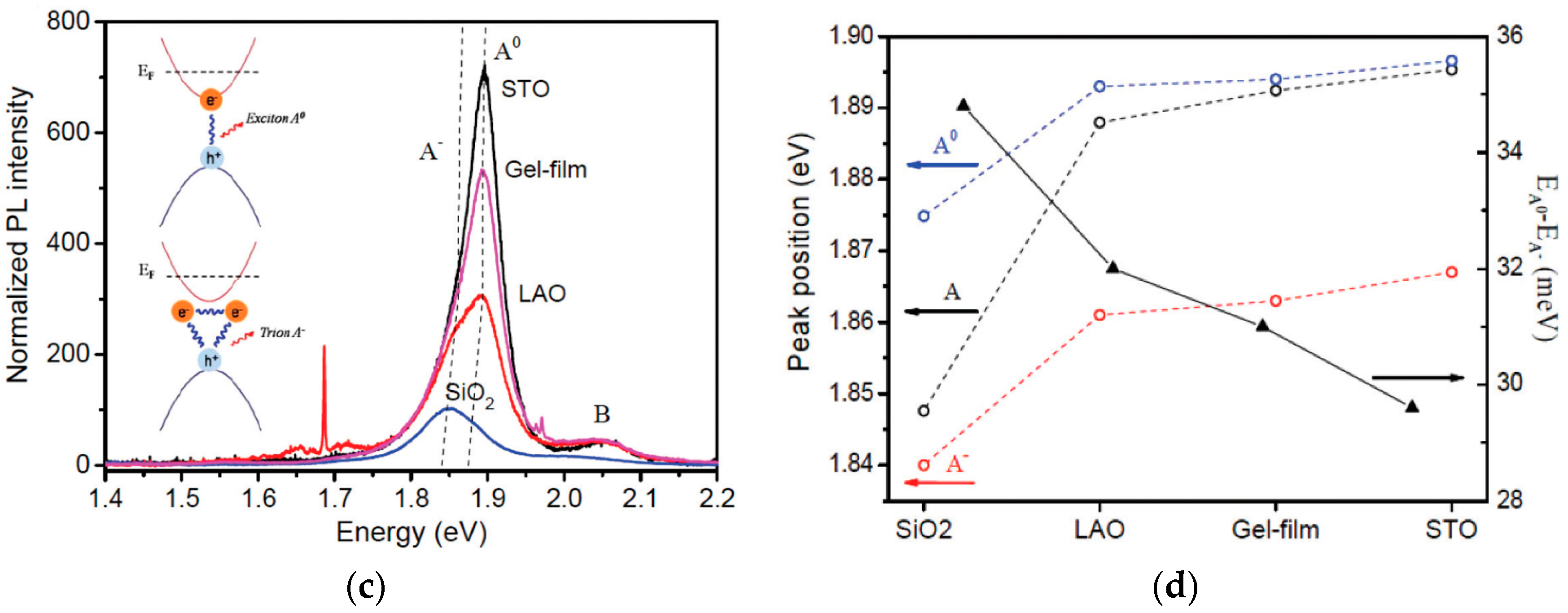
The photoluminescence (PL) properties of 2D semiconductors are also closely related to the dielectric environment. The Coulombic interaction between negatively charged electrons and positively charged holes will be modulated by dielectric screening, which further influences the binding energies and the stabilities of excitons and trions. Lin et al. studied the behaviors of these quasiparticles under different dielectric environments by using various organic solvents [20]. The whole PL peak can be divided into three peaks, representing the A− trion, A exciton, and B exciton, respectively (Figure 1a). As the dielectric constant increases, the intensities of PL peaks are rapidly enhanced, almost exponentially. As depicted in Figure 1b, the peak positions all have blue shifts in high-κ solvents, where the position of A− trion is closer to that of the A exciton, suggesting that the binding energy of trions becomes smaller. Thus the intensity ratio of trions to excitons can also be regulated by the dielectric environment. The experimental data fit well with the theoretical model. In this work, organic solvents are used to exclude the possible doping or strain effect. It is reasonable to expect that oxide dielectric substrates will have similar effects on the PL properties of 2D semiconductors.
Other effects, such as charge transfer and charge doping, also have many influences on the electrical and optical properties of 2D semiconductors [22]. Charge doping can change the types of semiconductors depending on the doping of electrons or holes. For example, at the MoS2/glass interface, the first principle calculations show that Na atoms in the glass might become donors to make the system an n-type semiconductor, while the O dangle bonds could do the opposite because of the opposite charge polarity [16]. Li et al. utilized different substrates including LaAlO3, SrTiO3, and SiO2 to control the charge transfer between a substrate and a monolayer of MoS2 [21]. A model is set up to explain how the Fermi level and work function of the substrate influence the charge transfer. Compared to a SiO2 substrate, there is a lower transfer of electrons and therefore a lower free electron density for MoS2 on a SrTiO3 substrate. As a chemical equilibrium exists between the charged and neutral excitons [23,24], the ratio of negatively charged trions to neutral excitons will decrease with a lower doping level.
Because of the larger binding energy of neutral excitons, the PL peak will have blue-shifted as there is a higher concentration of neutral excitons [25]. Studies also show that the relative proportion and intensities of neutral to charged excitons can be tuned by a gate voltage and the ambient temperature [23]. Another experiment focused on the band offset values of MoS2/high-κ interfaces, where substrate charge transfer has a similar effect on PL properties [26]. Interference has an impact on the absorption and emission intensities but has no relation to the peak position. It is also found that Raman modes are more related to the strain caused by the substrate instead of doping and dielectric screening [21]. Research on other transition-metal dichalcogenide (TMD) materials, such as MoSe2 and WS2, has shown similar properties. Currently, most reports are focused on MoS2, and thereby we mainly discuss MoS2 in this review [27,28,29].
Dielectric oxides have some other effects on 2D semiconductors, such as influencing the electron-hole recombination process. The Auger Carrier Capture Model is usually utilized to explain how defects assist the recombination of electrons and holes. Theoretical model shows that in atomic layer materials, Auger scattering is related to the strong Coulomb force inside the material [30]. Thus dielectric screening will affect the correlations of electrons and holes. Besides electrical mobility and optical luminescence, the Coulombic potential may have a further influence on electronic structures of 2D semiconductors. At higher gate voltages in MoS2, a metal-insulator transition (MIT) is observed. The electrical conductance shows a metallic behavior when the charge density is beyond 1013 cm−2 [12]. In another experiment, the results of electrical transport measurements are consistent with a variable range hopping (VRH) model. In this case, randomly distributed charges and their mutual Coulomb interaction may cause disorders in the material [10]. The top insulating layer has a dielectric capping effect on 2D semiconductors [31]. When an Al2O3 top dielectric layer is added to the black phosphorous channel, positive charges will accumulate and fix at the interface. This will result in band bending and effectively reduce the Schottky barriers at the contact.
2.2. 2D Semiconductors/Semiconducting Oxide Heterostructures
When 2D semiconductors interface with semiconducting oxides, their band alignment must be considered. Some novel phenomena, such as exciton magnetic polarons and two-dimensional electron gas, emerge in the case of large band offsets. The overall mobility is influenced by both carrier injection and scattering.
The band gap and work function are two of the most important parameters for semiconductors. The relative positions of the valence and conduction bands of two semiconductors determine the behaviors of the heterojunction. Anderson’s rule [32], quantum dipole theory [33], and other models are utilized to predict band offsets. Based on the band alignment, semiconductor heterojunctions can be classified into three types: type I (straddling or symmetric), type II (staggered gap), or type III (broken gap), as shown in the Figure 2. The heterostructure is type I if VBMA < VBMB < CBMB < CBMA, type II if VBMA < VBMB < CBMA < CBMB, and type III if VBMA < CBMA < VBMB < CBMB [34,35].
The three types of heterojunctions have been used in various devices owing to their different properties. Type I heterojunctions can well confine electrons and holes in quantum wells for more efficient electron-hole recombination [36], and therefore they are often used to generate light in optical devices such as LEDs and lasers [37]. Type II heterojunctions have very large band offsets on either conduction band or valence band and can easily confine electrons in one layer. They have been used to fabricate heterojunction field-effect transistors with high carrier mobility [38]. Both staggered gaps and broken gaps can regulate the energy difference between the valence band and the conduction band. This can affect the photon absorption and electron transition process and is applicable in photo detectors [39,40] and mid-infrared lasers [41]. In tunneling transistors [42], the type II heterojunction is utilized to enhance the tunneling current. However, in a type II junction, a finite tunneling barrier is not high enough to hinder the carrier transmission. A bigger band offset (type III heterojunction) is desirable if the carrier transmission needs to be totally reduced.
Besides these traditional applications, 2D semiconductor heterojunctions can also enable lots of novel properties including two-dimensional electron gas (2DEG), dilute magnetic oxides, and interlayer excitons. When 2D semiconductors and semiconducting oxides form heterojunctions, they will interface with each other through band alignments and their properties can be modulated by external fields. In InGaPN/GaAs heterostructures, the addition of nitrogen concentration lowers the conduction band. The original type I heterostructure changes to type II. Simultaneously, 2DEG will form at the interface [43]. In dilute magnetic semiconductors, where magnetic ions and carriers both exist in comparable strength, spin splitting and optical properties are closely related to each other. In such heterojunctions, when spin splitting of the valence induced by magnetic field exceeds the band offset in the zero field, there will be a band alignment transition. In one spin state, holes are confined to the quantum wells (type I behavior), while in the other spin state, holes will be confined to the barriers, showing type II behavior [44]. Another interesting phenomenon is interlayer excitons and polarons. At the interface of MoSe2–WSe2, bound electrons and holes are localized and stabilized in respective layers. Interlayer excitons are found to have a long lifetime of ~1.8 ns in these circumstances [45,46]. In ZnSe/(Zn,Mn)Se quantum wells, exciton magnetic polarons have been observed to have much longer lives (20ns) than in type I because of the larger band offset [47]. In the same system, calculations show that interlayer excitons have smaller binding energies and lifetimes than quantum well excitons [48].
Besides the band alignment, oxides may also inject carriers towards 2D semiconductors at the interface. This will regulate interfacial Schottky barriers as well as electrical contacts. The regulation is essential, particularly in the case of p-type MoS2 devices where holes need to be provided for electrical conduction. Chuang et al. used MoOx as contacts to fabricate p-type field effect transistors [49]. As Figure 3a shows, the substoichiometric compound MoOx (x < 3) has a high work function and its Fermi level is pinned at the valence band of MoS2. Thus holes can transport easily from MoOx to MoS2 by overcoming small Schottky barrier heights. Figure 3d shows the on and off states of the PFET device. MoOx functions as an efficient hole injector to exhibit appropriate work function and improve the contact at the interface. Different from the case of MoOx used as contacts, when MoO3 is deposited on the monolayer MoS2 as a capping layer, electron densities in the MoS2 channel will decrease because of the charge transfer effect and its overall transport properties change [50].
2.3. 2D Semiconductors/Conventional Piezoelectric Oxide Heterostructures
Piezoelectric ceramics are also usually oxides in which electric charges can be accumulated in response to external mechanical fields, or, conversely, mechanical strains can be generated in response to external electric fields. ZnO and lead zirconate titanate (PZT) are both conventional piezoelectric oxides. When piezoelectrics and 2D semiconductors form heterostructures, strain and electronic properties can have a mutual effect and one can be utilized to modulate the other property.
Piezoelectric charge accumulation at a 2D semiconductor/piezoelectric ceramic heterojunction will influence the carrier density and the electrical conductance in the 2D semiconducting channel. Chen et al. have utilized a piezoelectric ZnO nanowire to function as a gate to modulate the electrical transport behavior of MoS2 by external mechanical stimulus [51]. In FET devices, the source-drain current is usually modulated by a gate voltage. In this MoS2/ZnO system, however, environmental air pressure is instead applied for gating. When the ZnO nanowire is grown on top of an exfoliated MoS2 flake, the increase of pressure is significantly lower the source-drain current, where the ZnO nanowire functions as an effective back gate voltage: the drain current curve when Vgs = −7 V with 6.25 MPa pressure is similar to that when Vgs = −15 V without pressure. Another device is fabricated with an Al2O3 interlayer. In this device, a larger pressure induces a larger source-drain current, which is in sharp contrast to the former device. The mechanism is further explained by the piezotronic effect. At the interface of an n–n heterojunction, electrons accumulate and form a charged barrier for the balance of Fermi levels. In the ZnO–MoS2 heterostructure, free electrons accumulate to screen positive polarization charges of ZnO. Pressure will induce stronger polarization in ZnO and deplete electrons in the MoS2 channel. With an interlayer, Al2O3 functions as a capacitor dielectric layer where holes accumulate at the ZnO–Al2O3 interface and electrons accumulate at the MoS2–Al2O3 interface. Thus a larger electron concentration leads to a larger source-drain current when the polarization is enhanced by the applied pressure. In a reverse case, piezoelectricity has also been utilized in touch sensors to detect pressure based on a change in the channel current difference [52]. In ferroelectrics, strong spontaneous polarization exists and can be tuned by temperature. Fang reported a MoS2/PMN-PT composite structure, in which infrared light (IR) is used to generate heat and reduce previous polarization in ferroelectrics [53]. The charge accumulates at the interface and the carrier concentration is therefore modulated. Under such circumstances, the IR works as a negative ‘gate’ in the FET devices [53,54].
The piezoelectricity also has a great impact on the photoelectric response of 2D semiconductors. Xue et al. fabricated a p-MoS2 and an n–ZnO diode and measured its photoresponse performance under different pressures [55]. MoS2 is pretreated by SF6 to become p-type and acrylic is used to apply a pressure and simultaneously transmit the ultraviolet. The highest external quantum efficiency (EQE) is 52.7% with six layers of MoS2 at a −2 V drain voltage. The photoresponse time is much longer at low power densities, mainly because the separation of excitons in the heterojunction is slow. The barrier formed at the p–n junction interface and depleting area is crucial to stabilizing the separated photogenerated carriers [56]. When applying pressure, charges generated by piezoelectricity accumulate at the interface and lower both the valence and conduction bands of ZnO. Thus a lower barrier results in a larger depletion region, which is beneficial to optoelectronic performance. As shown in Figure 4b, the photo current and EQE both increase quickly as external pressure increases. The EQE almost quadruples at 23 MPa external mechanical stimulus. ZnO proves to be a good ‘gate’ to modulate the separation, transport, and recombination process of photocarriers. A similar experiment has been conducted at the graphene/ZnO junction with a higher Schottky barrier and a wider depletion area induced by strain, which resulted in better device performance [57].
2.4. 2D Semiconductors/Strongly Correlated Oxide Heterostructures
Strongly correlated systems are a wide range of materials where their electronic structures, magnetic properties, spin, and mechanical strain are strongly correlated with each other. The traditional band theory is based on independent electron approximation, i.e., only electron-ion interaction is considered and electron-electron interaction is ignored. However, when the interaction between electrons or spinons is not negligible, some novel phenomena such as metal-insulator transitions, spin-charge separation, and high-temperature superconductivity may appear in such strongly correlated systems. Many transition metal oxides are classified into strongly correlated materials. For example, the concept of strongly correlated Mott insulators was first proposed in NiO because its properties cannot be explained by the traditional band theory. Compared with traditional piezoelectric materials, more degrees of freedom can be utilized in strongly correlated systems. The diverse properties of strongly correlated oxides provide a variety of possibilities to modulate the properties of ultrathin 2D semiconductors; equally, 2D semiconductors can be utilized as indicators of the phase changes in strongly correlated oxides.
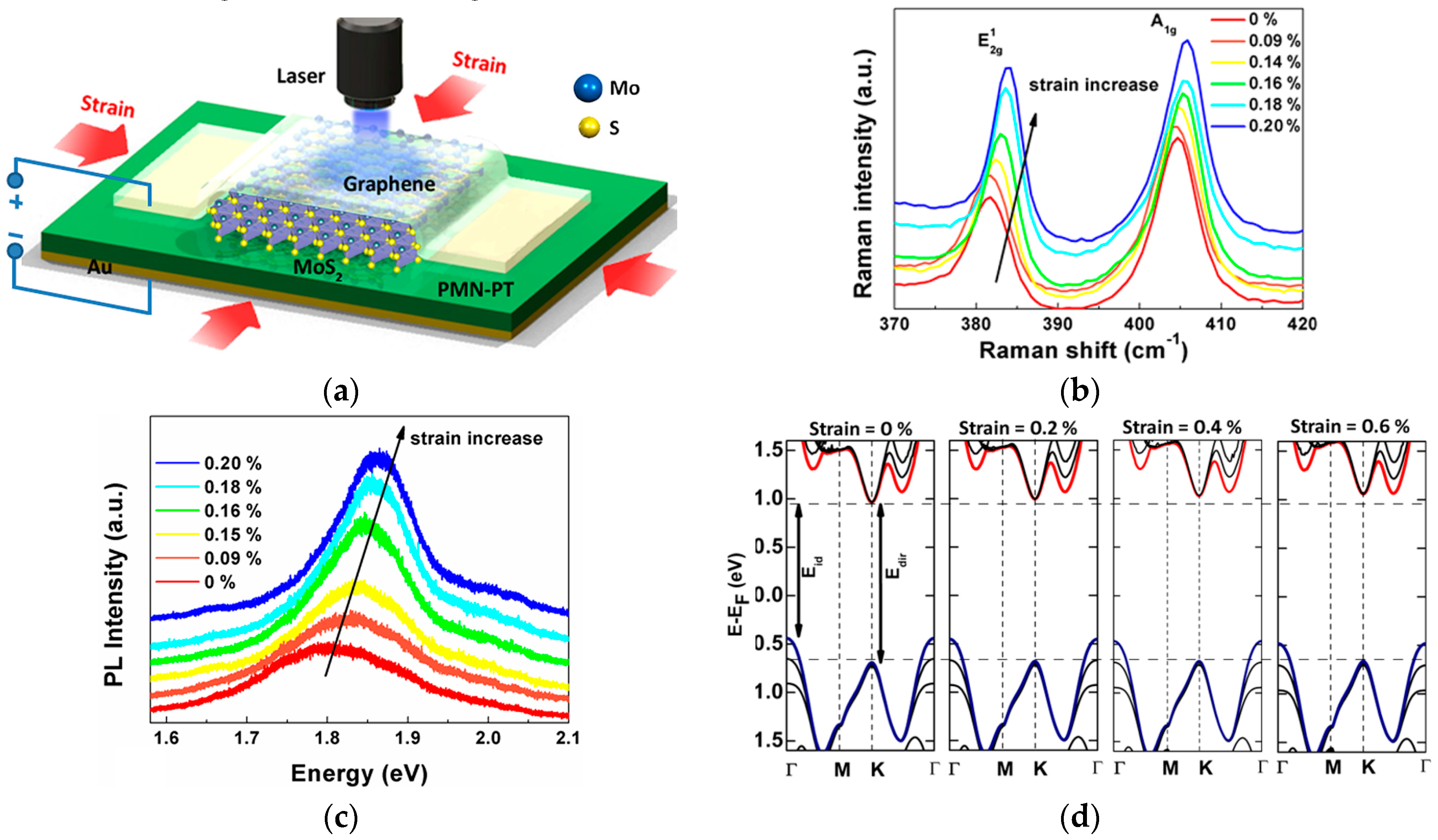
Electronic structures and band gaps of 2D semiconductors can be modulated by strongly correlated materials through strain transfer [58]. When interfacing MoS2 with PMN-PT, a new type of ferroelectric oxides, the band gap of MoS2 can be regulated through strain by applying an external voltage bias on the PMN-PT [59]. Raman spectroscopy confirms that there is a strain transfer from PMN-PT to MoS2. As shown in Figure 5c, the MoS2 PL peak blue shifts as the strain increases. A 0.2% compressive strain (corresponding to 500 V bias on PMN-PT) can shift the PL peak by 60 meV (~300 meV per 1% strain) and double the PL intensity during the process. Previous researchers have tried to explain the strain-induced change of electronic structures in MoS2 by first principle calculations [60,61,62]. As depicted in Figure 5d, both valence and conduction bands shift to higher energies with a compressive strain, and the energy levels of conduction band changed to a larger extent. At 0.2% strain, MoS2 remains an indirect semiconductor but with a larger band gap. Another study shows that the surface potential and work function of MoS2 can also be influenced by the strong polarization of ferroelectrics [63]. Because of the induced dipole effect, a work functional variation is found at the edge and interior region of PbTiO3 surface.
Strongly correlated materials have also been utilized to modulate the optical properties of 2D semiconductors. When interfacing MoS2 with VO2, which is a textbook Mott insulator and exhibits a metal-insulator transition (MIT) at around 68 °C, both the Raman and PL properties of MoS2 are strongly modulated by the VO2 substrate [64,65]. Both the E2g and A1g modes of MoS2 are thus found to have red shifts when heating the VO2 substrate to metal phase [65]. The PL position also shifts to a lower energy due to increased non-radiative electron-hole recombination. Meanwhile, the PL intensity is drastically enhanced because the excitons and trions are enhanced during the MIT process. However, Hou et al. attributed this enhancement to an optical interference effect due to the different refractive indexes of the two VO2 phases [64].
2.5. 2D Semiconductors/Magnetic Oxide Heterostructures
Ferromagnetic insulators and multiferroic oxides are two types of important magnetic oxides. Some 2D materials including graphene and MoS2 have the advantage of long diffusion lengths of spin electrons. When interfaced with functional magnetic oxides, 2D semiconductors may offer new functions and open up novel applications.
In the EuOx/graphene heterojunction, the Eu atoms will generate proximity induced ferromagnetism in graphene. Proximity-induced exchange splitting and spin orbit coupling have been revealed by first principle calculations [66]. They could also lead to a nonlinear dispersion at Γ point through inter-valley interactions [67]. Multiferroics shows the coupling between ferroelectricity and magnetism and is promising for spintronic devices. In BaMnO3/graphene structures, a distinct spin polarization is caused by the interaction between π electrons from graphene and d electrons from Mn atoms. An evident spin splitting as large as 300meV is observed in the system [68]. A high-mobility electronic region is achieved by acceptor-doping in graphene. Meanwhile, theoretical calculations have proven that multiferroic oxides can be utilized to generate 2DEG at the surface, which provides a good platform to conduct research on spin interaction and spin field effect devices [69,70,71].
It is worth noting that all of these devices are based on the advantages of the long spin diffusion length and high carrier mobility in graphene. Some other 2D semiconductors such as MoS2 possess similar advantages. Therefore, similar devices are expected to develop in 2D semiconductors with a high performance and low energy dissipation.
3. Applications of 2D Semiconductors/Functional Oxide Heterostructures
3.1. Volatile Field-Effect Transistor (FET) Devices
In modern computers, most calculations are done by a Boolean operation, which is carried out by logic gate circuits. Logic gates are mainly realized by diodes and transistors to perform as electronic switches. Compared with traditional bipolar transistors, field effect transistors (FETs) have become mainstream in practical applications because of several advantages. Bipolar transistors have majority carrier and minority carrier conduction, while in MOSFET devices only majority carriers conduct the electricity. Complementary Metal-Oxide-Semiconductor (CMOS) logic utilizes both n-channel and p-channel MOSFETs to achieve a high speed and low power consumption. Several parameters are crucial in logic operation and integrated circuits. Smaller transistor size can enhance the integration per unit area and reduce the production cost. Faster switching and response speed calls for higher mobility in channel materials and lower subthreshold swing. A high on–off ratio guarantees high performance and low leakage current. Low leakage current is also beneficial to less power dissipation.
Continuously scaling down the size of FET devices relies on the development of advanced lithography techniques and a new structure design (e.g., FinFET). As we have discussed in Section 2, short channel effect and leakage current will become big problems when the size of FETs becomes smaller. Thinning channel materials is a way to solve these problems, but in this case the existence of dangling bonds and charge traps of traditional silicon channels will hamper the mobility. Thus, novel ultrathin materials are still desired to improve the performance. A theoretical calculation based on non-equilibrium Green’s function has predicted the ultimate performance limit of MoS2 transistors [72]. This shows several merits: (i) Because the band gap of MoS2 is larger than that of silicon, the minimum current can be very small when ignoring the leakage current. The on/off ratio can reach more than 1010; (ii) Because of wave function reflection at contacts, a reduced density of states in the channel can result in a high intrinsic device transconductance (4.4 mS/μm); (iii) Subthreshold swing can be as low as 60 mV/decade (the theoretical limit) with the optimal dielectrics. For a 15-nm gate, the drain-induced barrier lowering is 10 mV/V, showing good short-channel behavior. What is more, most of the III–V semiconductors have larger mobility than MoS2 and provide better choices for high-performance transistors.
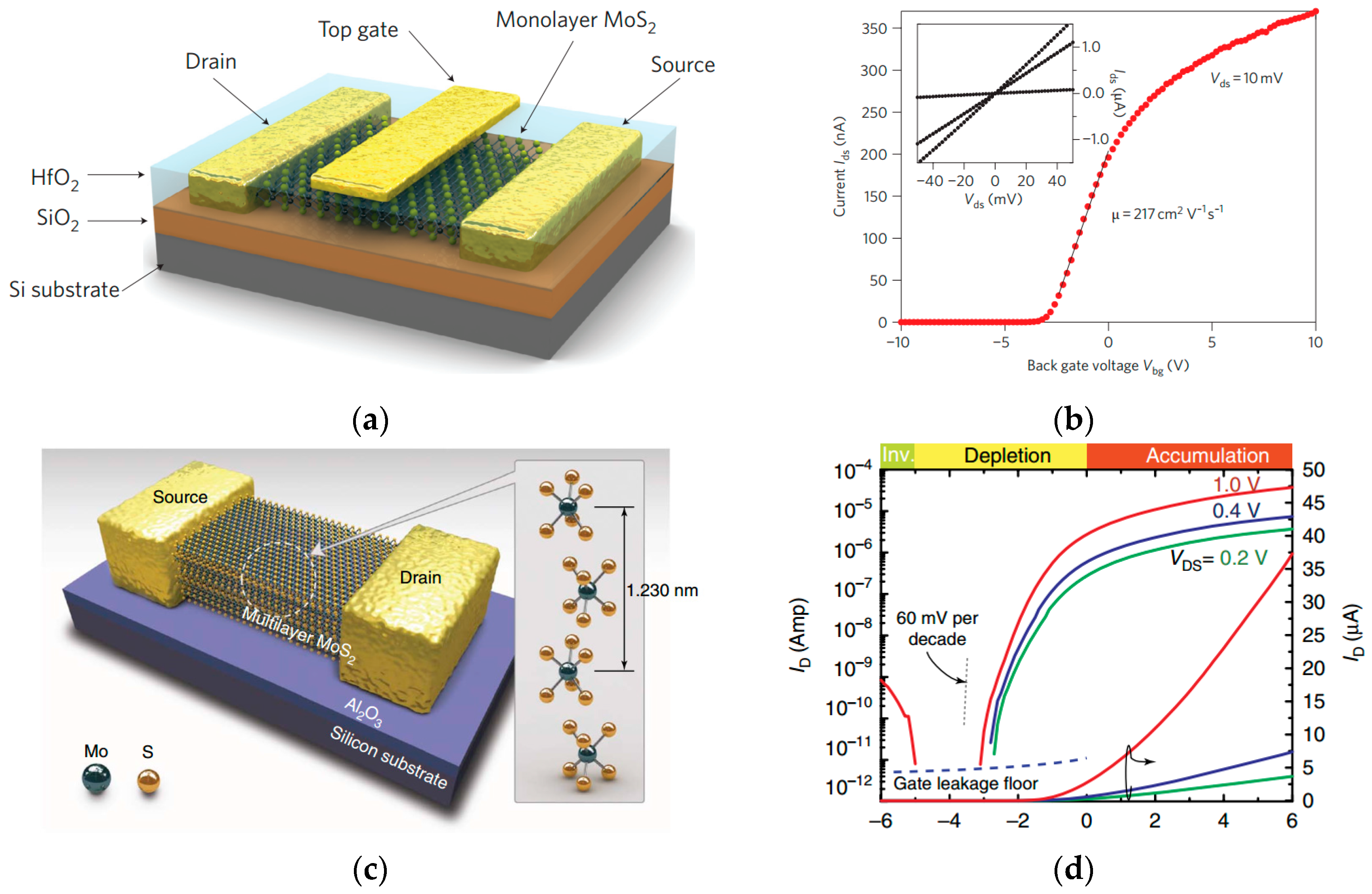
Several methods have been adopted to enhance device mobility. High-κ materials are often used as gate dielectrics [73,74]. Radisavljevic et al. used 30 nm HfO2 as a top gate and single layer MoS2 as a channel (Figure 6) [9]. At a 500 mV source drain voltage, more than 108 on–off current ratio and 1 μS/μm transconductance are achieved. The mobility is around 200 cm2V−1s−1 and the subthreshold slope is 74 mV/decade [75]. Al2O3 is also employed as a back gate to regulate multilayer MoS2. From the transfer curve shown in Figure 6d, high mobility (>100 cm2V−1s−1), a ~70 mV per decade subthreshold swing is also observed. Li et al. systematically studied the effect of the channel thickness on the overall mobility [13]. For either Ti or Au contact, 14–15 layers of MoS2 shows the best performance. The ultrathin FET channels may be strongly affected by short-range Coulombic interactions [11], and impurity density should also be considered in the devices. Oxygen molecules, water molecules, or other chemical contaminants in the ambient environment may be absorbed onto the surface and become scattering impurities. Hydrophobic substrates and dry environments are usually required for obtaining good performance of devices [76].
Interfacial contact is one of the key issues for achieving ideal transistor performance. Tunneling contacts have low Schottky barriers, but the Fermi level is likely to pin at the energy level of defects, which causes a large tunneling resistance. An ideal circumstance for MOSFETs is Ohmic contact with low resistance and matched energy levels between channels and electrodes. However, it is difficult to find metals with a suitable work function to form Ohmic contacts with channel semiconductors [72]. Some metals, such as Au, Ti [13], and Sc [77], have been employed as electrodes in the 2D semiconducting transistors, but contact problems usually exist. Many types of other non-metal electrode materials have thus been explored to solve the contact problem. For example, the high work function of MoOx pins its Fermi level at the valence band of MoS2, and holes can transport through a thin Schottky junction [49]. The situation is different in metal-semiconductor field effect transistors (MESFET), where a Schottky barrier should be apparently formed to decrease the leakage current [78]. Experiments show that higher barriers induce larger on–off current ratios and better subthreshold slopes. Meanwhile, the drain current should not be leaked to the gate. An NiOx electrode is fabricated and demonstrates a good performance, including high mobility (500–1200 cm2V−1s−1), low threshold voltage (~−1 V), low subthreshold swing (83 mV) and quick photoswitching speed (2 ms).
Compared with TMD materials, black phosphorus has a lot advantages as a volatile FET channel material. Much effort has been made to improve the performance of BP devices. BP has a moderately large band gap and much higher mobility of ~1000 cm2V−1s−1, as reported [79]. The type of contact metal and alternation of thicknesses can modulate p-type BP into n-type, with hole mobility still as high as ~950 cm2V−1s−1 [80]. BP transistors with a 20 nm channel length show a small short channel effect and still preserve an on/off ratio of 100 [81]. However, BP is unstable in air compared with other typical 2D semiconductors, which has limited its further application. The current solution is mainly to deposit an Al2O3 top gate to encapsulate the device [81,82,83]. By this method, BP can be isolated from air and current fluctuation of its devices has been effectively suppressed.
Traditionally planar thin film transistors (TFTs) are susceptible to the cracking of the used materials during bending because of the insufficient mechanical flexibility. In flexible electronics, both channel and electrode materials should have good flexibility. Liu et al. fabricated vertically aligned TFTs with indium gallium zinc oxide (IGZO) as channel materials and graphene as flexible contacts [84]. The on–off current ratio is larger than 105 and there is no evident degradation over 1000 cycles of bending. The techniques can easily be extended to 2D semiconductors. A heterojunction between BP and ZnO is used as junction FET [85]. The mechanical flexibility of BP is crucial for good interfacial contact and also has great potential in flexible devices. BP FETs on flexible polymer substrates can sustain 5000 bending cycles with unchanged properties [86]. Bessonov et al. show the potential for printed flexible electronics of MoOx/MoS2 and WOx/WS2 heterostructures [87]. Strong electrical nonlinearity and low operating voltage (0.1–0.2 V) are demonstrated with 3 nm thick ultrathin oxide dielectric layers. Compared with traditional electrostatic doping, ionic liquid gating can simultaneously provide p-doping and n-doping with a surface charge density as high as 1013 cm−2 [88]. A p–n junction is likely to form inside the semiconducting channel in the cation/anion transition region. In practical applications, transistors have to be assembled together to form complementary integrated logic circuits, which have been also demonstrated with 2D materials [89]. Wang et al. fabricated 2–12 transistors in one circuit to offer a group of functions, such as inverter, static random access memory, etc. CMOS circuits are demonstrated by Yu et al. in WSe2 with a voltage gain of about 38 and a small static dissipation [90]. Although the performance of the present devices seems good, further work still needs to be done to increase operating speeds and decrease the power dissipation for practical applications.
3.2. Nonvolatile Memory and Data Storage
Nonvolatile memory is a type of information storage mostly used in computers. Compared with volatile memory, nonvolatile memory can retain data even when power is turned off. Hard disk drives, magnetic tapes, optical discs, and flash memory are types of nonvolatile memory.
Ferroelectric random access memory (FeRAM) is a typical class of nonvolatile memory. Spontaneous polarization exists in ferroelectrics. When a coercive voltage is applied, the polarization can be triggered so as to change the on/off state of the channel. FeRAMs have many advantages such as low radiation resistance, low power consumption, and fast writing speed. Evidence supports the idea that the length of ferroelectrics can still scale down to nanometers and new device capabilities can be studied and put into use [91]. In industry, however, the difficulties lie in how to integrate FeRAM compatibly with present CMOS processes and how to produce them more effectively. Much research has been done to improve the switching speed and extend the degradation time. Ferroelectric polymer [P(VDF-TrFE)] has been integrated with MoS2 and BP to make nonvolatile memory devices and fabricate inverter circuits [92,93]. Graphene has been utilized as transparent electrodes to improve the electrical contact. The device with monolayer MoS2 possesses a mobility as high as 220 cm2V−1s−1, a subthreshold swing of 300 mV/decade, and a ~5 × 10³ write and erase current ratio [94]. The memory inverters also show a good performance and high output voltage efficiency [95].
These organic FeFETs are still limited by low operation speed, high work voltage, and short degradation time. In contrast, inorganic metal oxide ferroelectrics can produce faster memory switching and increase mechanical and thermal durability. Ko et al. utilized inorganic PZT (Pb[Zr0.2Ti0.8]O3) as gate electrodes [96]. Due to the high dielectric constant (~200) of PZT, low coercive voltage and VG (2~3 V) is observed. The low threshold voltage has the advantage of low power consumption in electronic applications. The switching curve (Figure 7c) shows a quick response and a stable performance, even under a voltage wave of 1ms duration and 10 μs ramping time. Relaxation dynamics reveals that the RC charging effect may be the reason for the switch relay, calling for a better device contact to further improve the response properties.
The duration time is a very important parameter in nonvolatile memory. As shown in Figure 7b, in the opposite direction of PZT polarization, ED, a depolarization field will be set up to suppress the polarization and lead to the instability of the memory device. High-temperature annealing and microscopic particle collision will also accelerate the process. If the dielectrics are in direct contact with metal, the internal electrical field will be fully eliminated. When the semiconductor channel is contacted with ferroelectrics, charges are mainly accumulated near the interface of metal contacts and the total depolarization field can be described as ED0/((CS/Cf) + 1), where EDO, CS, and Cf are, respectively, the original depolarization field, the capacitances of the semiconductor, and the ferroelectrics. Thus, when interfacing with ferroelectrics, 2D semiconductors have more charges accumulated at the interface compared to traditional silicon channels. As a result, the 2D semiconductor-ferroelectrics structure has a longer retention time. Its duration surpasses 2 × 10⁴ s, much better than traditional FET devices.
Spintronics opens a new dimension to explore internal properties of electrons and has a wide range of prospects in nonvolatile memory devices [97]. Rather than direct spin injection due to the tunneling effect at junctions, two-dimensional materials have the advantage of long-distance spin transport to produce nonlocal spin injection. With the help of the long diffusion length in MoS2, the spin flow can travel for a long distance without being scattered. Calculations have been done to prove that the spin transport in such structures can be electrically regulated by a gate voltage, which widens its range of applications [98]. However, a 2D semiconductor/ferromagnetic interface may still hinder the device performance because of the large Schottky barrier resistance. Chen et al. added a thin layer of MgO between Co and MoS2 [99]. The Schottky barrier height is reduced by 84%. Meanwhile, carrier depletion at the interface is alleviated and the MgO tunnel junction actually decreases the junction resistance. TiO2 is also used as the interlayer between Co and MoS2 and is found to have similar effects [100]. TiO2 of 1 nm thickness significantly lowers the Schottky barrier from 121 meV to 27 meV. The on-state current increases by ~2 orders and the device mobility increases by ~6-fold. TiO2 is also fabricated with BPs to verify the universality of this method [101]. In all three devices, the contact resistance can be regulated by gate voltage to optimize for spin injection and detection.
Theoretically, all materials with a hysteresis loop could find potential applications in nonvolatile memory devices. For instance, VO2 also possesses a hysteresis during its MIT. When interfacing MoS2 with VO2, the PL intensity of MoS2 will be enhanced or weakened during the MIT of VO2 due to an interference effect [64]. Lasers can be used to introduce additional heat at controlled positions, and the phase change can be maintained at the ambient temperature even if the laser is turned off. An optical contrast between insulating and metallic VO2 can be distinguished by the naked eye (Figure 8). Through this method, designed patterns can be written on the VO2 canvas by a laser, and the patterns would also be erased by a simple cooling-down process. The transition temperature of VO2 can be further lowered down to reduce power consumption by W-doping or other methods [102]. In this way, a nonvolatile, rewritable, contactless method of pattern writing is achieved, which opens a new way for convenient and graphic nonvolatile information storage and transfer.
3.3. Sensing and Detection
Different kinds of devices are integrated into micro-electromechanical systems. The processor is the central unit that processes data, and the transducer can transform one type of energy into another. A sensor is often used to detect a signal in the environment and turn it into an available signal, usually an electrical signal. Two-dimensional semiconductors and oxides are two good platforms for the purpose of sensing and detection. Here, based on the mechanisms of electron–hole separation in p–n junctions and photocurrent generation in phototransistors [56,103], we mainly discuss the research progress on photodetection and -conductivity in such heterojunctions. The following parameters are crucial in describing the performance of photo sensors. A sensor’s sensitivity refers to the ratio of output changes to input changes. High responsivity requires a relatively high current output and a low leakage current, guaranteeing a high on–off ratio for phototransistors. Fast electron hole separation and carrier conduction are essential to increase the switching speed. Wide sensing band and high photoelectric efficiency indicate a larger photo sensing range and a high energy conversion efficiency.
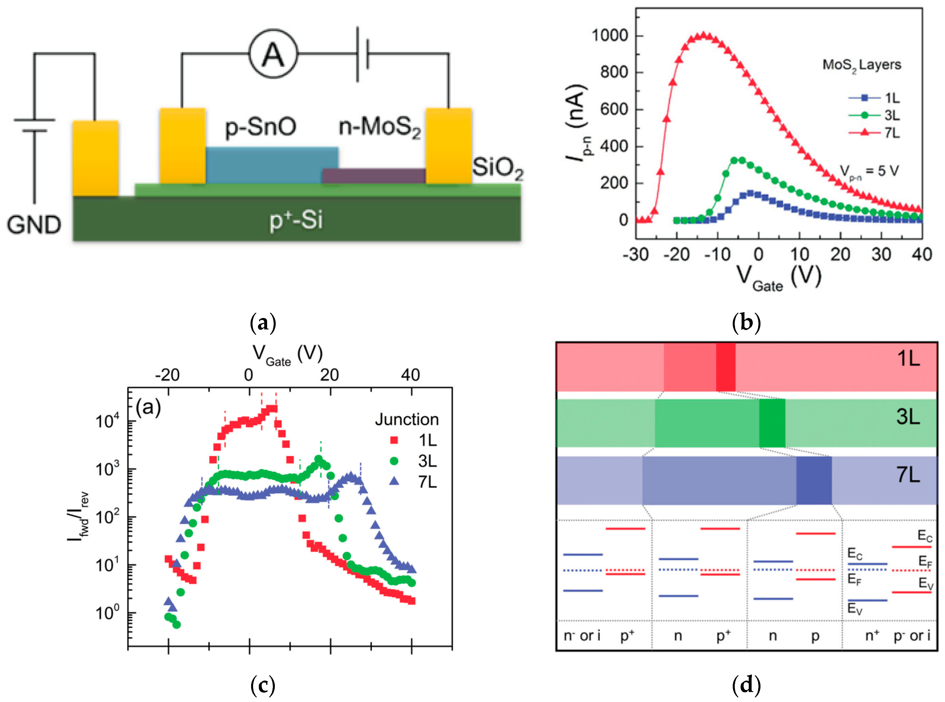
It is found that strong light–matter interaction occurs in the graphene/TMDs/graphene heterostructures [104,105]. Significantly strengthened photon absorption and electron-hole generation are also observed. Previous graphene-based photodetectors have several advantages such as wide absorption band and high speed, but weak absorption and small built-in potential limit their efficiency [106,107]. In contrast, the graphene/ZnO heterostructure can detect an ultraviolet band with a fast response in milliseconds [108]. A wide band range from ultraviolet to far-infrared and a high responsivity are also produced based on hot carrier tunneling of two graphene layers [109]. In TMD devices, vertically stacked structures provide a large response area and the intrinsic Schottky barriers guarantee an effective carrier separation. According to band diagram analysis, gate voltage can regulate the intensities and direction of photocurrents. The maximum external and internal quantum efficiency are measured to be 55% and 85%, respectively [105]. The performance can be further enhanced by improving the light absorption—for example, by adding optical resonators or plasmonic nanostructures to enhance the ambient electric fields of light [104]. Compared with 2D materials, oxides can be easily deposited with few processes and at a low cost. In SnO and at the MoS2 p–n junction, the electron–hole separation depends on the depletion area [110]. The diode can be utilized to perform a rectification (high forward to reverse current ratio as 9.3 × 10³) with a good laser response. Under different gate voltages, the junction type changes from n/p+ to n/p, and even n+/p−, thus influencing both the dark current and the photon-induced carrier separation (Figure 9d). It is worth noting that the same electron–hole separation mechanism applies to both photosensing and photovoltaic applications, so the generated photocurrent also counts in energy harvesting.
Other methods are used to further improve photodetector performance. Owing to the strong polarization and local electrostatic field (~109 V/m) of ferroelectrics, the dark current of a channel is suppressed and the power dissipation is therefore reduced [111]. At the MoS2/ferroelectrics junction, a high responsivity of 2570 A/W is obtained. The detectivity, defined as D∗ = RA1/2/(2eIdark)1/2, is 2.2 × 10¹² Jones. Another device based on MoS2/ferroelectrics heterostructures works at low temperatures. A responsivity of over 300 A/W is reached. The photoresponse range is visible to 1550 nm [112]. When the channel material is replaced by In2Se3, the photoresponse time is as fast as 200 μs [113]. To minimize environmental influence on the device performance, the MoS2 photodetector is encapsulated with atomic layer deposited HfO2 [114]. Free from ambient doping and contaminants, a lower noise and a better sensitivity are achieved. The maximum responsivity and sensitivity are 104 A/W and 7.7 × 10¹¹ Jones respectively.
Another novel application based on a photoelectric process is photoconductive switches [110]. Under a 2-mW light, the photoresponsivity (the ratio of generated photocurrent to the light power absorbed by the device channel) of BP/SrTiO3 is 2.5 A/W. The photocurrent is not volatile and the decay time is as long as several days. Red light can turn on the switch and increase the current by increasing its intensity, while UV light can turn off the switch immediately. The responsivity reaches as high as 1.1 × 10⁵ A/W, several tens of times larger than previous devices. Such a huge responsivity is attributed to the intrinsic defects in SrTiO3. Lights of different wavelengths have different optical penetration depths and could excite different donor and acceptor states in defects. UV light can generate carrier separations of different energy levels but only at the surface, which leads to the recombination of electrons and holes during the conduction. In contrast, red light can excite electrons from acceptor states through the entire sample. Instead of accumulating charges at the surface, holes can recombine at the top layer in the case of red light; as a result, the intrinsic electrical field declines and the entire conductivity increases. Therefore, lights with different wavelengths can be utilized to control the on/off states of the switch.
Similar photodetector devices have been fabricated with other 2D semiconductors. MoSe2 can be changed to p type by Nb doping to form a p–n homojunction [115]. WS2 light emitting transistors have also been demonstrated [116]. Black phosphorus could generate a greater photocurrent owing to its narrow band gap. An intrinsic 657 mA/W responsivity in the near-infrared band is reported for a 100 nm thick device [117]. In the mid-infrared light range, external responsivity is measured to be 82 A/W [118].
4. Perspectives and Challenges
So far, we have discussed lots of fundamental properties of 2D semiconductors/functional oxides heterojunctions, as well as some recent research progress on their applications. The various types of interface interactions benefit the heterojunctions in forming novel structures and providing multiple functionalities. In the future, with the miniaturization and integration of nanodevices, their applications in electronics and optoelectronics will be further enriched.
Although some novel 2D semiconductors and functional oxides have been studied for many years or even decades, there are still several challenges in the routes of their heterojunctions to practical applications. As to device fabrication, for example, the most commonly used and reliable methods are still based on the transfer technique to form vdWs heterogeneous structures. The process is facile but time-consuming, cost-ineffective, and not scalable. Further development of in situ, large-scale, and direct growth of 2D semiconductors on novel functional oxides (e.g., strongly correlated oxides) is much desired to lower the production cost and improve the performance. This is very challenging because the ambient condition in the growth of 2D semiconductors may damage the surface of these novel oxide substrates, thereby affecting the interfaces in the formed heterojunctions. Some delicately designed protecting processes should be adopted here. In the future, when more reliable and high-volume preparation of the heterojunctions is realized, their potential applications will be fully exploited.
The other challenge is to answer the following question: Are 2D semiconductors/functional oxides heterojunctions really unique or indispensable for electronic applications evaluated in the conventional figure of merits? So far most related studies have been focused on 2D electronic devices such as FET devices and p–n junctions. Lots of effort has been made to improve the mobility and speed of the devices as well as reduce their energy consumption. Promising performance has indeed been shown in several lab-made heterojunction systems. However, it will also introduce several problems in these systems, such as the instability of many 2D semiconductors (e.g., BP) and functional oxides (through losing oxygen) and susceptibility to ambient conditions (e.g., absorption of molecules in air). Overcoming these cons usually requires additional processes, which may make the 2D systems not so competitive as compared with conventional devices. In this regard, the development of 2D semiconductors/oxide systems with novel properties is a more hopeful research direction because it could provide multiple new functions that conventional devices cannot offer. For example, more dimensions of freedom in 2D semiconductors such as valley electronics have been found to be capable of regulating and carrying the information. The coupling of multiple degrees of freedom of 2D semiconductors with novel functional oxides would be a hot topic in future research.
Acknowledgments
This research was supported by Thousand Youth Talents Program of China, National Natural Science Foundation of China (51602173), the Open Research Fund Program of the State Key Laboratory of Low-Dimensional Quantum Physics (KF201603), and Tsinghua University Initiative Scientific Research Program (20161080166). We acknowledge Laura Wheatley and Inigo Howe for the proofreading of our manuscript.
Author Contributions
Kai Liu conceived the topic of this review. Zhiquan Yuan drafted the manuscript under the supervision of Kai Liu. Kai Liu and Jiwei Hou revised the manuscript.
Conflicts of Interest
The authors declare no conflict of interest.
References
- Liu, K.; Yan, Q.; Chen, M.; Fan, W.; Sun, Y.; Suh, J.; Fu, D.; Lee, S.; Zhou, J.; Tongay, S. Elastic properties of chemical-vapor-deposited monolayer MoS2, WS2, and their bilayer heterostructures. Nano Lett. 2014, 14, 5097–5103. [Google Scholar] [CrossRef] [PubMed]
- Lee, C.; Wei, X.; Kysar, J.W.; Hone, J. Measurement of the elastic properties and intrinsic strength of monolayer graphene. Science 2008, 321, 385–388. [Google Scholar] [CrossRef] [PubMed]
- Balandin, A.A.; Ghosh, S.; Bao, W.; Calizo, I.; Teweldebrhan, D.; Miao, F.; Lau, C.N. Superior thermal conductivity of single-layer graphene. Nano Lett. 2008, 8, 902–907. [Google Scholar] [CrossRef] [PubMed]
- Tongay, S.; Fan, W.; Kang, J.; Park, J.; Koldemir, U.; Suh, J.; Narang, D.S.; Liu, K.; Ji, J.; Li, J. Tuning interlayer coupling in large-area heterostructures with cvd-grown MoS2 and WS2 monolayers. Nano Lett. 2014, 14, 3185–3190. [Google Scholar] [CrossRef] [PubMed]
- Sun, Y.; Liu, K.; Hong, X.; Chen, M.; Kim, J.; Shi, S.; Wu, J.; Zettl, A.; Wang, F. Probing local strain at MX2-metal boundaries with surface plasmon-enhanced raman scattering. Nano Lett. 2014, 14, 5329–5334. [Google Scholar] [CrossRef] [PubMed]
- Wilk, G.D.; Wallace, R.M.; Anthony, J. High-κ gate dielectrics: Current status and materials properties considerations. J. Appl. Phys. 2001, 89, 5243–5275. [Google Scholar] [CrossRef]
- Osada, M.; Sasaki, T. Two-dimensional dielectric nanosheets: Novel nanoelectronics from nanocrystal building blocks. Adv. Mater. 2012, 24, 210–228. [Google Scholar] [CrossRef] [PubMed]
- Lee, Y.S.; Shim, T.H.; Yoo, S.D.; Park, J.G. Silicon thickness fluctuation scattering dependence of electron mobility in ultrathin body silicon-on-insulator n-metal-oxide-semiconductor field-effect transistors. J. Appl. Phys. 2008, 103, 084503. [Google Scholar] [CrossRef]
- Radisavljevic, B.; Radenovic, A.; Brivio, J.; Giacometti, I.V.; Kis, A. Single-layer MoS2 transistors. Nat. Nanotechnol. 2011, 6, 147–150. [Google Scholar] [CrossRef] [PubMed]
- Ghatak, S.; Pal, A.N.; Ghosh, A. Nature of electronic states in atomically thin MoS2 field-effect transistors. ACS Nano 2011, 5, 7707–7712. [Google Scholar] [CrossRef] [PubMed]
- Fivaz, R.; Mooser, E. Mobility of charge carriers in semiconducting layer structures. Phys. Rev. 1967, 163, 743. [Google Scholar] [CrossRef]
- Radisavljevic, B.; Kis, A. Mobility engineering and a metal-insulator transition in monolayer MoS2. Nat. Mater. 2013, 12, 815–820. [Google Scholar] [CrossRef] [PubMed]
- Li, S.-L.; Wakabayashi, K.; Xu, Y.; Nakaharai, S.; Komatsu, K.; Li, W.W.; Lin, Y.F.; Aparecido-Ferreira, A.; Tsukagoshi, K. Thickness-dependent interfacial coulomb scattering in atomically thin field-effect transistors. Nano Lett. 2013, 13, 3546–3552. [Google Scholar] [CrossRef] [PubMed]
- Kim, J.K.; Cho, K.; Kim, T.Y.; Pak, J.; Jang, J.; Song, Y.; Kim, Y.; Choi, B.Y.; Chung, S.; Hong, W.K. Trap-mediated electronic transport properties of gate-tunable pentacene/MoS2 pn heterojunction diodes. Sci. Rep. 2016, 6, 36775. [Google Scholar] [CrossRef] [PubMed]
- Ayari, A.; Cobas, E.; Ogundadegbe, O.; Fuhrer, M.S. Realization and electrical characterization of ultrathin crystals of layered transition-metal dichalcogenides. J. Appl. Phys. 2007, 101, 14507. [Google Scholar] [CrossRef]
- Dolui, K.; Rungger, I.; Sanvito, S. Origin of the n-type and p-type conductivity of MoS2 monolayers on a SiO2 substrate. Phys. Rev. B 2013, 87, 165402. [Google Scholar] [CrossRef]
- Hess, K.; Vogl, P. Remote polar phonon scattering in silicon inversion layers. Solid State Commun. 1979, 30, 797–799. [Google Scholar] [CrossRef]
- Kaasbjerg, K.; Thygesen, K.S.; Jauho, A.P. Acoustic phonon limited mobility in two-dimensional semiconductors: Deformation potential and piezoelectric scattering in monolayer MoS2 from first principles. Phys. Rev. B 2013, 87, 235312. [Google Scholar] [CrossRef]
- Ma, N.; Jena, D. Charge scattering and mobility in atomically thin semiconductors. Phys. Rev. X 2014, 4, 011043. [Google Scholar] [CrossRef]
- Lin, Y.; Ling, X.; Yu, L.; Huang, S.; Hsu, A.L.; Lee, Y.-H.; Kong, J.; Dresselhaus, M.S.; Palacios, T.S. Dielectric screening of excitons and trions in single-layer MoS2. Nano Lett. 2014, 14, 5569–5576. [Google Scholar] [CrossRef] [PubMed]
- Li, Y.; Qi, Z.; Liu, M.; Wang, Y.; Cheng, X.; Zhang, G.; Sheng, L. Photoluminescence of monolayer MoS2 on LaAlO3 and SrTiO3 substrates. Nanoscale 2014, 6, 15248–15254. [Google Scholar] [CrossRef] [PubMed]
- Sun, Y.; Wang, R.; Liu, K. Substrate induced changes in atomically thin 2-dimensional semiconductors: Fundamentals, engineering, and applications. Appl. Phys. Rev. 2017, 4, 011301. [Google Scholar] [CrossRef]
- Ross, J.S.; Wu, S.; Yu, H.; Ghimire, N.J.; Jones, A.M.; Aivazian, G.; Yan, J.; Mandrus, D.G.; Xiao, D.; Yao, W.; et al. Electrical control of neutral and charged excitons in a monolayer semiconductor. Nat. Commun. 2013, 4. [Google Scholar] [CrossRef] [PubMed] [Green Version]
- Mak, K.F.; He, K.; Lee, C.; Lee, G.H.; Hone, J.; Heinz, T.F.; Shan, J. Tightly bound trions in monolayer MoS2. Nat. Mater. 2013, 12, 207–211. [Google Scholar] [CrossRef] [PubMed]
- Buscema, M.; Steele, G.A.; van der Zant, H.S.; Castellanos-Gomez, A. The effect of the substrate on the raman and photoluminescence emission of single-layer MoS2. Nano Res. 2014, 7, 561–571. [Google Scholar] [CrossRef]
- Pradhan, S.K.; Xiao, B.; Pradhan, A.K. Energy band alignment of high-k oxide heterostructures at MoS2/Al2O3 and MoS2/ZrO2 interfaces. J. Appl. Phys. 2016, 120, 125305. [Google Scholar] [CrossRef]
- Zhou, P.; Xu, Q.; Li, H.; Wang, Y.; Yan, B.; Zhou, Y.; Chen, J.; Zhang, J.; Wang, K. Fabrication of two-dimensional lateral heterostructures of WS2/WO3 H2O through selective oxidation of monolayer WS2. Angew. Chem. Int. Ed. 2015, 54, 15226–15230. [Google Scholar] [CrossRef] [PubMed]
- Shim, G.W.; Yoo, K.; Seo, S.-B.; Shin, J.; Jung, D.Y.; Kang, I.-S.; Ahn, C.W.; Cho, B.J.; Choi, S.-Y. Large-area single-layer MoSe2 and its van der waals heterostructures. ACS Nano 2014, 8, 6655–6662. [Google Scholar] [CrossRef] [PubMed]
- Novoselov, K.; Mishchenko, A.; Carvalho, A.; Neto, A.C. 2D materials and van der waals heterostructures. Science 2016, 353, aac9439. [Google Scholar] [CrossRef] [PubMed]
- Wang, H.; Zhang, C.; Rana, F. Ultrafast dynamics of defect-assisted electron–hole recombination in monolayer MoS2. Nano Lett. 2014, 15, 339–345. [Google Scholar] [CrossRef] [PubMed]
- Liu, H.; Neal, A.T.; Si, M.; Du, Y.; Peide, D.Y. The effect of dielectric capping on few-layer phosphorene transistors: Tuning the schottky barrier heights. IEEE Electron Device Lett. 2014, 35, 795–797. [Google Scholar]
- Anderson, R. Germanium-gallium arsenide heterojunctions. IBM J. Res. Dev. 1960, 4, 283–287. [Google Scholar]
- Tersoff, J. Theory of semiconductor heterojunctions: The role of quantum dipoles. Phys. Rev. B 1984, 30, 4874. [Google Scholar] [CrossRef]
- Livingston, J.D. Electronic Properties of Engineering Materials; Wiley: New York, NY, USA, 1999. [Google Scholar]
- Ozcelik, V.O.; Azadani, J.G.; Yang, C.; Koester, S.J.; Low, T. Band alignment of two-dimensional semiconductors for designing heterostructures with momentum space matching. Phys. Rev. B 2016, 94. [Google Scholar] [CrossRef]
- Arakawa, Y.; Yariv, A. Quantum well lasers—Gain, spectra, dynamics. IEEE J. Quantum Electron. 1986, 22, 1887–1899. [Google Scholar] [CrossRef]
- Nakamura, S.; Senoh, M.; Iwasa, N.; Nagahama, S.-I. High-brightness ingan blue, green and yellow light-emitting diodes with quantum well structures. Jpn. J. Appl. Phys. 1995, 34, L797. [Google Scholar] [CrossRef]
- Werking, J.D.; Bolognesi, C.R.; Chang, L.-D.; Nguyen, C.; Hu, E.L.; Kroemer, H. High-transconductance InAs/AlSb heterojunction field-effect transistors with delta-doped alsb upper barriers. IEEE Electron Device Lett. 1992, 13, 164–166. [Google Scholar] [CrossRef]
- Zhang, Y.; Ma, W.; Cao, Y.; Huang, J.; Wei, Y.; Cui, K.; Shao, J. Long wavelength infrared InAs/GaSb superlattice photodetectors with InSb-like and mixed interfaces. IEEE J. Quantum Electron. 2011, 47, 1475–1479. [Google Scholar] [CrossRef]
- Howell, S.L.; Jariwala, D.; Wu, C.C.; Chen, K.S.; Sangwan, V.K.; Kang, J.; Marks, T.J.; Hersam, M.C.; Lauhon, L.J. Investigation of band-offsets at monolayer–multilayer MoS2 junctions by scanning photocurrent microscopy. Nano Lett. 2015, 15, 2278–2284. [Google Scholar] [CrossRef] [PubMed]
- Meyer, J.; Hoffman, C.; Bartoli, F.; Ram-Mohan, L. Type-II quantum-well lasers for the mid-wavelength infrared. Appl. Phys. Lett. 1995, 67, 757–759. [Google Scholar] [CrossRef]
- Koswatta, S.O.; Koester, S.J.; Haensch, W. On the possibility of obtaining MOSFET-like performance and sub-60-mV/dec swing in 1-D broken-gap tunnel transistors. IEEE Trans. Electron Devices 2010, 57, 3222–3230. [Google Scholar] [CrossRef]
- Hwang, J.S.; Lin, K.I.; Lin, H.; Hsu, S.; Chen, K.; Lu, Y.T.; Hong, Y.; Tu, C. Studies of band alignment and two-dimensional electron gas in in Ga PN/Ga AS heterostructures. Appl. Phys. Lett. 2005, 86, 061103. [Google Scholar] [CrossRef]
- Liu, X.; Petrou, A.; Warnock, J.; Jonker, B.; Prinz, G.; Krebs, J. Spin-dependent type-I, type-II behavior in a quantum well system. Phys. Rev. Lett. 1989, 63, 2280. [Google Scholar] [CrossRef] [PubMed]
- Rivera, P.; Schaibley, J.R.; Jones, A.M.; Ross, J.S.; Wu, S.; Aivazian, G.; Klement, P.; Seyler, K.; Clark, G.; Ghimire, N.J. Observation of long-lived interlayer excitons in monolayer MoSe2–WSe2 heterostructures. Nat. Commun. 2015, 6, 4985. [Google Scholar] [CrossRef] [PubMed] [Green Version]
- Chiu, M.H.; Zhang, C.; Shiu, H.W.; Chuu, C.P.; Chen, C.H.; Chang, C.Y.S.; Chen, C.H.; Chou, M.Y.; Shih, C.K.; Li, L.J. Determination of band alignment in the single-layer MoS2/WSe2 heterojunction. Nat. Commun. 2015, 6. [Google Scholar] [CrossRef] [PubMed]
- Poweleit, C.; Smith, L.; Jonker, B. Observation of long-lived exciton magnetic polarons in Zn1−xMnx Se/ZnSe multiple quantum wells. Phys. Rev. B 1994, 50, 18662. [Google Scholar] [CrossRef]
- Rossin, V.; Böttger, T.; Henneberger, F. Type-II interface exciton in ZnSe/(Zn, Mn) se heterostructures. Phys. Rev. B 1996, 54, 7682. [Google Scholar] [CrossRef]
- Chuang, S.; Battaglia, C.; Azcatl, A.; McDonnell, S.; Kang, J.S.; Yin, X.; Tosun, M.; Kapadia, R.; Fang, H.; Wallace, R.M. MoS2 p-type transistors and diodes enabled by high work function moo x contacts. Nano Lett. 2014, 14, 1337–1342. [Google Scholar] [CrossRef] [PubMed]
- Lin, J.; Zhong, J.; Zhong, S.; Li, H.; Zhang, H.; Chen, W. Modulating electronic transport properties of MoS2 field effect transistor by surface overlayers. Appl. Phys. Lett. 2013, 103, 063109. [Google Scholar] [CrossRef]
- Chen, L.; Xue, F.; Li, X.; Huang, X.; Wang, L.; Kou, J.; Wang, Z.L. Strain-gated field effect transistor of a MoS2–ZnO 2D–1D hybrid structure. ACS Nano 2015, 10, 1546–1551. [Google Scholar] [CrossRef] [PubMed]
- Park, W.; Yang, J.H.; Kang, C.G.; Lee, Y.G.; Hwang, H.J.; Cho, C.; Lim, S.K.; Kang, S.C.; Hong, W.K.; Lee, S.K. Characteristics of a pressure sensitive touch sensor using a piezoelectric pvdf-trfe/MoS2 stack. Nanotechnology 2013, 24, 475501. [Google Scholar] [CrossRef] [PubMed]
- Fang, H.; Lin, Z.; Wang, X.; Tang, C.Y.; Chen, Y.; Zhang, F.; Chai, Y.; Li, Q.; Yan, Q.; Chan, H.L.W.; et al. Infrared light gated MoS2 field effect transistor. Opt. Express 2015, 23, 31908–31914. [Google Scholar] [CrossRef] [PubMed]
- Hsieh, C.-Y.; Chen, Y.-T.; Tan, W.-J.; Chen, Y.-F.; Shih, W.Y.; Shih, W.-H. Graphene-lead zirconate titanate optothermal field effect transistors. Appl. Phys. Lett. 2012, 100, 113507. [Google Scholar] [CrossRef]
- Xue, F.; Chen, L.; Chen, J.; Liu, J.; Wang, L.; Chen, M.; Pang, Y.; Yang, X.; Gao, G.; Zhai, J. P-type MoS2 and n-type zno diode and its performance enhancement by the piezophototronic effect. Adv. Mater. 2016, 17, 3391–3398. [Google Scholar] [CrossRef] [PubMed]
- Furchi, M.M.; Polyushkin, D.K.; Pospischil, A.; Mueller, T. Mechanisms of photoconductivity in atomically thin MoS2. Nano Lett. 2014, 14, 6165–6170. [Google Scholar] [CrossRef] [PubMed]
- Liu, S.; Liao, Q.; Lu, S.; Zhang, Z.; Zhang, G.; Zhang, Y. Strain modulation in graphene/zno nanorod film schottky junction for enhanced photosensing performance. Adv. Funct. Mater. 2016, 26, 1347–1353. [Google Scholar] [CrossRef]
- Meng, L.; Zhang, Y.; Hu, S.; Wang, X.; Liu, C.; Guo, Y.; Wang, X.; Yan, X. Two dimensional WS2 lateral heterojunctions by strain modulation. Appl. Phys. Lett. 2016, 108, 263104. [Google Scholar] [CrossRef]
- Hui, Y.Y.; Liu, X.; Jie, W.; Chan, N.Y.; Hao, J.; Hsu, Y.T.; Li, L.J.; Guo, W.; Lau, S.P. Exceptional tunability of band energy in a compressively strained trilayer MoS2 sheet. ACS Nano 2013, 7, 7126–7131. [Google Scholar] [CrossRef] [PubMed]
- Scalise, E.; Houssa, M.; Pourtois, G.; Afanas, V.; Stesmans, A. First-principles study of strained 2D MoS2. Phys. E Low Dimens. Syst. Nanostruct. 2014, 56, 416–421. [Google Scholar] [CrossRef]
- Peelaers, H.; Van de Walle, C.G. Effects of strain on band structure and effective masses in MoS2. Phys. Rev. B 2012, 86, 241401. [Google Scholar] [CrossRef]
- Scalise, E.; Houssa, M.; Pourtois, G.; Afanas’ev, V.; Stesmans, A. Strain-induced semiconductor to metal transition in the two-dimensional honeycomb structure of MoS2. Nano Res. 2012, 5, 43–48. [Google Scholar] [CrossRef]
- Hye-Jin, J.; Woo Young, Y.; Jo, W. Control of work function of MoS2 with ferroelectric polarization in honeycomb-like heterostructure. Appl. Phys. Lett. 2017, 110, 191601. [Google Scholar] [CrossRef]
- Hou, J.; Wang, X.; Fu, D.; Ko, C.; Chen, Y.; Sun, Y.; Lee, S.; Wang, K.X.; Dong, K.; Sun, Y.; et al. Modulating photoluminescence of monolayer molybdenum disulfide by metal-insulator phase transition in active substrates. Small 2016, 12, 3976–3984. [Google Scholar] [CrossRef] [PubMed]
- Lin, Y.C.; DeLello, K.; Zhang, H.T.; Zhang, K.; Lin, Z.; Terrones, M.; Engel-Herbert, R.; Robinson, J.A. Photoluminescence of monolayer transition metal dichalcogenides integrated with VO2. J. Phys. Condens. Matter 2016, 28, 504001. [Google Scholar] [CrossRef] [PubMed]
- Su, S.; Barlas, Y.; Lake, R.K. Proximity induced quantum anomalous hall effect in graphene/euo hetero-structures. arXiv, 2015; arXiv:1509.06427. [Google Scholar]
- Su, S.; Barlas, Y.; Li, J.; Shi, J.; Lake, R.K. Effect of intervalley interaction on band topology of commensurate graphene/euo heterostructures. Phys. Rev. B 2017, 95, 075418. [Google Scholar] [CrossRef]
- Zanolli, Z. Graphene-multiferroic interfaces for spintronics applications. Sci. Rep. 2016, 6, 31346. [Google Scholar] [CrossRef] [PubMed]
- Jia, C.; Berakdar, J. Multiferroic oxides-based flash memory and spin-field-effect transistor. Appl. Phys. Lett. 2009, 95, 012105. [Google Scholar] [CrossRef]
- Jia, C.; Berakdar, J. Magnetotransport and spin dynamics in an electron gas formed at oxide interfaces. Phys. Rev. B 2011, 83, 045309. [Google Scholar] [CrossRef]
- Jia, C.-L.; Berakdar, J. Functionalization of Multiferroic Oxide Structures for Spintronic Devices. In Proceedings of the International Society for Optics and Photonics, Orlando, FL, USA, 5–9 April 2010; p. 76030O-1. [Google Scholar]
- Yoon, Y.; Ganapathi, K.; Salahuddin, S. How good can monolayer MoS2 transistors be? Nano Lett. 2011, 11, 3768–3773. [Google Scholar] [CrossRef] [PubMed]
- Kingon, A.I.; Maria, J.-P.; Streiffer, S. Alternative dielectrics to silicon dioxide for memory and logic devices. Nature 2000, 406, 1032–1038. [Google Scholar] [CrossRef] [PubMed]
- Chander, S.; Baishya, S. A two-dimensional gate threshold voltage model for a heterojunction soi-tunnel fet with oxide/source overlap. IEEE Electron Device Lett. 2015, 36, 714–716. [Google Scholar] [CrossRef]
- Kim, S.; Konar, A.; Hwang, W.-S.; Lee, J.H.; Lee, J.; Yang, J.; Jung, C.; Kim, H.; Yoo, J.-B.; Choi, J.-Y. High-mobility and low-power thin-film transistors based on multilayer MoS2 crystals. Nat. Commun. 2012, 3, 1011. [Google Scholar] [CrossRef] [PubMed]
- Bao, W.; Cai, X.; Kim, D.; Sridhara, K.; Fuhrer, M.S. High mobility ambipolar MoS2 field-effect transistors: Substrate and dielectric effects. Appl. Phys. Lett. 2013, 102, 042104. [Google Scholar] [CrossRef]
- Das, S.; Chen, H.-Y.; Penumatcha, A.V.; Appenzeller, J. High performance multilayer MoS2 transistors with scandium contacts. Nano Lett. 2012, 13, 100–105. [Google Scholar] [CrossRef] [PubMed]
- Lee, H.S.; Baik, S.S.; Lee, K.; Min, S.-W.; Jeon, P.J.; Kim, J.S.; Choi, K.; Choi, H.J.; Kim, J.H.; Im, S. Metal semiconductor field-effect transistor with MoS2/conducting NiOx van der waals schottky interface for intrinsic high mobility and photoswitching speed. ACS Nano 2015, 9, 8312–8320. [Google Scholar] [CrossRef] [PubMed]
- Li, L.; Yu, Y.; Ye, G.J.; Ge, Q.; Ou, X.; Wu, H.; Feng, D.; Chen, X.H.; Zhang, Y. Black phosphorus field-effect transistors. Nat. Nanotechnol. 2014, 9, 372–377. [Google Scholar] [CrossRef] [PubMed]
- Perello, D.J.; Chae, S.H.; Song, S.; Lee, Y.H. High-performance n-type black phosphorus transistors with type control via thickness and contact-metal engineering. Nat. Commun. 2015, 6. [Google Scholar] [CrossRef] [PubMed]
- Miao, J.; Zhang, S.; Cai, L.; Scherr, M.; Wang, C. Ultrashort channel length black phosphorus field-effect transistors. ACS Nano 2015, 9, 9236–9243. [Google Scholar] [CrossRef] [PubMed]
- Avsar, A.; Vera-Marun, I.J.; Tan, J.Y.; Watanabe, K.; Taniguchi, T.; Castro Neto, A.H.; Ozyilmaz, B. Air-stable transport in graphene-contacted, fully encapsulated ultrathin black phosphorus-based field-effect transistors. ACS Nano 2015, 9, 4138–4145. [Google Scholar] [CrossRef] [PubMed]
- Na, J.; Lee, Y.T.; Lim, J.A.; Hwang, D.K.; Kim, G.-T.; Choi, W.K.; Song, Y.-W. Few-layer black phosphorus field-effect transistors with reduced current fluctuation. ACS Nano 2014, 8, 11753–11762. [Google Scholar] [CrossRef] [PubMed]
- Liu, Y.; Zhou, H.; Cheng, R.; Yu, W.; Huang, Y.; Duan, X. Highly flexible electronics from scalable vertical thin film transistors. Nano Lett. 2014, 14, 1413–1418. [Google Scholar] [CrossRef] [PubMed]
- Jeon, P.J.; Lee, Y.T.; Lim, J.Y.; Kim, J.S.; Hwang, D.K.; Im, S. Black phosphorus–zinc oxide nanomaterial heterojunction for p–n diode and junction field-effect transistor. Nano Lett. 2016, 16, 1293–1298. [Google Scholar] [CrossRef] [PubMed]
- Zhu, W.; Yogeesh, M.N.; Yang, S.; Aldave, S.H.; Kim, J.-S.; Sonde, S.; Tao, L.; Lu, N.; Akinwande, D. Flexible black phosphorus ambipolar transistors, circuits and am demodulator. Nano Lett. 2015, 15, 1883–1890. [Google Scholar] [CrossRef] [PubMed]
- Bessonov, A.A.; Kirikova, M.N.; Petukhov, D.I.; Allen, M.; Ryhänen, T.; Bailey, M.J. Layered memristive and memcapacitive switches for printable electronics. Nat. Mater. 2015, 14, 199. [Google Scholar] [CrossRef] [PubMed]
- Xu, H.; Fathipour, S.; Kinder, E.W.; Seabaugh, A.C.; Fullerton-Shirey, S.K. Reconfigurable ion gating of 2H-MoTe2 field-effect transistors using poly (ethylene oxide)-CsCLO4 solid polymer electrolyte. ACS Nano 2015, 9, 4900–4910. [Google Scholar] [CrossRef] [PubMed]
- Wang, H.; Yu, L.; Lee, Y.-H.; Shi, Y.; Hsu, A.; Chin, M.L.; Li, L.-J.; Dubey, M.; Kong, J.; Palacios, T. Integrated circuits based on bilayer MoS2 transistors. Nano Lett. 2012, 12, 4674–4680. [Google Scholar] [CrossRef] [PubMed]
- Yu, L.; Zubair, A.; Santos, E.J.; Zhang, X.; Lin, Y.; Zhang, Y.; Palacios, T.S. High-performance WSe2 complementary metal oxide semiconductor technology and integrated circuits. Nano Lett. 2015, 15, 4928–4934. [Google Scholar] [CrossRef] [PubMed]
- Ahn, C.; Rabe, K.; Triscone, J.-M. Ferroelectricity at the nanoscale: Local polarization in oxide thin films and heterostructures. Science 2004, 303, 488–491. [Google Scholar] [CrossRef] [PubMed]
- Lee, Y.T.; Hwang, D.K.; Im, S. High-performance a MoS2 nanosheet-based nonvolatile memory transistor with a ferroelectric polymer and graphene source-drain electrode. J. Korean Phys. Soc. 2015, 67, L1499–L1503. [Google Scholar] [CrossRef]
- Lee, Y.T.; Hwang, D.K.; Choi, W.K. High-performance black phosphorus top-gate ferroelectric transistor for nonvolatile memory applications. J. Korean Phys. Soc. 2016, 69, 1347–1351. [Google Scholar] [CrossRef]
- Lee, H.S.; Min, S.W.; Park, M.K.; Lee, Y.T.; Jeon, P.J.; Kim, J.H.; Ryu, S.; Im, S. MoS2 nanosheets for top-gate nonvolatile memory transistor channel. Small 2012, 8, 3111–3115. [Google Scholar] [CrossRef] [PubMed]
- Lee, Y.T.; Kwon, H.; Kim, J.S.; Kim, H.-H.; Lee, Y.J.; Lim, J.A.; Song, Y.W.; Yi, Y.; Choi, W.K.; Hwang, D.K.; et al. Nonvolatile ferroelectric memory circuit using black phosphorus nanosheet-based field-effect transistors with P(VDF-TrFE) polymer. ACS Nano 2015, 9, 10394–10401. [Google Scholar] [CrossRef] [PubMed]
- Ko, C.; Lee, Y.; Chen, Y.; Suh, J.; Fu, D.; Suslu, A.; Lee, S.; Clarkson, J.D.; Choe, H.S.; Tongay, S.; et al. Ferroelectrically gated atomically thin transition-metal dichalcogenides as nonvolatile memory. Adv. Mater. 2016, 28, 2923–2930. [Google Scholar] [CrossRef] [PubMed]
- Su, G.; Wu, X.; Tong, W.; Duan, C. Two-dimensional layered materials-based spintronics. SPIN 2015, 5. [Google Scholar] [CrossRef]
- Li, H.; Shao, J.; Yao, D.; Yang, G. Gate-voltage-controlled spin and valley polarization transport in a normal/ferromagnetic/normal MoS2 junction. ACS Appl. Mater. Interfaces 2014, 6, 1759–1764. [Google Scholar] [CrossRef] [PubMed]
- Chen, J.-R.; Odenthal, P.M.; Swartz, A.G.; Floyd, G.C.; Wen, H.; Luo, K.Y.; Kawakami, R.K. Control of schottky barriers in single layer MoS2 transistors with ferromagnetic contacts. Nano Lett. 2013, 13, 3106–3110. [Google Scholar] [CrossRef] [PubMed]
- Dankert, A.; Langouche, L.; Kamalakar, M.V.; Dash, S.P. High-performance molybdenum disulfide field-effect transistors with spin tunnel contacts. ACS Nano 2014, 8, 476–482. [Google Scholar] [CrossRef] [PubMed]
- Kamalakar, M.V.; Madhushankar, B.N.; Dankert, A.; Dash, S.P. Low schottky barrier black phosphorus field-effect devices with ferromagnetic tunnel contacts. Small 2015, 11, 2209–2216. [Google Scholar] [CrossRef] [PubMed]
- Lee, S.; Cheng, C.; Guo, H.; Hippalgaonkar, K.; Wang, K.; Suh, J.; Liu, K.; Wu, J. Axially engineered metal–insulator phase transition by graded doping VO2 nanowires. J. Am. Chem. Soc. 2013, 135, 4850–4855. [Google Scholar] [CrossRef] [PubMed]
- Yin, Z.; Li, H.; Li, H.; Jiang, L.; Shi, Y.; Sun, Y.; Lu, G.; Zhang, Q.; Chen, X.; Zhang, H. Single-layer MoS2 phototransistors. ACS Nano 2011, 6, 74–80. [Google Scholar] [CrossRef] [PubMed]
- Britnell, L.; Ribeiro, R.M.; Eckmann, A.; Jalil, R.; Belle, B.D.; Mishchenko, A.; Kim, Y.-J.; Gorbachev, R.V.; Georgiou, T.; Morozov, S.V.; et al. Strong light-matter interactions in heterostructures of atomically thin films. Science 2013, 340, 1311–1314. [Google Scholar] [CrossRef] [PubMed]
- Yu, W.J.; Liu, Y.; Zhou, H.; Yin, A.; Li, Z.; Huang, Y.; Duan, X. Highly efficient gate-tunable photocurrent generation in vertical heterostructures of layered materials. Nat. Nanotechnol. 2013, 8, 952–958. [Google Scholar] [CrossRef] [PubMed]
- Echtermeyer, T.J.; Britnell, L.; Jasnos, P.K.; Lombardo, A.; Gorbachev, R.V.; Grigorenko, A.N.; Geim, A.K.; Ferrari, A.C.; Novoselov, K.S. Strong plasmonic enhancement of photovoltage in graphene. Nat. Commun. 2011, 2, 458. [Google Scholar] [CrossRef] [PubMed]
- Liu, Y.; Cheng, R.; Liao, L.; Zhou, H.; Bai, J.; Liu, G.; Liu, L.; Huang, Y.; Duan, X. Plasmon resonance enhanced multicolour photodetection by graphene. Nat Commun. 2011, 2, 579. [Google Scholar] [CrossRef] [PubMed]
- Nie, B.; Hu, J.G.; Luo, L.B.; Xie, C.; Zeng, L.H.; Lv, P.; Li, F.Z.; Jie, J.S.; Feng, M.; Wu, C.Y. Monolayer graphene film on ZnO nanorod array for high-performance schottky junction ultraviolet photodetectors. Small 2013, 9, 2872–2879. [Google Scholar] [CrossRef] [PubMed]
- Liu, C.-H.; Chang, Y.-C.; Norris, T.B.; Zhong, Z. Graphene photodetectors with ultra-broadband and high responsivity at room temperature. Nat. Nanotechnol. 2014, 9, 273–278. [Google Scholar] [CrossRef] [PubMed]
- Wang, Z.; He, X.; Zhang, X.X.; Alshareef, H.N. Hybrid van der waals p–n heterojunctions based on SnO and 2D MoS2. Adv. Mater. 2016, 28, 9133–9141. [Google Scholar] [CrossRef] [PubMed]
- Wang, X.; Wang, P.; Wang, J.; Hu, W.; Zhou, X.; Guo, N.; Huang, H.; Sun, S.; Shen, H.; Lin, T. Ultrasensitive and broadband MoS2 photodetector driven by ferroelectrics. Adv. Mater. 2015, 27, 6575–6581. [Google Scholar] [CrossRef] [PubMed]
- Chen, Y.; Wang, X.; Wang, P.; Huang, H.; Wu, G.; Tian, B.; Hong, Z.; Wang, Y.; Sun, S.; Sheng, H.; et al. Optoelectronic properties of few-layer MoS2 fet gated by ferroelectric relaxor polymer. ACS Appl. Mater. Interfaces 2016. [Google Scholar] [CrossRef] [PubMed]
- Wu, G.; Wang, X.; Wang, P.; Huang, H.; Chen, Y.; Sun, S.; Shen, H.; Lin, T.; Wang, J.; Zhang, S.; et al. Visible to short wavelength infrared In2Se3-nanoflake photodetector gated by a ferroelectric polymer. Nanotechnology 2016, 27, 364002. [Google Scholar] [CrossRef] [PubMed]
- Kufer, D.; Konstantatos, G. Highly sensitive, encapsulated MoS2 photodetector with gate controllable gain and speed. Nano Lett. 2015, 15, 7307–7313. [Google Scholar] [CrossRef] [PubMed]
- Jin, Y.; Keum, D.H.; An, S.J.; Kim, J.; Lee, H.S.; Lee, Y.H. A van der waals homojunction: Ideal p–n diode behavior in MoSe2. Adv. Mater. 2015, 27, 5534–5540. [Google Scholar] [CrossRef] [PubMed]
- Jo, S.; Ubrig, N.; Berger, H.; Kuzmenko, A.B.; Morpurgo, A.F. Mono-and bilayer WS2 light-emitting transistors. Nano Lett. 2014, 14, 2019–2025. [Google Scholar] [CrossRef] [PubMed]
- Youngblood, N.; Chen, C.; Koester, S.J.; Li, M. Waveguide-integrated black phosphorus photodetector with high responsivity and low dark current. Nat. Photonics 2015, 9, 247–252. [Google Scholar] [CrossRef]
- Guo, Q.; Pospischil, A.; Bhuiyan, M.; Jiang, H.; Tian, H.; Farmer, D.; Deng, B.; Li, C.; Han, S.-J.; Wang, H. Black phosphorus mid-infrared photodetectors with high gain. Nano Lett. 2016, 16, 4648–4655. [Google Scholar] [CrossRef] [PubMed]
Figure 1.
MoS2 PL properties influenced by dielectric environment and charge doping. (a) A typical PL spectrum of single-layer MoS2 that is fitted with three peaks. The inset schematics demonstrate classical pictures of a trion and an exciton; (b) PL peak positions as a function of surrounding solvent dielectric constants (Yuxuan Lin et al. [20]); (c) PL spectra of monolayer MoS2 on SiO2, LaAlO3, gel-film, and SrTiO3 substrates; (d) Peak positions of PL peak (A), neutral excitons emission (A0), and trion emission (A−), and energy difference between neutral excitons emission (A0) and trion emission (A−) (Yuanyuan Li et al. [21]).
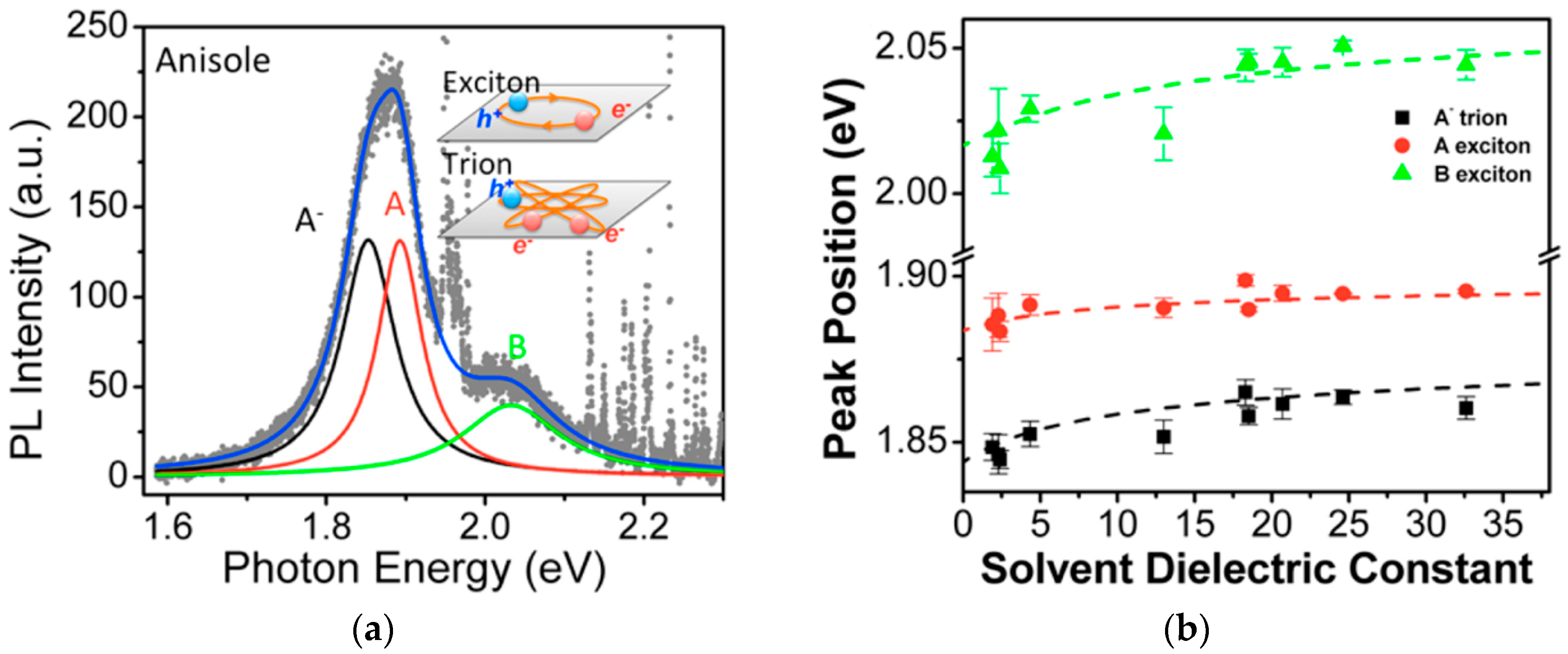

Figure 2.
Illustration of type I, II, and III semiconducting heterostructures.
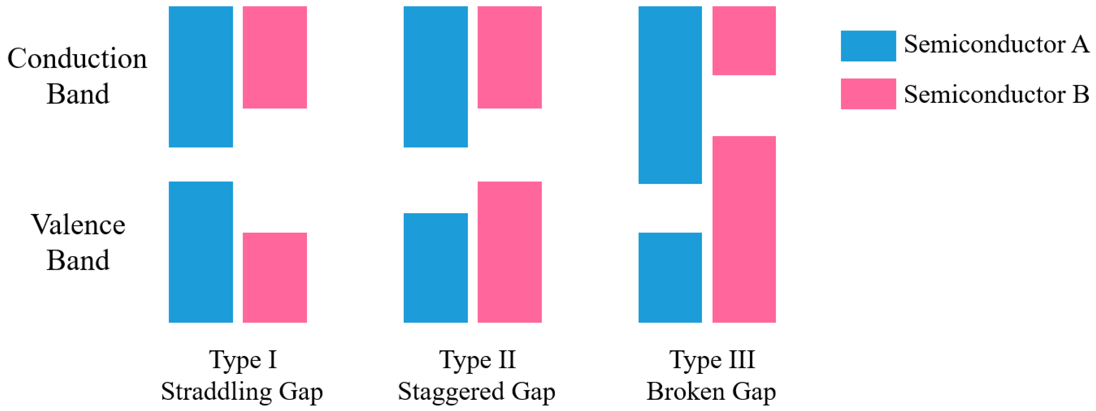
Figure 3.
MoS2/MoOx heterojunction. (a) Valence and conduction band positions with respect to vacuum level for MoS2, WSe2, Pd, and MoOx; (b) Schematic of the device structure; (c) Ids vs. Vgs characteristics for a representative MoS2 PFET with MoOx contacts; (d) Qualitative band diagrams for the ON (top panel) and OFF (bottom panel) states of the MoS2 PFET (Steven Chuang et al. [49]).
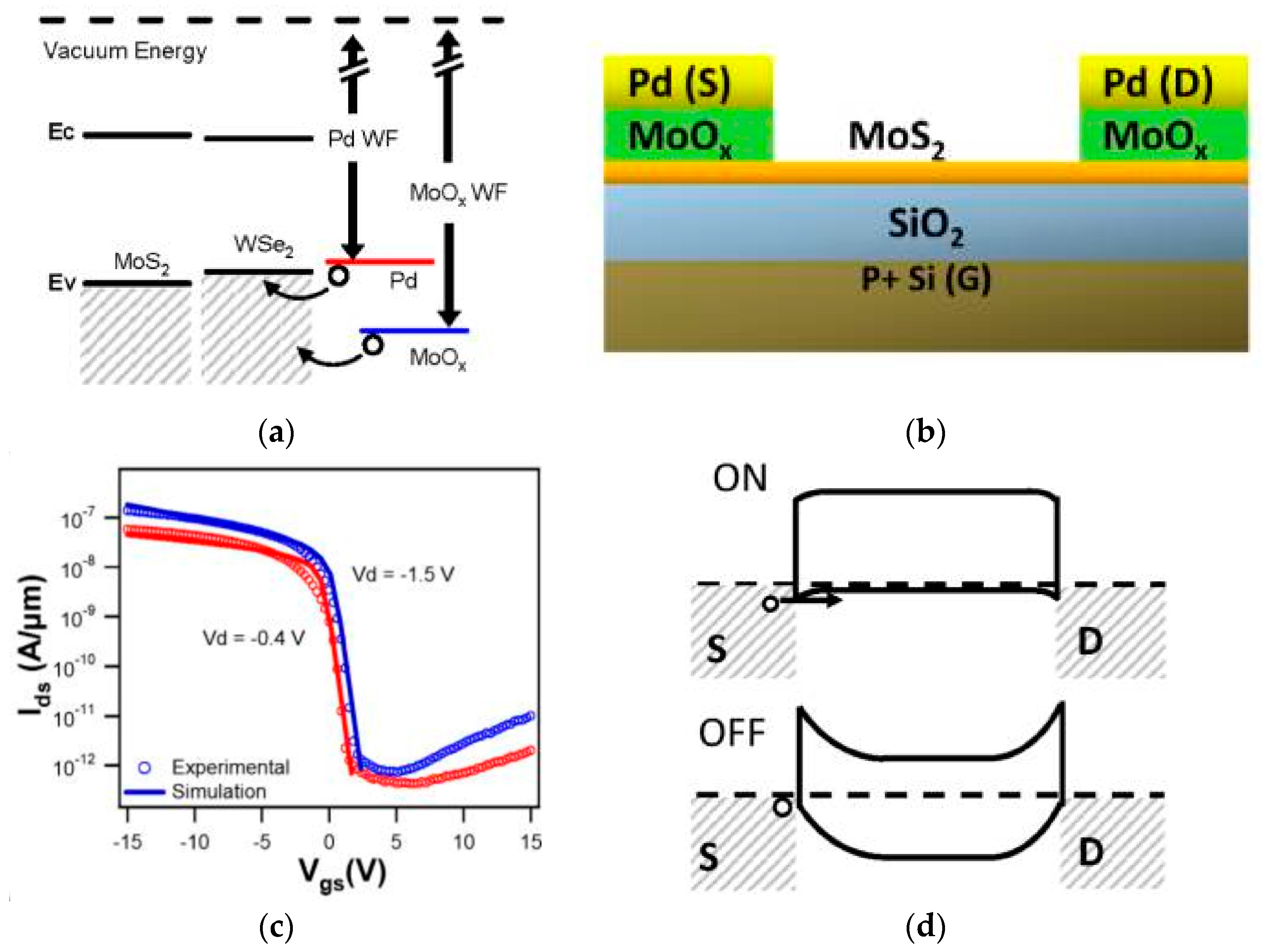
Figure 4.
Photoelectric response of a 2D semiconductor/piezoelectric ceramic heterostructure. (a) Schematic of experimental set-up for testing the diode; (b) Pressure dependence of Iph at a drain bias of –2 V and an incident power density of 500 mW cm−2. The inset shows the increased EQE with the increased applied pressure; (c) Band diagrams interpreting photogenerated carriers and piezophototronic effect enhanced photocurrents (Fei Xue et al. [55]).
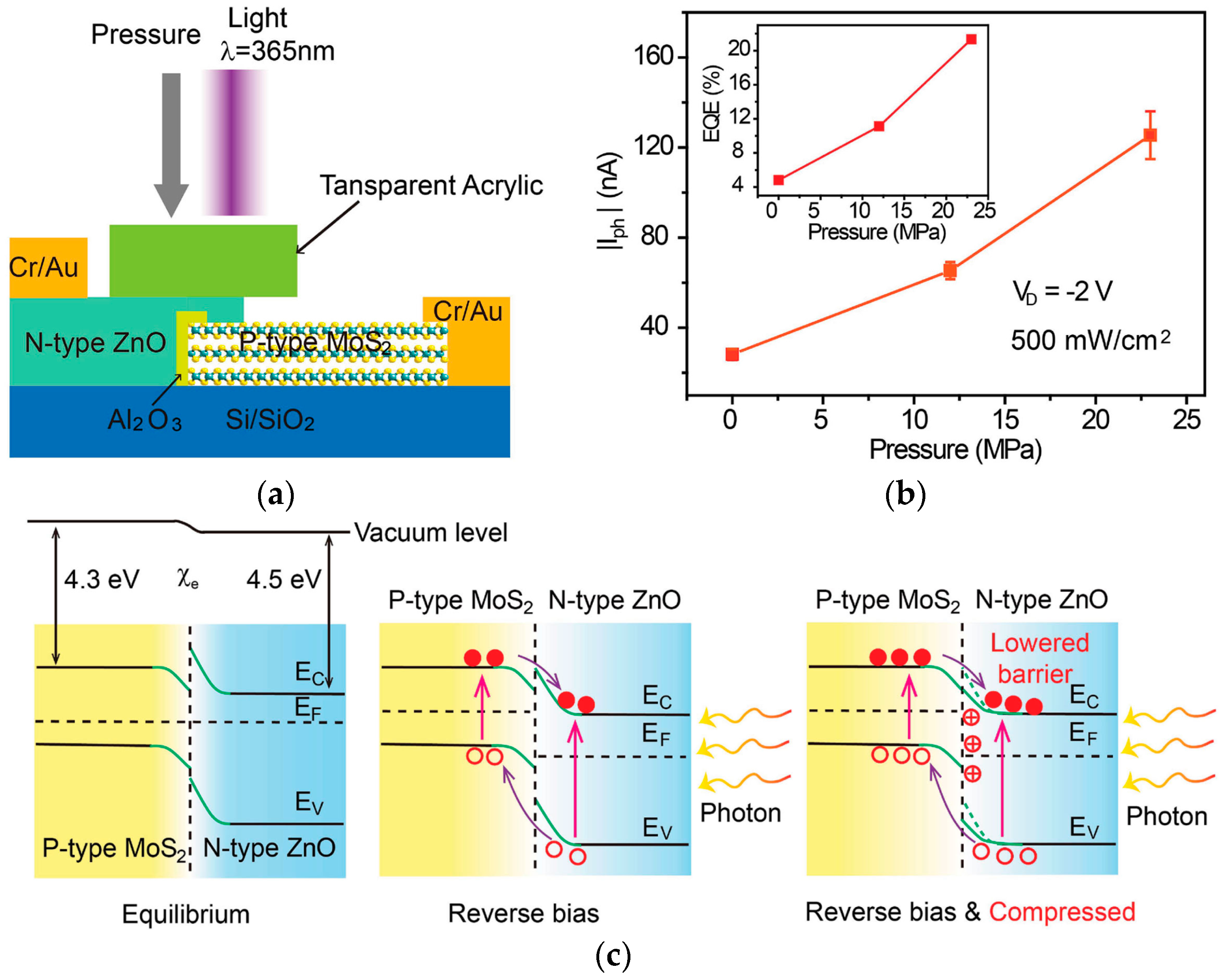
Figure 5.
Electronic structure and band gap of a 2D semiconductor influenced by strongly correlated materials through strain transfer. (a) Schematic diagram of Raman and PL measurements on MoS2. MoS2 is sandwiched between a piezoelectric PMN-PT substrate and a graphene top electrode; (b) Raman spectra of a trilayer MoS2 under various applied strains; (c) PL spectra of MoS2 under various strains; (d) Band structures of ABA-BAB stacking trilayer MoS2 under 0.0%, 0.2%, 0.4%, and 0.6% biaxial compressive strain (Yeung Yu Hui et al. [59]).

Figure 6.
Schematics and performance of monolayer and multilayer MoS2 transistors. (a) Schematic of MoS2 monolayer transistors; (b) Room-temperature transfer characteristic for an FET with a 10 mV applied bias voltage Vds. Inset: Ids–Vds curve acquired for Vbg values of 0, 1 and 5 V (Branimir Radisavljevic et al. [9]); (c) Schematic of a MoS2 thin film transistors with a multilayer MoS2 crystal; (d) Drain current versus back gate voltage, showing a ~106 on/off ratio and ~80 mV per decade subthreshold slope (Sunkook Kim et al. [75]).

Figure 7.
Nonvolatile memory produced by inorganic FeFETs. (a) Device schematic of the 2D TMD/PZT heterostructure; (b) ED in an isolated PZT thin film and in a sandwich structure with metal electrodes; (c) ID versus time curves of on and off states with different sets of voltage pulse parameters: peak voltage (VP), width (tw), and edge (te); (d) A series of relaxation curves immediately after pulsed gating at on (down-polarized, P↓) states and off (up-polarized, P↑) states at various tw and te (Changhyun Ko et al. [96]).
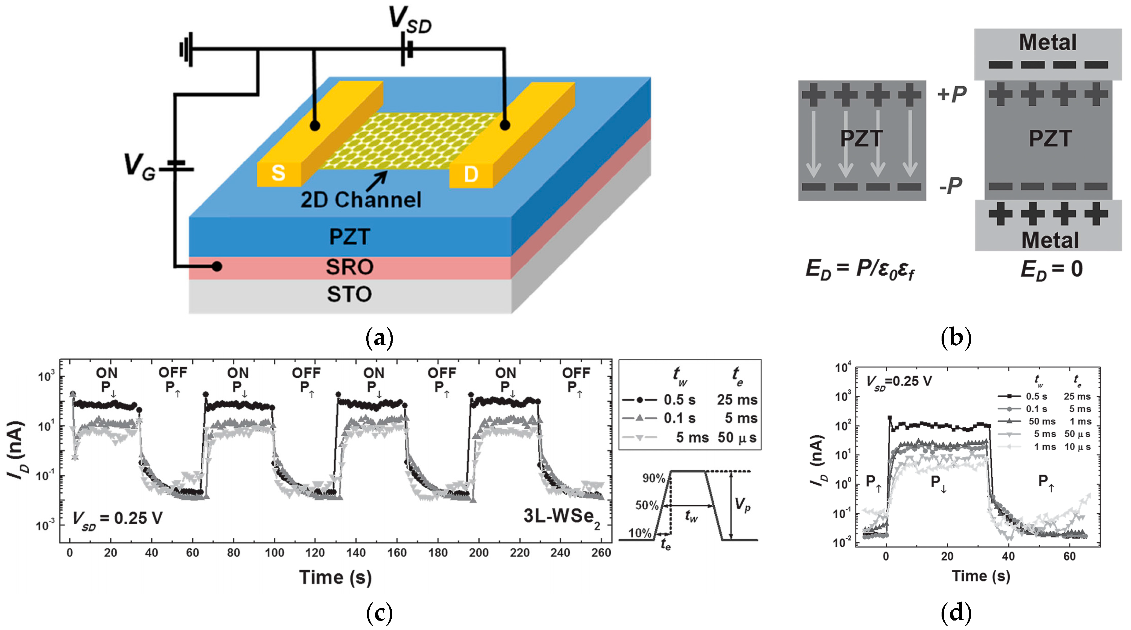
Figure 8.
Writing and erasing desired patterns on VO2 to modulate the PL intensity of MoS2. (a) Temperature dependence of electrical conductance of a typical VO2 film; (b) Laser-writing induced metallic regions with a shape of “2” on an insulating VO2 film covered by a MoS2 monolayer; (c) Laser writing a metallic VO2 circle, which enhances the PL intensity of the overlayer MoS2 (Jiwei Hou et al. [64]).
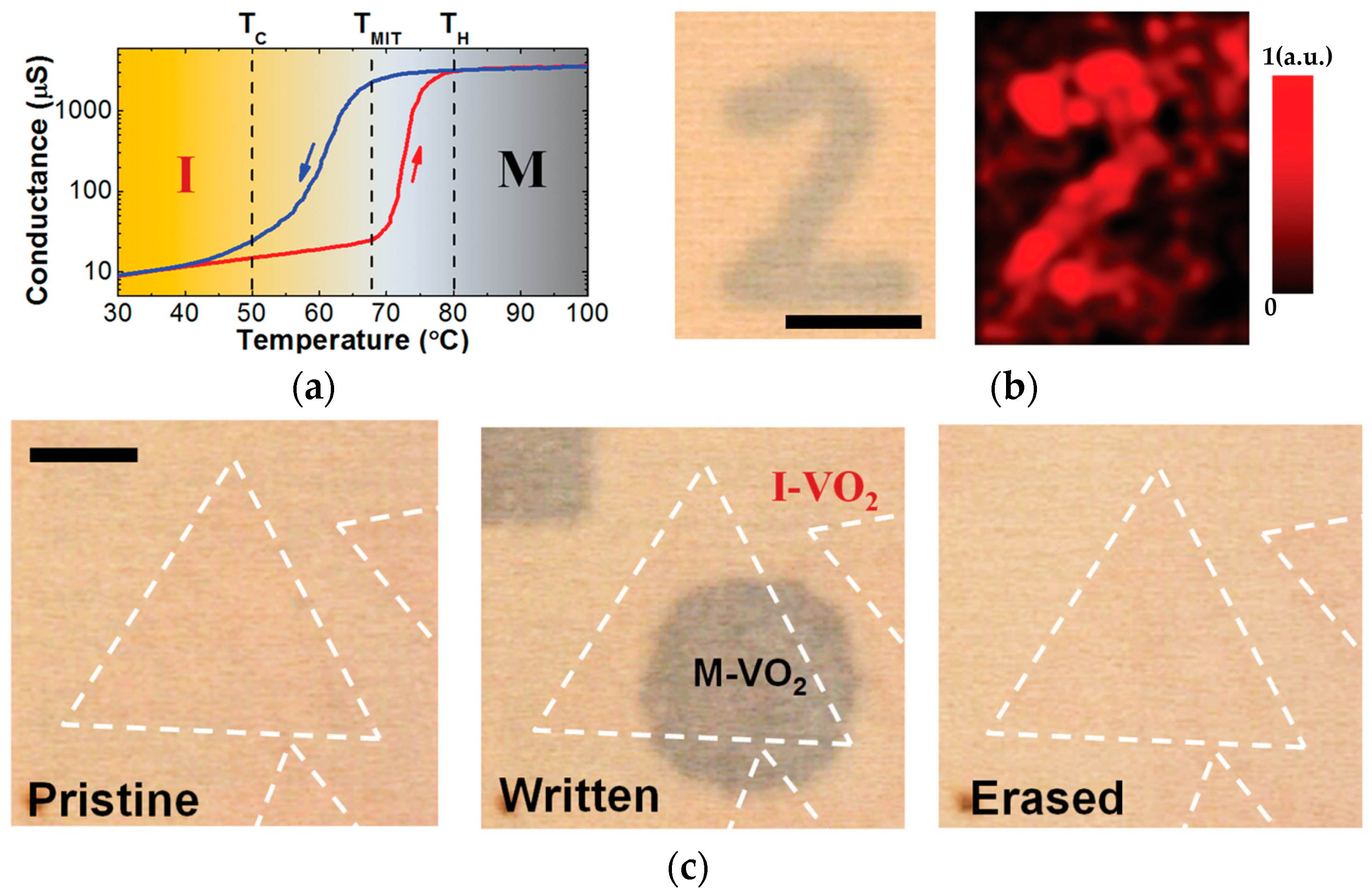
Figure 9.
Rectification effect in MoS2/SnO p–n diodes. (a) Schematic illustration for the setup of gate-tunable I–V characterization; (b) Anti-ambipolar transfer curves for all three junctions; (c) Rectification ratio of the 1 L, 3 L, and 7 L heterojunctions as a function of gate voltage; (d) Illustration of the band alignments according to the change in rectification ratio (Zhenwei Wang et al. [110]).

© 2017 by the authors. Licensee MDPI, Basel, Switzerland. This article is an open access article distributed under the terms and conditions of the Creative Commons Attribution (CC BY) license (http://creativecommons.org/licenses/by/4.0/).
Share and Cite
MDPI and ACS Style
Yuan, Z.; Hou, J.; Liu, K. Interfacing 2D Semiconductors with Functional Oxides: Fundamentals, Properties, and Applications. Crystals 2017, 7, 265. https://doi.org/10.3390/cryst7090265
AMA Style
Yuan Z, Hou J, Liu K. Interfacing 2D Semiconductors with Functional Oxides: Fundamentals, Properties, and Applications. Crystals. 2017; 7(9):265. https://doi.org/10.3390/cryst7090265
Chicago/Turabian StyleYuan, Zhiquan, Jiwei Hou, and Kai Liu. 2017. "Interfacing 2D Semiconductors with Functional Oxides: Fundamentals, Properties, and Applications" Crystals 7, no. 9: 265. https://doi.org/10.3390/cryst7090265
Note that from the first issue of 2016, this journal uses article numbers instead of page numbers. See further details here.