
Heteroepitaxy, an Amazing Contribution of Crystal Growth to the World of Optics and Electronics

Air Force Research Laboratory, Sensors Directorate, WPAFB, Dayton, OH 45433, USA
Crystals 2017, 7(6), 178; https://doi.org/10.3390/cryst7060178
Submission received: 21 April 2017
/
Revised: 5 June 2017
/
Accepted: 11 June 2017
/
Published: 19 June 2017
Abstract
:Advances in Electronics and Optics are often preceded by discoveries in Crystal Growth theory and practice. This article represents in retrospect some of the most significant contributions of heteroepitaxy in these and some other areas—the strong impact of the three modes of heteroepitaxy on microelectronics and quantum optics, the big “push” of PENDEO epitaxy in development of Light Emitting Diodes, etc. A large part of the text is dedicated to heteroepitaxy of nonlinear optical materials grown on orientation-patterned templates and used in the development of new quasi-phase-matching frequency conversion laser sources. By achieving new frequency ranges such sources will result in a wide variety of applications in areas such as defense, security, industry, medicine, and science. Interesting facts from the scientific life of major contributors in the field are mixed in the text with fine details from growth experiments, chemical equations, results from material characterizations and some optical and crystallographic considerations—all these presented in a popular way but without neglecting their scientific importance and depth. The truth is that often heteroepitaxy is not just the better but the only available option. The truth is that delays in device development are usually due to gaps in materials research. In all this, miscommunication between different scientific communities always costs vain efforts, uncertainty, and years of going in a wrong scientific direction. With this article we aim to stimulate a constructive dialog that could lead to solutions of important interdisciplinary scientific and technical issues.

1. Introduction
Like many others this story starts at an unexpected time and place. The time is about a year or two before the beginning of World War II and the place is a small office in the basement of Iowa State College. John Atanasoff, a young professor with a bachelor degree in materials science, a master’s in mathematics, and a doctorate in theoretical physics, was spending the long winter evenings of 1937–1938 in vain attempts to realize one of his old ideas. Still working on his PhD thesis, Atanasoff had experienced serious computing problems—no matter that his Monroe calculator was one of the best at that time, it was still working so slowly so he had to spend hours and hours in boring calculations. Then, several years later, it was still about the same. The current experiments with vacuum tubes, radio signals and various electronic devices also required time consuming heavy calculations. The idea to help himself by developing his own computing machine without the problems of the existing analog devices—working slowly with accuracy that is strongly dependent upon the performance of each one of their parts—started to obsess him again, more and more, but... with not much success.
“... One cold winter night, frustrated after so many discouraging events, John got into his car and started driving without any destination. 200 miles later, he pulled onto a roadside somewhere in the state of Illinois. Here, he continued thinking about the creation of the machine and, as the rumor says, he had a drink of bourbon. No longer nervous and tense, he realized that his thoughts were coming together clearly”.[1]
In March 1939 after receiving a grant of $650, Atanasoff was ready to embark in the exciting adventure to build an entirely digital machine. He hired Clifford Berry—a bright electrical engineering student, and from 1939 until 1941 they worked on developing their Atanasoff-Berry Computer (ABC). ABC had the size of a big desk (Figure 1a), weighed 750 pounds and featured rotating drums for memory consisting of hundreds of capacitors. It had also 300 glowing vacuum tubes and a read/write system that recorded numbers by scorching marks on cards. However, ABC had also all major features of last generation superpower computers—a binary system of arithmetic, separate memory and computing functions, regenerative memory, parallel processing, electronic amplifiers, clocked control of electronic operations, and a modular design. In 1997, to pay tribute to the late inventors, a team of researchers, engineers, faculty members, retired faculties and students from Iowa State University and Ames Laboratory built a working replica of ABC. The project took four years and cost nearly $350. This money compared to the $650 that John and Clifford had in 1939 (equivalent to only $8K in 1997) is an indication of the passion that Atanasoff and Berry had and their hard work. The computers today are, of course, incomparably faster and much more powerful. As for prices and sizes some of them, like Raspberry Pi [2], can be as small as the credit card that we could use to buy them on-line for the ridiculous price of … $5 (Figure 1b).
What has made these and many other “miracles” possible in the time frame of a human life only? Obviously, memorable events like the demonstration in 1947 of the first semiconductor transistor (Figure 1c). However, a closer look under the ordinary engineering surface will reveal dozens of examples of great discoveries in crystal growth theory and practice that are the real reason for the rapid progress in the last a hundred years or so—a period that starts in the dawn of the crystal growth theory. The following paragraphs are dedicated to some of them.
2. The Growth Modes of Heteroepitaxy
In 1939, about the same time when Atanasoff and Berry were working on their ABC, six thousand miles east of Iowa State College somewhere on the Balkans, another ambitious professor from the Department of Physical Chemistry of Sofia University, Ivan Stranski (Ivan is the Slavic translation of John) and his brilliant former student and co-worker now, Lubomir Krastanov, continued to be interested in heteroepitaxy. They were well-grounded with what had already been done in the field so they had a great deal of thoughts about the two well-known cases of heteroepitaxy—the two-dimensional (2D) layer-by-layer growth—the so-called Frank–Van der Merwe (FM) mode, and the three-dimensional (3D) island growth, known as Volmer–Weber (VW) mode. However, they felt that something was missing. For example, they wondered what pulls the trigger of converting one smooth at the beginning 2D layer-by-layer (FM) growth in a rough at the end 3D island (VW) growth. They believed that the so-called “half-crystal position”, introduced by them, called “kink” now, played somehow an important role in explanation of these processes. The unicity of this position is that one can increase or decrease the crystal size simply by successive, reversible attachments or detachments of atoms at the kink site, and no change in the surface energy will take place. At the same time the energy released at an act of attachment will be exactly equal to three times the single work of separation, i.e., , as far as three neighboring units are always involved in this case—one from the raw, one from the plane, and one from the crystal. The work of separation from this position is also equal to the lattice energy of the crystal per building unit and taken with opposite sign chemical potential µ, i.e.:
In the case of heteroepitaxy, i.e., when a crystal material (marked with a “prim”) grows on another, substrate material, there are two possibilities: (i) when , then the gradient of the chemical potential in the growth direction is positive, i.e., and the growth of the “prim” material, being energetically favored, will result in a smooth 2D-type surface morphology (Figure 2a); and (ii) when and , then the growth will be rather 3D-type island growth (Figure 2b).
To obtain more information Stranski and Krastanov tried to look at the half-crystal position from a different angle. When a foreign (unlike or “prim”) atom attaches to the substrate surface this atom will be connected in a vertical (normal) and a horizontal (lateral) direction. This arrangement allows the energy released after the attachment at the half-crystal position to be expressed differently, as:
Here and denote the lateral and the normal energies released after bonding the approaching atom with the half atomic row, the half crystal plane and the half underlying crystal block. This expression is more informative because now we replace the underlying crystal block by another block from a different crystal material. Thus, the lateral bonding with the two neighbors from the row and from the plane will remain about the same as in the case of homoepitaxy. However, the normal bonding (the one across the interface) will be changed and the changed total work of separation at this single act of attachment will be:
Now by adding and extracting the single work of separation , Equation (3) converts in:
Here is the single work of separation of unlike (foreign, or “prim”) particles, while is the single work of separation for identical (own) particles. By having in the formula, it is easily to say that, if , then and the equilibrium vapor pressure of the first monolayer on the foreign substrate will be smaller than the equilibrium vapor pressure of the bulk crystal , i.e., . Then at least one monolayer can be deposited at any vapor pressure that is higher than even at under saturation with respect to the bulk crystal. In the opposite case, the opposite is true, and a higher supersaturation is required [4].
Developing further this idea, Stranski and Krastanov concluded that after the 2D layer-by-layer growth of several monolayers, at a certain critical thickness (which depends on the lattice mismatch between the film and the substrate), 3D islands will start to appear on the film surface and the growth will continue three-dimensionally. The same idea can be equivalently formulated as island formation on the top of a wetting layer with thickness-dependent surface energy. This approach allows the critical wet layer thickness to be ab initio calculated [5,6]. The formation of the 3D islands is accompanied with the formation of some edge dislocations within them, created in response to the need to reduce the strain between the substrate and the film [7]. This intermediate Stranski–Krastanov (SK) “layer-plus-island growth” (Figure 2c), is one of the three known modes of heteroepitaxy classified later, in 1958, by Ernst Bauer [8].
Meantime scientists and engineers put them into practice. From this point there is only a little step to the invention of the first transistor that soon will replace all 300 glowing vacuum tubes in ABC and “shrink” the Electronics to Microelectronics. The three modes of heteroepitaxy, however, are of great importance not only for Electronics but for Optics as well. Today the SK mode is widely used in the theory and practices of the formation of quantum dots (Figure 3a) [9] and the FM mode—in the quantum wells (Figure 3b) [10]. A typical example is [11] where the authors evaluate the wetting layer and its temperature dependence in order to determine the optimal conditions for self-assembly of InAs/GaAs quantum dots.
3. III-Nitrides
3.1. Heteroepitaxy of III-Nitrides
III-Nitrides, such as GaN and AlN, due to their wideband structure, high thermal conductivity, high melting point, and high resistivity to chemicals are among the most preferable materials for high power, high frequency, and high temperature electronics; and for bright, shorter wavelength emitters in the LED technology. These materials, however, cannot be grown from melt because of their high vapor pressure and do not have their own templates so the only option for them is heteroepitaxy. There are a number of articles proposing different traditional [12] or more exotic [13] substrate options. The most proposed substrates for GaN are sapphire, SiC, and AlN, but the problem with the last one is the same—AlN itself does not have its own templates. SiC is expensive and has quite different thermal expansion, which means “expect troubles” especially at thick layer growth. The cheap and readily available sapphire seems to be the best heteroepitaxial option for thin or thick GaN growth. However, the lattice mismatch between GaN and sapphire is huge, 33% (Figure 4), which makes “the mission almost impossible”. One elegant solution, which for a long time now is a practice in the semiconductor industry, is to nitride first the sapphire surface with ammonia and after that to deposit a thin low temperature GaN buffer layer. While the buffer layer aims to reduce the stress between two different materials, the purpose of the nitridation is to form a thin AlN layer prior to the deposition of the GaN layer:
The expectation is that due to the smaller lattice mismatch between AlN and GaN, 2.5%, GaN can be grown more easily on AlN than on sapphire. However, a new problem arises. The in-plane lattice mismatch between AlN (0001) and sapphire (0001) is also large, even larger, 35%. Fortunately, when AlN (0001) grows on sapphire (0001), it naturally rotates at 30° (Figure 4) around its c-axis with respect to sapphire. This rotation reduces the AlN/sapphire lattice mismatch from 33% to 13.3% so AlN grows on sapphire.
Metal Organic Chemical Vapor Deposition (MOCVD) growths of high quality GaN using an AlN buffer layer were performed still in the mid-80s by Amano [15] who also realized growth of AlGaN and GaInN ternary alloys [16].Growth of GaN using a low temperature GaN buffer layer was performed first by Nakamura [17] who also reported the highest at the time Hall mobility of GaN.
3.2. Nano- and Micro-Heteroepitaxy
Instead of using a low temperature buffer layer, there are other ways to relieve the strain between the sapphire substrate and the growing GaN layer, for example, by the so-called AGOG (Aluminum, Growth, Oxide, Grain) approach [18,19]. The AGOG approach consists of the next steps: (i) coating the sapphire surface with a thin Al layer; (ii) making a pattern—as shown on Figure 5a the pattern is composed of many 400 nm × 400 nm × 100 nm miniature square mesas; (iii) treating the film, first at lower temperature (450 °C) to oxidize it, i.e., to turn the mesas into polycrystalline Al2O3 (Figure 5b), and after that at higher temperature (1250 °C) to convert the mesas into crystalline form (Figure 5c). The AGOG technique enables the hard steps of polishing and patterning the resistant sapphire surface to be avoided, or to nitride it. Moreover, the sapphire islands act as springs that can reduce the strain and eventually facilitate the separation of the film from the substrate.
Strain induced by different lattice parameters and different thermal properties may offer an additional degree of freedom for tailoring materials, but this is often at the expense of dislocation generation and even cracking of the growing layer. Recently, eliminating some of the drawbacks, a low temperature 3D vertical epitaxial growth of micrometer-scale defect-free Ge and SiGe crystals on Si was demonstrated [20], indicating that similar advantages can be achieved without using patterned substrates. Applying this innovative strategy, when exploiting strongly out-of-equilibrium growth conditions, defect-free mismatched hetero-structures on Si substrates were also produced [21]. In this case the strain relaxation was engineered to occur elastically rather than plastically by combining suitable substrate patterning and vertical crystal growth with compositional grading. All this extended the concept from nano to the micron scale heteroepitaxy. Although for now the concept is proven only for the case of SiGe/Si, the predictions are that the idea will be, eventually, extended to heteroepitaxy of many other dislocation-free materials [22].
3.3. Combinations of Different Growth Techniques
As it was shown in Section 3.1 [15,16], the formation of AlN on the sapphire substrate by nitridation can be replaced by a preliminary deposition of a 1–2 µm thin AlN layer. In some cases, for example when SiC is used as a substrate, this is actually the only available option for thick growth of III-Nitrides. Due to the high surface quality of the sapphire or SiC wafers, the deposition of this layer should be done in a growth process that is far from thermodynamic equilibrium, i.e., a growth that does not need surface defects to initiate nucleation, a technique that provides conditions for rather 2D than for 3D growth. Such techniques are, for example, the Molecular Beam Epitaxy (MBE) or the Metal Organic Chemical Vapor Deposition (MOCVD). However, although these techniques are suitable for a thin layer growth, they are completely incapable of achieving thick, for example, hundreds of micron layers that are required for many electronic and optical applications. Then, the second growth step on the thin MBE or MOCVD layer must be performed by another growth technique capable of producing this thick growth. The Halide Vapor Phase Epitaxy (HVPE) is one of these. Combining two and even more different growth techniques to achieve a device structure is not an unusual approach in the semiconductor III-Nitride industry. More details related to other wideband semiconductor materials (GaAs and GaP) are further presented in Section 6.5.
3.4. Crystal Defects in III-Nitrides and Other III-V Compound Semiconductors
The development of semiconductor light sources and, particularly, of Light Emitter Diodes (LED) is an indivisible part of our World which is directly related to clean environment and energy conversion. Involving more and more wideband semiconductor materials made it possible to produce high intensity sources that radiate in red, yellow, and green. However, blue was missing for years from the LED spectrum and, from here, the white as a mixture of red, green, and blue. Because of their wideband structure, everybody was waiting for improvements in the III-Nitride growth technologies. In the case of GaAs, GaP and other related traditional III-V semiconductor materials, the efficiency of a LED is strongly dependent on the dislocation density in the material [23] (Figure 6a). Based on this experience, it looked almost impossible that GaN, due to its high dislocation density—sometimes ~2.1010/cm2 [24], but definitely always >107/cm2—could be used in making efficient optoelectronic devices (Figure 6b).
Fortunately, some profound studies [25] showed that the performance of the optoelectronic devices based on nitride semiconductors is not that sensitive to high concentration of extended defects as it is in the case of the traditional III-V compounds. As a matter of fact, these two families are quite different. First, the traditional III-V compounds are mostly covalent, while the chemical bonds in the III-Nitrides are strongly ionic. This leads to the bunching of the surface states as well as the states associated with dangling bonds in edge dislocations near the band edges, which prevents them from being non-radiative recombination centers. Second, the III-Nitrides can exist in both equilibrium wurtzite and metastable cubic structure as the enthalpy of formation of these two allotropic forms differs only by a few meV. Thus conversions between the two phases can occur easily by creation of stacking faults along the closed-packed (0001) and (111) planes. As a result, basal plane stacking faults are abundant in both compounds and alloys. This leads to strong band structure potential fluctuations. Finally, in some of the III-Nitride alloys, such as InGaN and AlGaN, some additional band structure potential fluctuations also exist, due to phase separation and alloy ordering. These potential fluctuations contribute additionally to exciton localization and thus allow efficient radiative recombination even at room temperature.
3.5. PENDEO and ELO Epitaxy
Work [25] is a classic example from the world of science and technology of how things that were considered for years as impossible could be made possible. This temporary relief, however, did not stop the attempts to improve the III-Nitride material quality and explain the complex nature of this typical “under-compulsion” heteroepitaxial growth [26]. In all this, the idea of using patterned substrates was also not neglected. Thus enhanced light emitting diodes (LED) with relatively high output power were fabricated from InGaN [27] and GaN [28] on sapphire patterned substrates. However, real progress in LED technology was achieved after discoveries of techniques such as Epitaxial Lateral Overgrowth (ELO) [29,30] and PENDEO (from Latin: to hang or to be suspended) epitaxy [30,31]. In these cases the deposition of a buffer layer is worthwhile because it absorbs the strain built in the growing material and blocks some of the treading dislocations. Because it is energetically more favorable the propagating dislocations to follow the front of crystallization (being perpendicular to it), a switch in the growth direction from vertical to lateral would result in strong reduction of the dislocations that otherwise appear on the top layer surface—similarly to this case, the dislocation propagation during Czochralski (CZ) melt growth can be reduced by the so-called “necking” the seed. In this process only those dislocations that are strictly in the growth direction may propagate through the neck, while all others will be restricted.
To ensure the change in the crystallization direction during ELO or PENDEO epitaxy, the substrate, which is already covered with a thin SiO2 or Si3N4 layer that prohibits any growth, is patterned by photolithography. By etching the prohibiting layer down to the substrate, we expose periodical areas open for growth. These “windows”, usually in the form of narrow parallel strips, are separated by much wider “streets”, where growth is not welcomed (Figure 7a).
By applying initially conditions for a vertical growth the growth is favored through the openings. As a result, ridges of crystalline material are formed in the vertical direction. After the ranges “gain” enough height above the “prohibiting” layer surface, the growth conditions should be changed in such a way so as to promote now more lateral than vertical growth. This growth continues until the ridges touch each other covering the areas between them, depending on the growth conditions, the growth over the prohibited areas may even not touch the surfaces, forming voids underneath (Figure 7b). Thus, vertically propagating dislocations will appear only on the top surface above the narrow ridges, where the growth is still in a vertical direction. In another scenario the narrow vertical ridges can be formed chemically by etching between the wide streets to a depth that is about equal to the expected thickness of the growing layer. In such a case growth will be only lateral and it will be not necessary to change the direction of crystallization from vertical to lateral. In other cases the top surface of the vertical ridges could be covered with another prohibiting layer in order additionally to suppress the vertical and promote the lateral growth. This step is almost mandatory in the case of thin layer growth, when thickness control is difficult. This is because when the thickness of the growing layer decreases the radius of the curvature of its side wall decreases, as well. This leads to a local increase of the equilibrium concentration in the vapor phase around this wall due to the Gibbs-Thompson effect. In this case the supersaturation is high enough to promote two-dimension nucleation of the layer, but it can also promote vertical growth. One should bear in mind that there is a significant difference between “buffer” and “prohibiting” layer. While the “buffer” layer aims to reduce the stress and dislocation density accommodating two different materials to each other during heteroepitaxy, the “prohibiting” layer is just a layer that stops the growth. A prohibiting layer, if necessary, can be deposited on an already deposited buffer layer. Buffer layers can be used to “filtrate” the propagating dislocations in the case of homoepitaxy as well, as far as the interface, as a highly defective area is a “generator” of dislocations itself. Thus, for example, a better crystalline quality Si can be achieved by patterning of the Si-substrate using a SiO2 mask and performing a subsequent lateral over growth.
4. Other Matching Techniques
Engineering the buffer layer, i.e., making the right choice of a buffer material that will allow growth of one material on another at a large lattice mismatch can lead to unexpectedly good results. For example, Detchprohm et al. [32] demonstrated that several hundred of microns thick GaN can be grown at a relatively high growth rate of 50–70 µm/h on a ZnO buffer layer deposited on a GaAs substrate although the direct growth of GaN on GaAs with the same technique (HVPE) always results in a polycrystalline GaN. However, there are other approaches that may be also helpful without the deposition of a buffer layer. For example, the lattice constant of the growing layer in some cases could have a better match with the lattice parameter of the substrate when its crystallographic orientation is different. Thus, according to [33] cubic GaN layers can be successfully grown on (100) GaAs substrates while hexagonal GaN fits better to (111) oriented GaAs substrates. However, matching two crystal lattices is only half of the story. Two materials could have an almost perfect crystallographic match but completely different thermal properties, i.e., different thermal conductivity and thermal expansion coefficients. This could be another long line of problems to resolve, especially when the goal is a thick layer growth. The suitable choice of a substrate, crystallographic match, and growth technique (or a combination of growth techniques) plus clever engineering of the buffer layer can make successful many heteroepitaxial combinations that at first sight look impossible.
5. Triumphs and Defeats of the Direct Laser Sources
High power, tunable laser sources in the mid- and longwave IR and THz regions are in great demand for a wide variety of military and commercial applications in areas such as defense (aircraft protection, laser radar, and IR communications), security (airport scanners, remote sensing of chemicals, incl. explosives, and biological agents), industry (gas sensing, leak detection, pollution monitoring, process control, etc.), science (IR and THz spectroscopy) and medicine (medical imaging, biopsy-free cancer detection, etc.). However, despite the huge number of pulsed and continuous laser sources developed [34] since 1960 when the first Ruby laser was demonstrated at the Hughes Research Labs [35] (Figure 8a), there are only a few available direct sources in the IR and THz region. They are the quantum cascade lasers (QCLs) and a few lasers based on ternary or quaternary lead salt compounds such as PbxSn1−xTe and PbxEu1−xSeyTe1−y [36] (Figure 8b). These sources are the only ones that cover both atmospheric windows of transparency between 2–5 and 8–12 µm, which are the only wavelength regions where one can detect an optical event or distribute in the atmosphere an IR signal. Relying on fairly small bandgap transitions and thus producing modest output power, however, these sources are, in addition, hardly tunable and usually require cryogenic temperatures to operate properly, because their performance strongly deteriorates with increase in temperature. Fortunately, the inability to achieve the needed wavelengths, power, and tunability using direct laser sources was happily compensated by discoveries related to exploring nonlinear frequency conversion processes such as second harmonic generation (SHG), birefringent, and quasi-phase-matching (QPM), etc. This eventually led to the development of coherent laser sources based on three and four wave mixing within a nonlinear medium. Thus dreamt of wavelength ranges were reached, which resulted in laser applications that went way beyond any initial expectations. New needs and new customer requirements, however, that pop up on a daily basis are a normal thing for our fast changing world. All this brings to scientists and engineers the bad feeling that the mission is not accomplished, yet.
6. Engineering of Materials for Frequency Conversion in the IR and THz Region
6.1. Material Aspects in Retrospect
Converting the frequency of an available pump laser into a new wavelength of interest was initially realized in bulk nonlinear birefringent crystals such as AgGaSe2, ZnGeP2 [39], and KTP. However, some problems with the birefringent crystals such as thermal lensing, low damage threshold and beam walk-off turned the attention to compensating the phase velocity dispersion by QPM. QPM circumvents the constraint of birefringence, allowing the nonlinear material to be engineered to produce any wavelength within the transparency range of the given material, and to take advantage of the largest element of the nonlinear susceptibility tensor . Engineering of a material means to make it to consist of a periodical structure with areas with alternating opposite crystallographic orientations in which the sign of the second order nonlinear susceptibility is opposite. The first practical realization of such a patterned structure was in ferroelectric periodically-poled LiNbO3 (PPLN). Strong intrinsic absorption in this material, however, limits the use of PPLN to wavelengths shorter than 4 μm [40] (Figure 9a). In non-ferroelectric materials, where it is not possible to pattern the material through electrical field poling, QPM can be achieved by spatially inverting the nonlinear susceptibility during growth. Initially this was done through alternating the orientation of wafers in a stack [41]. However, high optical losses, observed at the wafer interfaces, and the small layer thickness that is needed to satisfy the QPM conditions made these approaches unsuitable for practical devices. The attempts to grow a thick layer on the edge of the stack, using the edge surface as a patterned template, solved the first issue, but not the second one. Advances in planar technology adopted from the microelectronic industry made possible the practical realization of thin micro-structured materials, called orientation-patterned (OP) templates, with the necessary domain reversal for QPM interaction. The last remaining step for making a QPM structure is to grow on the thin OP template a layer from the same material which is thick enough for a bulk frequency conversion device—maintaining the periodic orientation of the initial template pattern is, of course, a strict requirement. GaAs with its broad IR transparency (Figure 9a), high nonlinear optical susceptibility, and mature growth technology has been highly successful as an OP nonlinear material [42,43]. However, OPGaAs is not without limitations, too, as the most unpleasant among all of them is, probably, its strong two-photon absorption (2PA) at wavelengths below 1.7 µm [44]. This disadvantage cannot be neglected, because the range 1–1.7 µm is heavily populated with mature readily available commercial laser sources based on Nd, Yb, and Er that could be otherwise used for pumping the GaAs QPM structure. In contrast, compared to GaAs, the same structured GaP has a negligible 2PA coefficient in the same spectral range (Figure 9b).
GaP possesses also twice the thermal conductivity of GaAs, lower thermal expansion (Table 1) and a broad transparency range that starts conveniently in the visible region [43] (Figure 9a)—the latter allows an easy alignment of the optics during the related optical and nonlinear optical measurements. All this is at the cost of a slightly lower nonlinear susceptibility.
In addition, because GaP has a smaller refractive index than GaAs (Table 1), the QPM period called also “characteristic length”, will be significantly (about twice) larger [45,46] at one and the same nonlinear interaction.
In this equation the indexes , and denote the pump, signal, and idler waves, is the refractive index, and is the wavelength.
All these factors made GaP one of the most promising and studied QPM materials today. This led to the design of the first GaP frequency conversion devices based on stacked GaP wafers [47] and to the first demonstration of QPM parametric fluorescence in periodically inverted GaP [48]. Recently OPO operation was reported in OPGaP grown on native OPGaP templates, pumped at 2 µm [49] and soon after that at 1 µm [50] as the reported OPGaP slope efficiency was 16% at 350 mW output power for the 2 µm case, and much less for the 1 µm case. Thus the OPGaP performance still remains modest compared to the 60% slope efficiency routinely obtained in OPGaAs [51], although some newer studies [52] show further progress. Obviously, improvements in the OPGaP material quality are necessary to reap the benefits of the low 2PA. It would be also a good idea to determine again the GaP nonlinear susceptibility , as the data quoted in the literature is relatively old [53].
Although remaining attractive and worth the effort, OPGaP started to show that it would not be an-easy-guy to deal with on the streets of the tough scientific neighborhood.
Finally, while this work is focused mostly on the material aspects of quasi-phase-matching, the readers who are interested in the device aspects of this research are kindly referred to the excellent, comprehensive review on this matter by Hu et al. [54].
6.2. First Disappointments with OPGaP
6.2.1. Additional Absorption Band
In contrast to GaAs (Figure 10a, the green line), GaP has an additional absorption band between 2–4 µm (Figure 10a, the red line). This absorption band cannot be neglected because it covers almost entirely one of the two atmospheric transparency windows in the IR region. Knowing the reasons for that, namely, the presence of n-type free carriers [55,56], was not helpful when buying GaP wafers, because all offered on the market “undoped” (rather unintentionally doped) material which is only n-type, but it did help to reduce this absorption [57,58] later during the subsequent thick growth (Figure 10a, the blue line). This was done by purposely restricting the incorporation of Si coming from the hot reactor quartz parts. Moreover, by this the transparency of the grown GaP in the entire IR region was improved making it closer to the IR transparency of the semi-insulating (SI) GaP (Figure 10b), where the “bleaching” effect is achieved by p-type doping [59].
6.2.2. Expensive but Low Quality Commercial GaP
GaP is not that popular as GaAs which explains why its fabrication process is not that mature. As a result the GaP market is much narrower, which reflects on price and quality (Table 2).
While the higher price of the substrates, as a major product component of the final product, will be a real problem later, the low surface quality is a serious obstacle right away. With such surface morphology one should expect nothing less than more intensive 3D growth in comparison to the case of GaAs homoepitaxy. This is because the etch pits, being associated with ends of screw dislocations, provide plenty of sites for the atoms approaching the growing surface to adhere and thus promote spiral growth and formation of 3D islands that due to the Ehrlich–Schwoebel effect will convert in later growth stages into larger 3D formations—hillocks. This means that growth that starts on a substrate surface with higher EPD will result in a rougher surface morphology (Figure 11). This effect is less pronounced if the bare (plain) substrates are with some miscut. Then the atomic terraces, formed during the miscut, provide also plenty of atomic sites for the approaching atoms and thus compete with the etch pits. However, lower quality growth on a bare substrate also means a poorer surface morphology when the growth is performed on OP templates fabricated from such substrates. Moreover, because of this reason we should exclude one of the two known template preparation techniques [60,61], the wafer bonding techniques, where only “on-axis” wafers can be used for bonding, so a miscut is not going to help.
Another reason for excluding wafer bonding is the poor parallelism of the GaP wafers—bonding such wafers leaves voids between them (Figure 12a), something that usually does not happen when bonding two GaAs wafers (Figure 12b). To avoid this, the GaP wafer parallelism should be improved before bonding by the so-called “fly-cut” technique [62]. This additional procedure, however, not only makes this template preparation more expensive and complex, but also leaves several micron deep parallel grooves on the wafers’ surface that must be also polished off prior to bonding. There is another reason to give up the wafer bonding technique—the fact that to date a so-called “etch-stop” material for the case of GaP has not yet been discovered, while at least two “etch-stoppers”, AlGaAs and InGaAs, can be used in the GaAs wafer bonding process. The major role of the etch-stop is to secure the thickness of the so-called inverted layer. No etch-stop layer means uncertainty in the inverted layer thickness and in that whether the subsequent HVPE growth has in any way access to both crystallographic orientations, or only to one of them. More details can be found in [63].
Expensive, low quality GaP, an additional absorption band in one of the most important frequency ranges, absence of any etch stop material means, as a result, giving up the cheaper approach for preparation of OP templates. Finally, low template quality and, presumably, poor quality of the following thick growth on them are also an issue. Can all this be traded off for the lower 2PA, higher thermal conductivity, and transparency range that starts conveniently in the visible? It was, maybe, time to start looking for alternative substrate materials, as well as growth and template preparation approaches.
6.3. Alternative Substrate Materials
Lattice mismatch between the substrate and the growing material—the smaller the better—is the most important factor during heteroepitaxy. This explains the choice of the first heteroepitaxial attempt [64] of growth on OP templates, particularly of OPZnSe on OPGaAs template—ZnSe and GaAs stay almost on a vertical line, as shown on Figure 13b. Following this logic the close match between Si and GaP could make Si a perfect substrate for heteroepitaxy of GaP. Surprisingly, however, our attempts to grow GaP on Si resulted only in a great number of small GaP crystallites, distributed randomly on the Si-substrate surface (Figure 13a).
Similarly, the Physical Vapor Transport (PVT) growth of OPZnSe on OPGaAs templates led to poor domain propagation (Figure 13c) and limited optical results.
These rather discouraging than optimistic results showed that, probably, heteroepitaxy was not going to do the job even in such favorable cases, which naturally influenced the research, directing it towards development of techniques for the preparation of native OPGaP template. At this point growth of GaP on GaAs at much larger lattice mismatch (Figure 13b) sounded like wasting money in a hopeless adventure. That is why we forgot our first timid attempt (for more details see Section 6.7.1) to grow OPGaP on the only available OPGaAs templates at that time and proceeded as the rest of the world in a widely accepted direction. However, meeting all the aforementioned difficulties with GaP several years later we resumed our attempts on GaP/GaAs heteroepitaxy—GaP and GaAs were, and still are all the same, the most promising candidates for frequency conversion in the IR and THz region. Plus, the OPGaAs template preparation, in contrast to the preparation of OPGaP templates was already for many years at a mature stage.
Surprisingly, from the first experiments the GaP/GaAs heteroepitaxy resulted in the same smooth surface morphology in comparison to the surface morphology after GaP/GaP homoepitaxy, with the same typical growth features for a 2D and an average surface roughness (rms) within 1 nm in 1 µm × 1 µm square Atomic-force microscopy (AFM) images (Figure 14a). The crystalline quality, expressed by the Full Width of Half Maximum (FWHM) of an omega-scan reflection signal was also comparable for both GaP/GaP and GaP/GaAs cases (Figure 14b), although the initial crystalline quality of the GaAs substrate (before growth) was higher (Figure 14b,c).
The heteroepitaxial experiments included HVPE growths of GaP on a GaAs substrate (Figure 15a) and vice versa of GaAs on a GaP substrate. The growth of GaP on GaAs resulted in better surface morphology and higher crystalline quality. This means that the sign of the misfit (mismatch) does matter, as at a negative misfit (growth of a material with a smaller lattice on a substrate with a larger lattice) seems to be more favorable. In such a case the growing layer must be under a tensile strain in contrast to the opposite case (positive misfit) when the strain is compressed. Looking at the graph on Figure 13b, this means that when we make a choice for heteroepitaxy the growing material must be at the left of the substrate. This is exactly the case of GaP grown on GaAs.
The experiments were conducted with and without the deposition of an intermediate buffer layer between the substrate and the growing layer. The intermediate buffer layer aimed to accommodate the growing layer to the substrate by, possibly, a gradual change of the lattice constants. In the experiment this layer was formed by starting the growth with an entirely arsine flow, which was gradually changed in the mixture AsH3/PH3 to an entirely phosphine flow. However, as the elemental profile analysis across the interface indicated (Figure 15b), no matter whether we are going to form or not an intermediate layer, such a layer always exists, due to the mutual diffusion at the interface of As and, respectively, P atoms towards both growing layer and substrate. Moreover, when the ratio of the AsH3/PH3 stayed constant, it was still necessary some time for the As and P atoms to replace each other before the same ratio could be established within the crystal cell. In this process, as the study showed, the structure stayed crystalline all the way along these replacements. Thus, with some practice we were able to start, for example, with an HVPE growth of GaAs on a GaAs substrate and after a while to continue in a one-step-growth process with HVPE growth of GaP (Figure 16a). By extending these ideas we were also able to grow at certain AsH3/PH3 ratios good quality thick GaAsxP1−x ternaries (Figure 16b) expecting to combine the best properties of these two materials related to pursuit application, namely, the larger nonlinear susceptibility of GaAs with the smaller 2PA of GaP.
6.4. The HVPE Growth Process
The traditional Hydride Vapor Phase Epitaxial (HVPE) process (called “Hyrdide” in the case of GaAs or GaP growth but “Halide” when we grow III-Nitrides) can be performed in a horizontal hot wall quartz reactor (Figure 17a). Although that it is a relatively old growth technique, the HVPE, in contrast to its modern alternatives well-known in the semiconductor industry, the Metal Organic Chemical Vapor Deposition (MOCVD) and the Molecular Beam Epitaxy (MBE) is the only method for a relatively fast (hundreds of µm/h), and thick (up to millimeters) growth of binary semiconductor materials such as GaN, GaP, GaAs, etc., as well as their ternaries and quaternaries. In the particular case of HVPE growth of GaP a quartz boat with molten gallium is placed near the inlet of a horizontal quartz tube (reactor tube), which is placed within a 3- or 4-zone resistive furnace. Precisely, the Ga-boat, is inside of a smaller quartz tube, called a nozzle, which is positioned in the middle along the axis of the reactor tube. A mixture of HCl and H2 overflows from the Ga boat as HCl picks up some of the molten Ga, forming with different probabilities GaCl, GaCl2 or GaCl3, releasing at the same time an additional amount of H2. The role of the H2 flow through the nozzle is not only to carry but also to dilute the flow of HCl to a desired extent. Once formed, gallium chloride is further delivered out of the nozzle. Another flow of phosphine PH3 (also carried and diluted by a separate H2 flow) is introduced separately at the periphery of the reactor tube. The PH3 flow meets for the first time the gallium chloride flow at the end of the nozzle tube. The two gases make a mixture with the intention to form GaP, hopefully, in surface reactions that take place on the growing substrate or template surface placed in the way of the mixture (Figure 17a). However, earlier formation of GaP, for example, on the edge of the nozzle or on the inner reactor wall is also possible—we will call these reactions “parasitic” (Figure 17b).
The forming of GaP relies on reactions of the type:
To take place this reaction needs some atomic Ga and P but they both are combined in molecules. How then does the chemistry work? When gallium chloride reaches the substrate surface, if there is some atomic hydrogen H available, this atomic hydrogen will readily combine with the Cl-atom from the GaCl molecule (forming HCl) and, thus, will liberate the Ga atom. This process called “dechlorination” of the substrate surface is an important step in forming GaP. The problem, however, is, again, that the whole amount of carrier H2 gas is in the form of molecular hydrogen H2. Hydrogen is as much as you want in the stream but, regretfully, the growth temperature (720–740 °C) is not high enough to disintegrate the hydrogen molecule into 2 hydrogen atoms. Fortunately, the same temperature is high enough to disintegrate the arriving phosphine molecules PH3. As a result at each single act of disintegration we will have “liberated” one phosphorus atom and three hydrogen atoms. What is better than that? The released atomic hydrogen will dechlorinate the surface liberating some Ga atoms. At the same time the atomic phosphorus from the PH3 disintegration will be ready to join the free Ga atoms forming in this way GaP. Of course, these two should be “in-a-hurry” because there is always a risk some of the free hydrogen atoms will reform hydrogen molecules again, or in the same way, some of the phosphorus atoms will form P2 molecules, or even the more stable complex P4. This scenario (Figure 18) aims to show that the process of formation of GaP on the substrate surface is not easy and can be accompanied by a number of unpleasant events and parasitic reactions that put at risk the whole mission.
Things become even worse if the grower does not succeed in suppressing the parasitic nucleation that may happen upfront at the substrate in the mixing area, or even still on the nozzle edge, where gallium chloride and phosphine for the first time “see” each other. Then this parasitic nucleation, stealing from the flows, will weaken the local supply of chemicals needed for the real growth on the substrate surface, and produce in the same or similar reaction (6) additional HCl that may start etching back the already grown surface and, finally, will change over time the V/III ratio which, as it was pointed out by many authors [63,66], plays an important role in these processes.
6.5. Combining Two Growth Approaches
Combining two growth approaches could be as useful as combining two materials. For example, as a close-to-equilibrium process HVPE provides about equal probabilities for formation and disintegration, i.e., returning to the gas phase, of a nucleus. Performed typically at low supersaturation levels HVPE, in addition, relies mostly on surface defects, such as screw dislocations, atomic terraces, etc., to initiate nucleation processes. It is just energetically more favorable for the approaching atom to adhere at a surface defect than directly on a new crystal surface (see Section 2). Thus the better the substrate surface means the lesser the chances for the HVPE to do the job. We realized that, namely, this was the real reason for the failure of our first attempts to grow GaP by HVPE directly on Si (Figure 13a and Figure 19a)—the readily available, fairly cheap silicon wafers possessed extremely high quality (a typical EPD < 100/cm2—compare this number with the EPD of GaAs and GaP from Table 2). This means that the Si is just “too good” for HVPE growth. In contrast, other growth techniques, such as MOCVD or MBE that provide better conditions for 2D growth (like high supersaturation) and are far from equilibrium, would not have such problems. Thus combining two growth processes, one close to and one far from equilibrium, could be very useful. This was, actually, realized long ago and has become a daily routine for many years now in the III-Nitride growth practice, where, for example, thick HVPE growth of GaN is performed on a thin MOCVD or MBE AlN layer deposited in advance on a sapphire or SiC substrate. This convinced us to adopt this approach and resume our HVPE growth of GaP on Si, this time on a 1–2 µm thin GaP deposited in advance by the MOCVD technique on the Si-wafer. Thus hundreds of microns thick GaP was successfully grown by HVPE on Si (Figure 19c).
6.6. Purpose, Preparation and Growth on Half-Patterned Templates
In crystal growth, if something is a disadvantage at given circumstances, it also could be a great advantage at others. For example, the fact that HVPE is a close-to-equilibrium process made our attempt for direct HVPE growth of GaP on Si unsuccessful. However, namely, this gave us the chance to grow on the so-called half-patterned (HP) templates. This is a kind of a selective growth that was already discussed in Section 3.5 in correlation to ELO and PENDEO epitaxy of III-Nitrides [67] (Figure 7 and Figure 20a), although this selective growth has been studied for many other materials (for example, GaAs (Figure 20b)), as well.
To grow selectively means to grow on a patterned template, where some areas are open for growth, whereas others are prohibited from growth. To prohibit the growth is relatively easy by the deposition of a thin “unfriendly” to the growth material, such as SiO2 or Si3N4. Then the close-to-equilibrium nature of HVPE will do the rest of the job—even if a nucleus has the chance to crystallize on the prohibited area, it will be easily disintegrated due to the relatively low supersaturation levels maintained during the HVPE process. By studying the selective growth by the deposition of the pattern in a different crystallographic orientation one can figure out important growth characteristic such as mesas’ shape, growth rate in different crystallographic directions, etc. and, thus, have an accurate control on the growth morphology. Usually, no matter which is the studied material, there is always a case when the mesas’ shape is rectangular as often this is also the direction of the fastest vertical growth rate (Figure 20).
The pattern on a HP-template usually consists of equal in width parallel stripes of open for growth areas divided by interstitial prohibited from growth stripes. The patterns are oriented in two different directions in a way that will allow growth in the two opposite crystallographic orientations of interest. The idea is to study independently the propagation behavior of the growing mesas, without their mutual interruption. Actually, the preparation and growth on the HP template is an important step towards the fabrication of fully-patterned (called orientation-patterned) templates.
Focusing on the crystal cell of a zinc blended material, such as GaAs or GaP, in this particular example (Figure 21), one can easily see that in the z-direction the structure consists of alternating P- and Ga-layers. One also can see that the two mutually perpendicular crystallographic planes CBB1C1 and DD1A1 with Miller indexes (1Ī0) and (110) determine two oppositely oriented directions with Ga-atoms up on plane CBB1C1 and Ga-atoms down on plane DD1A1. This means to change the polarity we need only rotate the crystal at 90 degrees. At the same time, all bonds on the planes CBB1C1 and DD1A1 are satisfied, i.e., there are no net charges or no elastic force, which means it should be easy to cleave the wafer in the directions [1Ī0] (which on a commercial GaP wafer is perpendicular to the major flat) and [110], which is perpendicular to the minor flat.
The patterns related to the result shown in Figure 22 were deposited on one “on-axis” (100) GaP wafer. One should bear in mind, however, that a miscut may also play an important role due to the aforementioned atomic terraces and the availability of sites they offer to the approaching atoms. To explore this option in another experiment we grew simultaneously on one “on-axis” (Figure 23a) and on one with 4° miscut towards [111]B (100) GaP wafer (Figure 23b).
This also means that, if we deposit half-patterns in these two mutually perpendicular directions (Figure 22a), the domains growing on these patterns will have opposite crystallographic orientations with nonlinear susceptibility with opposite signs. After the template was prepared in such a way, the sample was placed in one of our HVPE reactors and thick growth was performed simultaneously on these oppositely oriented areas. The growths resulted in different vertical growth rates and different mesas’ shapes (Figure 22b). The faster vertical growth with rectangular mesas was achieved on the pattern with stripes oriented along the [] direction, while the growth on the stripes oriented along [110] was about 30% slower and resulted in “triangular” or “trapezoidal” mesas’ shape.
The trend, in point of view of growth rate and mesas shape, related to orientation and [110] on both wafers was about the same. However, the growth rate on the “tilted” surface, as we expected, increased additionally as in the case (Figure 23b: the left image) for the first time the top layer surface was, in addition, hillock-free. Thus growth on a pattern oriented along deposited on a 4° misoriented towards [111]B (100) GaP substrate turned out to be the most favorable case for growth [58,63]. Growing for 6 h on such a HP template resulted in a 470 µm thick layer with excellent domain fidelity (Figure 23c). This proved the concept that GaP can be grown successfully on patterned templates and allowed us to take the next steps—preparation of OPGaP templates and subsequent thick HVPE growth on them.
6.7. Preparation and Growth on Orientation-Patterned Templates
6.7.1. Preparation of OP Templates
The main reason for researchers [64] to attempt in 2010 heteroepitaxy of OPZnSe on OPGaAs templates was not (only) the small lattice mismatch between ZnSe and GaAs but rather the lack of native OPZnSe templates. OPGaAs templates at that time were the only available OP templates and that is why in 2009 we also attempted heteroepitaxy of OPGaP on OPGaAs despite the less favorable lattice match between GaP and GaAs. The results published in 2011 [57] indicated that heteroepitaxy of OPGaP on OPGaAs, if not great, is at least possible—at about 84 µm domain width one of the domains grew at the expense of its opposite neighbor but after 1 hour both domains were, all the same, still presenting at the top layer surface (Figure 24a). Before becoming overgrown, the pattern survived for a little while even at domain periodicity as small as 20 µm (Figure 24b).
However, the limited results achieved for the much favorable ZnSe/GaAs case [64] convinced everybody in the field to stop the heteroepitaxial attempts and start development of native OPGaP templates and eventually OPGaP homoepitaxy. The idea was painlessly to adopt these techniques from the more mature OPGaAs template preparation processes—the wafer bonding and the MBE assisted polarity alternation process. However, due to considerations presented in Section 6.2.2 (high price, high EPD, bad wafer parallelism, lack of etch stop material, etc.) this, practically, never happened to the extent that was expected. Some amount of wafer bonded OPGaP templates (these templates are cheaper because their fabrication does not require MBE assistance) were produced anyway. Later on the MBE technique, at which the polarity alternation of GaP is achieved by the deposition of a thin non-polar Si-sublattice, was preferred, but wafer price and quality continued to be serious obstacles. Thick HVPE homoepitaxy of GaP was performed then with variable success on both template types.
6.7.2. Homoepitaxy of OPGaP on OPGaP Templates
Homoepitaxy of OPGaP on OPGaP templates, usually, resulted in good domain propagation at growth durations less than 3 h and layers no thicker than 60–120 µm (Figure 25a) [58]. Due to poor template quality and parasitic nucleation that became more pronounced after the 3rd hour of growth, however, the pattern on layers thicker than 120–150 µm was often overgrown (Figure 25b). This process usually starts with roughening of the layer surface which, as it was already mentioned in Section 6.4, is attacked by the additional amount of HCl released during the parasitic nucleation of GaP. The V/III ratio also gradually changes with time, which leads to the appearance of fast growing higher Miller index facets tilted towards the growth direction—namely these eventually overgrow the pattern [69] (Figure 25b). More details will be further presented.
Next Figure 26 represents two state-of-the-art experiments of OPGaP on OPGaP templates with up to 150 µm thick layers with good domain propagation, whose thickness is yet not enough for frequency conversion testing. This probably sets the limit of homoepitaxy of OPGaP at the applied optimized growth conditions. Thus having, in addition, some initial experience (Figure 15 and Figure 24) on GaP/GaAs we already had enough reasons to step into the county of heteroepitaxy.
6.7.3. Heteroepitaxy of OPGaP on OPGaAs Templates
The need of expensive growth and characterization tools and severe safety regulations restrict the growth of OPGaAs to only a few places worldwide [60,70,71]. Different facilities express different preferences but both types, the wafer fusion bonded [60,72,73] and the MBE assisted polarity inversion [74,75,76], OPGaAs templates are currently in use. Due to long extraordinary efforts mm thick OPGaAs with improved domain fidelity is not a surprise today after a homoepitaxial HVPE growth of OPGaAs on OPGaAs templates (Figure 27a). This led to a significant increase of the OPGaAs conversion efficiency from 16% to 60% (Figure 27b). Homoepitaxy of OPGaAs can be now considered a mature process; however, the bitter truth is that OPGaAs has not yet reached the production line.
Following the OPGaAs development steps the path of OPGaP homoepitaxy can be also marked with some success [77,78]. A relatively good domain fidelity was achieved and as a result frequency conversion of 16% at 3.54 µm (Figure 28a) and, regretfully, much less at 1 µm was demonstrated [49,50]. At the same time, patterns with periods narrower than 30–40 µm were commonly overgrown in the HVPE process (Figure 28b), which means that some frequency ranges can never be achieved by frequency conversion in OPGaP. This, and not forgetting that the main advantage of GaP vs GaAs—its low 2PA—is namely in the 1–1.7 µm range (Figure 9b), led us to believe that improvements in the OPGaP material quality are mandatory.
At that point, no matter that the efforts to grow OPGaP homoepitaxially were continuing [52], we started to realize that the low quality, limited availability and much higher price of GaP compared to GaAs (Table 2) would always give unavoidable obstacles that finally would not allow OPGaP homoepitaxy to make it to the production line, exactly as the case of OPGaAs which still cannot after so many years of intensive research efforts. However, our partial success on heteroepitaxy of plain GaP on bare GaAs substrates (Figure 15 and Figure 16) and of GaP on Si (Figure 19) led us to believe that heteroepitaxy of OPGaP on OPGaAs is maybe something that is worth trying. We reconsidered our timid 2009 attempts (Figure 24) [57] and this time with more confidence switched from homo- to hetero-epitaxy.
Applying our previous experience and an optimized set of growth conditions in an improved reactor configuration, we ended up with up to 300 µm thick OPGaP hetero-structures grown on OPGaAs templates. The domain fidelity was excellent throughout the whole layer thickness and along the whole sample length (Figure 29) as the results were not random but highly repeatable.
Regardless of the domain orientation, the domain top surfaces at shorter (2–3 h) experiments were both flat packed (Figure 30a) by a single (100) facet. However, after 4–8 h of growth, similar to the OPGaAs case, the oriented domain continued to be flat, while the opposite one (with orientation of the pattern along [110]) obtained a triangular shape—packed by two (111)p facets; or even a trapezoidal—packed by three facets, two (111)p and one (100) facet (Figure 30b). The reasons for the differences in the growth rates and the shapes of the top domain surfaces of the two oppositely oriented domains were discussed earlier [57,79]. The above results are from growths on MBE assisted polarity inversion OP templates, while the results, presented in Figure 30c, are from growth on wafer fused templates. They indicate that further refinements of the etching and polishing procedures during the template fabrication are still necessary.
7. Discussion
7.1. Impact of the Parasitic Nucleation on the HVPE Growth
It seems that the next three points—the growth rate reduction (Figure 31a), the roughening of the grown layer surface (Figure 25b) and the overgrowth of the pattern (Figure 25b and Figure 28b)—are due to one and the same reason—parasitic reactions that initiate and promote parasitic nucleation of GaP on the nozzle and on the internal wall of the reactor tube in the mixing zone before the chemicals reach the growing substrate surface. These reactions weaken the precursor flows and thus reduce the local saturation levels of the precursors around the substrate. Although we already have had long experience (Figure 31a) in fighting with lowering the growth rate, we continue to believe that this is a difficult task. For example, we have discovered that increasing the growth rate helps up to a certain temperature (726 °C) but after that a further temperature increase does not make any sense, even worse, it makes the average layer roughness (RMS) start going up again after having a minimum at 726 °C (Figure 30b).
The parasitic nucleation of GaP is due to the same chemical reaction (Equation 6) that we would love to have on the growing layer surface. Because HCl is a by-product in this reaction, this “unexpected” HCl amount, once released up front of the substrate, starts to attack, etching back and thus roughening the already grown layer surface. At the same time, the involvement of equal amounts of P and Ga atoms in these parasitic reactions leads to a gradual change in the initially established V/III ratio. Thus, looking at Figure 30c, where we studied the growth rate as a function of the growth temperature at two different V/III ratio (2.25 and 4.41), one can see that at the higher V/III ratio after a certain temperature (714 °C) the growth rate starts to decrease even with a further increase of the growth temperature. Thus an uncontrollable self-increase of the V/III ratio during the experiment may not only slow down the growth but also “eject” the process out of the growth range. Reducing the growth rate, however, is only one of the impacts of the V/III ratio. Changes of this ratio in one or the other direction can promote conditions for the appearance of faster growing phosphorus or gallium terminated facets tilted towards the growing direction, such as (111) or (311), that can overgrow the pattern.
The parasitic nucleation can be suppressed by introducing into the reactor an additional peripheral HCl flow to prevent the appearance of GaP crystallites on the quartz surfaces or, if they have already appeared, to etch them back or at least to prevent their further enlargement. However, this additional peripheral HCl may also etch back the already grown GaP layer, which means a very delicate balance is necessary.
It is worth mentioning again that the influence of parasitic nucleation on growing surface morphology is less pronounced during heteroepitaxy compared to homoepitaxy. Obviously, the higher surface quality of the GaAs wafers, relative to the quality of the GaP wafers, and the resulting higher quality of the fabricated OPGaAs templates provide conditions for a better start of the HVPE growth. As a consequence, the surface of the growing layer has a higher quality and thus, is not that compliant to the HCl attacks, so the growth can continue uninterrupted for a longer period of time. One should bear in mind that HCl can attack not only the existing defects but also create new etch-pits, i.e., new spots for nucleation on the wafer surface that could be called “secondary” nucleation points. This secondary nucleation could be another reason for earlier aggravation of the layer quality.
The next two proposed approaches suggest rather to surround the problems related to the parasitic nucleation than to solve them:
- To produce thicker OPGaP layers some crystal growers (Figure 28b) interrupt the growth after several hours, clean the reactor tube, slightly polish, if necessary, the already grown layer surface, and perform a second growth on the same sample to gain some more thickness.
- Instead of losing years in optimizing growth condition and reactor configuration the layer thickness (optical aperture) can be increased by precise face-to-face bonding at higher temperature for two device-sized pieces cut from one already grown OP-sample. For this purpose the triangular parts of the top domain surfaces (Figure 32a), if there are any, must be polished off first. Than the pieces must be faced to each other as attempts to align the same orientation domains must be made, although from the optical point of view this is not that critical for quasi-phase-matching (Figure 32b,c). Then the pieces should be pressed and kept in this way for several hours at higher temperature to allow mutual diffusion.
Whether the defective bond interface area will have an unacceptably high absorption during the wave mixing process is still under investigation. However, the important thing is that, if this works, the face-to-face bonding procedure can be repeated again and again to increase the optical aperture up to 5–10 mm and more.
7.2. Some Considerations on Heteroepitaxy of OP Nonlinear Optical Materials
In contrast to homoepitaxy, the growth mechanisms of heteroepitaxy of many HVPE growing wideband compound semiconductor materials are unclear yet, even for traditional growth orientations [80]—not to mention the case, when they are orientation-patterned materials. Focusing on the particular GaP/GaAs case, we believe that there are at least three critical questions that must be addressed. First, what is the advantage of GaAs as an alternative substrate for HVPE growth of GaP in comparison to its own native GaP substrate? Second, how in any way can hundreds of microns thick GaP be grown on GaAs substrates at such a large lattice mismatch of −3.6%, while growths such as ZnSe/GaAs at the negligible lattice mismatch of only +0.3% (Figure 13b) [64] ended up with only limited success (Figure 13c)? Third, what is the influence of the periodic polarity alternation on the growth and the material quality?
Focusing on the first question, we should bear in mind, as already mentioned, once a 3D-island has been formed, due to the Ehrlich–Schwoebel (ES) effect [4] it will continue to grow three-dimensionally [4]. Namely, the ES barrier facilitates the 3D-growth by repulsing the atoms from the terrace that are trying to cross the step to the next lower level. Thus the ES barrier increases the supersaturation on the terrace, allowing the nucleation of a second, a third, etc., layer on the top of the terrace, preventing flattening out of the 3D-island. Recalling that the etch pits, associated with ends of screw dislocations, promote spiral growth and 3D formation, one can easily see why a crystal surface with a higher EPD (GaP) will result after the growth in a rougher surface morphology than a surface with a lower EPD (GaAs). Fortunately, this also turned out to be true in the case of GaP/GaAs heteroepitaxy (Figure 11). Although the ES barrier, when calculated for some metals, is relatively small and plays a negligible role at higher temperatures, it is still widely used in modeling and analysis of many morphological transformations that occur on the growing crystal surface [81,82], as the aim is to ensure good roughness control. In the case of semiconductors some sources [83] led us to believe that the ES effect may play a more tangible role even at close-to-equilibrium processes such as HVPE. Unfortunately, we have not yet determined any range of growth parameters for GaAs and GaP where ES barriers are relevant.
As for the second question, we should bear in mind that in heteroepitaxy there is a drastic difference in the film growth mechanisms depending on the sign of the lattice mismatch, i.e., depending on whether the film is growing under compressed or tensile stress. The reason is the anharmonicity of the interatomic potentials; the repulsive branch is much steeper than the attractive branch. The mismatch (or misfit) between GaP and GaAs is negative, as far as the GaP crystal cell is smaller. Respectively, the growing layer is under tensile strain. In this case, i.e., when a material with a lattice constant (GaP) grows on another with a lattice constant (GaAs) and , misfit dislocations (MDs) that represent unsaturated (dangling) bonds, will appear originating from the material with the smaller lattice parameter (GaP) with a periodicity that is proportional to the difference [84]. When this occurs, according to the misfit dislocations concept, depends on the relation between the forces that keep in place the atoms of the substrate or the atoms of the growing layer and , and the interfacial force [4]. In the case of GaP/GaAs and , which means that, initially, the growing crystal B (GaP) is homogeneously strained to fit to the substrate crystal A (GaAs), i.e., the interfacial force is strong enough to produce a pseudomorphous growth. Thus, the appearance of the expected misfit dislocations will be postponed for about 10–20 atomic monolayers at the expense of an accommodating and linearly increasing elastic strain [4] (Figure 33). However, beyond some critical thickness the pseudomorphous growth will become energetically unfavorable and the homogeneous strain will be released in a misfit dislocation. As a result, the periodic distortion of both lattices will lead to an almost perfect match in the crystal planes in some areas, separated by stripes, where the two lattices are out of registry.
The key to answering the second question is that it has been experimentally confirmed [86] that tensile films grow pseudomorphically up to a much greater thickness compared with compressed ones at the same absolute value of the lattice mismatch (misfit). In other words, the tensile stress (the negative mismatch) favors planar growth, while the compressed stress (the positive misfit) favors the formation of 3D islands. That is why a small negative misfit is preferable [87] in the case of heteroepitaxy. Indeed, most attempts to demonstrate Stranski–Krastanov growth are based on material combinations that provide growth at a positive misfit (Ge/Si, InAs/GaAs) in order purposely to promote 3D growth. In our case, comparing the layer quality in the two opposite cases, growth of GaP/GaAs and GaAs/GaP, we did find differences in growth rate, surface morphology and crystalline quality in favor of the GaP/GaAs growth. A deeper study would probably reveal differences in the dislocation core energies, the gliding velocities, and the nucleation barriers. However, at this point it is still too early to tell with 100% confidence that growth under tensile strain is more favorable in the case of GaP/GaAs. All of the above is of course valid for thin film growth. In our case of thick film growth, as was already mentioned, the misfit dislocations should be introduced beyond some critical thickness (the thickness of the pseudomorphous growth) [88] and then one should again have the usual crystal growth. However, having a good quality growth at the beginning, i.e., a good start obviously plays an important role in the later stages of growth.
To address the third question about the role of the periodic polarity alternation, we should recall that the dangling bonds, depending on the surface polarity of the adjacent crystal planes, can act as either donors or acceptors. As such, they may constitute deep energy levels in the energy gap and thus play the role of recombination centers. This means that a higher dangling bond density can significantly change the material properties—electrical and optical. Alternating periodically the crystal polarity of an OP material, statistically, will strive to equalize the number of donors and acceptors (Figure 34). At the same time, each act of polarity alternation changes entirely the environment around the neighboring ions at the interface. This means a change of the probability for some dangling bonds to be saturated, i.e., to disappear—most probably unequally for opposite orientations. Thus, by reducing the number of dangling bonds, the periodic polarity alternation may have even a “healing” effect expressed, first, by improvement of the optical quality (due to reduced number of donors and acceptors) and, second, by making the bond between substrate and growing layer stronger.
The thickness of the pseudomorphous growth and the periodicity of the misfit dislocations, determined for a particular case of heteroepitaxy, for example for GaP/GaAs, may play the role of criteria by which to determine which other cases of heteroepitaxy would be also favorable.
To find out on which crystallographic plane the misfit dislocations may appear we should take another look at the zinc-blended GaP structure (Figure 21), focusing this time on the diagonal crystallographic plane (111) (ADC1) (Figure 35a).
The biaxial strain σ along the [100], [010], and [001] axes can be resolved into a uniaxial shear stress τ on the {111} dislocation glade plane [85], as shown on Figure 35b by the red arrows. As indicated, the arrow directions are related to the case of growth at a negative misfit when the growing layer is under tensile stress. In the opposite case (positive misfit and the layer growing under compressive strain) the arrow directions, of course, must be opposite [89,90]. The sign of the misfit determines not only the type of the strain but also how the strain will be relaxed. In the indicated case (negative mismatch; tensile layer growth) the strain will be released as plastic via dislocation nucleation and glide and form two-dimensional (2D) layers [80,91]. That is why plastic relaxation is encouraged if the goal is to grow metamorphic buffers [92]. In contrast, when the strain is elastic (positive misfit; compressive layer growth) there will be an elastic relaxation that will result in surface roughening, which can be used to drive quantum dot self-assembly processes [80,93,94]. All this clearly explains why the HVPE deposition of GaP on (001) GaAs results in forming smooth, planar layers [59,69], while the elastic relief on both (110) GaAs and (111)A GaAs leads to a 3D self-assembly of GaP into dislocation-free nanostructures [90]. Resolving the biaxial strain σ into uniaxial shear strain τ on the {111} dislocation glide plane [85,95] will make the atoms on {111} experience a shear force, which will provoke an irreversible translocation from their equilibrium positions and, thus, will gives a rise to formation of dislocations (Figure 36a) and stacking-faults (Figure 36b). In this process one should not be surprised, if the expected 60° dislocation is dissociated into a pair of a 30° and a 90° Shockley partial dislocations, as far as the sum of their formation energies is about 2/3 of the formation energy needed for the 60° dislocation. In addition to that, there is an explicitly defined sequence in which the two partial dislocations must pass—one will lead and the other will follow which, again, strongly depends on the sign of misfit, type of strain, and substrate orientation. Finally, the 30° and 90° partials can be bound by a narrow stacking-fault “ribbon” (Figure 36b). It is worth mentioning that although the deposition techniques in the compared articles [59,69,85,90] are quite different (HVPE and MBE) the obtained results on GaP/GaAs are similar.
After all these considerations the expected scenario is: the first several (10–20) monoatomic layers of pseudomorphous growth should form a high quality dislocation-free area [85,88] (see also Figure 33), followed by a several µm thick area which should be heavily populated with dislocations that are a result of the release of the strain built during the pseudomorphous growth. With thickness increase a reduction of the dislocation density is expected. Such “healing effect” is observed in many thick grown materials, for example in HVPE GaN. Finally, the top layer surface should be with smooth surface morphology populated with the typical features for 2D growth. Indeed, after a rough looking interface which is probably due to some thermal decomposition of the GaAs substrate our TEM and SEM studies showed a roughly 2–3 µm thick area heavily populated with dislocations as expected [85] in the (111) zone—screw + mixed when G = 002 and edge + mixed when G = 02 (Figure 37a–d). With thickness increase the dislocation density gradually reduces, exactly as it happens in GaN (Figure 37e) [96]. It turned out that this area was highly transparent (95% transmittance) for the wavelength of the pump beam that we intended to use for quasi-phase-matching, which was what we wanted. Finally, the GaP layer is finished, as we expected [90], with an extremely smooth top surface (RMS within 1 nm in a 1 µm × 1 µm AFM image) with the typical features for 2D growth (Figure 37f).
8. Conclusions
History shows that delay and failures in science and technology are often related not only to gaps and lapses in the materials science but also to miscommunication between different scientific communities. Focusing on laser sources development, as an example, we could tell that without frequency conversion (including via QPM) this development would not be as far as it is now. In the late 90s planar technology was already advanced enough to propose techniques for fabrication of OP templates, so soon thick OPGaAs structures were grown on such templates, which immediately replaced the current stacks of GaAs wafers [97]. Thus rapid progress was achieved in about a decade (Figure 27). Then “suddenly” the same scientists and engineers realized that there was a number of excellent, convenient and readily available pump laser sources in the 1–1.7 µm range that regretfully could not be used with GaAs due to its strong 2PA in the same frequency range. Then the world turned with eyes full with hope to GaP, one of the most promising alternatives. Compared to GaAs, GaP looked wonderful, having about the same nonlinear susceptibility, but much lower 2PA (Figure 9 and Table 1). The problem was that native OPGaP templates were not yet available, plus to adopt 1:1 the OPGaAs template preparation technique for fabrication of OPGaP templates did not sound an easy task. Meanwhile, two timid heteroepitaxial attempts were conducted on what people had available at the time, OPGaAs templates—HVPE growth of OPGaP on OPGaAs [57] and a relevant PVT (Physical Vapor Transport) growth of OPZnSe on OPGaAs [64]. Although, in comparison to the negligible lattice mismatch between ZnSe and GaAs, the lattice mismatch between GaP and GaAs looks huge (Figure 13b), the results [57,58] (Figure 15 and Figure 24) were not less discouraging (on the contrary) than those obtained in the more favorable case [64] (Figure 13c). Nobody at this point, however, paid any attention to the fact that the two groups, [57,64] used quite different growth techniques, HVPE and PVT. Otherwise, somebody would have realized that HVPE, as an easier-to-control technique, could probably be attempted with more success for growth of OPZnSe on OPGaAs templates. The authors [57] made, indeed another really discouraging attempt this time (Figure 13a) to grow GaP on Si (with the point that the lattice mismatch between GaP and Si is negligible—see Figure 13b), which resulted only in a few small GaP crystallites randomly distribute on the Si substrate surface (Figure 13a). Then the word “heteroepitaxy” was definitely forgotten and the community rushed-off at brisk pace towards development of techniques for preparation of native OPGaP templates and homoepitaxy. Thus several more years were lost before the research parties interested in this could figure out that OPGaP would be another cruel battle on the muddy scientific field: GaP was growing with a lower growth rate than GaAs, as the process was accompanied by severe parasitic reactions that further reduced the growth rate and deteriorated the layer quality. At the same time, it turned out that the GaP market is quite narrow as the two-inch GaP wafers offered are 7–8 times more expensive than the related GaAs wafers. Moreover, in point of view of EPD and wafer parallelism (Table 2), their quality was incomparably lower. At such a low quality, practically, nobody could expect either a good quality of the prepared OPGaP templates or a good subsequent thick HVPE growth on such low quality templates. Thus, in a moment, the old idea [57] for heteroepitaxy of OPGaP on OPGaAs started to look attractive again, even more, it turned out that after optimizing the reactor configuration and the applied growth conditions it worked fairly well [59,69] (Figure 29 and Figure 30).
Once having success with the less favorable case, GaP/GaAs, of heteroepitaxy [59,69,98,99,100], we tried to analyze again why we could not grow GaP on Si. We recalled that a combination between two growth techniques, one close-to-equilibrium and one far from it, is, actually, a daily routine in the growth of III-Nitrides, for example, thick HVPE growth of GaN on a thin AlN layer deposited in advance by MOCVD on sapphire [101]. So, applying the same approach to the HVPE growth of GaP on a thin MOCVD GaP/Si although it did not sound like discovering America, it was however quite successful (Figure 19b). Then, little by little, we started to realize with a great sigh of relief that there will be more combinations of materials and more growth and template preparation approaches, i.e., there will be from now on more Americas to be discovered. In this exciting journey heteroepitaxy will continue invisibly to do its “little” great favors to the world of Optics and Electronics.
Acknowledgments
I would like to express my most cordial gratitude to all quoted authors as well to my devoted coworkers. I am also very thankful to the AFOSR for their longstanding interest and support of our projects under contract 13RY09COR.
Conflicts of Interest
The author declares no conflict of interest.
References
- John Vincent Atanasoff Biography. Available online: http://jva.cs.iastate.edu/jvabio.php (accessed on 18 April 2017).
- Raspberry PI Zero: The 5$ Computer. Available online: http://www.raspberry-pi-zero (accessed on 12 June 2017).
- Who Invented the Transistor? Available online: http:/www.computerhistory.org/atchm/who-invented-the-transistor/ (accessed on 18 April 2017).
- Markov, I.V. Crystal Growth for Beginners: Fundamentals of Nucleation, Crystal Growth and Epitaxy, 2nd ed.; World Scientific: Singapore; New York, NY, USA, 2003; p. 43. [Google Scholar]
- Wang, L.G.; Kratzer, P.; Schefller, M.; Moll, N. Formation and stability of self-assembled coherent islands in highly mismatched heteroepitaxy. Phys. Rev. Lett. 1999, 82, 4042–4045. [Google Scholar] [CrossRef]
- Brehm, M.; Montalenti, F.; Grydlik, M.; Vastola, G.; Lichtenberger, H.; Hrauda, N.; Beck, M.J.; Fromherz, T.; Schäffler, F.; Miglio, L.; et al. Key role of the wetting layer in revealing the hidden path of Ge/Si(001) Stranski-Krastanow growth onset. Phys. Rev. 2009, B80, 20FF5321. [Google Scholar] [CrossRef]
- Stranski, I.; Krastanov, L. Über die kristallisation von alkalihalogenidkristallen auf fluorit. Akad. Wiss. Lit. Mainz 1939, 146, 797. [Google Scholar]
- Bauer, E. Phänomenologische Theorie der Kristallabscheidung an Oberflächen. Kristallografiya 1958, 110, 372. [Google Scholar] [CrossRef]
- Wang, X.H.; Jia, H.Q.; Guo, L.W.; Xing, Z.G.; Wang, Y.; Pei, X.J.; Zhou, J.M.; Chen, H. White light-emitting diodes based on a single InGaN emission layer. Appl. Phys. Lett. 2007, 91, 161912. [Google Scholar] [CrossRef]
- Bhattacharyya, A.; Moustakas, T.D.; Zhou, L.; Smith, D.J.; Hug, W. Deep ultraviolet emitting AlGaN quantum wells with high internal quantum efficiency. Appl. Phys. Lett. 2009, 94, 181907. [Google Scholar] [CrossRef]
- Zhang, H.; Chen, Y.; Zhou, G.; Tang, G.; Wang, Z. Wetting layer evolution and its temperature dependence during self-assembly of InAs/GaAs quantum dots. Nanoscale Res. Lett. 2012. [Google Scholar] [CrossRef] [PubMed]
- Liu, L.; Edgar, J.H. Substrates for gallium nitride epitaxy. Mater. Sci. Eng. 2002, 37, 61–127. [Google Scholar] [CrossRef]
- Hellman, E.S. Properties, Processing and Applications of Gallium Nitride and Related Semiconductors: Alternative Oxide Substrates for GaN Heteroepitaxy; IEE, INSPEC: London, UK, 1999. [Google Scholar]
- Trampert, A.; Brandt, O.; Ploog, K.H. Crystal structure of Group III Nitrides. Semicond. Semimet. 1997, 50, 167–192. [Google Scholar] [CrossRef]
- Amano, H. Metalorganic vapor phase epitaxial growth of a high quality GaN film using an AlN buffer layer. Appl. Phys. Lett. 1986, 48, 353–355. [Google Scholar] [CrossRef]
- Amano, H.; Takeuchi, T.; Yamaguchi, S.; Wetzel, C.; Akasaki, I. Characterization of the crystalline quality on GaN on sapphire and ternary allows. Electr. Commun. Jpn. Part 2 1998, 81, 65–71. [Google Scholar]
- Nakamura, S. GaN growth using GaN buffer layer. Jpn. J. Appl. Phys. 1991, 30, L1705–L1707. [Google Scholar] [CrossRef]
- Park, H.; Chan, H.M. A novel process for the generation of pristine sapphire surfaces. Thin Solid Films 2002, 422, 135–140. [Google Scholar] [CrossRef]
- Park, H.; Chan, H.M.; Vinci, R.P. Patterning of sapphire substrates via a solid state conversion process. J. Mater. Res. 2005, 20, 417–423. [Google Scholar] [CrossRef]
- Falub, C.V.; Kanel, H.; Isa, F.; Bergamashini, R.; Marzegalli, A.; Chrastina, D. Scaling hetero-epitaxy from layers to three-dimensional crystals. Science 2012, 335, 1330–1334. [Google Scholar] [CrossRef] [PubMed]
- Isa, F.; Salvalaglio, M.; Dasilva, Y.; Meduna, M.; Barget, M.; Jung, A.; Kreliger, T.; Isella, G.; Emi, R.; Pezzoli, F.; et al. Highly mismatched, dislocation-free SiGe/Si heterostructures. Adv. Mater. 2016, 28, 884–888. [Google Scholar] [CrossRef] [PubMed]
- Zubia, D.; Hersee, S.D. Nanoheteroepitaxy: The application of nonostructuring and substrate compliance to the heteroepitaxy of mismatched semiconductor materials. J. Appl. Phys. 1999, 85, 6492–6496. [Google Scholar] [CrossRef]
- Lester, S.D.; Ponce, F.A.; Craford, M.G.; Steigerwald, D.A. High dislocation densities in high efficiency GaN-based light-emitting diodes. Appl. Phys. Lett. 1995, 66, 1249–1251. [Google Scholar] [CrossRef]
- Ponce, F.A.; Bour, D.P. Nitride-based semiconductors for blue and green light-emitting devices. Nature 1997, 386, 351–359. [Google Scholar] [CrossRef]
- Moustakas, T.D. The role of extended defects on the performance of optoelectronic devices in nitride semiconductors. Phys. Status Solidi 2013, 210, 169–174. [Google Scholar] [CrossRef]
- Zytkiewicz, Z.R. Laterally overgrown structures as substrates for lattice mismatched epitaxy. Thin Solid Films 2002, 412, 64–75. [Google Scholar] [CrossRef]
- Tadatomo, K.; Okagawa, H.; Ohuchi, Y.; Tsunekawa, T.; Imada, Y.; Kato, M.; Taguchi, T. High output power InGaN ultraviolet light-emitting diodes fabricated on patterned substrates using metalorganic vapor phase epitaxy. Jpn. J. Appl. Phys. 2001, 40, L583. [Google Scholar] [CrossRef]
- Wang, H.; Zhou, S.; Lin, Z.; Hong, X.; Li, G. Enhanced light emitting diode light extraction efficiency by an optimized spherical cap-shaped patterned sapphire substrates. Jpn. J. Appl. Phys. 2013, 52, 092101. [Google Scholar] [CrossRef]
- Davis, R.F.; Bishop, S.M.; Mita, S.; Collazo, R.; Reitmeier, Z.J.; Sitar, Z. Epitaxial growth of gallium nitride. AIP Conf. Proc. 2007, 916, 520. [Google Scholar] [CrossRef]
- Zheleva, T.S.; Ashmawy, W.M.; Jones, K.A. Pendeo-Epitaxy versus Lateral Epitaxial Overgrowth of GaN: A Comparative Study via Finite Element Analysis. Phys. Status Solidi 1999, 176, 545–551. [Google Scholar] [CrossRef]
- Davis, R.F.; Gehrke, T.; Linthicum, K.J.; Zheleva, T.S.; Preble, E.A.; Rajagopal, P.; Zorman, C.A.; Mehregany, M. Pendeo-epitaxial growth of thin films of gallium nitride and related materials and their characterization. J. Cryst. Growth 2001, 225, 134–140. [Google Scholar] [CrossRef]
- Detchprohm, T.; Hiramatsu, K.; Itoh, K.; Akasaki, I. Relaxation Process of the Thermal Strain in the GaN/α-Al2O3 Heterostructure and Determination of the Intrinsic Lattice Constants of GaN Free from the Strain. Jpn. J. Appl. Phys. 1992, 31, L1454. [Google Scholar] [CrossRef]
- Tsuchiy, H.; Hasegawa, F.; Okukura, H.; Yoshida, S. Comparison of Hydride Vapor Phase Epitaxy of GaN layers on cubic GaN/(100) GaAs and hexagonal Ga/(111) GaAs substrates. Jpn. J. Appl. Phys. 1994, 33, 6448–6453. [Google Scholar] [CrossRef]
- List of Laser Types. Available online: https://en-wikipedia.org/wiki/List_of_laser_types (accessed on 12 June 2017).
- Maiman, T. Stimulated Radiation in Ruby. Nature 1960, 187, 493–494. [Google Scholar] [CrossRef]
- Tacke, M. Lead Laser Sources. Philos. Trans. R. Soc. Lond. 2001, A359, 547–566. [Google Scholar] [CrossRef]
- Ruby Laser. Available online: https://en-wikipedia.org/wiki/Ruby_laser (accessed on 12 June 2017).
- Infrared Lasers. Available online: https://en.wikipedia.org/wiki/Infrared_lasers (accessed on 14 June 2017).
- Kildaland, H.; Mikkelsen, J.C. The nonlinear coefficient phase matching and optical damage in the chalcopyrite AgGaSe2. Opt. Commun. 1973, 9, 315–318. [Google Scholar] [CrossRef]
- Myers, L.E.; Bosenberg, W.R. Periodically poled lithium niobate and quasi-phase-matched optical parametric oscillators. IEEE J. Quantum Electron. 1997, 33, 1663–1672. [Google Scholar] [CrossRef]
- Wu, Y.C.S.; Feigelson, R.S.; Route, R.K.; Zheng, D.; Gordon, L.A.; Fejer, M.M.; Byer, R.L. Low Optical Loss Wafer Bonded GaAs Structures for Quasi-Phase-Matched Second Harmonic Generation. Mater. Res. Soc. Symp. Proc. 1998, 484, 481–485. [Google Scholar] [CrossRef]
- Grisard, A.; Lallier, E.; Gérard, B. Quasi-phase-matched gallium arsenide for versatile mid-infrared frequency conversion. Opt. Mater. Express 2012, 2, 1021. [Google Scholar] [CrossRef]
- Schunemann, P.G.; Zetzler, S.D. Future directions in quasi-phasematched semiconductors for mid-infrared lasers. Proc. SPIE 2011, 7917, 79171F-1. [Google Scholar] [CrossRef]
- Hurlbut, W.; Lee, Y.; Vodopyanov, K.; Kuo, P.; Fejer, M. Multi-photon absorption and nonlinear refraction of GaAs in the mid-infrared. Opt. Lett. 2007, 32, 668–670. [Google Scholar] [CrossRef] [PubMed]
- Skauli, T.; Kuo, P.S.; Vodopyanov, K.L.; Pinguet, T.J.; Levi, O.; Eyres, L.A.; Harris, J.S.; Fejer, M.M.; Gerard, B.; Becouarn, L.; et al. Improved dispersion relations for GaAs and applications to nonlinear optics. J. Appl. Phys. 2003, 94, 6447. [Google Scholar] [CrossRef]
- Madarasz, F.L.; Dimmock, J.O.; Dietz, N.; Bachmann, K.J. Sellmeier parameters for ZnGaP2, ZnGaP2 and GaP. J. Appl. Phys. 2000, 87, 1564. [Google Scholar] [CrossRef]
- Tomita, I. Fabrication and characterization of a quasi-phase-matched GaP optical device for terahertz-wave generation. Opt. Mater. 2009, 32, 323–328. [Google Scholar] [CrossRef]
- Matsushita, T.; Ohta, I.; Kondo, T. Quasi-Phase-Matched Parametric Fluorescence in a Periodically Inverted GaP Waveguide. Appl. Phys. Exp. 2009, 2, 0611011–0611013. [Google Scholar] [CrossRef]
- Schunemann, P.G.; Pomeranz, L.A.; Magarrell, D.J. Optical parametric oscillation in quasi-phase-matched GaP. Proc. SPIE 2015, 9347. [Google Scholar] [CrossRef]
- Pomeranz, L.A.; Schunemann, P.G.; Magarrell, D.J.; McCarthy, J.C.; Zawilski, K.T.; Zelmon, D.E. 1-µm-pumped OPO based on orientation-patterned GaP. Proc. SPIE 2015, 9347. [Google Scholar] [CrossRef]
- Peterson, R.; Bliss, D.; Lynch, C.; Tomich, D. Progress in orientation-patterned GaAs for next-generation nonlinear optical devices. Proc. SPIE 2008, 6875. [Google Scholar] [CrossRef]
- Insero, G.; Clivati, C.; D’Ambrosio, D.; De Natale, P.; Santambrogio, S.; Schunemann, P.G.; Zondy, J.J.; Borri, S. Difference frequency generation in the mid-infrared with orientation-patterned gallium phosphide crystals. Opt. Lett. 2016, 41, 5114–5117. [Google Scholar] [CrossRef] [PubMed]
- Levine, B.F.; Bethea, C.G. Nonlinear Susceptibility of GaP: Relative Measurement and Use of Measured Values to Determine a Better Absolute Value. Appl. Phys. Lett. 1972, 20, 272. [Google Scholar] [CrossRef]
- Hu, X.P.; Xu, P.; Zhu, S.N. Engineered quasi-phase-matching for laser techniques. Photonics Res. 2013, 1, 171–185. [Google Scholar] [CrossRef]
- Spitzer, W.G.; Gershenzon, M.; Frosch, C.J.; Gibbs, D.F. Optical absorption in n-type gallium phosphide. J. Phys. Chem. Sol. 1959, 11, 339–341. [Google Scholar] [CrossRef]
- Yasakov, D.A.; Pikhtin, A.N.; Ulyanov, V.I. Optical properties of gallium phosphide grown by floating zone. Mater. Res. Bull. 1969, 4, 839–848. [Google Scholar] [CrossRef]
- Tassev, V.; Bliss, D.; Snure, M.; Bryant, G.; Peterson, R.; Bedford, R.; Yapp, C.; Goodhue, W.; Termkoa, K. HVPE growth and characterization of GaP on different substrates and patterned templates for frequency conversion devices. J. Eur. Opt. Soc. 2011, 6, 110171–110177. [Google Scholar] [CrossRef]
- Tassev, V.; Snure, M.; Peterson, R.; Schepler, K.L.; Bedford, R.; Manna, J.M.; Vangala, S.; Goodhue, W.; Lin, A.; Harris, J.; et al. Progress in orientation-patterned GaP for next-generation nonlinear optical devices. Proc. SPIE 2013, 8604. [Google Scholar] [CrossRef]
- Tassev, V.L.; Vangala, S.R.; Peterson, R.D.; Kimani, M.M.; Snure, M.; Stites, R.W.; Guha, S.; Slagle, J.E.; Ensley, T.R.; Syed, A.A.; et al. Heteroepitaxial growth of OPGaP on OPGaAs for frequency conversion in the IR and THz. Opt. Mater. Express 2016, 6, 1724–1737. [Google Scholar] [CrossRef]
- Lallier, E.; Brevignon, M.; Leho, J. Efficient second-harmonic generation of a CO2 laser with a quasi-phase-matched GaAs crystal. Opt. Lett. 1998, 23, 1511–1513. [Google Scholar] [CrossRef] [PubMed]
- Lin, A.; Fenner, D.B.; Termkoa, K.; Allen, M.; Moulton, P.; Lynch, C.; Bliss, D.F.; Goodhue, W.D. Wafer bonding of GaP, Wafer-fused orientation-patterned GaAs. Proc. SPIE 2008, 6875. [Google Scholar] [CrossRef]
- Kuzmenko, P.J.; Little, S.L.; Ikeda, Y.; Kobayashi, N. Fabrication and testing of diamond-machined gratings in ZnSe, GaP, and bismuth germanate for the near infrared and visible. Proc. SPIE 2008, 7018. [Google Scholar] [CrossRef]
- Tassev, V.; Snure, M.; Vangala, S.; Kimani, M.; Peterson, R.; Schunemann, P. Growth and study of nonlinear optical materials for frequency conversion devices with applications in defense and security. Proc. SPIE 2014, 9253. [Google Scholar] [CrossRef]
- Singh, N.B.; Kanner, G.S.; Berghmans, A.; Kahler, D.; Lin, A.; Wagner, B.; Kelley, S.P.; Knuteson, D.J.; Holmstrom, R.; Schepler, K.L.; et al. Characteristics of thick ZnSe films on quasi-phase-matched (QPM) GaAs substrates. J. Cryst. Growth 2010, 312, 1142–1145. [Google Scholar] [CrossRef]
- III-V Semiconductors. Available online: html://www.tf.uni-kiel.de/matwis/amat/semitech_en/kap_2/backbone/r2_3_1.html (accessed on 12 June 2017).
- Gil, E.; André, Y.; Cadoret, R.; Trassoudaine, A. Handbook of Crystal Growth: Hydride Vapor Phase Epitaxy for Current III–V and Nitride Semiconductor Compound Issues; Elsevier: Amsterdam, The Netherlands, 2015; pp. 51–93. [Google Scholar]
- Derenge, M.A.; Zheleva, T.S.; Jones, K.A.; Shah, P.B.; Ewing, D.; Molstad, J.; Lee, U.; Ervin, M.H.; Stepp, D.N. Pendeo-Epitaxy Process Optimization of GaN for Novel Devices Applications; ARL-TR-4426; Army Research Lab.: Adelphi, MD, USA, 2008; pp. 20783–21197. [Google Scholar]
- Gil-Lafon, E.; Napierala, J.; Castelluci, D.; Pimpinelli, A.; Cadoret, R.; Gerard, B. Selective growth of GaAs by HVPE: Keys for accurate control of the growth morphologies. J. Cryst. Growth 2001, 222, 482–496. [Google Scholar] [CrossRef]
- Tassev, V.L.; Vangala, S.; Peterson, R.; Kimani, M.; Snure, M.; Markov, I. Homo and heteroepitaxial growth and study of orientation-patterned GaP for nonlinear frequency conversion devices. Proc. SPIE 2016, 9731. [Google Scholar] [CrossRef]
- Bliss, D.F.; Lynch, C.; Weyburne, D.; O’Hearn, K.; Bailey, J.S. Epitaxial growth of thick GaAs on orientation-patterned wafers for nonlinear optical applications. J. Cryst. Growth 2006, 287, 673–678. [Google Scholar] [CrossRef]
- Eyres, L.A.; Tourreau, P.J.; Pinguet, T.J.; Ebert, C.B.; Harris, J.S.; Fejer, M.M.; Gerald, B.; Lallier, E. All-epitaxial fabrication of thick, orientation-patterned GaAs films for nonlinear optical frequency conversion. Appl. Phys. Lett. 2001, 79, 904–906. [Google Scholar] [CrossRef]
- Peterson, R.; Whelan, D.; Bliss, D.; Lynch, C. Improved material quality and OPO performance in orientation-patterned GaAs. Proc. SPIE 2009, 7197. [Google Scholar] [CrossRef]
- Faye, D.; Grisard, A.; Lallier, E.; Gérard, B.; Kieleck, C.; Hirth, A. Orientation-patterned gallium arsenide: Engineered materials for infrared sources. SPIE Newsroom 2008. [Google Scholar] [CrossRef]
- Ebert, C.B.; Eyres, L.A.; Fejer, M.M.; Harris, J.S. MBE growth of antiphase GaAs films using GaAs/Ge/GaAs heteroepitaxy. J. Cryst. Growth 1999, 201, 187. [Google Scholar] [CrossRef]
- Schunemann, P.G.; Setzler, S.D.; Mohnkern, L.; Pollak, T.M.; Bliss, D.F.; Weyburne, D.; O’Hearn, K. 2.05-µm-Laser-Pumped Orientation-Patterned Gallium Arsenide (OPGaAs) OPO. In Proceedings of the Conference on Lasers and Electro-Optics 2005, Baltimore, MD, USA, 22 May 2005. [Google Scholar]
- Lynch, C.; Bliss, D.F.; Zens, T.; Lin, A.; Harris, J.S.; Kuo, P.S.; Fejer, M.M. Growth of mm-thick orientation-patterned GaAs for IR and THZ generation. J. Cryst. Growth 2008, 310, 5241–5247. [Google Scholar] [CrossRef]
- Tassev, V.; Snure, M.; Peterson, R.; Bedford, R.; Bliss, D.; Bryant, G.; Mann, J.M.; Goodhue, W.; Vangala, S.; Termkoa, K.; et al. Epitaxial growth of quasi-phase-matched GaP for nonlinear applications: Systematic process improvements. J. Cryst. Growth 2012, 352, 72–77. [Google Scholar] [CrossRef]
- Schunemann, P.G.; Mohnkern, L.; Vera, A.; Yang, X.S.; Lin, A.C.; Harris, J.S.; Tassev, V.; Snure, M. All-Epitaxial Growth of Orientation-Patterned Gallium Phosphide (OPGaP). In Proceedings of the Advances in Optical Materials 2012, San Diego, CA, USA, 1–3 February 2012. [Google Scholar]
- Vangala, S.R.; Tassev, V.L.; Kimani, M.; Snure, M.; Peterson, R. Development of Thick Orientation Patterned GaP for Frequency Conversion in the Mid IR and THz Region. In Proceedings of the 2014 39th International Conference on Infrared, Millimeter, and Terahertz waves (IRMMW-THz), Tucson, AZ, USA, 14–19 September 2014. [Google Scholar]
- Joyce, B.A.; Vvedensky, D.D. Self-organized growth on GaAs surfaces. Mater. Sci. Eng. 2014, 46, 127–176. [Google Scholar] [CrossRef]
- Pierre-Louis, O.; D’Orsogna, M.R.; Einstein, T.L. Edge Diffusion during Growth: The Kink Ehrlich-Schwoebel Effect and Resulting Instabilities. Phys. Rev. Lett. 1999, 82, 3661–3664. [Google Scholar] [CrossRef]
- Leal, F.F.; Ferreira, S.O.; Ferreira, S.C. Modelling of epitaxial film growth with an Ehrlich-Schwoebel barrier dependent on the step height. J. Phys. Condense Matter 2011, 23, 292201. [Google Scholar] [CrossRef] [PubMed]
- Ayers, J.E.; Kujofsa, T.; Rago, P.; Raphael, J.E. Heteroepitaxy of Semiconductors: Theory, Growth and Characterization, 2nd ed.; CRC Press: Boca Raton, FL, USA, 2017; pp. 154–165. [Google Scholar]
- Holt, D.B. Misfit dislocations in semiconductors. J. Phys. Chem. Solids 1966, 27, 1053–1067. [Google Scholar] [CrossRef]
- Simmonds, P.J.; Lee, M.L. Tensile-strained growth on low-index GaAs. Appl. Phys. Lett. 2011, 99, 123111. [Google Scholar] [CrossRef]
- Markov, I.; Milchev, A. The effect of anharmonicity in epitaxial interfaces: Equilibrium structure of thin epitaxial films. Surf. Sci. 1984, 136, 519–531. [Google Scholar] [CrossRef]
- Zangwill, A. Physics at Surfaces; Cambridge University Press: New York, NY, USA, 1988. [Google Scholar]
- Walther, M.; Biehl, M.; Kinzel, Y. Formation and consequences of misfit dislocations in heteroepitaxial growth. Phys. Status Solidi 1997, 4, 3210–3220. [Google Scholar] [CrossRef]
- Simmonds, P.J.; Lee, M.L. Self-assembly on (111)-oriented III-V surfaces. Appl. Phys. Lett. 2010, 97, 153101. [Google Scholar] [CrossRef]
- Simmonds, P.J.; Lee, M.L. Tensile GaAs (111) quantum dashes with tunable luminescence below the bulk bandgap. J. Appl. Phys. 2012, 112, 054313. [Google Scholar] [CrossRef]
- Pachinger, D.; Groiss, H.; Lichtenberger, H.; Stangl, J.; Hesser, G.; Schaffler, F. Stranski-Krastanov growth of tensile strained Si islands on Ge (001). Appl. Phys. Lett. 2007, 91, 233106. [Google Scholar] [CrossRef]
- Simon, J.; Tomasulo, S.; Simmonds, P.J.; Romero, M.; Lee, M.L. Metamorphic GaAsP buffers for growth of wide-bandgap InGaP solar cells. J. Appl. Phys. 2011, 109, 013708. [Google Scholar] [CrossRef]
- Leonard, D.; Krishnamurthy, M.; Reaves, C.M.; Denbaars, S.P.; Petroff, P.M. Direct formation of quantum-sized dots from uniform coherent islands of InGaAs on GaAs surfaces. Appl. Phys. Lett. 1993, 63, 3203. [Google Scholar] [CrossRef]
- Eaglesham, D.J.; Cerullo, M. Dislocation-free Stranski-Krastanov growth of Ge on Si (100). Phys. Rev. Lett. 1990, 64, 1943. [Google Scholar] [CrossRef] [PubMed]
- Kvam, E.P.; Hull, R. Surface orientation and stacking fault generation in strained epitaxial growth. J. Appl. Phys. 1993, 73, 7407. [Google Scholar] [CrossRef]
- Sheu, J.K.; Loe, M.L.; Lai, W.C. Effect of low-temperature grown GaP layer on reduced leakage current of GaN Schottky diodes. Appl. Phys. Lett. 2005, 86, 052103. [Google Scholar] [CrossRef]
- Szilagyi, A.; Hordvik, A.; Schlossberg, H. A quasi-phase-matching technique for efficient optical mixing and frequency doubling. J. Appl. Phys. 1976, 47, 2025–2932. [Google Scholar] [CrossRef]
- Vangala, S.; Peterson, R.; Snure, M.; Tassev, V. Development of orientation-patterned GaP grown on foreign substrates for QPM frequency conversion devices. Proc. SPIE 2017, 10088. [Google Scholar] [CrossRef]
- Vangala, S.; Kimani, M.; Peterson, R.; Sites, R.; Snure, M.; Tassev, V. Thick orientation-patterned growth of GaP on wafer-fused GaAs templates by hydride vapor phase epitaxy for frequency conversion. Opt. Mater. 2016, 60, 62–66. [Google Scholar] [CrossRef]
- Tassev, V.L.; Peterson, R.D. Heteroepitaxial Growth of Orientation-Patterned Materials on Orientation-Patterned Substrates. U.S. Patent 9,647,156, 9 May 2017. [Google Scholar]
- Paskova, T.; Tungasmita, S.; Valcheva, E.; Svedberg, E.B.; Arnaudov, B.; Evtimova, S.; Persson, P.A.; Henry, A.; Beccard, R.; Heuken, M.; et al. Hydride Vapour Phase Homoepitaxial Growth of GaN on MOCVD-Grown ‘Templates’. Mater. Res. Soc. Int. J. Nitride Semicond. Res. 2000, 5, 131–137. [Google Scholar] [CrossRef]
Figure 1.
(a) Prof. J. Atanasoff (Iowa State College, 1938) and the replica of ABC (Museum of Computer History, Mountain View CA) [1]; (b) Raspberry Pi—a credit-card-size computer on the background of its cost—a five dollar bill (Cambridge UK, 2012) [2]; (c) J. Bardeen, W. Shockley and W. Brattain—inventors of the first semiconductor transistor (Bell Labs, 1947) [3].
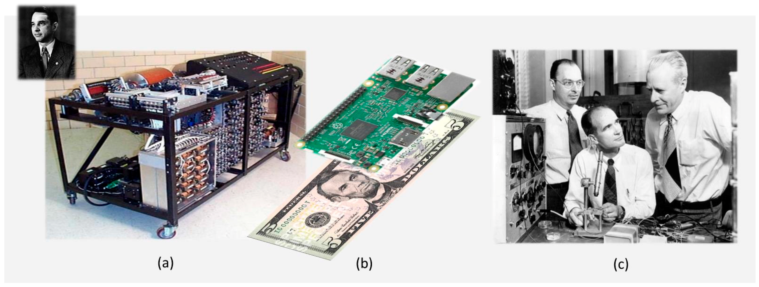
Figure 2.
The three major modes of heteroepitaxy: (a) the 2D layer-by-layer growth called Frank–Van der Merwe (FM) mode; (b) the 3D island growth called Volmer–Weber (VW) mode; and (c) the layer-plus-island growth called Stranski–Krastanov (SK) mode.
Figure 2.
The three major modes of heteroepitaxy: (a) the 2D layer-by-layer growth called Frank–Van der Merwe (FM) mode; (b) the 3D island growth called Volmer–Weber (VW) mode; and (c) the layer-plus-island growth called Stranski–Krastanov (SK) mode.

Figure 3.
Transmission electron microscopy (TEM) images of: (a) InGaN quantum dots [9] formed within a GaN structure and (b) AlGaN/AlN quantum wells [10], both within an AlN structure. (Reproduced from [9,10] with the permission of AIP Publishing).

Figure 4.
Top view of the epitaxial relationship between AlN (0001) and sapphire (0001) with 30° rotation with respect to each other. The distance marked as “a” is the separation between O2− atoms in sapphire [14]. (Reproduced from [14] with some modifications).

Figure 5.
Scanning electron microscopy (SEM) images of: (a) the patterned by e-beam lithography sapphire surface covered with ordered metallic aluminum mesas. The average sizes of the square mesas are 400 nm × 400 nm × 100 nm; (b) the pattern after low temperature annealing—the islands have converted into polycrystalline Al2O3; and (c) the pattern after the solid state crystalline conversion [19]. (Reproduced from [19] with the permission of J. Mat. Res.).
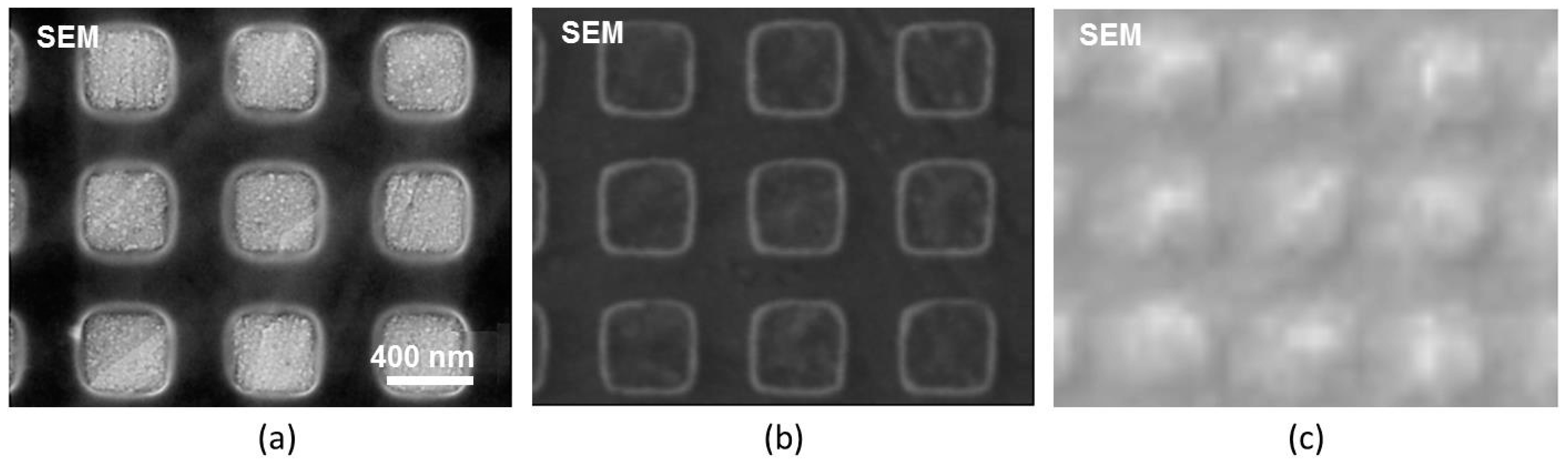
Figure 6.
(a) The normalized Light Emitting Diodes (LED) efficiency as a function of the dislocation density in some traditional III-V semiconductor compounds. [23] (Reproduced from [23] with the permission of AIP Publishing); (b) cross sectional view of a Nichia GaN/GaInN/GaN/Sapphire based LED [24] with dislocation density in the range of 1010/cm2. (Reproduced from [24] with the permission of Nature).
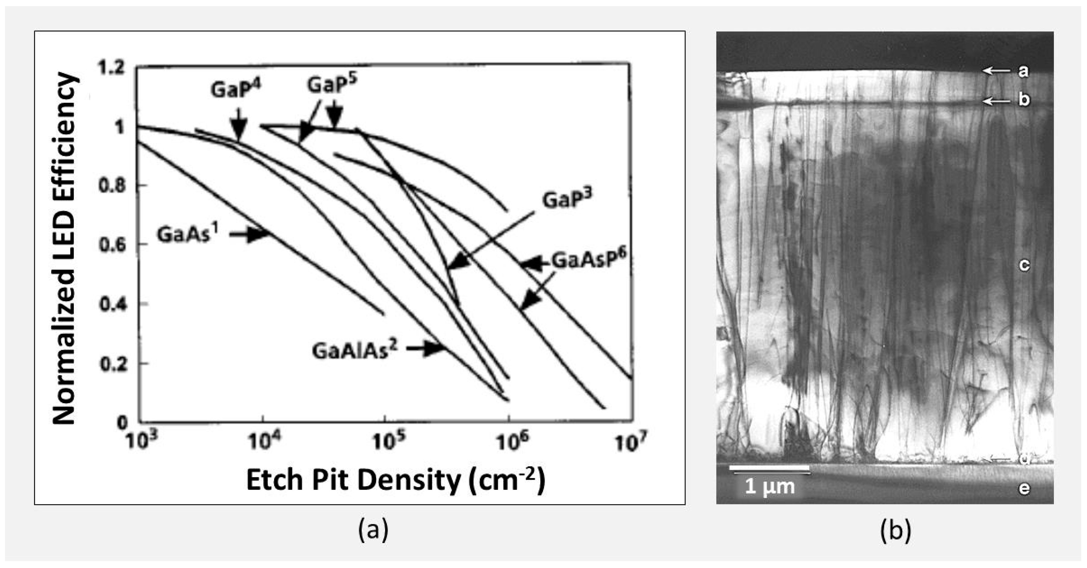
Figure 7.
(a) Different stages of an Epitaxial Lateral Overgrowth (ELO) growth—the front of crystallization may change or not its direction; (b) PENDEO epitaxy: the presence of a buffer layer is not necessary; in both cases blocking the vertical growth on the ridges may be purposely done by the deposition of a layer that prohibits the growth [31]. (Reproduced from [31] with the permission of J. Cryst. Growth).
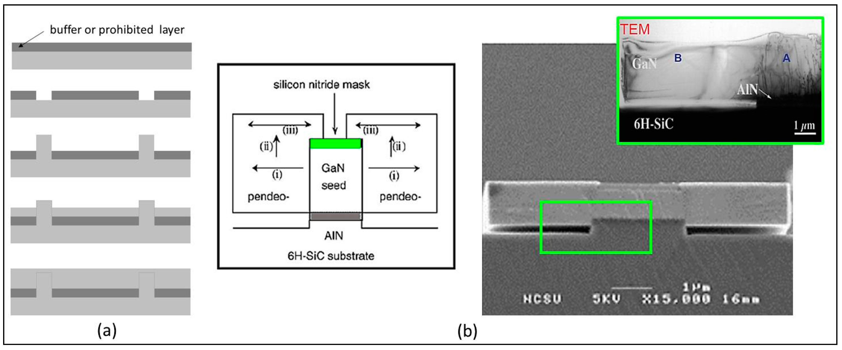
Figure 8.
(a) Theodore Maiman with the first Ruby laser demonstrated in 1960 at the Hughes Research Labs [37]; (b) Some of the available direct laser sources in the IR and THz region [38].

Figure 9.
(a) IR transparency of some traditional quasi-phase-matching (QPM) nonlinear optical materials [43]; (Reproduced from [43] with some modifications with the permission of SPIE); (b) A comparison of the two-photon absorption (2PA) coefficient β of GaAs and GaP in the near IR region between 1–1.7 µm. Initial measurements of 3PA in GaP (not shown here) indicate almost undetectably low numbers [44]. (Reproduced from [44] with some modifications with the permission of OSA).

Figure 10.
(a) The additional absorption band between 2–4 µm in GaP substrates (red line) does not exist in GaAs (green line) and is reduced in the Halide Vapor Phase Epitaxy (HVPE) heteroepitaxially grown GaP deposited on GaAs; (b) the HVPE grown material is as transparent in the IR as the commercial p-doped SI GaP [59]. (Reproduced from [59] with the permission of OSA).

Figure 11.
Nomarski microscope top layer surfaces of GaP grown on plain “on-axis” (100) GaP (a) and (100) GaAs (b) substrates. The samples are quarters of 2-inch wafers. The images are taken using stitching software at 2.5× magnification [59]. (Reproduced from [59] with the permission of OSA).
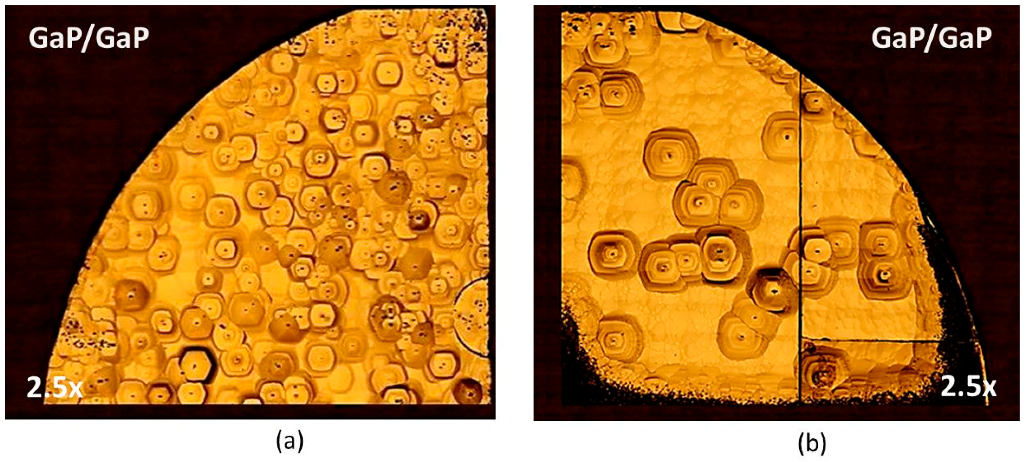
Figure 12.
(a) Due to poor parallelism 2 two-inch bonded “on-axis” (100) GaP wafers indicate a large useless area of voids between the wafers; (b) Such a problem does not exist when 2 GaAs wafers are bonded [59]. (Reproduced from [59] with the permission of OSA).
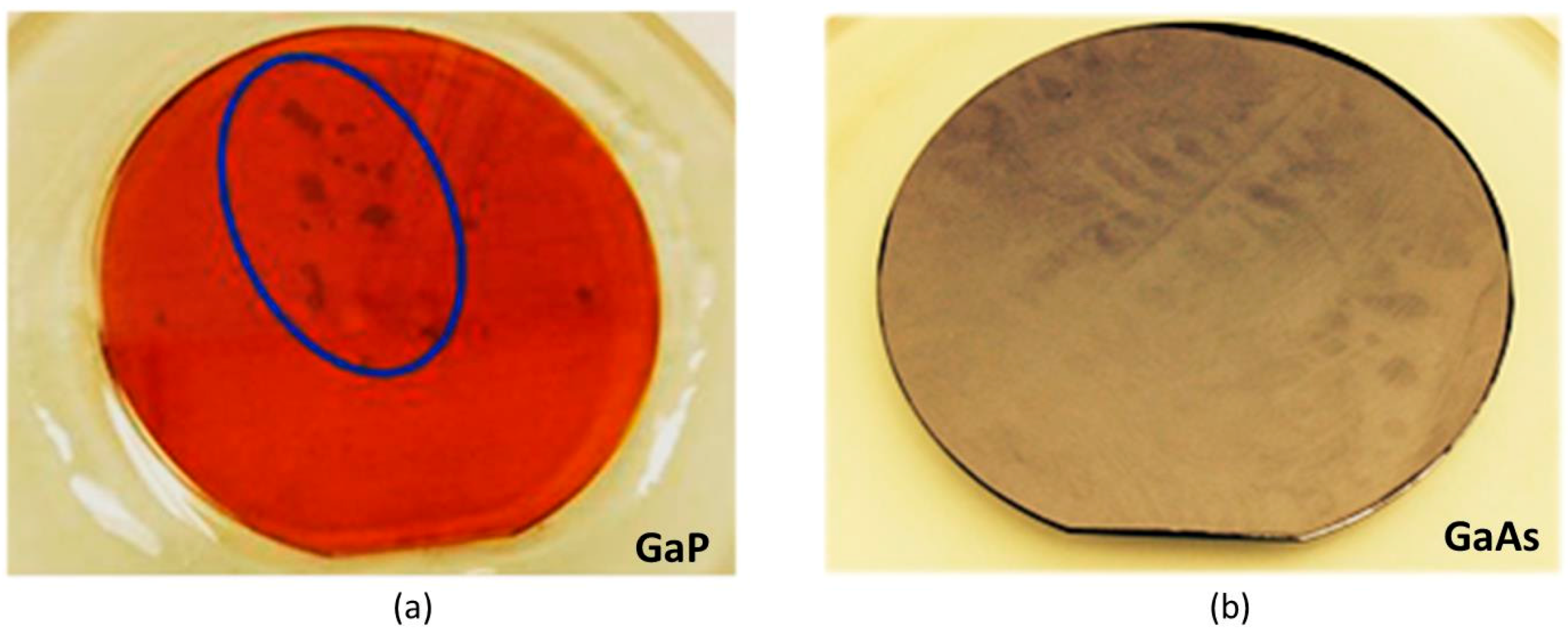
Figure 13.
(a) HVPE growth of GaP directly on Si; (b) Bandgap energy vs lattice constant for some of the most popular semiconductor materials (Reproduced from [65] with some modifications); (c) Physical vapor transport growth of OPZnSe on a OPGaAs template [64]. (Reproduced from [64] with the permission of J. Cryst. Growth).
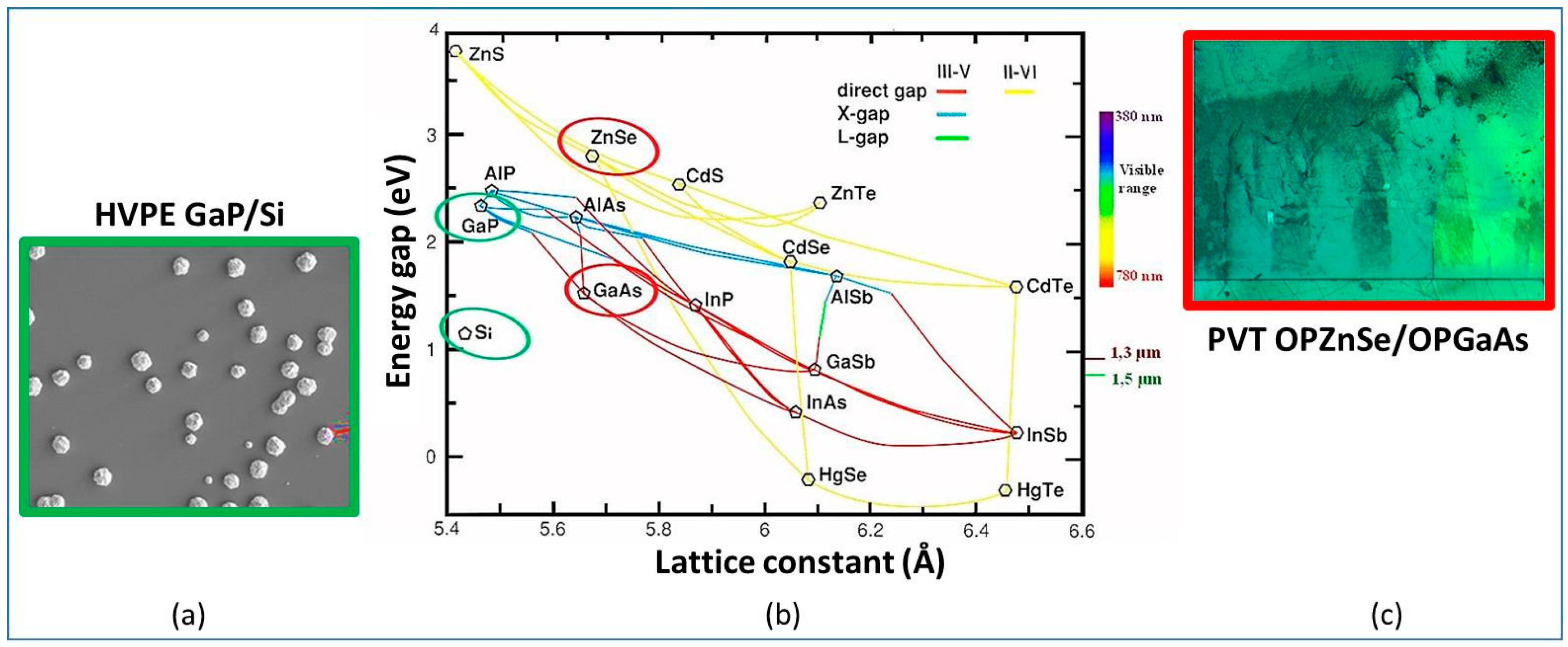
Figure 14.
(a) Atomic-force microscopy (AFM) images (1 µm × 1 µm square) of HVPE growth of GaP on GaAs show smooth surface morphology; (b) Full Width of Half Maximum (FWHM) omega-scan of GaP and GaAs substrate surfaces before growth and the related results after HVPE homo- and heteroepitaxy [59]. (Reproduced from [59] with the permission of OSA); (c) Reflection curves of omega-scans of a GaP and a GaAs substrate before the HVPE growth.
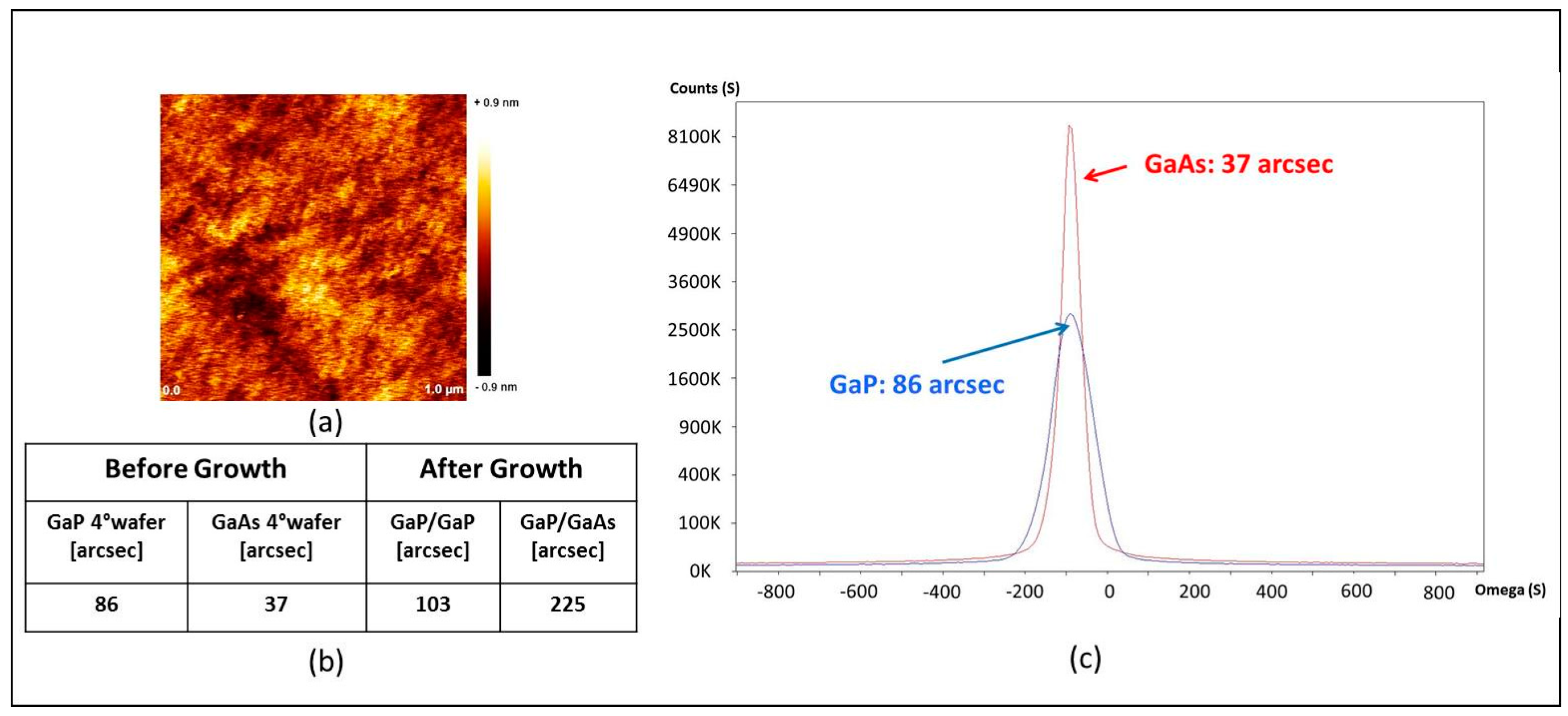
Figure 15.
(a) Cross section of HVPE heteroepitaxy of GaP on GaAs substrates; (b) Elemental profile analysis across the interface between the GaAs substrate and the grown GaP layer [59]. (Reproduced from [59] with the permission of OSA).

Figure 16.
(a) A cross section image of a combined HVPE growth, which starts first with a GaAs/GaAs homoepitaxy and after that continues with GaP/GaAs heteroepitaxy; (b) HVPE growth of GaAs03P0.66 on a GaP template.
Figure 16.
(a) A cross section image of a combined HVPE growth, which starts first with a GaAs/GaAs homoepitaxy and after that continues with GaP/GaAs heteroepitaxy; (b) HVPE growth of GaAs03P0.66 on a GaP template.
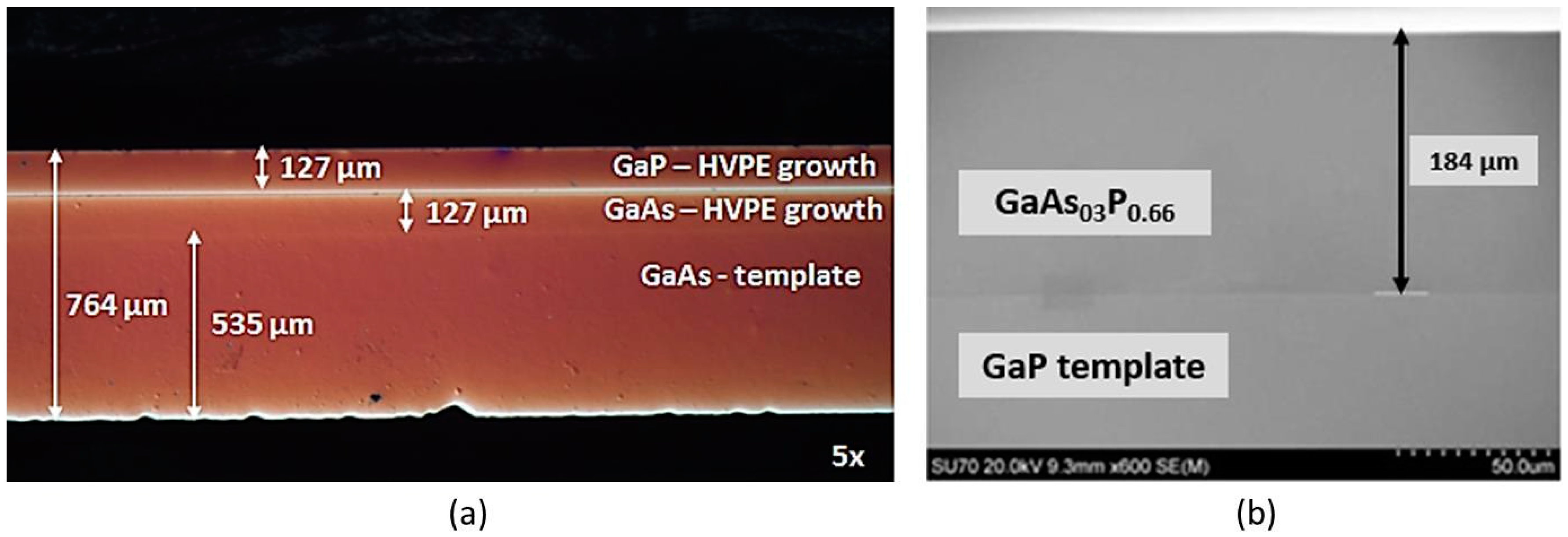
Figure 17.
(a) HVPE growth of GaP in a low-pressure horizontal quartz reactor; (b) parasitic nucleation on the quartz tube, luckily in the area that is behind the substrate [63]. (Reproduced from [63] with the permission of SPIE).
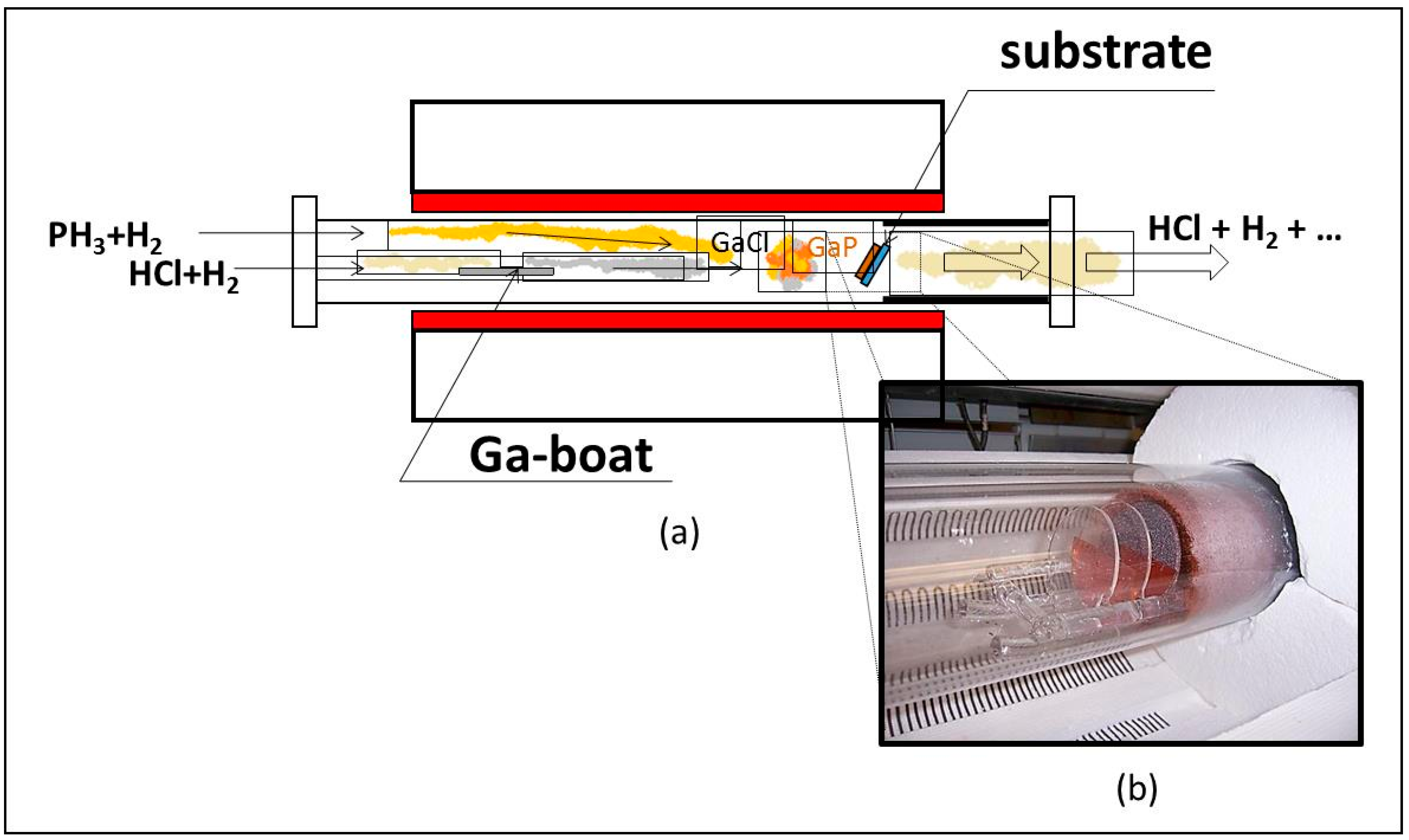
Figure 18.
Illustration of the most probable growth chemistry of GaP growing by HVPE in a low-pressure horizontal quartz reactor.
Figure 18.
Illustration of the most probable growth chemistry of GaP growing by HVPE in a low-pressure horizontal quartz reactor.

Figure 19.
(a) HVPE growth of GaP directly on Si (duplicates Figure 13a); (b) Nomarski top surface images of a direct homoepitaxial HVPE growth of GaP on a GaP substrate (upper image) and HVPE GaP grown on Metal Organic Chemical Vapor Deposition (MOCVD) GaP/Si; (c) SEM cross section of HVPE GaP grown on MOCVD GaP/Si.

Figure 20.
(a) Cross sectional images of GaN selective growth performed at different crystallographic directions and growth conditions [67] (Reproduced from [67] with some modifications); (b) Study selective growth of GaAs to determine the influence of growth temperature and V/III ratio on the mesas’ shape [68]. (Reproduced from [68] with the permission of J. Cryst. Growth).

Figure 21.
Zinc-blended structure of GaP with crystallographic orientations that provide opposite crystal polarities. The crystallographic planes of interest are outlined and shown separately. The right image shows a (100) GaP wafer with the standard directions of the major and minor flats.
Figure 21.
Zinc-blended structure of GaP with crystallographic orientations that provide opposite crystal polarities. The crystallographic planes of interest are outlined and shown separately. The right image shows a (100) GaP wafer with the standard directions of the major and minor flats.
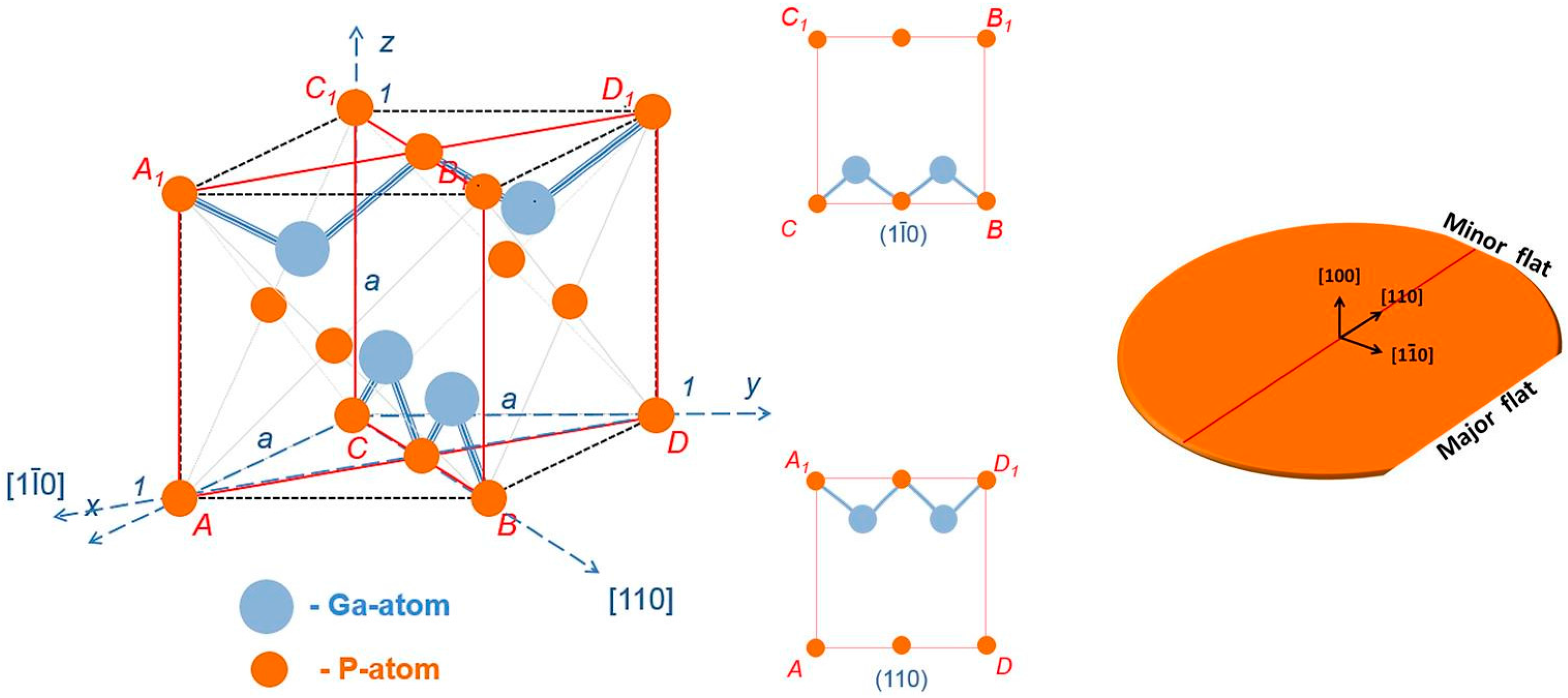
Figure 22.
(a) Two half-patterns deposited in two mutually perpendicular directions; and (b) cross section images of the layers grown on them [63]. (Reproduced from [63] with the permission of SPIE).
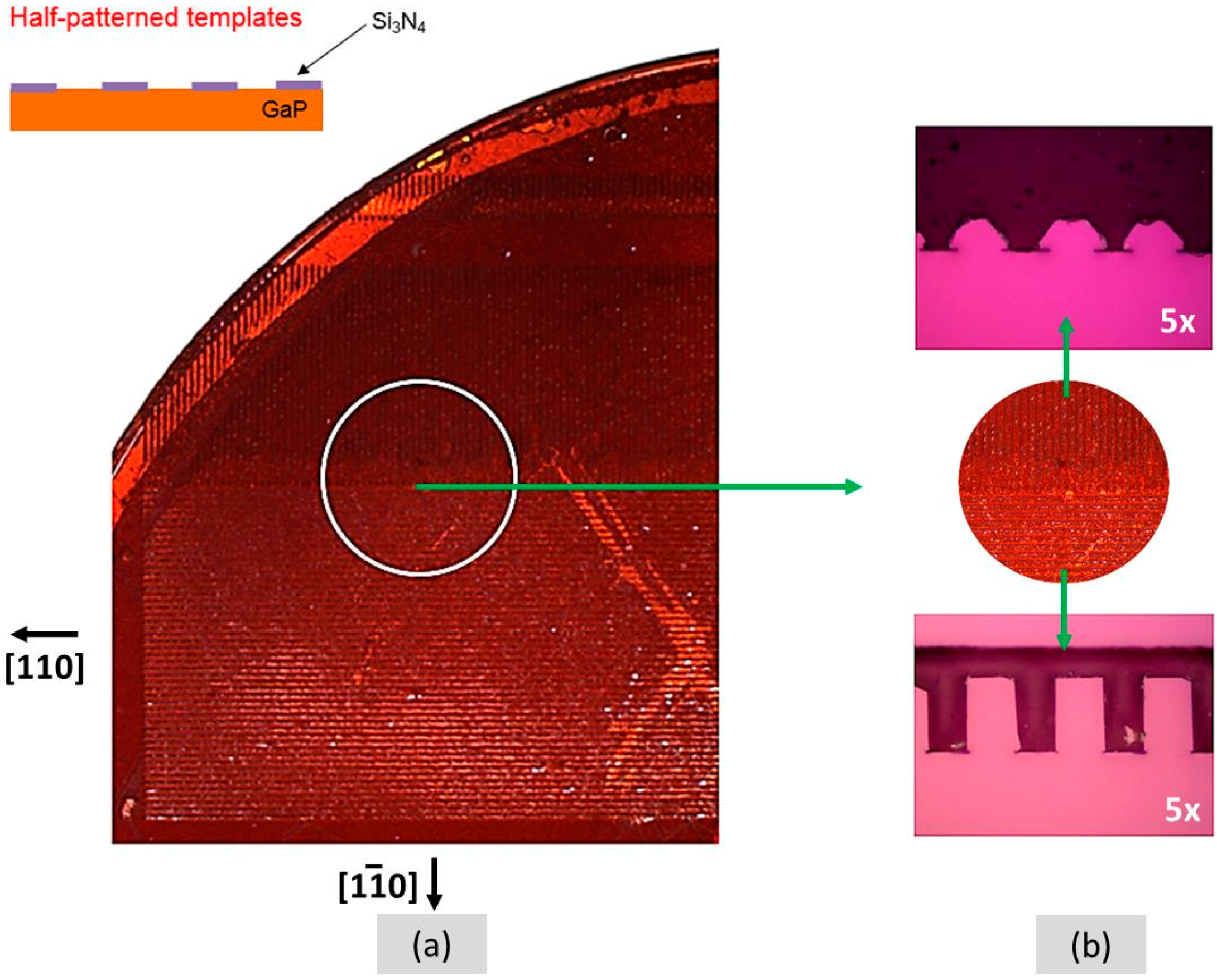
Figure 23.
(a) Growth on one “on-axes”, and (b) one misoriented with 4° towards [111]B (100) GaP wafer; (c) Six-hour thick HVPE growth on an HP-template with a pattern deposited along on a 4° misoriented towards [111]B (100) GaP wafer.
Figure 23.
(a) Growth on one “on-axes”, and (b) one misoriented with 4° towards [111]B (100) GaP wafer; (c) Six-hour thick HVPE growth on an HP-template with a pattern deposited along on a 4° misoriented towards [111]B (100) GaP wafer.

Figure 24.
First attempts on HVPE heteroepitaxy of OPGaP on OPGaAs templates at: (a) larger and (b) finer domain width. The left image is a 3D reconstruction showing the top surfaces of the layer before and after the growth and its cross section. The right image is a cross section of another layer grown at the same conditions on a pattern with finer periodicity [57]. (Reproduced from [57] with the permission of EOS).

Figure 25.
(a) One-hour homoepitaxial growth of OPGaP on OPGaP; (b) A four-hour homoepitaxial growth indicates that roughening of the layer surface and overgrowth of the pattern may occur at longer experimental times [63]. (Reproduced from [63] with the permission of SPIE).

Figure 26.
(a,b) State-of-the-art experiments limit the good domain propagation to up to 150 µm thick OPGaP layer homoepitaxially grown on OPGaP templates [69]. (Reproduced from [69] with the permission of SPIE).

Figure 27.
(a) The steps taken towards improvements of the OPGaP domain fidelity (2004–2007) preceded the following increase of the conversion efficiency; (b) The increase of the conversion efficiency from 16% to about 60% was achieved for a 5-year period (2004–2009) [63]. (Reproduced from [63] with the permission of SPIE).
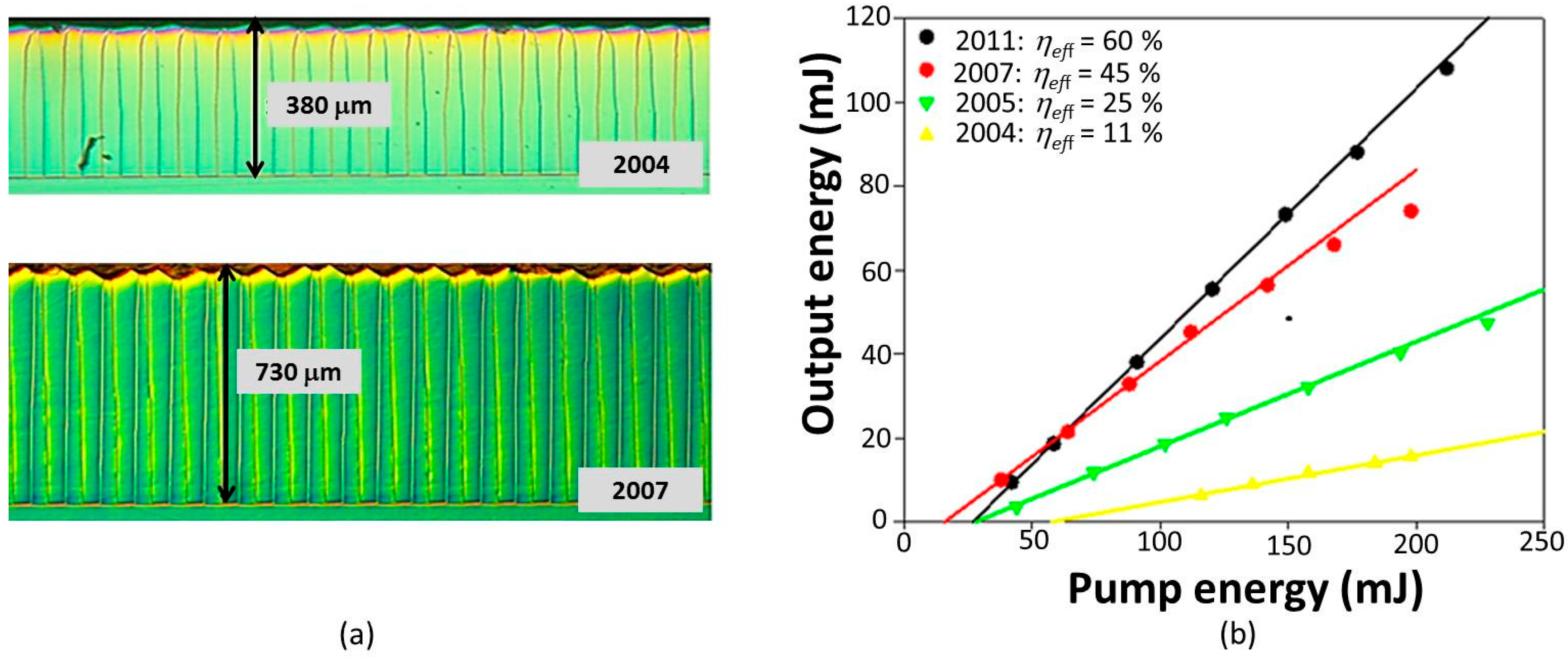
Figure 28.
(a) Frequency conversion in OPGaP at 3.54 µm pump beam [49]; (b) Homoepitaxial growth of OPGaP on a 3-inch OPGaP template—at finer pattern periods the pattern is often overgrown [50]. (Reproduced from [49,50] with the permission of SPIE).

Figure 29.
A 3D-reconstruction of heteroepitaxy of OPGaP on OPGaAs templates based on microscopic images that represent the top surface and the cross section—3 images in a row where the red arrows show where they must be stitched [59]. (Reproduced from [59] with the permission of OSA).

Figure 30.
Typical cross sections images of OPGaP grown by HVPE on Molecular Beam Epitaxy (MBE) assisted polarity inversion OPGaAs templates after: (a) 2–3 h of growth, and (b) 6–8 h of growth; (c) OPGaP grown by HVPE on wafer bonded OPGaAs templates [59]. (Reproduced from [59] with the permission of OSA).

Figure 31.
(a) Growth rate as a function of the duration of growth on bare substrates, as well on HP and OP templates; (b) Progress in the growth rate increase (2010–2013) with one eye on the influence of the growth rate on the layer roughness; (c) Growth rate as a function of the substrate temperature at two different V/III ratios [63]. (Reproduced from [63] with the permission of SPIE).

Figure 32.
Two pieces of grown OPGaAs: (a) before, and (b) after polishing off the triangular parts on the domain top surfaces; (c) two already faced against each other and aligned OPGaP pieces ready for high temperature bonding.
Figure 32.
Two pieces of grown OPGaAs: (a) before, and (b) after polishing off the triangular parts on the domain top surfaces; (c) two already faced against each other and aligned OPGaP pieces ready for high temperature bonding.

Figure 33.
Pseudomorphous growth in the case of heteroepitaxy of PbSe on PbS [4]. (Reproduced from [4] with some modifications with the permission of World Scientific).The small image of the lower right corner shows a TEM image of an area of the pseudomorphous growth during heteroepitaxy of GaP on GaAs [85]. (Reproduced from [85] with the permission of AIP Publishing).
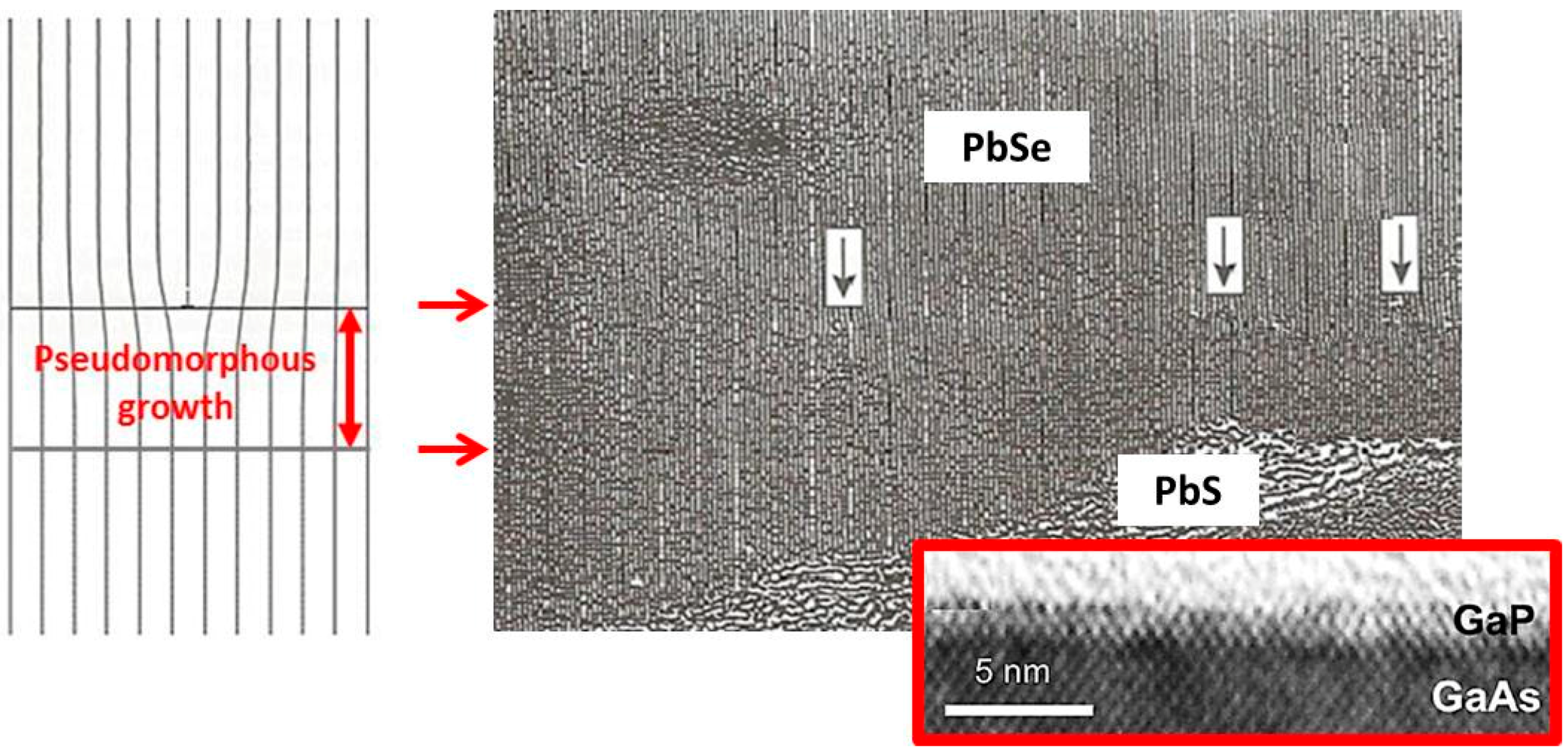
Figure 34.
Heteroepitaxy of OPGaP on OPGaAs templates. For simplicity the pseudomorphous growth is not presented on the image [4]. ((Reproduced from [4] with some modifications with the permission of World Scientific).
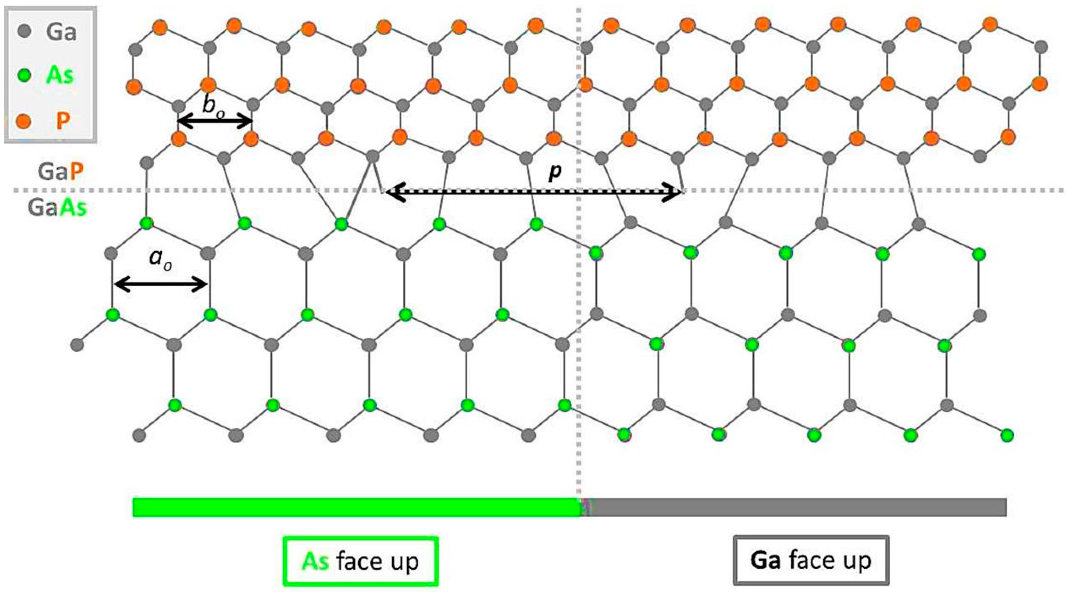
Figure 35.
(a) The zinc-blended GaP structure. The crystallographic plane of interest ADC1 is outlined; (b) conducting the tensile biaxial strain σ during GaP/GaAs heteroepitaxy [85]. (Reproduced from [85] with the permission of AIP Publishing).
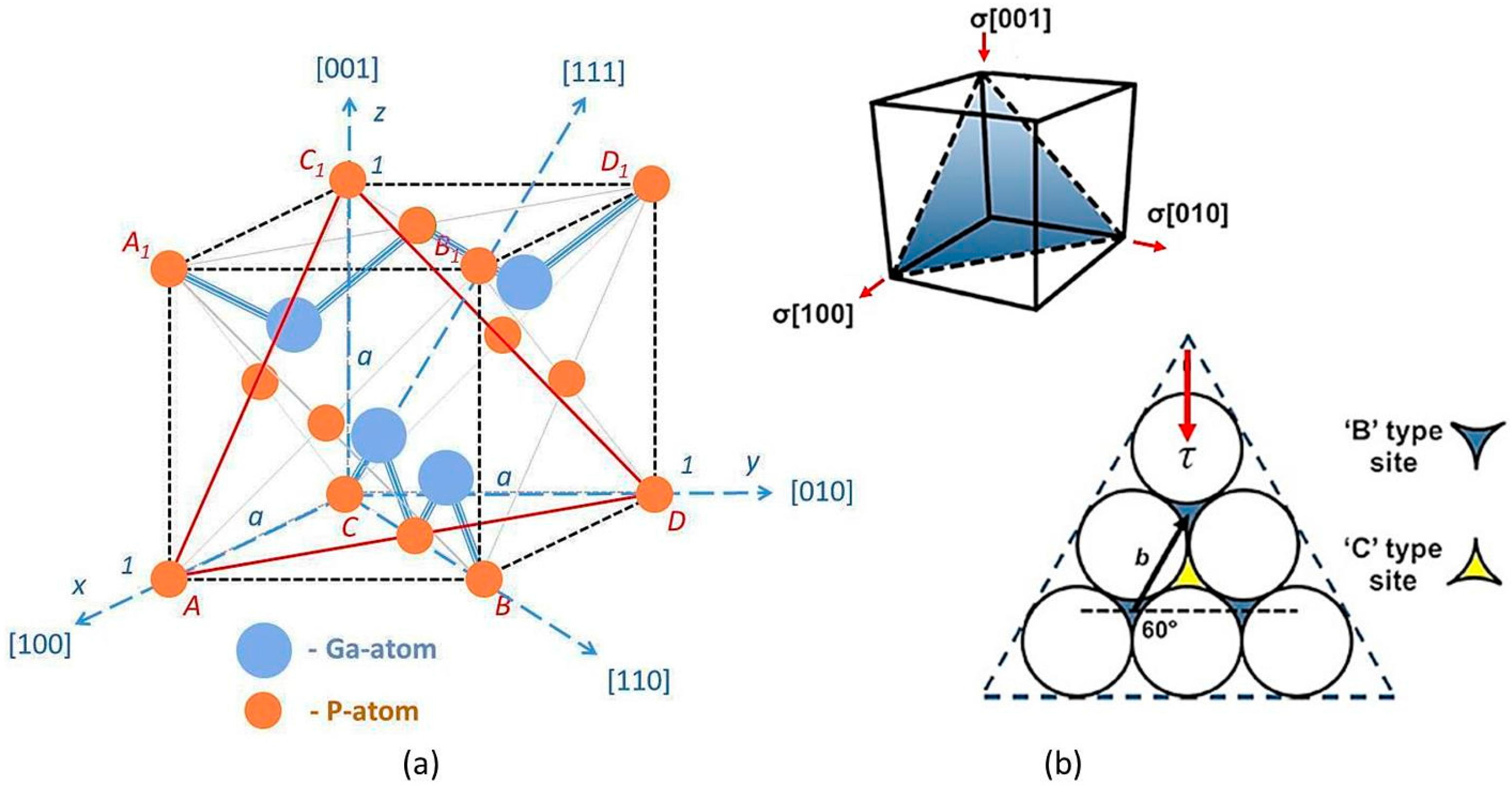
Figure 36.
(a) Formation of 30° and 90° Shockley partial dislocations; (b) a TEM image of the two partials bonded by a narrow stacking-fault “ribbon” [85]. (Reproduced from [85] with the permission of AIP Publishing).

Figure 37.
(a–d) TEM cross section images with different magnification in the area near to the GaP/GaAs interface; (e) a cross section image of a thick HVPE grown GaN layer that shows a reduction of the dislocation density with layer thickness [96]. (Reproduced from [96] with the permission of AIP Publishing); (f) top surface of thick HVPE grown GaP on GaAs substrate showing smooth surface morphology.
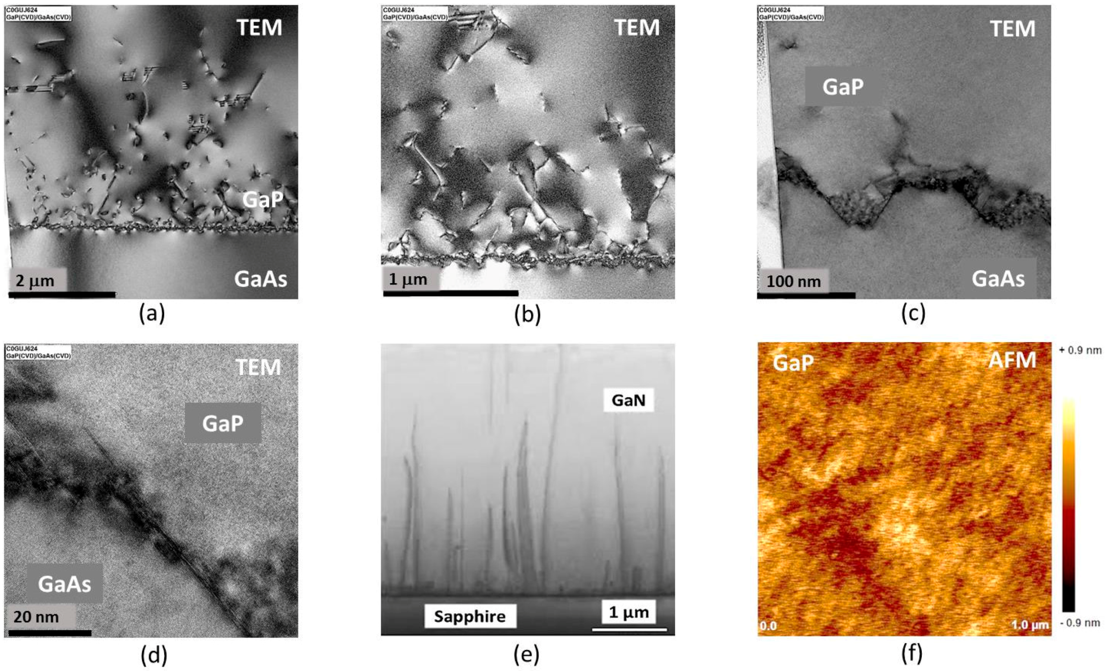

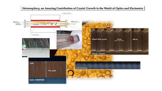
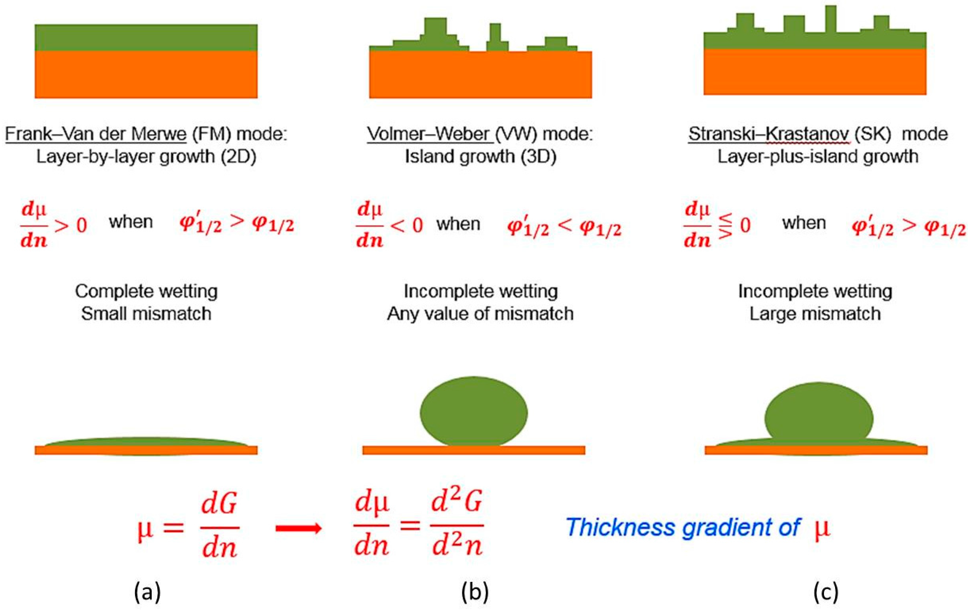
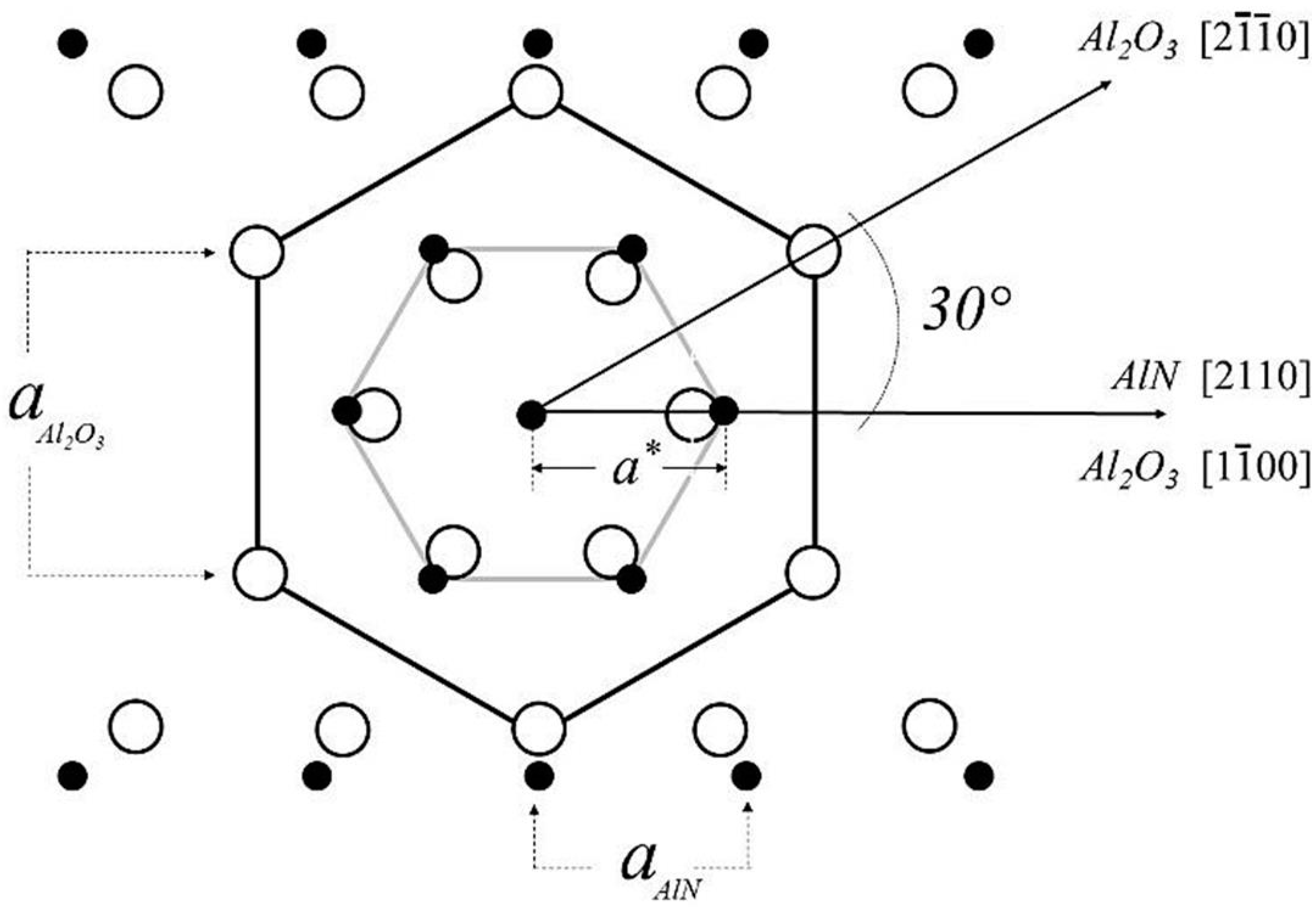
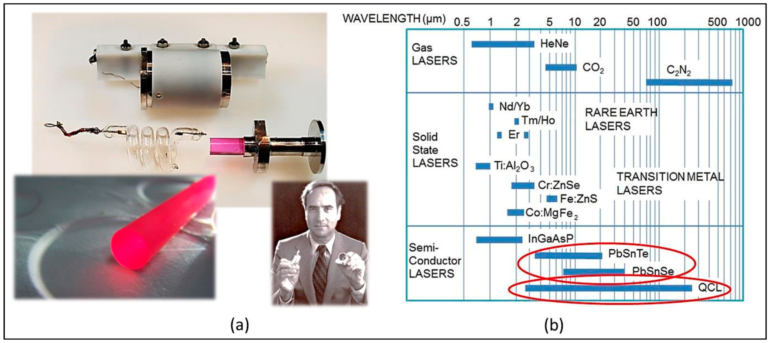
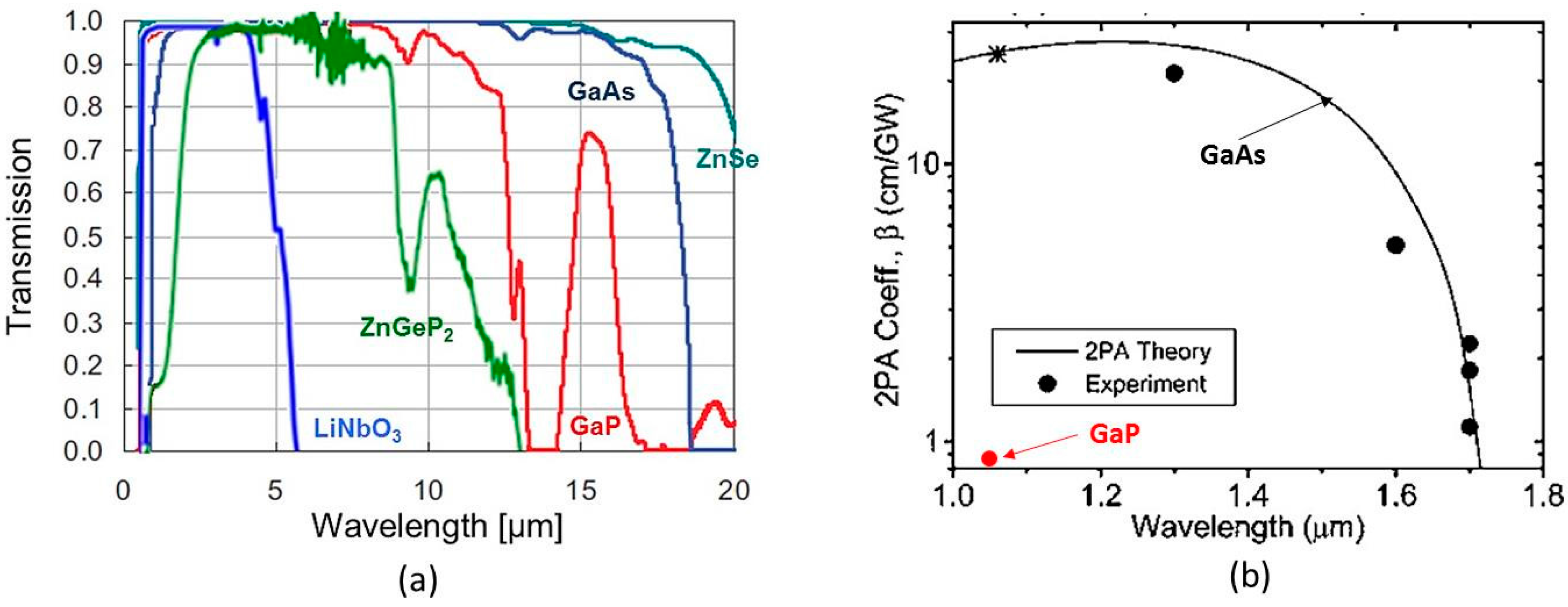
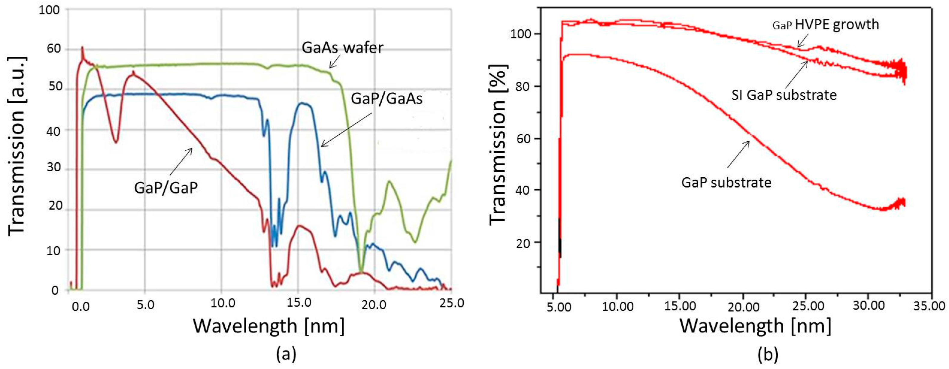
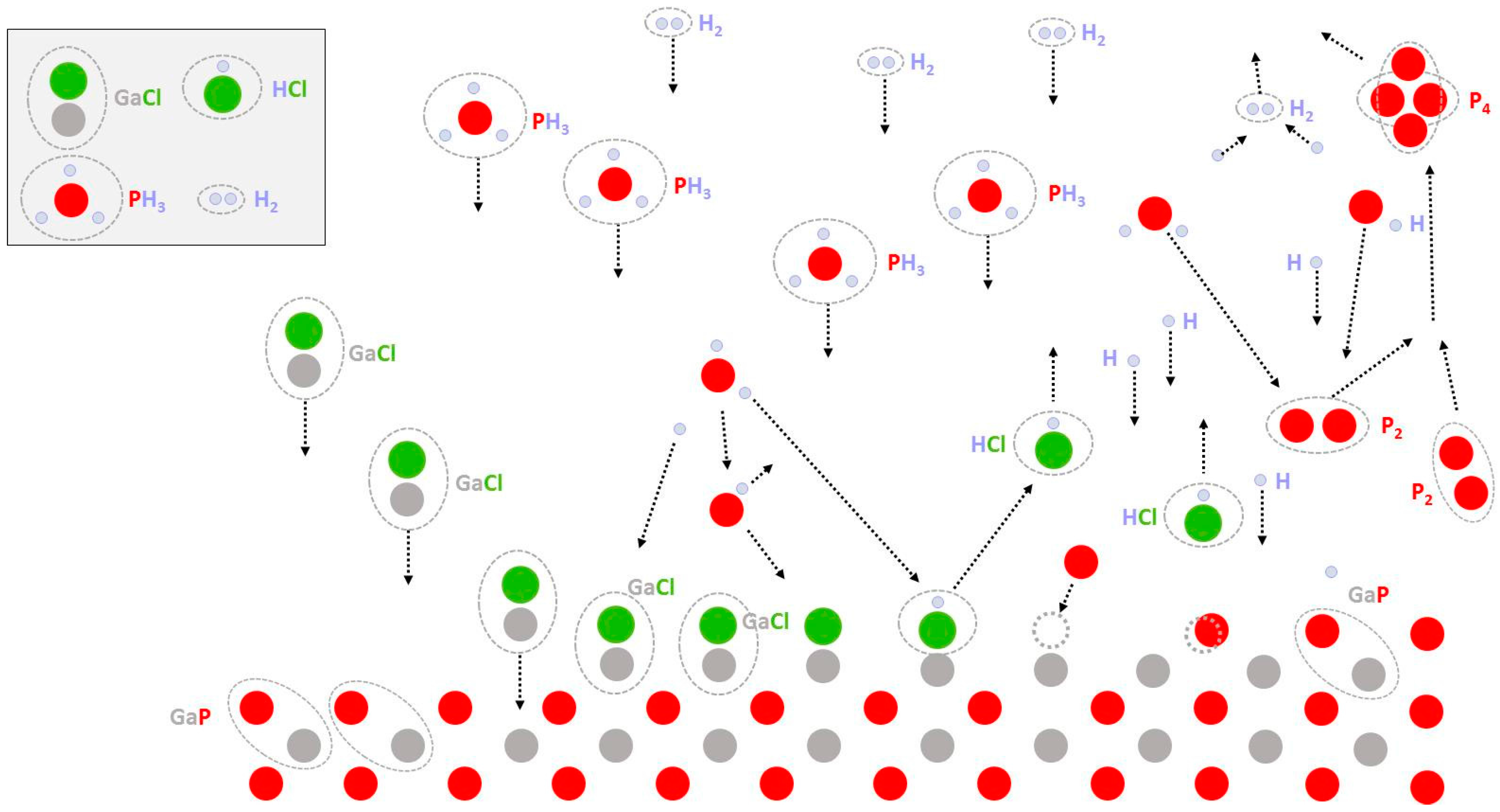
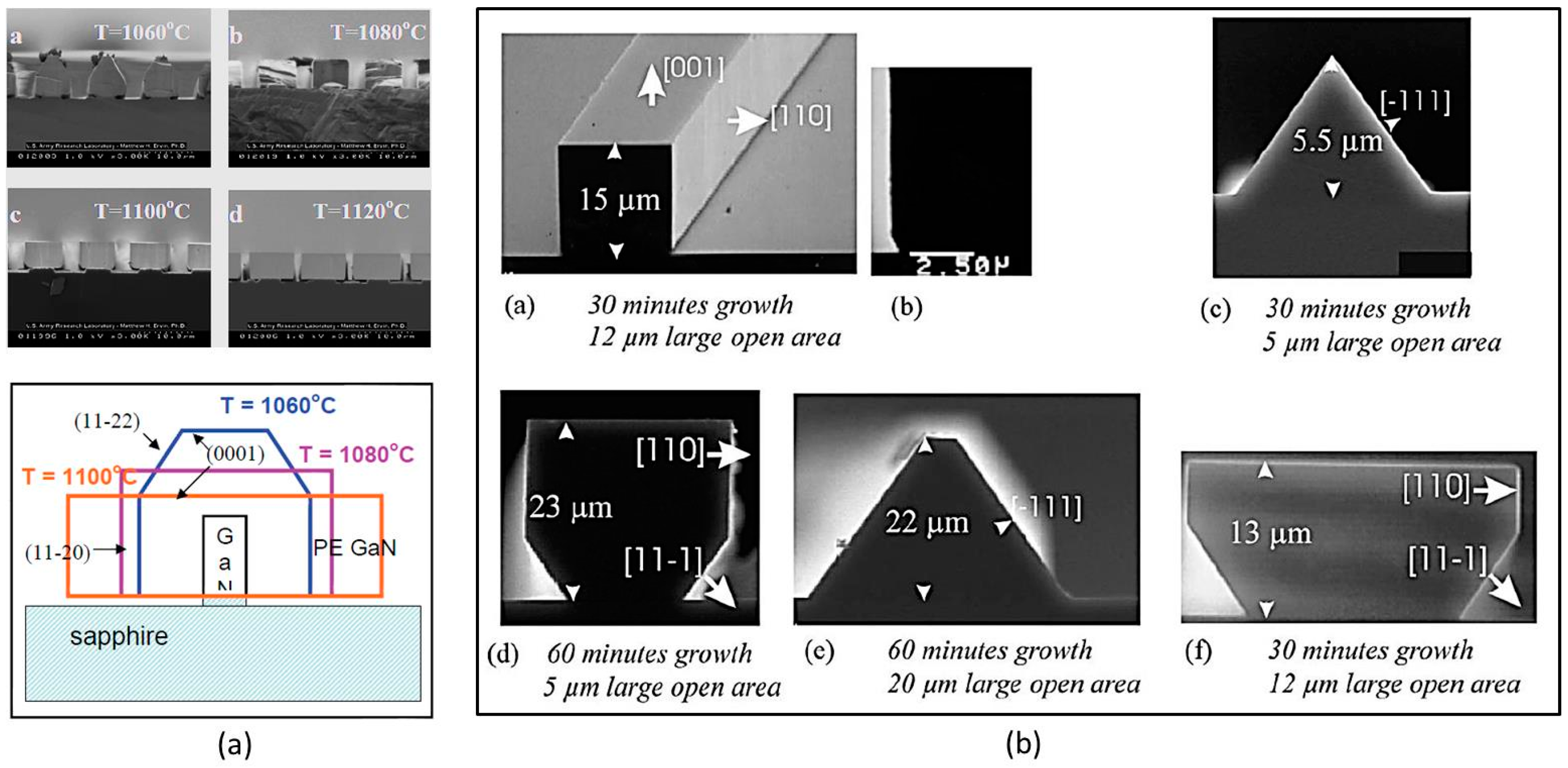
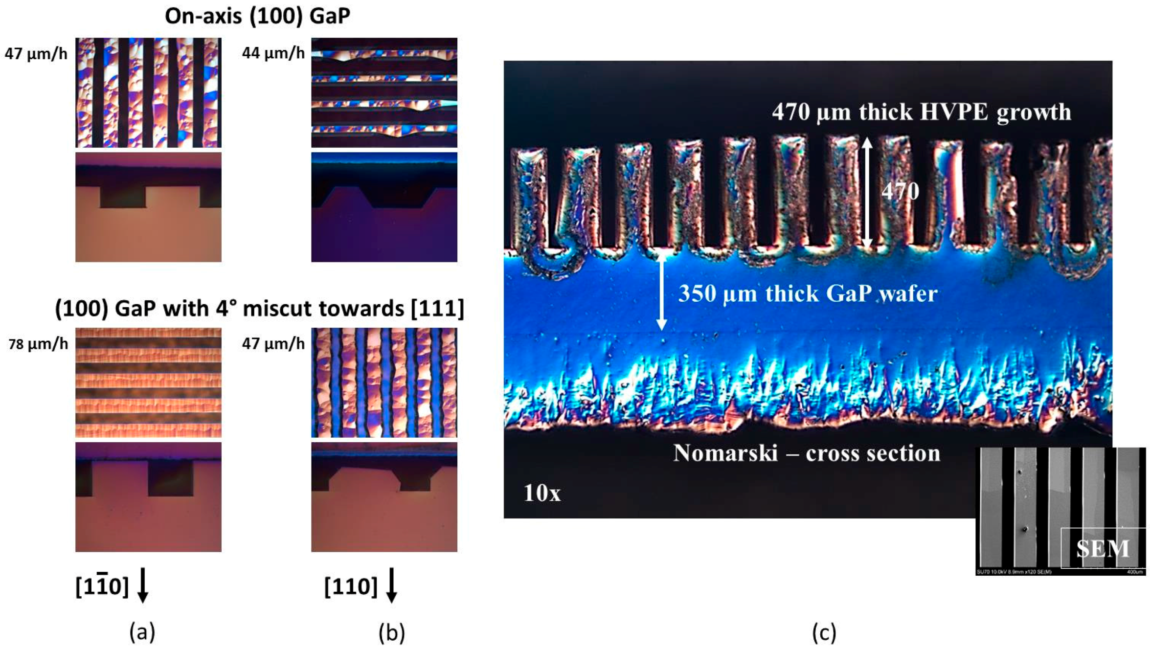
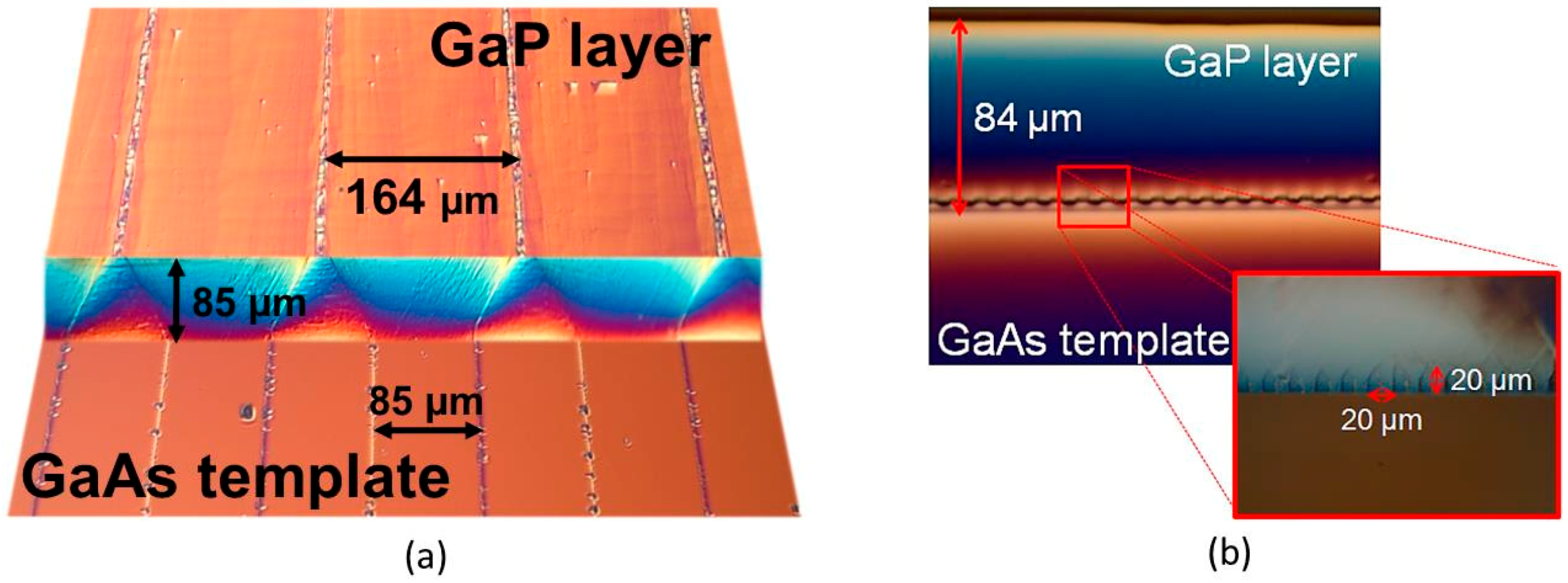
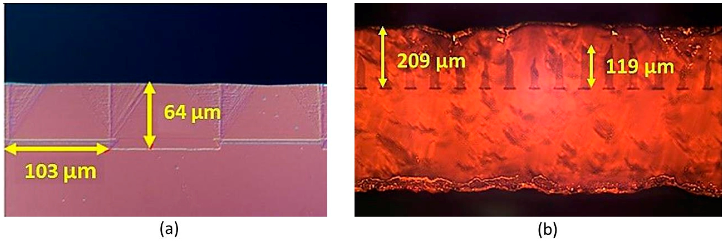
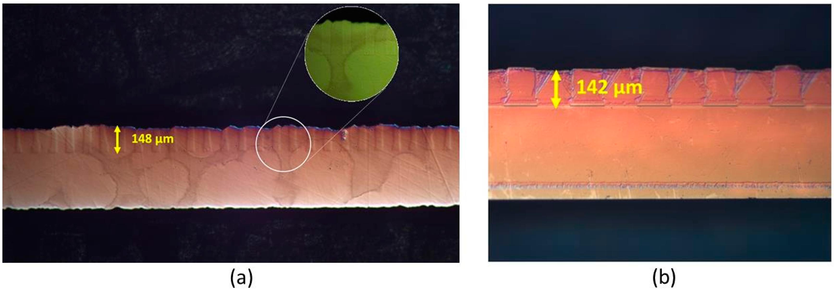
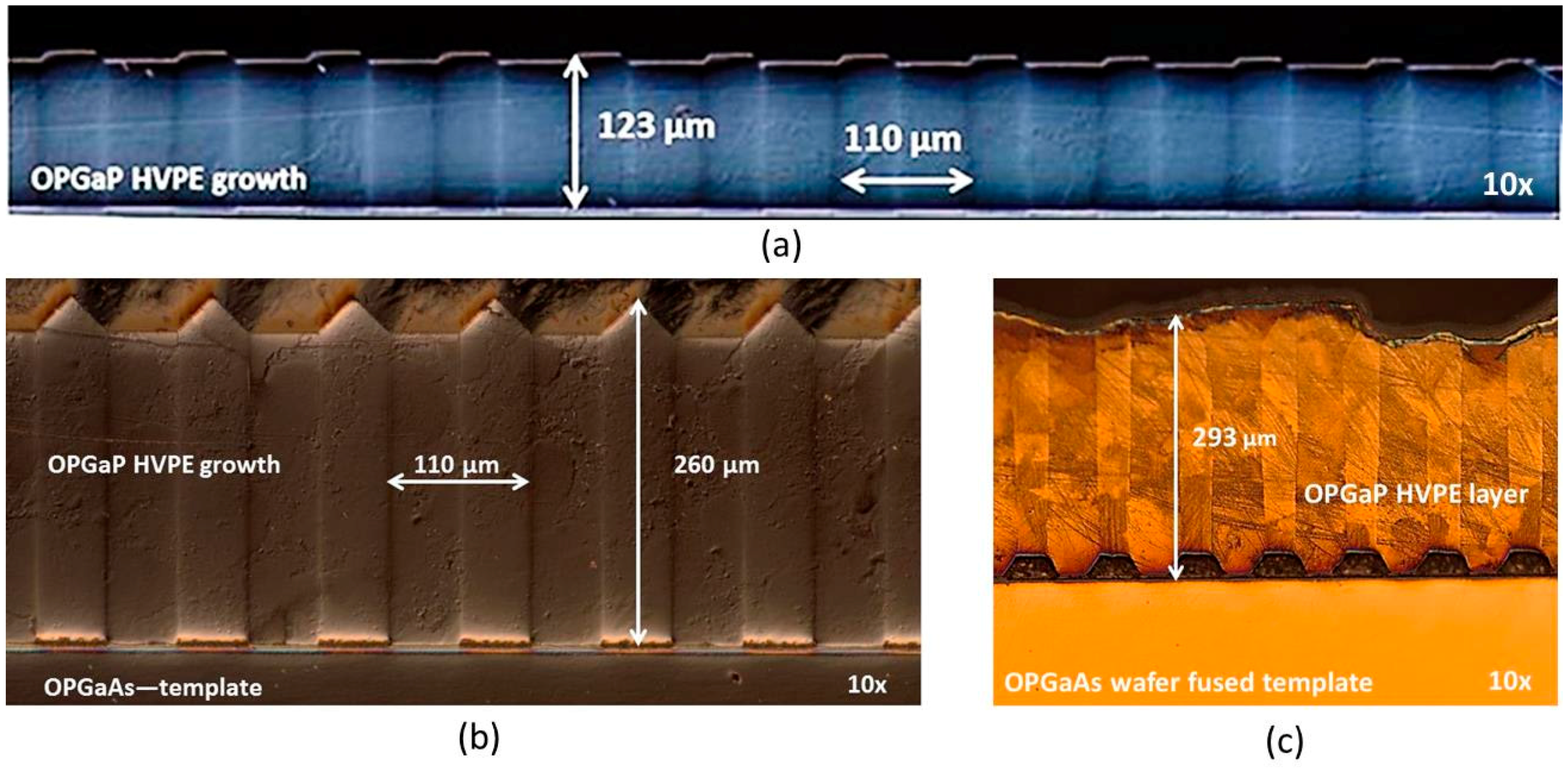
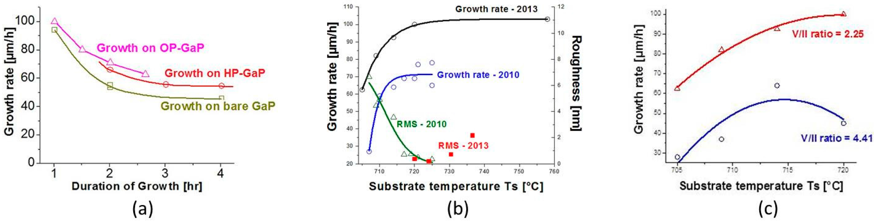
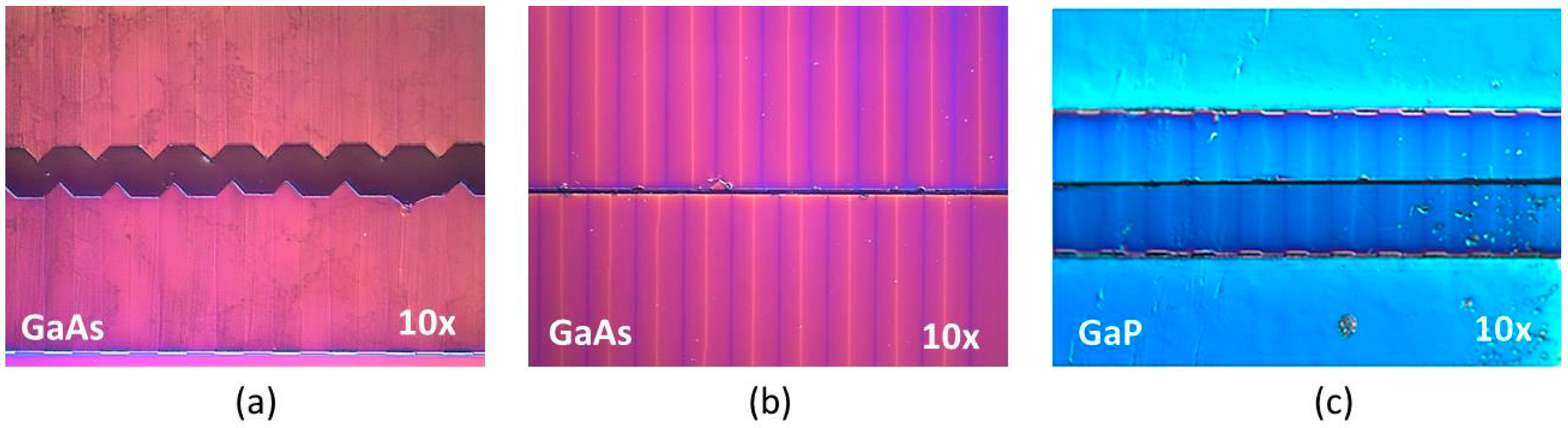
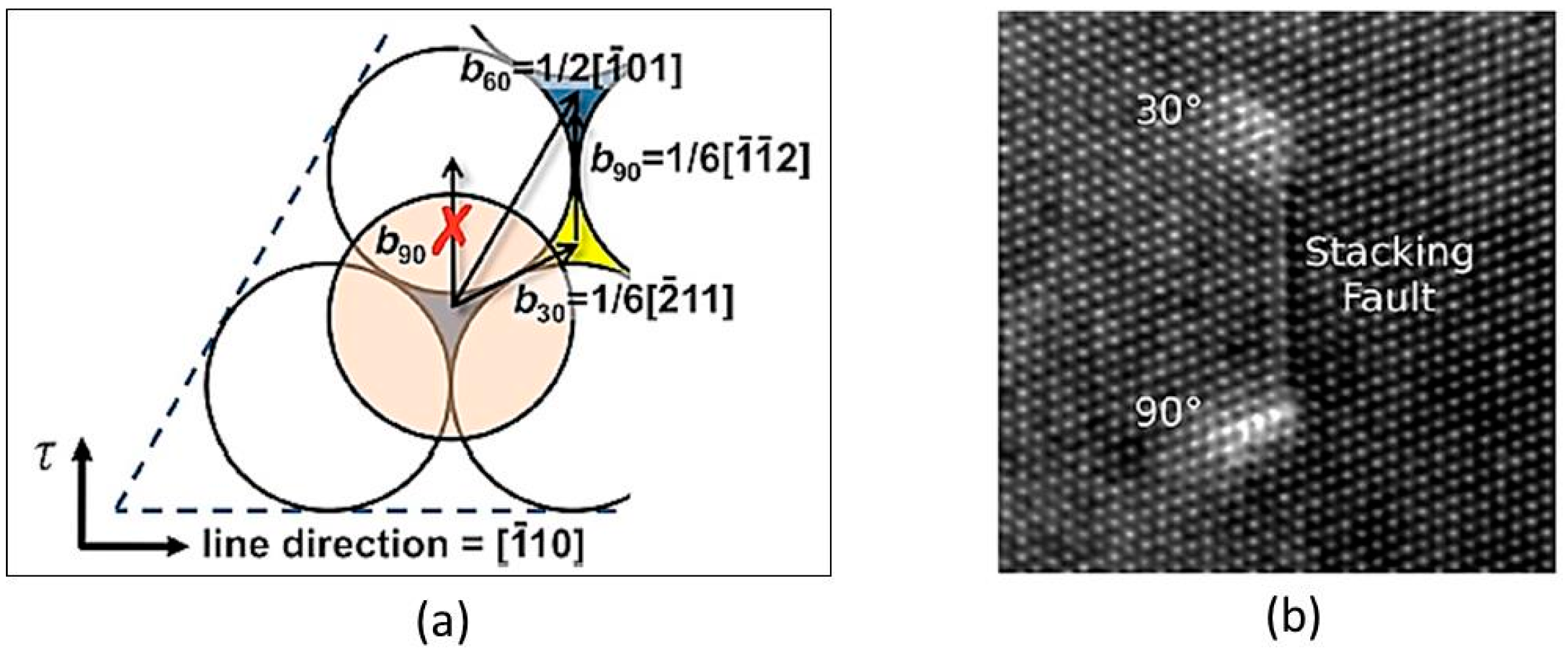
Table 1.
A comparison between some optical and thermal properties of GaAs and GaP. 2PA = two-photon absorption.
Table 1.
A comparison between some optical and thermal properties of GaAs and GaP. 2PA = two-photon absorption.
| Properties | GaAs | GaP |
|---|---|---|
| Transmission window [μm] | 1–16 | 0.55–12 |
| Nonlinear optical coefficient d14 [pm·V−1] | 94 | 71 |
| Index of refraction n | 3.34 | 3.03 |
| Thermal conductivity [W·m−1·K−1] | 55 | 110 |
| Thermal expansion coefficient [10−6·K−1] | 5.7 | 4.6 |
| 2PA coefficient [cm/G−1·W−1] at 1.06 μm | 28 | 0.02 |
Table 2.
A comparison of price and quality (EPD/cm2) of commercial 2-inch GaP and GaAs wafers.
| Characteristics/Wafer Material | GaP | GaAs |
|---|---|---|
| Price [USD] | 585–685 | 87–90 |
| EPD [etch pits/cm2] | 80,000–100,000 | 1500–5000 1 |
1 The data represent the ranges for price and EPD taken from several recent vendors’ quotes.
© 2017 by the author. Licensee MDPI, Basel, Switzerland. This article is an open access article distributed under the terms and conditions of the Creative Commons Attribution (CC BY) license (http://creativecommons.org/licenses/by/4.0/).
Share and Cite
MDPI and ACS Style
Tassev, V.L. Heteroepitaxy, an Amazing Contribution of Crystal Growth to the World of Optics and Electronics. Crystals 2017, 7, 178. https://doi.org/10.3390/cryst7060178
AMA Style
Tassev VL. Heteroepitaxy, an Amazing Contribution of Crystal Growth to the World of Optics and Electronics. Crystals. 2017; 7(6):178. https://doi.org/10.3390/cryst7060178
Chicago/Turabian StyleTassev, Vladimir L. 2017. "Heteroepitaxy, an Amazing Contribution of Crystal Growth to the World of Optics and Electronics" Crystals 7, no. 6: 178. https://doi.org/10.3390/cryst7060178
Note that from the first issue of 2016, this journal uses article numbers instead of page numbers. See further details here.