1. Introduction
Liquid crystal (LC) plays an important role on modulating light properties such as intensity, phase and polarization. Many LC devices are invented for various optical applications, such as LC displays for light intensity control [
1], LC Spatial Light Modulator (SLM) for spatial phase modulation [
2,
3], and Q-plate for controlling orbital angular momentum of photons [
4,
5]. For all these LC devices, it is critical important to precisely control the LC molecule director distribution. There are majorly two techniques for controlling the LC molecule director distribution. The first technique is spatially electric field control via patterned electrode [
1], which is the most common used technique for various LC devices such LC displays and SLM. The second technique is surface alignment control via special treatment on the surface alignment material, such as rubbing of polyimide [
6], photoalignment [
7], and silicon oxide evaporation [
8]. Among various alignment methods, the photoalignment technology has been drawing increasing attention for its good alignment quality and ability to avoid the problems caused by traditional rubbing technology such as generation of contaminating impurities and electrostatic charges and giving damages to alignment layer [
7]. More importantly for light modulation, it is convenient for the photoalignment technology to achieve patterned alignment structure by exposing different areas with light in different polarizations, propagation directions or intensities. In this way, a customized LC director distribution can be achieved to offer special designed optical functions. Many photonic devices can be achieved via patterned alignment, including patterned retarders [
9,
10], Q-plates [
4,
5], LC gratings [
11,
12], LC lenses [
13,
14,
15], and polarization converters [
16,
17,
18], etc., which could find many important applications in beam shaping [
4], imaging system [
13,
14], Complementary Metal Oxide Semiconductor (CMOS) sensor system [
19] and 3D display [
10], etc.
Among the various kinds of photonic devices, we are particular interested in this paper to apply the patterned photoalignment technology on an important photonic device called dammann grating (DG). The Dammann grating is a kind of specially designed binary phase (0, π) grating that could create a diffraction pattern where the intensities of the diffracted spots are equal in some orders [
20,
21]. The idea of these kinds of grating was first proposed by Dammann and Gortler in 1971 to obtain multiple images from one input object for optical lithography [
21]. Later on, the DGs have been proposed for using in lots of interesting application, such as laser beam summation [
22], optical interconnections [
23], three-dimensional (3D) optical imaging [
24], 3D lattice structures generation [
25], and optical communication [
26]. Moreover, by modifying the grating structure, the optical function of the DG is also extended to be more versatile such as the generation of array of diffractive orders with different vortex phase distribution [
26,
27]. To fabricate the DG, the conventional used method is the Very-large-scale integration (VSLI) technology, which forms by the steps like preparing mask using electron beam or laser and etching substrate with plasma, reactive ion or wet chemical [
28]. The advantage of this fabrication method is high resolution up to sub-micrometers, but the disadvantage is that the grating is fixed with no tunability and the fabrication process is tedious and complicated.
Recently, more and more DGs are produced based on LC devices [
25,
27,
29,
30], which are either based on patterned electrode [
25] or patterned photoalignment technology [
27,
29,
30]. Comparing with the LC DGs based on patterned electrode, the ones based on patterned photoalignment show advantage on its simple fabrication process, cheap cost and high structure resolution down to sub-micrometer level [
31]. The most important property and advantage of the LC DG is that the grating is electrically tunable, which offers great potential to benefit lots of optical applications such as optical communication and beam shaping. Moreover, the working principle of LC DG is unique since it uses the geometric phase [
15] instead of the conventional dynamic phase which is controlled by optical path difference. For the LC DG, the electrically switching speed is critical important which plays key role in optical applications. To improve the switching speed, different kinds of LC materials are used such as dual-frequency LC [
30] and blue phase LC [
27], both with relative fast switching time in the range of ms level. However, both of these two kinds of devices require strict operation conditions, such as the complicated driving scheme for dual-frequency LC and ultra-high driving voltage (~180 V) for blue phase LC.
To further increase the switching speed, we propose to apply the ferroelectric liquid crystal material for building the DG. FLC is considered to be a good candidate for modern display and photonics applications [
32,
33], which shows nearly the fastest switching speed among all the LC materials. In this paper, a faster switching FLC DG based on patterned photoalignment is demonstrated. The switching speed of the FLC DG can go down to several tens of us which are at least one order faster than other LC DGs. Meanwhile, the FLC DG only requires low driving voltage (10 V) and very simple operation conditions, which overcomes the drawbacks of dual-frequency LC and blue phase LC devices.
2. Results
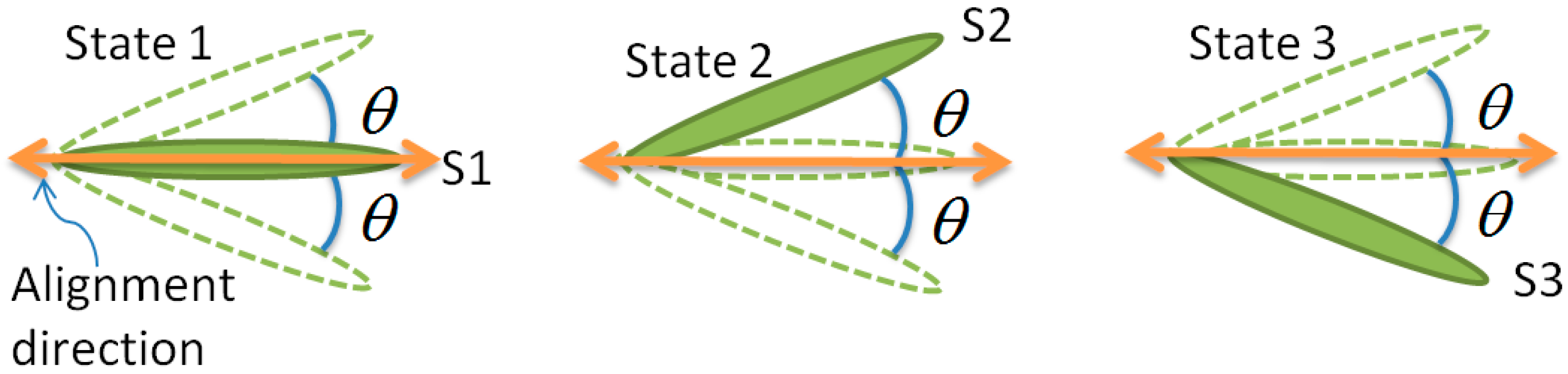
In this paper, the used FLC materials is working in a electro-optical mode called electrically suppressed helix (ESH) mode, which is characterized by the good alignment quality and faster response time at low driving voltages [
32,
33]. The working principle of the ESH FLC can be illustrated by
Figure 1. For the structure of a typical ESH FLC device, the FLC material is sandwiched between two ITO glass substrates on top of which alignment layer is coated and aligned. Normally when no voltage is applied on the FLC cell, the FLC helix will be aligned along the alignment direction (S1) and the molecules will rotate with smectic helical structure, represented by state 1 in
Figure 1. When an electric field (>0.5 V/μm) is applied on the FLC cell, the helical structure will be suppressed and the FLC molecules will switch to either side of the position parallel to the substrates around the cone surface, shown as state 2 and 3 in
Figure 1. The different switching states 2 and 3 are decided by the polarity of the electric field applied on the FLC cell. In state 2 and 3, the FLC molecule will be aligned along the S2 and S3 axis, which can also be considered as the slow optical axis of the FLC based wave-plate. The angle θ is called tilt angle which is determined by the material itself. In the FLC DG, the FLC material FD4004N is used and its tilt angle θ ≈ 22.05°.
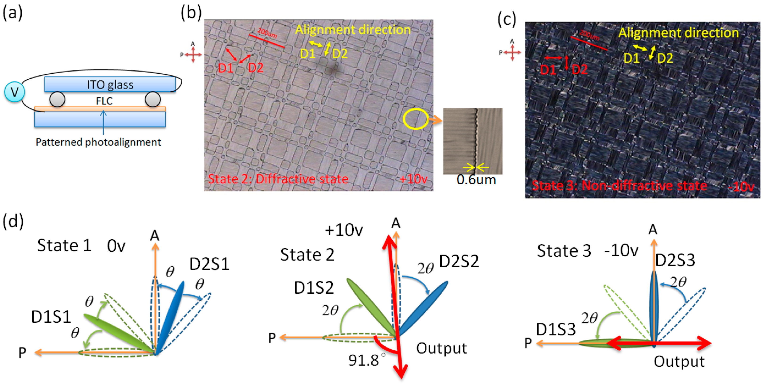
The structure of the prepared FLC DG is shown in
Figure 2a, in which a patterned photoalignment layer with special designed DG structure is produced in one substrate. In the prepared FLC DG, the FLC molecules are working in either state 2 or 3 as the diffractive state or non-diffractive state.
Figure 2b,c show the micrograph of the prepared FLC DG in states 2 and 3 under crossed polarizer (P) and analyzer (a). In the lower right corner of
Figure 2b, the border area between two domains is zoomed and a transition line can be observed. According to the measurement, the transition line width is around 0.6 μm. In the FLC DG, there are two orthogonal aligned domains (D1 for domain 1, D2 for domain 2), as marked using yellow arrows in
Figure 2b,c.
Figure 2d illustrates the molecule orientation in different states for the two domains. In state 1, the FLC molecule in both domains is aligned along the alignment direction with smectic helical structure, shown as D1S1 for domain 1 state 1 and D2S1 for domain 2 state 1. In states 2 and 3, different polarity of electric field with amplitude fixed to 10 v is applied in the LC cell, the molecule orientation is switched to D1S2 and D2S2 for the two domains in state 2, and D1S3 and D2S3 for the two domains in state 3. It can be seen that in both states 2 and 3, the molecule orientation is kept orthogonal for the two domains. The switching between these two states is an overall rotation of molecule orientation for an angle 2θ ≈ 44.1°. We can also observe from the microscopic figures for State 2 and 3, that the FLC textures still exist which results some lines within each domains and the border between two domains is not so straight, as shown in
Figure 2b. The above mentioned phenomenon may influence the optical performance of the device, such as the scattering, efficiency or uniformity of the device. To optimize the performance of the device, certain effort may be needed to optimize the parameters of the FLC materials, which is out of the scope of this paper.
In states 2 and 3, all neighbored domains have orientations in orthogonal direction. All polarized light passes through the DG can be decomposed to two orthogonal directions along the two molecule orientation directions. In both the two polarizations, the light will observe the same phase difference between any of the two neighbored domains, which can be controlled by varying the FLC cell thickness. In our case, the phase difference between neighbored domains is optimized to be close to
to make sure the best performance of the FLC DG. Since for both the two polarizations, the phase difference all follows the well-designed domain structure, the diffractive performance of the DG can be considered as polarization-independent for both states. The LC device structure with orthogonal oriented LC molecule and π phase difference between neighbored domains is commonly used for realizing lots of other optical elements such as Fresnel plate [
34] and grating [
35]. In our design, the switchability of the device is critical important. To achieve the electrical switchability, a polarizer (P) and an analyzer (a) are set on the two side of the FLC cell. In our design, the polarizer (P) and analyzer (A) are set along the state 3 molecule orientations of the two domains respectively. So at state 3, after passing through the first polarizer, the light polarization will be at the same direction with the optical axis of the FLC waveplate. In this case, there will be no polarization change after its passing through the FLC DG, so output light polarization for both the two domains will be still along the first polarizer’s direction, as shown in
Figure 2d. All light will be blocked by the analyzer, so state 3 will show a non-diffractive state or to say dark state. This phenomenon can be observed from
Figure 2c that both the two domains show very dark. On the contrary, in state 2, the molecule orientation is around 45° with the polarizer direction and the phase retardation of the FLC waveplate is closed to be half-wave condition, which will rotate the light polarization to around 90°. To elaborate more precisely, the output light polarization direction for both the two domains will be 91.8° with the input polarization, as shown in
Figure 2d. In this case, most of the light is able to pass through the analyzer. This can be verified by the micrograph shown in
Figure 2b that all domains show bright.
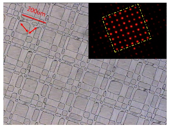
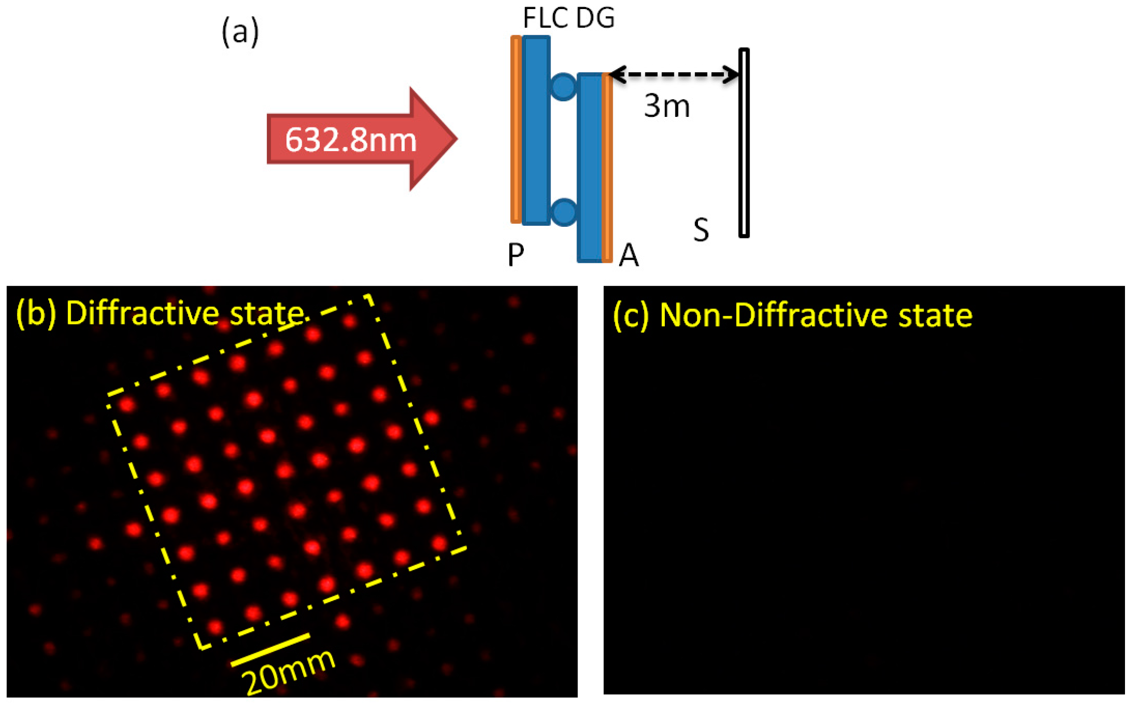
To measure the diffractive performance of the FLC DG, the optical setup shown in
Figure 3a is used, in which a He-Ne laser with wavelength 632.8 nm is used to pass through the prepared FLC DG, and the polarizer (P) and analyzer (A) are set on the two side of the DG with the same configuration as shown in
Figure 2. A signal generator is used to apply electric field on two ITO substrates of the DG. By switching the electric field polarity between +10 V and −10 V, the grating will show switch between diffractive state and non-diffractive state. A screen (S) is used to collect the diffraction patterns for the two states which are shown in
Figure 3b,c. It can be seen that in the diffractive state a 7 × 7 diffractive orders (in dashed yellow square) is generated as shown in
Figure 3b, and a dark non-diffractive state is shown in
Figure 3c. The optical phenomenon consists with the above theoretical analysis.
To provide a detail evaluation of the DG, several quantitative measurements are conducted. The DG is supposed to generate multiple orders with equal intensities, so the intensity distribution for the 7 × 7 orders is important. The DG parameter Uniformity [
36] is applied in our test to study the performance of the DG. The Uniformity is defined as:
, in which
and
represent the maximum and minimum intensity among the 7 × 7 diffractive orders, and the parameter reveals the closer to 0 the better performance of the DG. According to our measurement, the Uniformity equals 0.228 for our FLC DG, which may not be perfect, but implies a reasonable performance of our grating. The diffraction efficiency of the DG is defined as:
], where
is the energy summation of targeted 7 × 7 diffraction orders, and the
is the energy summation of all orders. The measured diffraction efficiency is
. The switching time is measured by adding a photo detector for monitoring the zero order intensity change under switched electric field. By switching the electric field between +10 V and −10 V, the switching time is
for switching from non-diffractive state to diffractive state, and
for switching from diffractive state to non-diffractive state. The switching time is much faster than the commonly used nematic gratings, which normally have switching time in the ms level. Moreover, the contrast between the two states is also measured with the same photo detector. For zero order of the grating, the contrast equals 234 for the intensity in diffractive state over non-diffractive state. The angle spacing between the nearest diffractive orders in horizontal and vertical directions is also measured, which shows
. In principle, the angle spacing can be described with the equation:
, where
is the wavelength of the incident light (
in this test), and
is the pitch of the grating (
in the device). It is easy to verify that the test result of the angle spacing fit well with theory. To increase the angle spacing, the best way is to decrease the pitch of the grating. The pitch equal to 200 μm is used in our experiment, but it is still not the limitation of this technology. Further effort is needed to decrease the pitch, and more importantly, to find out the resolution limit of the patterned aligned FLC device.
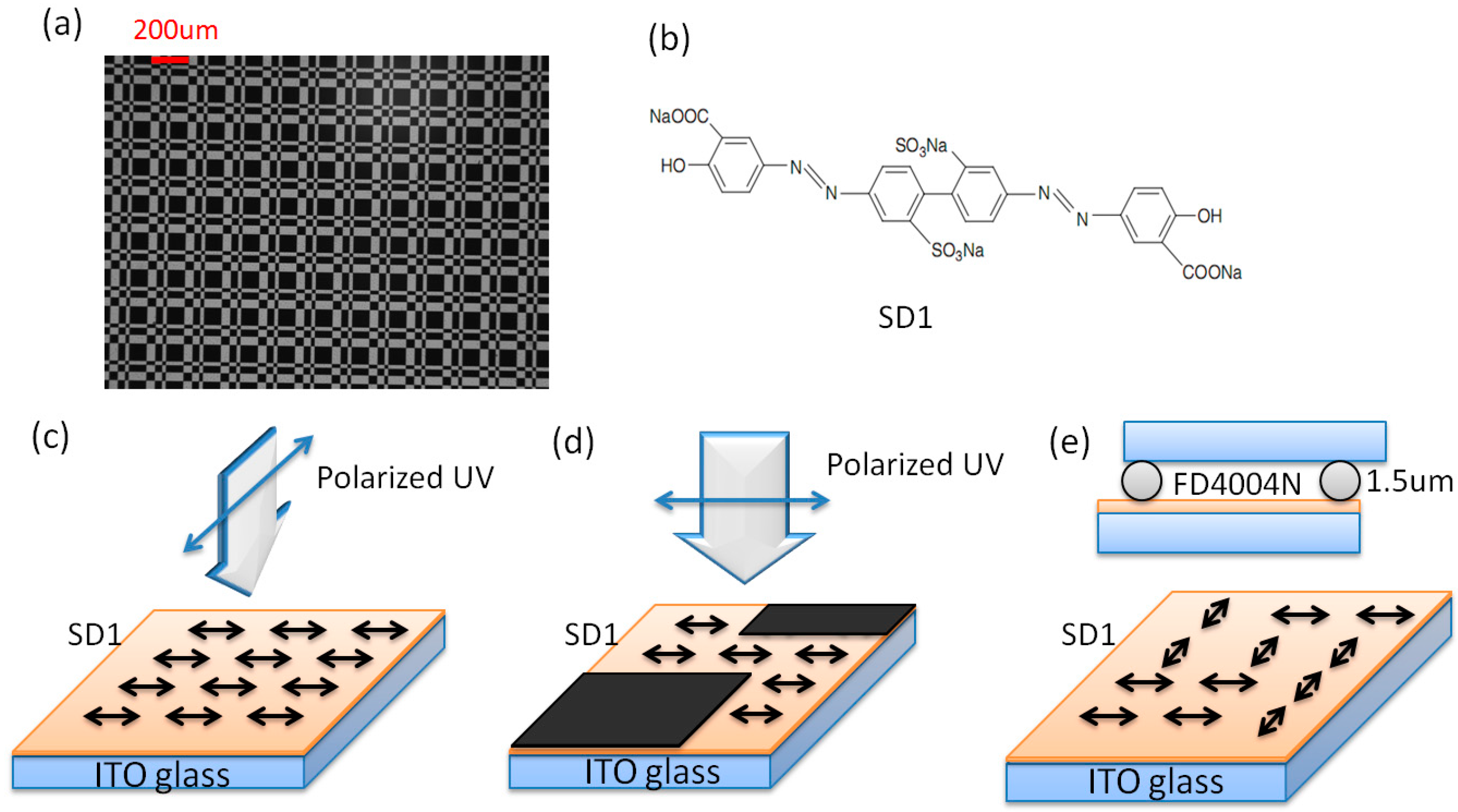
4. Materials and Methods
To fabricate LC DGs, it is necessary to have well designed structures, which are normally defined by the transition points between different phase (0, pi) domains. Since there are lots of well-designed DG phase structures in previous studies, we directly applied the grating structures from reference [
36]. Based on the structures, a chrome mask (photos shown in
Figure 4a) is fabricated, in which the different phase domains are either opaque or transparent. To transfer the domain structure in the mask to the LC device, the photoalignment material azo-dye SD1 (chemical structure shown in
Figure 4b) is used. The SD1 has two important properties [
7]: first, when SD1 layer is exposed with linearly polarized UV or blue light, the LC molecules will be aligned along the direction perpendicular to the exposure light polarization; second, the alignment direction of SD1 is able to be realigned so its alignment direction will follow the latest exposure. By applying these two alignment properties of SD1, a two-step exposure is used to generate a patterned DG alignment structure. The SD1 material is first dissolved in solvent Dimethylformamide (DMF) in 0.5%, and then, the solution is spin-coated on a cleaned ITO glass substrate. After baking for evaporating the DMF solvent, the substrate is then exposed under polarized UV light to generate the first alignment direction, as shown in
Figure 4c. In the second step exposure, the prepared DG chrome mask is placed contacting with the SD1 substrate, which is then exposed again under polarized UV light but in the perpendicular polarized direction comparing with the first exposure, as shown in
Figure 4d. In the second step exposure, only the area that is not blocked by the chrome mask is exposed, within which the alignment direction is changed to be perpendicular relating to the first direction. With these two step exposure, a patterned alignment structure with two orthogonal aligned directions is created. Then a LC cell is assembled with the prepared patterned aligned substrate as one side of the cell and another ITO glass substrate without alignment layer as the other side, as shown in
Figure 4e. The 1.5 μm spacers are deposited between the two substrates to control the cell gap. Then a FLC material FD4004N (Dainippon Ink & Chem Inc., Saitama, Japan) is filled into the prepared LC cell, so the FLC DG is fabricated.


 ,
, 