Review

Graphene-Like ZnO: A Mini Review

1
College of Physics, Optoelectronics and Energy & Collaborative Innovation Center of Suzhou Nano Science and Technology, Soochow University, Suzhou 215006, China
2
Centre of Polymer and Carbon Materials, Polish Academy of Sciences, M. Curie-Sklodowskiej 34, Zabrze 41-819, Poland
3
Leibniz Institute for Solid State and Materials Research Dresden (IFW Dresden), P.O. Box 270116, Dresden D-01171, Germany
4
Department of Energy Science, Department of Physics, Sungkyunkwan University, Suwon 440-746, Korea
5
Center for Nanochemistry, Beijing Science and Engineering Centre for Nanocarbons, Beijing National Laboratory for Molecular Sciences, College of Chemistry and Molecular Engineering, Peking University, Beijing 100871, China
*
Author to whom correspondence should be addressed.
Crystals 2016, 6(8), 100; https://doi.org/10.3390/cryst6080100
Submission received: 2 August 2016 / Revised: 18 August 2016 / Accepted: 18 August 2016 / Published: 22 August 2016

Abstract

:
The isolation of a single layer of graphite, known today as graphene, not only demonstrated amazing new properties but also paved the way for a new class of materials often referred to as two-dimensional (2D) materials. Beyond graphene, other 2D materials include h-BN, transition metal dichalcogenides (TMDs), silicene, and germanene, to name a few. All tend to have exciting physical and chemical properties which appear due to dimensionality effects and modulation of their band structure. A more recent member of the 2D family is graphene-like zinc oxide (g-ZnO) which also holds great promise as a future functional material. This review examines current progress in the synthesis and characterization of g-ZnO. In addition, an overview of works dealing with the properties of g-ZnO both in its pristine form and modified forms (e.g., nano-ribbon, doped material, etc.) is presented. Finally, discussions/studies on the potential applications of g-ZnO are reviewed and discussed.

1. Introduction

Zinc oxide (ZnO), which belongs to the II–VI semiconductor class of materials, has a stable wurtzite structure in standard conditions and it is a key technological material. Its non-centrosymmetric crystallographic wurtzite phase exhibits strong piezoelectric and pyroelectric properties. For these reasons ZnO is frequently used in device fabrication such as in mechanical actuators and piezoelectric sensors, to name a few. Furthermore, ZnO is an n-type semiconductor with a wide band-gap (3.37 eV) and exhibits a high exciton binding energy (60 meV) which makes it an attractive material for short-wavelength optoelectronic applications and room-temperature ultraviolet (UV) luminescence [1]. ZnO is transparent to visible light. Invisible thin film transistors (TFTs) using ZnO as an active channel have achieved much higher field effect mobility values than conventional TFTs [2]. Wurtzite ZnO can also form a diverse family of nano-structures such as nanotubes, nanowires, nanorods, nanobelts, tetrapods, and nanoribbons [1,2].
Over the last decade, after graphene with its extraordinary properties was successfully isolated, the study of two-dimensional (2D) materials became a rapidly growing and important area in nanoscience and nanotechnology. With the decreased thickness of 2D materials, unique electrical, mechanical, chemical and optical properties are introduced. These changes in properties are usually attributed to surface and quantum confinement effects. Recent studies (both theoretical and experimental) [3,4] have shown that when ZnO is thin enough (of the order of a few atoms thick), its wurtzite structure can transform into a 2D stable mono-layer honeycomb structure similar to that of graphene. The graphene-like zinc oxide (g-ZnO) structure is found to be chemically stable according to both theoretical calculations [3,5] and experiments [4]. The electronic and magnetic properties of g-ZnO have been studied [6,7,8,9], as have its elastic and piezoelectric properties [5,10]. The band-gap of g-ZnO is predicted to be 3.57–5.64 eV [6,10] which is larger than that of bulk wurtzite ZnO.

2. Structure of Graphene-Like ZnO (g-ZnO)

According to calculations from Claeyssens et al. [3], ZnO thin films which have a thickness of less than 18 layers will transform from the wurtzite phase to the graphitic-like phase. However, Tusche et al. [4] observed experimentally that the transformation to g-ZnO occurs when a ZnO film is only three or four atomic layers thick. Both calculations and experiments point to g-ZnO being chemically stable. The g-ZnO structure is schematically depicted in Figure 1. The oxygen anions and Zn cations can be seen to form a trigonal-planar coordination instead of the bulk tetrahedral configuration in the wurtzite structure. g-ZnO has a near planar honeycomb structure, which has a hexagonal unit cell (space group P63mc) and lattice parameter a = 3.303 Å (which is 1.6% larger compared to the wurtzite phase) with a bond length between Zn and O of d = 1.92 ± 0.01 Å. However, the values calculated by Chai et al. [11] and Pandey et al. [12] using isolated clusters ranged between 1.817 and 1.930 Å, while Tu and Hu [5] obtained a value of 1.852 Å for a single layer of g-ZnO and Topsakal et al. [6] found a value of 1.895 Å using Density Functional Theory (DFT) approaches. The height difference between the Zn and O atom, μ, within a given layer, was found to be μ = 0.12 ± 0.10 Å [4]. Since sp2 bonding in the trigonal-planar coordination is stronger than the tetrahedral coordinated sp3 bonding in the wurtzite phase, the Zn–O bond length found in the g-ZnO planar honeycomb structure is shorter than that in the bulk wurtzite (or zinc blend) phase. In addition, from experimental observation, the Zn–O bond length between different layers in g-ZnO is larger (up to 2.20 ± 0.10 Å) than that in the wurtzite phase (ca. 11%) [4], which is in agreement with theoretical predictions. Moreover, because the Zn atom radius is larger than that of B, C, N, and O atoms [6], the structure parameters of g-ZnO are significantly larger when compared to graphene and h-BN honeycomb structures.

3. Properties of Graphene-Like ZnO

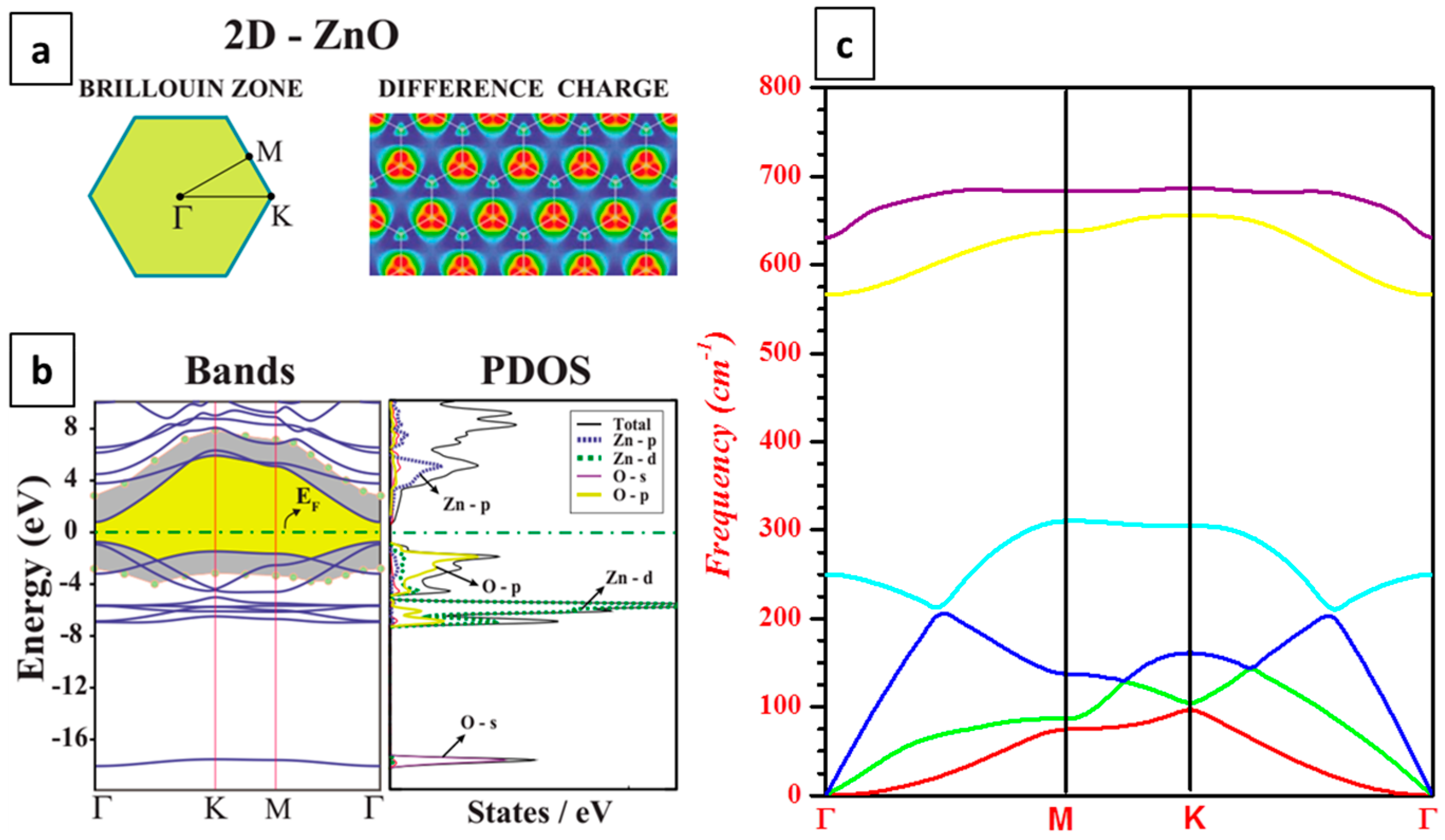
3.1. Electronic Structure

The difference in charge density in the g-ZnO lattice was calculated by Topsakal et al. [6] and their results are presented in Figure 2a. Contour plots of the total charge indicate that a high charge density resides around the O atoms. The different spatial charge density indicates charge transfer from the Zn to the O atoms; in other words, the Zn–O bond has an ionic character. The charge transfer from cation (Zn) to anion (O), δq, in the g-ZnO mono-layer is slightly decreased as compared to the bulk h-ZnO structure (3D hexagonal ZnO). This is attributed to a change between the sp3 hybrid orbital found in bulk h-ZnO and the sp2 hybrid orbital found in the planar g-ZnO structure.
Figure 2b shows the band structure calculated for g-ZnO after optimization [6]. g-ZnO is shown to be a direct band-gap semiconductor with a forbidden energy gap of Egap = 1.68 eV. Tu [10] found an energy gap of Egap = 1.762 eV. However, the actual band-gap is expected to be larger. The underestimation of the band-gap, which is well known in DFT calculations, is attributed to approximations of the electronic correlation effects at the sub-level d, which is caused by the GGA (generalized gradient approximation) function. Using the GW0 method, a direct band-gap at the Γ point of the Brillouin zone is corrected to be 5.64 eV [6]. However, Tu [10] found an energy gap of E gap gw = 3.576 eV using a GW approximation.
In addition, the partial density of states (PDOS, see Figure 2b) showed that the O-2p orbitals primarily contribute to the upper part of the valence band while the Zn–3d orbital contributes to the lower region of the valence band, which is similar to the band contributions found in 3D bulk ZnO crystals. The highest valence band along the Γ–K direction arises from contributions from the O–2pz orbital and a small contribution from the Zn–4pz orbital. The lowest conduction band forms mainly from the Zn–4pz orbital with a small contribution from the O–2pz orbitals. In addition, a small Zn–4pz contribution is confirmed by the PDOS. Thus, the bonding and antibonding combination of O–2pz and Zn–4pz orbitals, forming the π and π* states, constructs the bands at the edges of the conduction and valence bands along the Γ-K direction. Therefore, a planar geometry for g-ZnO mono-layers is expected because of the bonding combination of the pz states.

3.2. Phonon Dispersion Relations

Tu [10] also determined the phonon dispersion relation ω = ω(q) (where ω and q are the phonon frequency and wave number, respectively) from first principle calculations. As shown in Figure 2c, an out-of-plane mode (red curve), an in-plane tangential mode (green curve) and an in-plane radial mode (blue curve) originate from the Γ point of the Brillouin zone and they are all acoustic modes. Near the Γ point, both phonon dispersion curves of the in-plane tangential and radial modes have a linear nature, while the out-of-plane mode has an asymptotic behavior ω(q) = Bq2 with B = 1.385 × 10⁻⁷ m2/s. The sound velocities are vt = 2.801 km/s and vr = 8.095 km/s, which are much smaller than the corresponding velocities (15 km/s and 24 km/s) for graphene [13]. The remaining three branches are optical modes: one out-of-plane mode and two in-plane modes. At the Γ point, their frequencies are 250 cm−1, 566 cm−1, and 631 cm−1, respectively.

3.3. Mechanical Properties

The mechanical response of g-ZnO under strain was investigated by Peng et al. [14] using FT-based first principles calculations. The strain energy per atom is defined as E s = ( E t o t E o ) / n , where Etot is the total energy of the strained system, E0 is the total energy of the strain-free system, and n = 6 is the number of atoms in the unit cell. Es is represented as a function of Lagrangian strains, η, where η ranges from −0.1 to 0.4 (for both compression (η < 0) and tension (η > 0)) in uniaxial armchair, uniaxial zigzag, and biaxial conformations. Es is shown to be anisotropic with strain and nonsymmetrical for compression and tension for all three modes. This nonsymmetry indicates the anharmonicity of the g-ZnO structures. The stresses are derivatives of the strain energies; in the anharmonic region the stresses are not linear with respect to the strain energies. Consequently, the system is susceptible to irreversible structural changes for larger strains. The maximum strain in the anharmonic region is the critical strain. Under armchair deformation the critical strain is 0.18, while for the remaining two directions no critical strain is observed. Peng et al. found that g-ZnO has a nonlinear elastic deformation behavior for the ultimate strain. Values of 0.17, 0.24, and 0.20 were found for the armchair, zigzag, and biaxial directions, respectively. Compared to graphene-like boron nitride (g-BN) and graphene, g-ZnO exhibits a low in-plane stiffness (47.8 N/m) and a large Poisson ratio. The in-plane stiffness of g-ZnO is much lower as compared to h-BN (17% lower), while the ultimate strengths in armchair, zigzag, and biaxial strains, respectively, are 36%, 33%, and 33% lower than for h-BN. The Poisson’s ratio is three times higher than for h-BN. The nonlinear elasticity of g-ZnO was also investigated. By determining the 14 independent components of the second-, third-, fourth- and fifth-order elastic constants from a fitting of stress-strain curves, Peng et al. obtained an accurate continuum description of the elastic properties of g-ZnO.

3.4. Elastic and Piezoelectric Properties

Due to the coupling between elasticity and piezoelectricity, the elastic constants of g-ZnO cannot be directly derived from the phonon dispersion relation. However, Tu [10] reported that by using the ABINIT package the elastic and piezoelectric constants can be calculated directly. From Figure 1c, it can be found that g-ZnO has a three-fold rotation symmetry around the z-axis and a reflection symmetry with respect to the x-axis. Therefore, with zero external electric field, the elasticity (stress-strain relation) can be expressed in the matrix form [15] as:
[ σ 1 σ 2 σ 6 ] = [ c 11 c 12 0 c 12 c 11 0 0 0 c 11 c 12 2 ] [ s 1 s 2 s 6 ]
where c 11 and c 12 are the only two independent elastic constants, σ 1 , σ 2 are the normal stresses and s 1 , s 2 are the normal strains along the x- and y-directions, respectively; σ 6 and s 6 are the in-plane shear stress and shear strain, respectively. Also, the piezoelectric character (with zero external electric field) can be expressed as:
[ P 1 P 2 P 2 0 ] = [ 0 0 d 1 d 1 d 1 0 ] [ s 1 s 2 s 6 ]
where P 2 0 is the spontaneous polarization in the y-direction; P 1 and P 2 are polarizations along the x- and y-directions, respectively; d 1 is the independent piezoelectric constant. The thickness of the g-ZnO mono-layer is implicit in c 11 , c 12 and d 1 , because it is unknown. Based on the relaxed ion model [16], Tu obtained c 11 = 56.8 eV/ZnO, c 12 = 40.3 eV/ZnO, and d 1 = 3.0 pe/ZnO from DFT calculations, where pe = 8.5 × 10⁻³⁰ C m is the atomic unit of the electric dipole moment. The in-plane Young’s modulus (Y = c 11 ( 1 c 12 2 / c 11 2 ) = 28.1 eV/ZnO), shear modulus (G = 1 2 ( c 11 c 12 ) = 8.2 eV/ZnO), and Poisson ratio (ν = c 12 / c 11 = 0.71 ) were derived using the elastic constants.

4. Synthesis of Graphene-Like ZnO

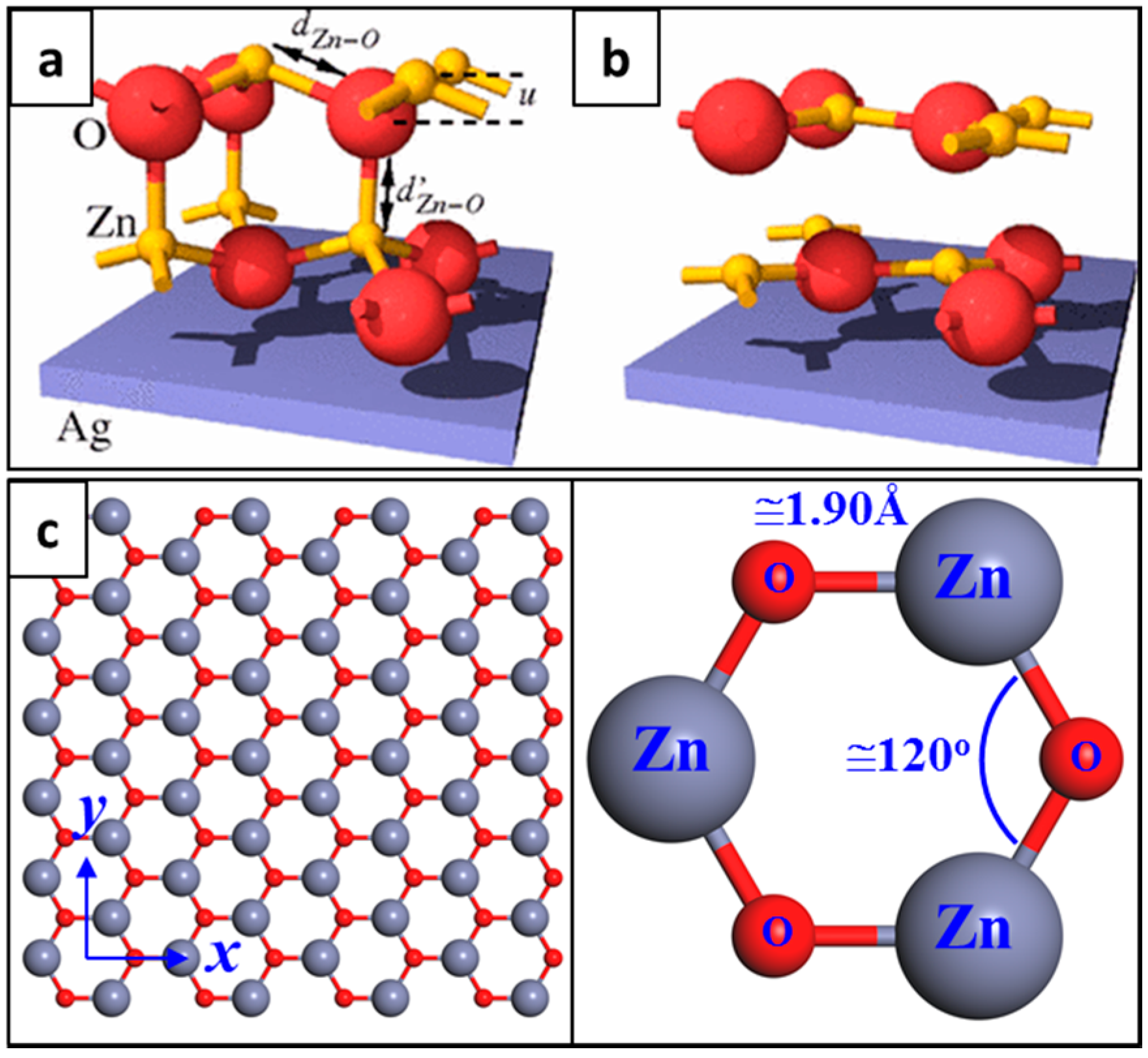
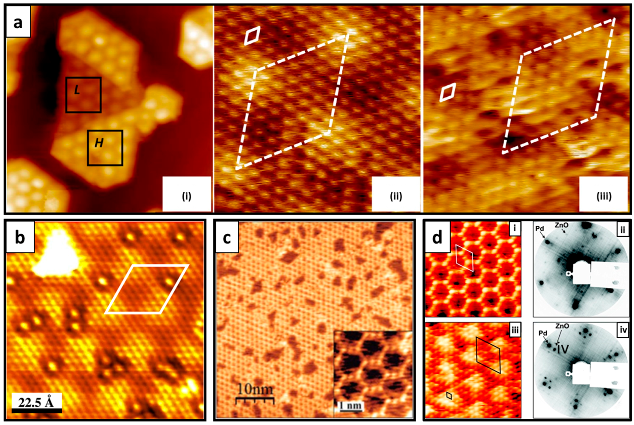
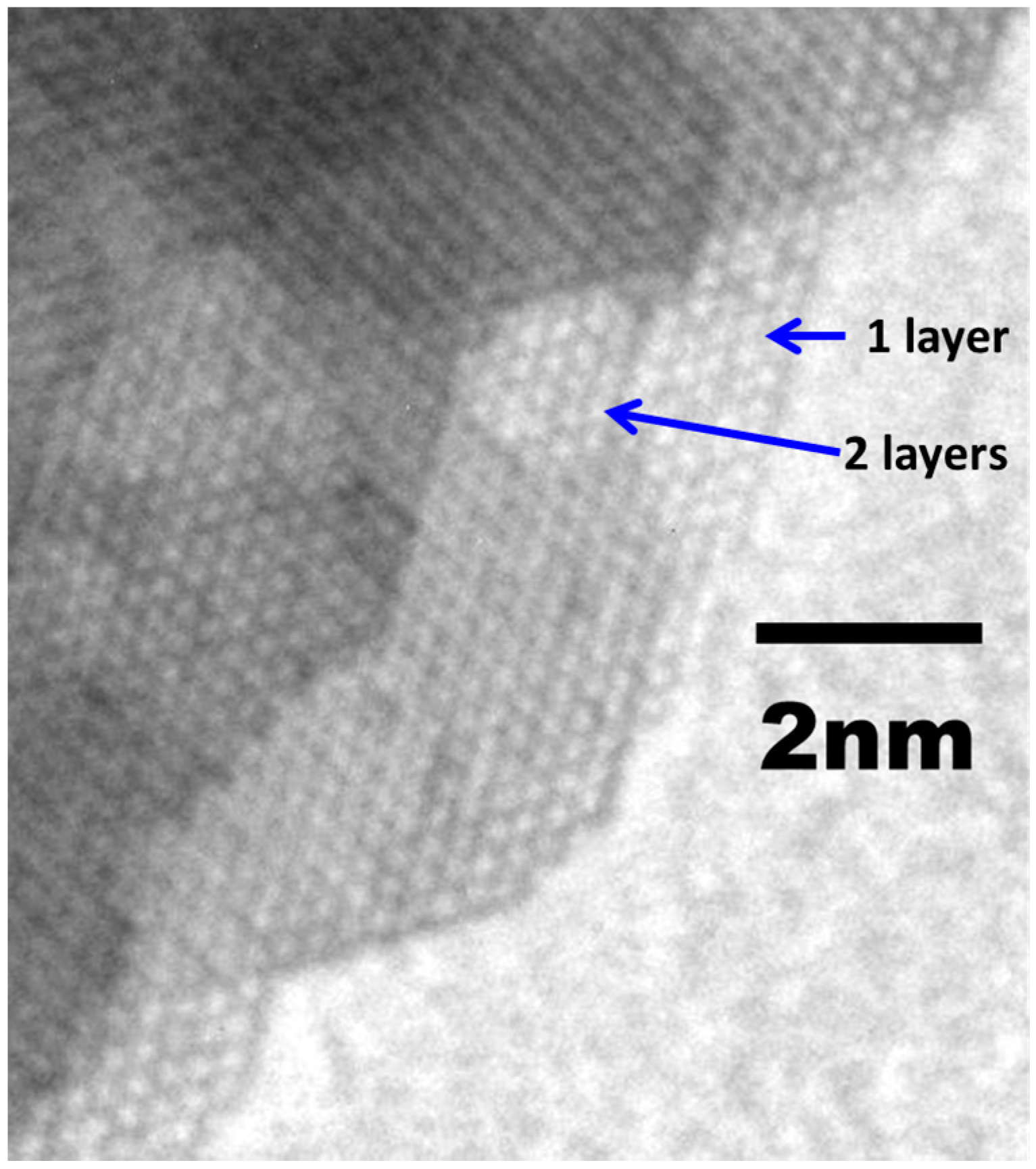
4.1. g-ZnO Growth over a Metal Substrate

The most common method to synthesize g-ZnO layers utilizes a vapor deposition process over a metal substrate under ultrahigh vacuum (UHV) (ranging from ~1 × 10⁻¹⁰ mbar to 5 × 10⁻¹⁰ mbar). In such a process, metallic Zn is deposited on a metal substrate, and oxidized either during a reactive evaporation process or after the Zn deposition (post-oxidation), forming g-ZnO layers. Different metals with their (111) orientations have been exploited as the growth substrates. Examples include Pd(111) [17], Pt(111) [18,19], Au(111) [20], Ag(111) [4,21,22], Cu(111) [22] and Brass(111) [23]. Prior to deposition, the surfaces of the metal substrates were cleaned by mechanical polishing [4] and by cycles of Ar+ ion sputtering followed by annealing in UHV, at 1000 K for Pd [17], 750 K for Ag [4], 670 K [21] or 700 K for Au [20], and 1200 K for Pt [19]. In some cases [17,18,19,22], an annealing step was carried out in the presence of O2 at high temperature (700–800 K) to remove residual carbon. To desorb the residual oxygen, the sample was then flashed to 1000 K in UHV.
g-ZnO layers can be obtained by first depositing pure Zn at room temperature on to a clean metal substrate by heating a Zn rod using a Knudsen cell [17,21]; in other cases, pulsed laser deposition [4], an electron beam–assisted evaporator [20] or applied current through a thoriated tungsten wire wrapped around the Zn rod can be used [18,19,22]. When oxygen is injected, it is done so at relatively high pressures ranging from ~10−8 and ~10−5 mbar either during or after Zn deposition at room temperature, followed by an annealing step in UHV (the annealing temperature depends on the metal substrate and typically varies between 550 K and 680 K). Usually the post-oxidation (injecting O2 after Zn deposition) technique is used for sub-mono-layer oxide coverage, whereas the reactive evaporation (injecting O2 during Zn deposition) method is preferred for coverage >1 mono-layer in order to avoid possible alloying at the substrate interface.
Often the UHV chamber is equipped with a scanning tunneling microscope (STM) to enable the crystal structure to be determined at the atomic scale and also to obtain the thickness of the g-ZnO after synthesis (Figure 3). Figure 3a shows typical room-temperature STM images of g-ZnO grown over Au(111) [20]. Panel (i) clearly shows the hexagonal Moiré pattern of ZnO over Au(111) as seen on both low-ZnO (where the height of the flake is measured in STM to be ~3.5 Å) and high-ZnO (where the height of the flake is ~5.5 Å from the Au plane) crystals. On both the low– and high–g-ZnO structures, a clear atomic structure consisting of a hexagonal unit cell with a lattice parameter of ∼3.3 Å is determined by STM (see panels ii and iii of Figure 3a). In addition, it should be noticed that the atomic unit cell and the Moiré repeating unit have the same registry (highlighted by solid and dashed cells), indicating that the ZnO lattice is in alignment with the Au(111) lattice. The coinciding lattice of the g-ZnO with the metal substrate is also observed on the Ag(111) [4] surface which is reflected in a Moiré pattern (see the atomic resolution STM micrograph shown in Figure 3b). In addition to the Moiré pattern, the short period contrast between individual ZnO unit cells is observed, and the surface is atomically flat with only some isolated defects. Other examples of g-ZnO flakes are also provided in Figure 3c, where Zn was deposited in vacuum onto an oxygen pre-covered Pt(111) surface [18]. A Moiré pattern from g-ZnO and Pt(111) is clearly observed in the STM image. A high resolution STM image (inset figure) reveals the honeycomb-like (4 × 4) configuration (in which four Pt(111) surface unit cells coincide with four g-ZnO cells). Weirum et al. [17] reported that the structure and stoichiometry of g-ZnO over-layers depend strongly on the oxygen pressure and zinc coverage. At sub-mono-layer coverages two planar oxide phases with (4 × 4) and (6 × 6) unit cells can coexist on a Pd(111) surface. An example is provided in Figure 3d.

4.2. Hydrothermal Growth

A solution-based approach for the synthesis of g-ZnO has recently been reported by Sahoo et al. [24]. In that work, g-ZnO structures were synthesized using a mild hydrothermal technique. An aqueous solution (30 mL) with zinc nitrate hexahydrate (Zn(NO3)2.6H2O), 0.005 M hexamethylene tetramine (HMT) and 0.001 M sodium citrate (Na3C6H5O7) was prepared. The aqueous solution was then placed in a Teflon container and sealed in a steel autoclave. The autoclave was then placed in an oven at 95 °C for 3 h. After completion of the reaction, the sample was collected by filtration and then dried at 60 °C for 12 h. The crystal structure of the as-produced material was subsequently characterized using transmission electron microscopy (TEM). Figure 4 shows a micrograph of a typical ZnO crystallite nanoparticle with high resolution HR-TEM, suggesting the presence of single-layer and bi-layer g-ZnO crystals at the edge of the crystal. However, the TEM characterization in this study was insufficient to unambiguously determine the presence of g-ZnO.

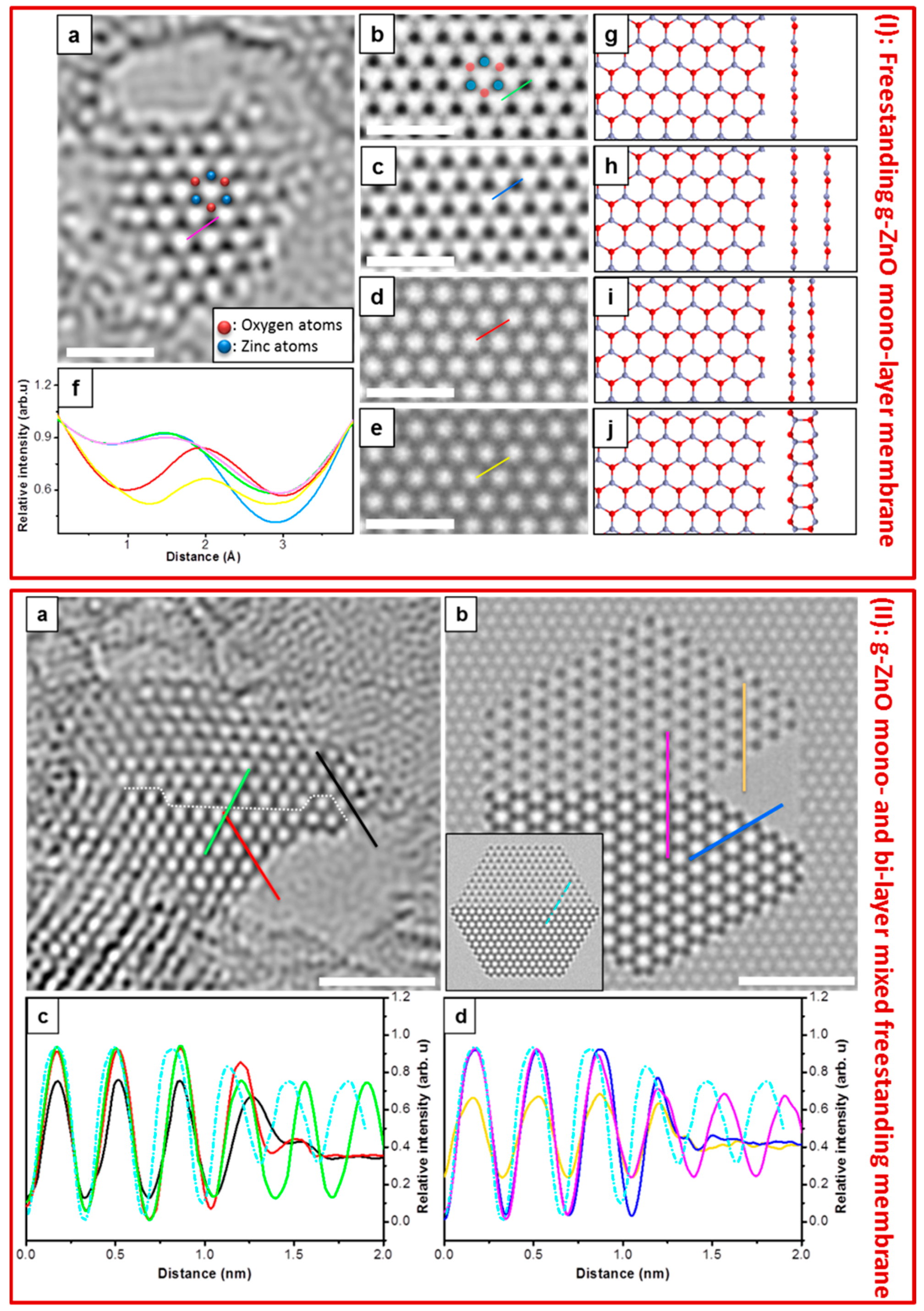
4.3. Free-Standing Formation of g-ZnO in Graphene Pores

The vast majority of g-ZnO synthesis routes require some kind of substrate. This has the drawback that there may be interactions between the g-ZnO layer or layers with the substrate, in turn leading to modified or altered physico-chemical properties. Recently, Quang et al. [25] reported an in situ approach for the fabrication of freestanding mono- and bi-layer g-ZnO membranes residing in graphene pores. The fabrication technique is based on the thermal decomposition of zinc acetylacetonate (Zn(C5H7O2)2) (zinc-acac) over graphene followed by an electron beam–driven reaction. Initially, a TEM grid with Chemical Vapor Deposition (CVD)-grown mono-layer graphene transferred on top was placed and sealed under vacuum in a glass vial, along with a small amount of zinc-acac powder. The sealed vial was then annealed at 300 °C for 12 h to decompose the zinc-acac. Thereafter, the vial was opened and the TEM grid plus treated graphene was placed in a TEM column. Upon electron beam irradiation, freestanding g-ZnO membranes can be synthesized within graphene pores.
An example of freestanding mono- and bi-layer g-ZnO in a graphene pore is provided in Figure 5. Frame (I) shows a typical example of a freestanding mono-layer g-ZnO along with various image simulations for mono- and bi-layer g-ZnO and also for a wurtzite ZnO structure. Through comparative studies, those simulations confirm the presence of freestanding g-ZnO, whereas relative intensity measurements can be used to determine the number of layers. Panel a shows a TEM image of a freestanding mono-layer of g-ZnO in a graphene pore. Image simulations for mono-layer g-ZnO (panel b) and the bi-layer T1 and T2 stacking configurations are provided in panels c and d, respectively, and bi-layer wurtzite is presented in panel e for a visual comparison. Frame (II) shows a TEM image of a membrane with a mix of layers (panel a) and image simulations for both g-ZnO and wurtzite ZnO (panel b). Various intensity profiles are shown in panels c and d. This study was the first to confirm the existence of freestanding mono- and bi-layer g-ZnO.

5. Modification and Potential Applications of g-ZnO

5.1. g-ZnO Structure Modification

When a small fraction of foreign atoms is introduced into a pure, intrinsic semiconductor material, it can produce dramatic changes in its electrical properties. This process is called doping. It is well known that the properties of 2D materials such as graphene, transition metal dichalcogenides, silicene and hexagonal boron nitride can be easily modified through doping. Since the discovery of g-ZnO, various studies looking at its structure modification to alter its electrical properties have been undertaken.

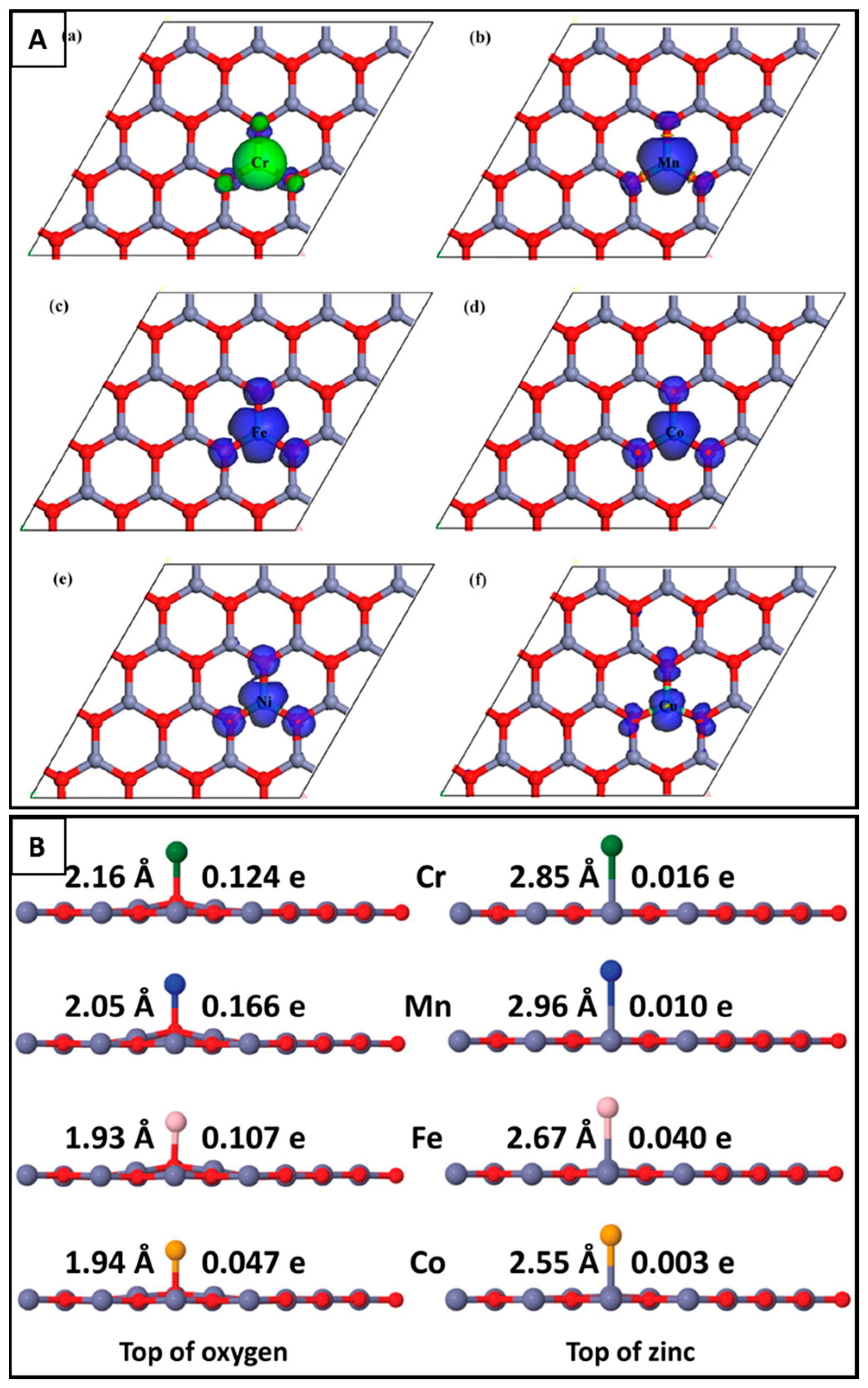
5.1.1. Doping and Decorating of g-ZnO

Several studies have demonstrated that the electronic and magnetic characteristics of g-ZnO can be tuned by doping with foreign atoms. Tuning g-ZnO by doping could be a means to exploit the material for electronic and spintronic applications. Schmidt et al. [26] reported that Co-doped g-ZnO exhibits ferromagnetic coupling. This ferromagnetic coupling is a direct consequence of the two-dimensional character (i.e., 2D confinement) of the g-ZnO structure. Through first principle calculations they showed that Co atoms can substitute Zn atoms in g-ZnO in a barrier-free process. The presence of Co atoms introduces a Jahn–Teller distortion in the system, reducing the symmetry of the sheet, leading to a strong direct exchange interaction between the 3d orbital of the Co atoms. He et al. [27] studied the adsorption of Mn atoms on g-ZnO and single-wall ZnO nanotubes using first principle calculations. Their data showed that for Mn-doped g-ZnO, the H site (where an Mn atom is located over the center of a hexagon) is the most energetically favorable site for adsorption with a relatively large binding energy of 1.24 eV. When the Mn atom is adsorbed at an H site, it can form bonds with its three nearest-neighbor oxygen atoms. This process tends to push its three nearest-neighbor Zn atoms out of plane. Thus, the total magnetic moment per Mn atom of the Mn-doped g-ZnO sheet is 5.0 μB (almost the same as that of a free Mn atom) with spin polarization (for both majority and minority spin) as compared to the non-magnetic properties of pristine g-ZnO.
From a comprehensive first principle study on transition metal (TM)-doped g-ZnO, Ren et al. [28] found that 3d TM (Sc, Ti, V, Cr, Mn, Fe, Co, Ni and Cu) can efficiently dope the g-ZnO material by substitution of Zn atoms (formation energy ranged from −6.319 to −0.132 eV). This TM doping can modify the electronic and magnetic properties of g-ZnO. However, not all 3d TMs can change the magnetic behavior of the system. Ren’s calculations show no magnetism (0 μB) in Sc-, Ti- and V-doped g-ZnO mono-layers, while the local magnetic moments of Cr, Mn, Fe, Co, Ni, and Cu are −3.319, 4.681, 3.575, 2.676, 1.545, and 0.578 μB, respectively. The local magnetic moments data show that the Cr ion induces antiferromagnetic interactions in the nearest-neighbor O ion, while Mn, Fe, Co, Ni, and Cu ions induce ferromagnetic interactions in the nearest-neighbor O ion. By looking at the spin charge density distribution (Figure 6A), it was found that the magnetism originates and arises mainly due to the TM atoms, while the nearest-neighbor O atoms of TM atoms have only a small contribution to the total magnetic moments. Panel a shows that the main minority spin (spin-down) density is localized around the Cr atom where the total moment per supercell is −3.255 μB and the local moment for the Cr dopant is −3.211 μB, while Mn-doped g-ZnO has a total magnetic moment per supercell of 4.860 μB and the local moment of Mn is 4.681 μB. The magnetism of Mn-doped g-ZnO mostly occurs by the Mn atom, while the nearest-neighbor O atoms of an Mn atom provide only a small contribution to the total magnetic moment as shown in panel b. Similarly, the majority spin (spin-up) density is localized around Fe, Co, Ni or Cu atoms (see panel c–f, respectively), which indicates that the major contribution to the total magnetic moments of TM-doped g-ZnO is from dopant atoms. The magnetic moment is attributed to the strong p–d mixing of O and TM orbitals. Furthermore, the electronic structure of the g-ZnO mono-layer is significantly changed after doping. The results show that Sc, Ti, and V do not modify the magnetic properties of g-ZnO; however, the energy band-gap can be tuned by these foreign atoms. Sc-doped g-ZnO yields a direct band-gap of 2.084 eV; in Ti-doped g-ZnO, there is a small gap of 0.134 eV, making it close to a semi-metal, while V-doped g-ZnO remains semiconducting with an indirect band-gap of 0.561 eV. In summary, Cr-doped g-ZnO mono-layers have a metallic behavior whereas Mn-, Fe-, Co-, Ni-, Cu-doped g-ZnO have a semiconducting behavior with band-gaps of 0.689, 1.057, 1.518, 1.648, 1.798 eV, respectively, for the majority spin state and 2.164, 0.516, 1.142, 0.181, 0.780 eV, respectively, for the minority spin state.
In the doping process, the TM atoms are initially adsorbed on the surface of g-ZnO, and then the substitution of Zn by a TM atom may occur when its kinetic energy exceeds the energy barrier of the adsorption-substitution transformation. Lei et al. [29] demonstrated that the substitution configuration is more stable than the adsorption one (determined via binding energy characterization). However, only vanadium was found to substitute without any energy barrier. The replacement of Zn by Cr, Mn, Fe, or Co requires overcoming an energy barrier (tens to hundreds meV) during the adsorption-substitution transformation. Thus, Cr-Co prefers adsorption configurations when deposited on g-ZnO. From Cr to Co, the binding energy of TO-site (TM on top of oxygen) adsorption is the highest as compared to the TZn site (TM on top of a zinc atom) and H site (TM over the center of a hexagon). Figure 6B shows molecular dynamic simulations for the optimized structure of TO-site adsorption for Cr–Co. The short TM–O bonds in a TO adsorption configuration (left panel) can be explained by the large electronegativity difference between TM and O which leads to the occurrence of charge transfer from the TM atom to the O atom. On the contrary, for the TZn-site adsorption configuration, the longer TM–Zn bond is attributed to negligible charge transfer from the TM atom to Zn, which leads to lower binding energy than for TO-site adsorption configurations (right panel). Interestingly, the molecular dynamic calculations show that when a Cr or Mn atom is deposited on g-ZnO, the hollow-site configuration is preferred to the TO site. This is due to the more stable constraint given by the three-coordination structure of an H site as compared with the O site. Therefore, Cr, Mn prefer H-site adsorption configurations while the TO-site configuration is more favorable for Fe and Co. In addition, except for Cr, the magnetic moment of TM-decorated g-ZnO is the same as that of a free TM atom and the work function of g-ZnO can be significantly decreased by TM decoration from 4.94 eV to 3.17–3.82 eV. In this manner the magnetic and electronic properties of G-ZnO are tunable by TM decoration.
In addition to transition metal doping, the feasibility of tuning the magnetic and electronic properties through doping with non-metal elements in g-ZnO mono-layers has been explored for O atom substitution with B, C or N atoms as reported by Guo et al. [7]. Their calculations show that doped g-ZnO mono-layers with one B or C atom per supercell form a ferromagnetic half metal, while those with one N atom per supercell form a ferromagnetic semiconductor, in which the total magnetic moment is mainly contributed by the dopant. In the case of two O atoms (per supercell) substituted by C or B, the magnetic properties vary, depending on the distance between the two dopant atoms. Once two carbon or boron atoms in the g-ZnO mono-layer supercell are close enough to form dimer pairs, they can modify the g-ZnO into an n-type semiconductor with a nonmagnetic ground state. The doped g-ZnO can undergo nonmagnetic–antiferromagnetic–ferromagnetic and semiconductor–half metal transitions, as the distance between two C or B atoms increases. On the other hand, two N atoms doping a g-ZnO mono-layer (per supercell) form a p-type semiconductor with an antiferromagnetic ground state. The calculations show that the magnetic properties are independent of the distance between the two N atoms.

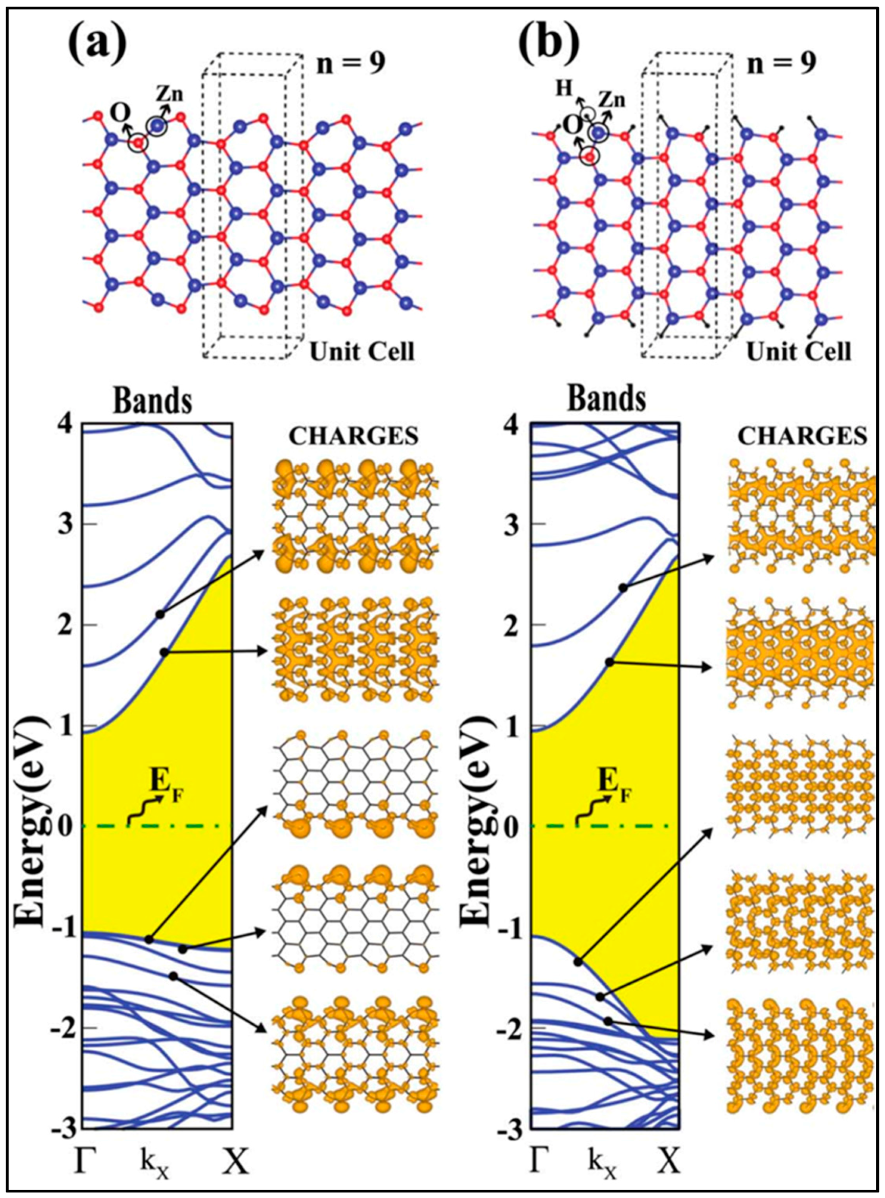
5.1.2. g-ZnO Nanoribbon

Topsakal et al. [6] provided a comprehensive study of the electronic structure of hydrogen-passivated as well as bare armchair (a-ZnO) and zigzag (z-ZnO) g-ZnO nanoribbons using ab initio molecular dynamic calculations. Bare and hydrogen-passivated a-ZnO(n) (where the nanoribbon width is given in terms of the n number of Zn–O pairs in their unit cells, with n = 9) nanoribbons are found to be nonmagnetic semiconductors with direct band-gaps as shown in Figure 7. The atoms at the edges of the bare a-ZnO are reconstructed (Figure 7a, top). GGA calculations show that the energy band-gap of a bare a-ZnO is direct with a gap value of 1.92 eV which is larger than the band-gap of single-layer g-ZnO. Band-decomposed charge-density analysis of a-ZnO(9) (Figure 7a, bottom) shows the charge distribution of the band structure: (i) In the valence band, the highest bands are degenerated and their charge accumulates on the oxygen edge atoms, and the third band from the top is also distributed mainly at the edge of the ribbon. (ii) In the conduction band, while the charge of the lowest band is distributed uniformly in the ribbon, the charge of the second band is mostly distributed at the dangling bonds on the edges of the ribbon. The electronic band structure is altered by hydrogen termination at the edges of the nanoribbon. As seen in Figure 7b, hydrogen passivation reduces the reconstruction of edge atoms. Eventually, band-decomposed charge-density studies show that the edge state bands are discarded from the band-gap and switched by dispersive bands with a uniform charge distribution in the ribbon with a band-gap of ∼1.98 eV. The bare and H-passivated a-ZnO band-gaps vary as a function of their widths (number of Zn–O pairs n). Narrow nanoribbons have relatively larger band-gaps due to quantum-confinement effects.
In contrast to a-ZnO nanoribbons, z-ZnO show a metallic character regardless of their width, and bare z-ZnO nanoribbons are ferromagnetic due to their edge states which is in agreement with other studies on g-ZnO nanoribbons [30,31]. In bare z-ZnO, the total magnetic moment of the system was calculated as 0.57 μB per unit cell. The atoms near the oxygen-terminated edge of the ribbons acquire magnetic moments. The splitting of the spin-up and spin-down bands around the Fermi level is also observed in bare z-ZnO. However, this splitting is removed once O- and Zn-terminated edges are passivated with hydrogen atoms. In addition, the zigzag nanoribbon becomes a nonmagnetic metal.
Topsakal et al. [6] also investigated the mechanical properties of g-ZnO nanoribbons. Under uniaxial strain ϵ , g-ZnO nanoribbons show elastic deformation in both harmonic and inharmonic ranges. The elastic deformation range of both a-ZnO and z-ZnO ends at a certain uniaxial strain point (called the yielding point of the ribbon) with a sharp fall of the total energy, and the nanoribbon deforms plastically. In the elastic range, hexagons are uniformly deformed and the honeycomb-like atomic structure is maintained. After the yielding point is reached, some of the hexagons are modified and reconstruct to different polygons (being smaller or larger than hexagons) and a net magnetic moment may develop in the polygons. Calculations of the force constants and in-plane stiffness indicate that the stiffness of ZnO nanoribbons is significantly smaller than those of graphene and BN nanoribbons. This is due to the g-ZnO honeycomb structure having a larger unit cell than that of graphene and BN honeycomb structures.

5.2. Potential Applications

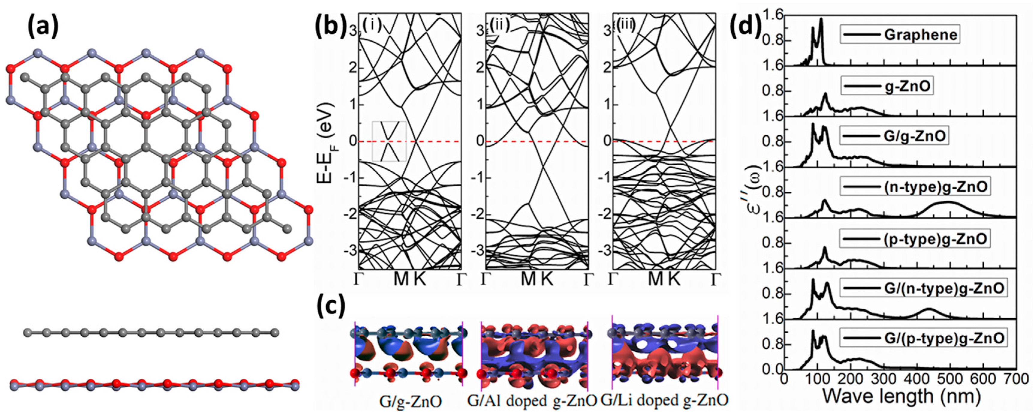
5.2.1. Graphene–g-ZnO Heterostructures

Recently, Hu et al. [32] explored the possibility of a g-ZnO layer as a substrate for graphene using first principle calculations (Figure 8). The electronic structures and optical properties of a graphene/g-ZnO (G/g-ZnO) heterojunction were investigated. The interaction between graphene and g-ZnO was found to be through weak van der Waals (vdW) interactions with a typical equilibrium spacing of 3.14 Å. The electronic band structure of G/g-ZnO (Figure 8b, left panel) shows that only a small band-gap (5 meV) is opened. Even when g-ZnO is doped with Al and Li, thus forming G/Al-doped g-ZnO and G/Li-doped g-ZnO heterojunctions, there is only a tiny band-gap opening (7 and 11 meV, respectively, see Figure 8b, middle and right panels). The Fermi level of a G/g-ZnO (pristine) structure remains in the induced gap, indicating no charge transfer occurs between graphene and a g-ZnO mono-layer. Thus, the intrinsic electronic properties of graphene, particularly high carrier mobility, can be maintained in a G/g-ZnO structure. The inhomogeneous charge density in the g-ZnO substrate induces a charge redistribution in the graphene plane (Figure 8c, left panel), forming intra-layer electron-hole puddles, which may significantly enhance the electron conductivity and/or generate new photovoltaic and catalytic activities. Furthermore, the Fermi velocity at the Dirac point of graphene in the G/g-ZnO structure is nearly similar compared to freestanding graphene. Therefore, pristine g-ZnO would be an ideal substrate for graphene in which its electronic structure is preserved. A different charge rearrangement was found in G/Al-doped g-ZnO and G/Li-doped g-ZnO structures (Figure 8c, middle and right panels). Electron-hole pairs are found to be well separated at the interfaces of G/doped g-ZnO structures. The optical properties of the G/g-ZnO and G/doped g-ZnO structures were also studied (Figure 8d). Compared to g-ZnO mono-layers, the G/g-ZnO structure displays a more effective UV absorption and enhanced visible light response. G/doped g-ZnO structures also exhibit a higher effective UV absorption as compared to doped g-ZnO mono-layers. The improved optical properties in the G/g-ZnO structure (pristine and doped) are promising for photocatalytic and photovoltaic applications.
In another case study, Yao et al. [33] also investigated the electronic structure and optical properties of G/g-ZnO with and without oxygen vacancies using first principles calculations. The results were similar to those found by Hu et al. The data showed that graphene weakly interacts with g-ZnO as well as g-ZnO with oxygen vacancies. Moreover, in both cases G/g-ZnO with and without oxygen vacancies is able to maintain graphene’s intrinsic electronic properties, high carrier mobility, and optical absorptions.

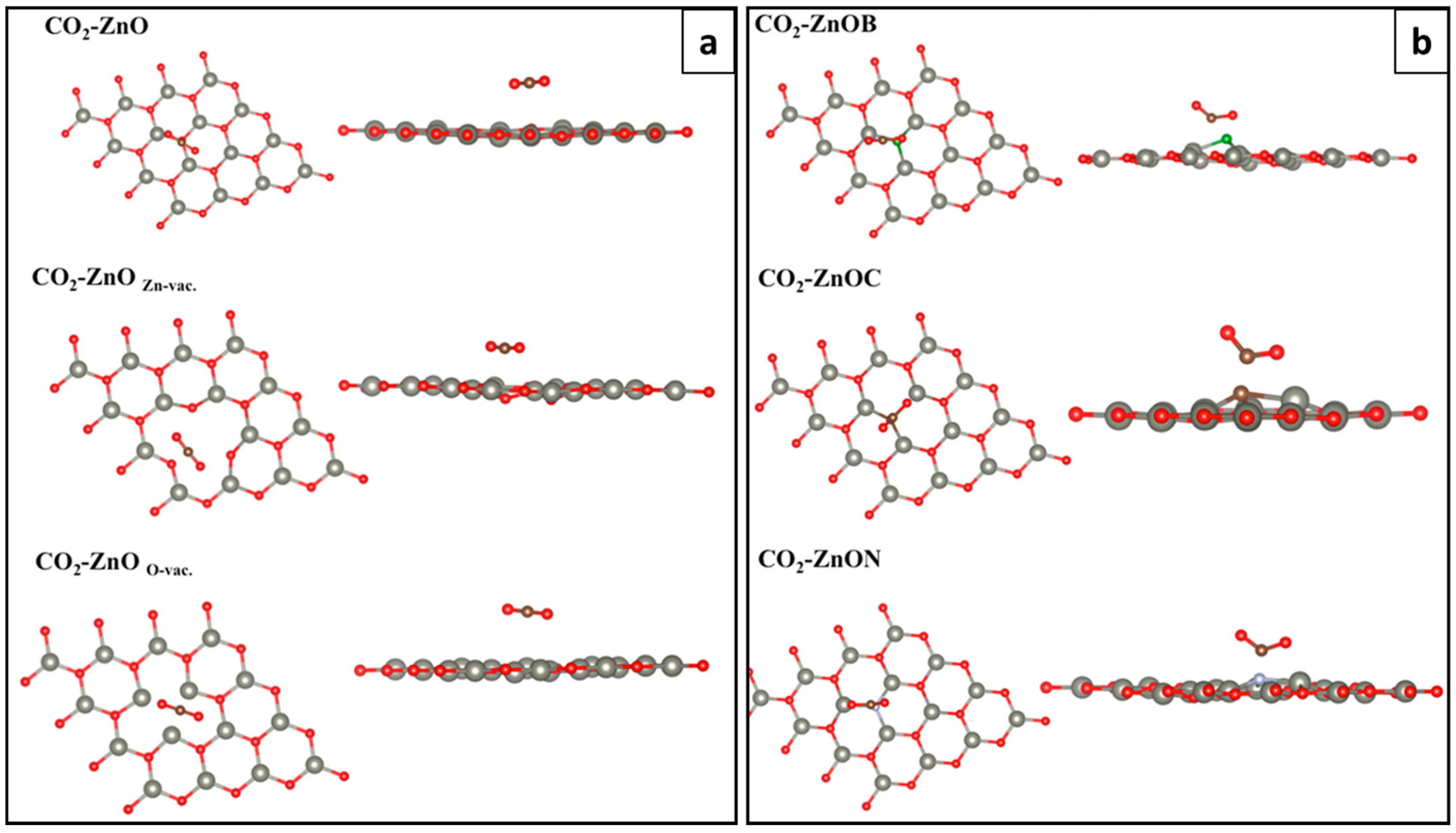
5.2.2. CO and CO2 Physisorption of g-ZnO

Zhang et al. [34] have reported that doped g-ZnO exhibits strong chemisorption of the CO molecule by forming A-CO (where A=B, N or C dopants) in contrast to weak physisorption on pristine g-ZnO. The adsorbed CO slightly pulls the A atom out of the sheet plane, viz. the A site is transformed from an sp2 hybridization to a more sp3-like hybridization. Total charge density calculations show that large charge transfer occurs between the doped g-ZnO and a CO molecule, while little charge is transferred between pristine g-ZnO and a CO molecule. Moreover, the shorter bond lengths of A–CO (1.43 Å, 1.24 Å, 1.32 Å for B, N and C, respectively, as compared to pristine g-ZnO, 2.32 Å) and a higher binding energy (−4.05, −2.77, −5.65 eV for B, N and C, respectively, as compared to pristine g-ZnO −0.35 eV) clearly indicate that a chemical bond can form during the adsorption process.
In the same vein, Rao et al. [35] investigated the interaction of CO2 with pristine, defective and non-metal-doped g-ZnO mono-layers (Figure 9) in terms of their efficiency to capture CO2 and hence their potential for cleaning our atmosphere and purifying fuel engine emissions. The calculations show that a CO2 molecule favors adsorption on the top of an O location and favors a horizontal alignment with respect to the pristine g-ZnO mono-layer (ML) (Figure 9a, top). The adsorption energy of the CO2 molecule on a g-ZnO mono-layer is found to be −0.20 eV, indicating physisorption with a CO2–gZnO distance of 2.92 Å. The CO2 adsorption on defective as well as non-metal (B, C, N), substitutionally doped g-ZnO mono-layers was also investigated. The adsorption of CO2 at oxygen and zinc vacancies was explored in the study on defective g-ZnO (Figure 9a, center and bottom). In the case of a Zn vacancy, the adsorption of CO2 was enhanced by up to 80%. Figure 9b (top-bottom) shows the most favorable adsorption configuration of CO2 on doped g-ZnOB, g-ZnOC, and g-ZnON (where the O atom is substituted by B, C or N, respectively). It was found that a CO2 molecule prefers to reside on top of the foreign atom and that the substitutional atom is pulled towards the CO2 molecule. The adsorption energy of CO2 dramatically increases to −1.77 eV, −1.33 eV and −0.80 eV with adsorption distances of 1.53 Å, 1.44 Å and 1.41 Å for B, C and N atoms, respectively. This indicates a chemisorption mechanism with a large binding energy and a short adsorption distance and stands in contrast with physisorption on pristine g-ZnO.

5.2.3. Catalytic Activity g-ZnO

Ma et al. [36] found that Al-doped g-ZnO mono-layers (in which Al atoms substitute host Zn atoms) show good catalytic activity for CO oxidation via the Eley–Rideal mechanism with a two-step route. In this mechanism, the first CO molecule directly interacts with the pre-adsorbed O2 molecule, forming a carbonate-like CO3 complex as an intermediate state. This process is exothermic by 3.93 eV and the reaction requires only a small barrier of 0.006 eV to be overcome. The second CO molecule initially adsorbed on top of one Zn atom near the doped Al atom then approaches the CO3 complex to form two CO2 molecules with an energy barrier of 0.79 eV. Two CO2 molecules are produced with an adsorption energy of 0.46 eV with respect to two free CO2 molecules in the gas phase. Since the energy released in this step (0.79 eV) can easily surmount the adsorption energy, these two CO2 molecules can be released rather easily from the g-ZnO sheet. The reaction proceeds rapidly at low temperature, suggesting that Al-doped g-ZnO mono-layers could be an efficient catalyst for CO oxidation at low temperature.

6. Summary and Outlook

Following initial theoretical predictions, g-ZnO has now been proven experimentally both as a supported material and in its freestanding form. Early works, mostly theoretical, suggest interesting properties for this new 2D material, not only in its pristine form, but, for example, as a nanoribbon in which the properties (e.g., band-gap) depend on the nanoribbon’s width and edge termination, similar to graphene nanoribbons. Doping the material can also allow one to tailor certain properties, particularly magnetic properties. In addition, several studies point to useful CO and CO2 physisorption on g-ZnO, and the influence of doping. Moreover, defective g-ZnO is shown to be an excellent material for CO2 capture. In terms of the future for graphene-like ZnO, while it is rather difficult to make predictions, one can anticipate new synthesis approaches arising. Unlike other 2D layer materials, due to the small number of layers that form, exfoliation is an unlikely route. However, as with so many nanomaterials, CVD is a technique that will probably develop as the main route for synthetic g-ZnO. Other routes, such as wet chemical approaches may also emerge. Moreover, as more g-ZnO is produced, more studies will elucidate its properties, and it will be these (its properties) that will determine just how big the success of g-ZnO will be. That said, even though the investigation and use of g-ZnO is still in its early phase, what we have already learned about the material is extremely interesting and this bodes well for g-ZnO use in real applications in the future.

Acknowledgments

Huy Q. Ta and Mark H. Rümmeli thank Soochow University for its support. Alicja Bachmatiuk thanks the National Science Center for the financial support within the frames of the Sonata Program (Grant agreement 2014/13/D/ST5/02853). Mark H. Rümmeli acknowledges the National Science Center Opus Program (Grant agreement 2015/19/B/ST5/03399) and the National Science Foundation China (NSFC. Project 51672181).

Author Contributions

All authors contributed to the writing and production of this manuscript.

Conflicts of Interest

The authors declare no competing financial interests.

References

  1. Wang, Z.L. Zinc oxide nanostructures: Growth, properties and applications. J. Phys. Condens. Matter 2004, 16, 829–858. [Google Scholar] [CrossRef]
  2. Fan, Z.; Lu, J.G. Zinc oxide nanostructures: Synthesis and properties. J Nanosci. Nanotechnol. 2005, 5, 1561–1573. [Google Scholar] [CrossRef] [PubMed]
  3. Claeyssens, F.; Freeman, C.L.; Allan, N.L.; Sun, Y.; Ashfolda, M.N.R.; Harding, J.H. Growth of ZnO thin films-experiment and theory. J. Mater. Chem. 2005, 15, 139–148. [Google Scholar] [CrossRef]
  4. Tusche, C.; Meyerheim, H.L.; Kirschner, J. Observation of depolarized ZnO(0001) mono-layers: Formation of unreconstructed planar sheets. Phys. Rev. Lett. 2007, 99, 026102. [Google Scholar] [CrossRef] [PubMed]
  5. Tu, Z.C.; Hu, X. Elasticity and piezoelectricity of zinc oxide crystals, single layers, and possible single-walled nanotubes. Phys. Rev. B 2006, 74, 035434. [Google Scholar] [CrossRef]
  6. Topsakal, M.; Cahangirov, S.; Bekaroglu, E.; Ciraci, S. First-principles study of zinc oxide honeycomb structures. Phys. Rev. B 2009, 80, 235119. [Google Scholar] [CrossRef]
  7. Guo, H.; Zhao, Y.; Lu, N.; Kan, E.; Zeng, X.C.; Wu, X.; Yang, J. Tunable magnetism in a nonmetal-substituted ZnO mono-layer: A first-principles study. J. Phys. Chem. C 2012, 116, 11336–11342. [Google Scholar] [CrossRef]
  8. Zheng, F.; Zhang, C.; Wang, P.; Luan, H. Tuning the electronic and magnetic properties of carbon-doped ZnO nanosheets: First-principles prediction. J. Appl. Phys. 2012, 111, 044329. [Google Scholar] [CrossRef]
  9. Li, C.; Guo, W.; Kong, Y.; Gao, H. First-principles study on ZnO nanoclusters with hexagonal prism structures. Appl. Phys. Lett. 2007, 90, 223102. [Google Scholar] [CrossRef]
  10. Tu, Z.C. First-principles study on physical properties of a single ZnO mono-layer with graphene-like structure. J. Comput. Theor. Nanos. 2010, 7, 1182–1186. [Google Scholar] [CrossRef]
  11. Chai, G.L.; Lin, C.S.; Cheng, W.D. First-principles study of ZnO cluster-decorated carbon nanotubes. Nanotechnology 2011, 22, 445705. [Google Scholar] [CrossRef] [PubMed]
  12. Pandey, D.K.; Yadav, P.S.; Agrawal, S.; Agrawal, B.K. Structural and electronic properties of ZnO nanoclusters: A B3LYP DFT study. Adv. Mater. Res. 2013, 650, 29–33. [Google Scholar] [CrossRef]
  13. Dresselhaus, M.S.; Eklund, P.C. Phonons in Carbon Nanotubes. Adv. Phys. 2000, 49, 705–814. [Google Scholar] [CrossRef]
  14. Peng, Q.; Liang, C.; Ji, W.; De, S. A first principles investigation of the mechanical properties of g-ZnO: The graphene-like hexagonal zinc oxide mono-layer. Comp. Mater. Sci. 2013, 68, 320–324. [Google Scholar] [CrossRef]
  15. Nye, J.F. Physical Properties of Crystals; Clarendon Press: Oxford, UK, 1985; pp. 110–148. [Google Scholar]
  16. Born, M.; Huang, K. Dynamical Theory of Crystal Lattices; Clarendon Press: Oxford, UK, 1954. [Google Scholar]
  17. Weirum, G.; Barcaro, G.; Fortunelli, A.; Weber, F.; Schennach, R.; Surnev, S.; Netzer, F.P. Growth and surface structure of zinc oxide layers on a Pd(111) surface. J. Phys. Chem. C 2010, 114, 15432–15439. [Google Scholar] [CrossRef]
  18. Liu, B.H.; McBriarty, M.E.; Bedzyk, M.J.; Shaikhutdinov, S.; Freund, H.J. Structural transformations of zinc oxide layers on Pt(111). J. Phys. Chem. C 2014, 118, 28725–28729. [Google Scholar] [CrossRef]
  19. Liu, B.H.; Boscoboinik, A.J.; Cui, Y.; Shaikhutdinov, S.; Freund, H.J. Stabilization of ultrathin zinc oxide films on metals: Reconstruction versus hydroxylation. J. Phys. Chem. C 2015, 119, 7842–7847. [Google Scholar] [CrossRef]
  20. Deng, X.; Yao, K.; Sun, K.; Li, W.X.; Lee, J.; Matranga, C. Growth of single- and bi-layer ZnO on Au(111) and interaction with copper. J. Phys. Chem. C 2013, 117, 11211–11218. [Google Scholar] [CrossRef]
  21. Shiotari, A.; Liu, B.H.; Jaekel, S.; Grill, L.; Shaikhutdinov, S.; Freund, H.J.; Wolf, M.; Kumagai, T. Local characterization of ultrathin ZnO layers on Ag(111) by scanning tunneling microscopy and atomic force microscopy. J. Phys. Chem. C 2014, 118, 27428–27435. [Google Scholar] [CrossRef]
  22. Pan, Q.; Liu, B.H.; McBriarty, M.E.; Martynova, Y.; Groot, I.M.N.; Wang, S.; Bedzyk, M.J.; Shaikhutdinov, S.; Freund, H.J. Reactivity of ultra-thin ZnO films supported by Ag(111) and Cu(111): A comparison to ZnO/Pt(111). Catal. Lett. 2014, 144, 648–655. [Google Scholar] [CrossRef]
  23. Schott, V.; Oberhofer, H.; Birkner, A.; Xu, M.; Wang, Y.; Muhler, M.; Reuter, K.; Woll, C. Chemical activity of thin oxide layers: Strong interactions with the support yield a new thin-film phase of ZnO. Angew. Chem. Int. Ed. 2013, 52, 11925–11929. [Google Scholar] [CrossRef] [PubMed]
  24. Sahoo, T.; Nayak, S.K.; Chelliah, P.; Rath, M.K.; Paridac, B. Observations of two-dimensional mono-layer zinc oxide. Mater. Res. Bull. 2016, 75, 134–138. [Google Scholar] [CrossRef]
  25. Ta, H.Q.; Bachmatiuk, A.; Dianat, A.; Ortmann, F.; Zhao, J.; Warner, J.H.; Eckert, J.; Cunniberti, G.; Rümmeli, M.H. In-situ observations of freestanding graphene-like mono- and bi-layer ZnO membranes. ACS Nano 2015, 9, 11408–11413. [Google Scholar]
  26. Schmidt, T.M.; Miwa, R.H.; Fazzio, A. Ferromagnetic coupling in a Co-doped graphenelike ZnO sheet. Phys. Rev. B 2010, 81, 195413. [Google Scholar] [CrossRef]
  27. He, A.L.; Wang, X.Q.; Wu, R.Q.; Lu, Y.H.; Feng, Y.P. Adsorption of an Mn atom on a ZnO sheet and nanotube: A density functional theory study. J. Phys. Condens. Matter 2010, 22, 175501. [Google Scholar] [CrossRef] [PubMed]
  28. Ren, J.; Zhang, H.; Cheng, X. Electronic and magnetic properties of all 3D transition-metal-doped ZnO mono-layers. Int. J. Quantum Chem. 2013, 113, 2243–2250. [Google Scholar] [CrossRef]
  29. Lei, J.; Xu, M.C.; Hu, S.J. Transition metal decorated graphene-like zinc oxide mono-layer: A first-principles investigation. J. Appl. Phys. 2015, 118, 104302. [Google Scholar] [CrossRef]
  30. Botello-Méndez, A.R.; Martínez-Martínez, M.T.; López-Urías, F.; Terrones, M.; Terrones, H. Metallic edges in zinc oxide nanoribbons. Chem. Phys. Lett. 2007, 448, 258–263. [Google Scholar] [CrossRef]
  31. Botello-Méndez, A.R.; López-Urías, F.; Terrones, M.; Terrones, H. Magnetic behavior in zinc oxide zigzag nanoribbon. Nano Lett. 2008, 8, 1562–1565. [Google Scholar] [CrossRef] [PubMed]
  32. Hu, W.; Li, Z.; Yang, J. Electronic and optical properties of graphene and graphitic ZnO nanocomposite structures. J. Chem. Phys. 2013, 138, 124706. [Google Scholar] [CrossRef] [PubMed]
  33. Yao, Q.; Liu, Y.; Lu, R.; Xiao, C.; Deng, K.; Kan, E. Will a graphitic-like ZnO single-layer be an ideal substrate for graphene? RSC Adv. 2014, 4, 17478. [Google Scholar] [CrossRef]
  34. Zhang, Y.H.; Zhang, M.L.; Zhou, Y.C.; Zhao, J.H.; Fanga, S.M.; Li, F. Tunable electronic and magnetic properties of graphene-like ZnO mono-layer upon doping and CO adsorption: A first-principles study. J. Mater. Chem. A 2014, 2, 13129. [Google Scholar] [CrossRef]
  35. Rao, G.S.; Hussain, T.; Islam, M.S.; Sagynbaeva, M.; Gupta, D.; Panigrahi, P.; Ahuja, R. Adsorption mechanism of graphene-like ZnO mono-layer towards CO2 molecules: enhanced CO2 capture. Nanotechnology 2016, 27, 015502. [Google Scholar] [CrossRef] [PubMed]
  36. Ma, D.; Wang, Q.; Li, T.; Tang, Z.; Yang, G.; He, C.; Lu, Z. CO catalytic oxidation on Al-doped graphene-like ZnO mono-layer sheets: A first-principles study. J. Mater. Chem. C 2015, 3, 9964–9972. [Google Scholar] [CrossRef]
Figure 1. Lattice structure of graphene-like ZnO. (a) ZnO bi-layer wurtzite structure over Ag(111); (b) Bi-layer graphene-like ZnO structure (transformed from wurtzite structure). Reprinted with permission from Reference [4]. Copyright © (2007) American Physical Society; (c): Graphene-like ZnO geometry of a conventional g-ZnO cell.
Crystals 06 00100 g001
Figure 2. Graphene-like ZnO: electronic structure and properties. (a) Brillouin zone corresponding to planar hexagonal lattice and the difference charge density, Δρ, in g-ZnO lattice. Reprinted with permission from Reference [6]. Copyright © (2009) American Physical Society; (b) Electronic band structure and density of states projected to the selected orbitals (PDOS) of constituent atoms of g-ZnO mono-layer. The band-gap is shaded (colored in yellow) and the Fermi level is set to zero. Band edges corrected by GW0 are denoted by small (greenish) circles. The band-gap enlarged after GW0 correction is shaded (colored in grey). Reprinted with permission from Reference [6]. Copyright © (2009) American Physical Society. (c) The phonon dispersion curves in the Brillouin zone of g-ZnO. (Figure 2c kindly provided by Z.C. Tu).
Crystals 06 00100 g002
Figure 3. g-ZnO growth over metal substrate (e.g., Au, Ag, Pt, Pd). (a) High resolution STM images displaying (i) of both low- and high-layer g-ZnO structures grown over Au(111) (30 × 30 nm2) (ii and iii) atomic structure of low- and high-ZnO (5 × 5 nm2), respectively. The white solid and the dashed lozenges in panels (ii) and (iii) indicate, respectively, the repeating unit of g-ZnO (∼3.3 Å) and the Moiré pattern (∼23 Å). Reprinted with permission from Reference [20]. Copyright © (2013) American Chemical Society; (b) Atomic resolution STM image of the 2.2 mono-layers grown over Ag(111) (9 × 9 nm2). Reprinted with permission from Reference [4]. Copyright © (2007) American Physical Society; (c) Room-temperature STM image of g-ZnO layers grown over Pt(111) surface and atomic resolution image (inset) of the (4 × 4) structure. Reprinted with permission from Reference [18]. Copyright © (2014) American Chemical Society; (d) Atomic resolution STM images showing (i): the (4 × 4) phase (65 Å × 65 Å) of g-ZnO grown over Pd(111), (ii): the corresponding (4 × 4) LEED pattern; (iii): high resolution STM image of the (6 × 6) phase (50 Å × 50 Å), and (iv): the corresponding (6 × 6) LEED pattern. (For a (4 × 4) phase four Pt(111) surface unit cells coincide with four g-ZnO cells and for a (6 × 6) phase six Pt(111) surface unit cells coincide with six g-ZnO cells). Reprinted with permission from Reference [17]. Copyright © (2010) American Chemical Society.
Crystals 06 00100 g003
Figure 4. Observation of planar two-dimensional ZnO synthesized using the hydrothermal growth technique. HR-TEM shows mono-layer and multi-layers of ZnO with atoms arranged in a honeycomb lattice. Figure kindly provided by T. Sahoo.
Crystals 06 00100 g004
Figure 5. Frame (I): Mono-layer g-ZnO freestanding in a graphene pore. (a) TEM micrograph showing g-ZnO membrane within a graphene hole; (be) Simulated images of mono-layer and bi-layer T1, T2 configuration as well as wurtzite structure of ZnO, respectively; (f) Normalized intensity profiles from experimental image (pink line in panel a), simulated images of mono-layer (green line, panel b), bi-layer T1 (blue line, panel c), bi-layer T2 (red line, panel d), bi-layer wurtzite (yellow line, panel e); (gj) Atomic structure of ZnO corresponding to (b–e) images, respectively. All scale bars = 1 nm. Frame (II): Examination of mono- and bi-layer mixed g-ZnO freestanding membrane; (a,b) TEM and simulated images showing g-ZnO membrane with mono- and bi-layer mixed in a graphene hole. Inset: figure b shows mono- and bi-layer with a wurtzite structure; (c) Normalized intensity profiles from the TEM image corresponding to marked profiles in green line (bi-mono-layer), red line (bi-layer vacuum), black line (mono-layer vacuum) in panel a and light blue dashed line (wurtzite) in the inset of panel b; (d) Normalized intensity profiles from simulated image, corresponding to marked profiles in pink line (bi-mono-layer), dark blue line (bi-layer vacuum), yellow line (mono-layer vacuum) in panel b and light blue dashed line (wurtzite). All scale bars = 2 nm. Reprinted with permission from Reference [25]. Copyright © (2015) American Chemical Society.
Crystals 06 00100 g005
Figure 6. Transition metal–doped and decorated graphene-like zinc oxide mono-layers. Panel (A): (ac) The spin charge density distribution of Cr-, Mn-, Fe-, Co-, Ni-, and Cu-doped g-ZnO mono-layers, respectively. The blue and green colors represent positive (spin-up) and negative (spin-down) values, respectively. Reprinted with permission from Reference [28]. Copyright © (2013) John Wiley and Sons. Panel (B): Atomic structures of Cr, Mn, Fe and Co adsorbed on g-ZnO mono-layers. The configurations of TM adsorbed on top of oxygen and on top of zinc are represented on the left and right structures, respectively. In each structure, the length of the TM-O (or TM-Zn) bond and the charge transfer value from TM to its nearest-neighbor O (or Zn) are denoted on the left and right side of the adsorbed TM atoms, respectively. Reprinted with permission from Reference [29]. Copyright © (2015) AIP Publishing LLC.
Crystals 06 00100 g006
Figure 7. Lattice and electronic structure of bare (a) and hydrogen-passivated (b) armchair nanoribbons a-ZnO (with unit cell comprising n = 9 Zn–O atom pairs). Energy band structure and charge-density isosurfaces of selected states are calculated correspond to bare and hydrogen-passivated nanoribbons. Blue, red, and black balls represent Zn, O, and H atoms, respectively. Unit cells are highlighted by dashed lines. Reprinted with permission from Reference [6]. Copyright © (2009) American Physical Society.
Crystals 06 00100 g007
Figure 8. (a) Top and side views of stick and ball model of G/g-ZnO heterojunctions structures. The grey, blue and red balls represent carbon, zinc and oxygen atoms, respectively; (b) From left to right, energy band structures of G/g-ZnO, G/Al-doped g-ZnO, and G/Li-doped g-ZnO heterojunctions, respectively. The zero of energy is set at the Fermi level (red dash lines); (c) From left to right, charge density distribution of G/g-ZnO, G/Al-doped g-ZnO, and G/Li-doped g-ZnO heterojunctions. The red and blue puddles indicate electron increase and decrease, respectively. (d) From top to bottom, imaginary part ( ϵ ) of dielectric function (perpendicular to the surface) for graphene, g-ZnO mono-layers and G/g-ZnO stacking. Figure 8b–d kindly provided by W. Hu.
Crystals 06 00100 g008
Figure 9. Adsorption of CO2 on intrinsic, defect-bearing and doped graphene-like ZnO mono-layers. (a) From top to bottom, optimized structure of CO2 adsorbed on a defect-free g-ZnO-ML, on a Zn vacancy and on an O vacancy, respectively. Grey, red and brown balls denote Zn, O and C atoms, respectively; (b) From top to bottom, optimized structure of CO2 adsorbed on ZnOB, ZnOC and ZnON, respectively. Grey, red, green, brown and silver balls denote Zn, O, B, C and N atoms, respectively. Reprinted with permission from Reference [35]. Copyright © (2016) IOP Publishing Ltd.
Crystals 06 00100 g009

