
Electronic and Optical Properties of Dislocations in Silicon

1
Max Planck Institute of Microstructure Physics, Halle 06130, Germany
2
Department of Circuit Design, Brandenburg University of Technology Cottbus-Senftenberg, Cottbus 03046, Germany
*
Author to whom correspondence should be addressed.
†
These authors contributed equally to this work.
Crystals 2016, 6(7), 74; https://doi.org/10.3390/cryst6070074
Submission received: 10 May 2016
/
Revised: 22 June 2016
/
Accepted: 24 June 2016
/
Published: 30 June 2016
(This article belongs to the Special Issue Crystal Dislocations)
Abstract
:Dislocations exhibit a number of exceptional electronic properties resulting in a significant increase of the drain current of metal-oxide-semiconductor field-effect transistors (MOSFETs) if defined numbers of these defects are placed in the channel. Measurements on individual dislocations in Si refer to a supermetallic conductivity. A model of the electronic structure of dislocations is proposed based on experimental measurements and tight binding simulations. It is shown that the high strain level on the dislocation core—exceeding 10% or more—causes locally dramatic changes of the band structure and results in the formation of a quantum well along the dislocation line. This explains experimental findings (two-dimensional electron gas and single-electron transitions). The energy quantization within the quantum well is most important for supermetallic conductivity.
1. Introduction
Defects in crystalline materials modify locally the periodic order in a crystal structure. They characterize the real structure and are generally divided by their dimensions [1]. Therefore, dislocations are one-dimensional defects. Dislocations were implemented for the first time in the early 1900s to explain the elastic behavior of homogeneous, isotropic media. Weingarten [2] showed that, in the absence of external forces, equilibrium configurations of elastic bodies with nonzero internal stress can exist. Based on Weingarten’s theorem and earlier work of Michell [3] and Timpe [4], Volterra [5] described six elementary distortions of a right circular, homogeneous, hollow, isotropic cylinder, which he called “distorsioni”. The Italian word “distorsioni” was changed to the English designation “dislocations” by Love [6]. The application of this term to denote a particular elementary type of deviation from the ideal crystal lattice structure was due to Orowan [7], Polanyi [8], and Taylor [9,10]. According to Frank [11], only Weingarten-Volterra distortions of the first, or translational, kind characterize crystal dislocations, whereas distortions of the second, or rotational, kind denote disclinations (“Mobius Crystals”). The latter are used to describe defect states in liquid crystals, polymers, and flux line lattices of superconductors [12,13,14].
The physical interpretation of dislocations as part of the real structure of crystals by Orowan, Polanyi, and Taylor was a basis for understanding numerous experimental findings. For instance, Volmer’s work on nucleation indicated that the layer growth of perfect crystals would not be appreciable until supersaturations of about 1.5 were attained [15]. Experimentally, however, crystals were observed to grow under nearly equilibrium conditions [16]. This discrepancy was resolved by postulating that growth could proceed at lower supersaturations by the propagation of ledges associated with the point of emergence of a dislocation at the surface [17]. Furthermore, dislocations were also involved in the explanation of discrepancies between theoretical and experimental values of the applied shear stress required to plastically deform crystals. According to Frenkel [18], the theoretical critical shear stress σtheor for perfect crystals is
where G is the shear modulus, b the spacing between atoms in the direction of the shear stress, and a the interplanar spacing. Experimental data, however, showed that the resolved shear stress is orders of magnitude lower than σtheor [19,20]. Measurements on real, well-annealed crystals refer to stresses required for incipiently plastic deformation of the order of 10−9 G.
Indications to the existence of dislocations in plastically deformed crystals have been found by early etch experiments and X-ray diffraction analysis [20]. The introduction of the transmission electron microscopy in the early 1950s provided completely new possibilities to investigate complex dislocation arrangements and individual defects by direct imaging [21,22,23]. Since then, an enormous number of experimental results about the structure, formation, and reaction of dislocations in different materials has been published using improved electron microscopic and other imaging techniques. This also includes the investigation of dislocations in silicon. One of the first results was the detection of copper precipitates on dislocations in plastically deformed silicon by Dash [24].
Today, the role of dislocations in the plastic deformation of silicon has been largely settled. Dislocations, however, also affect electronic and optical properties, which are of major importance for semiconductors. Hall effect measurements, electron paramagnetic resonance (EPR), and deep level transient spectroscopy (DLTS) as well as electron beam induced current (EBIC) techniques proved the electrical activity of dislocations in silicon [25,26,27]. The radiative recombination of carriers on dislocations was first described by Drozdov et al. by photoluminescence spectroscopy [28,29,30]. None of these methods presented a comprehensive picture of the electronic and optical properties of dislocations in silicon. One of the reasons is that most of the listed methods require large numbers of defects to attain their detection limits. Such high densities of defects were generated by plastic deformation introducing also large numbers of other defects (point defects) and defect reactions making it difficult to interpret experimental data. In order to avoid interactions between dislocations or between dislocations and other defects, methods are required allowing the realization and analyses of only a few dislocations, or, in the ideal case, of a single dislocation. One is the growth of bicrystals resulting in the formation of specific grain boundaries exhibiting well-defined dislocation arrangements [31,32]. A more sophisticated method is semiconductor wafer direct bonding generating two-dimensional dislocation networks with variable dislocation spacing [33,34].
The present paper deals with results of investigations of a certain number of dislocations in two-dimensional networks prepared by semiconductor wafer direct bonding. Using metal-oxide-semiconductor field-effect transistors (MOSFETs) as test structures, the electronic properties of only a few, down to individual dislocations, were analyzed. Results of optical properties of the same type and number of dislocations were obtained by photoluminescence and electroluminescence spectroscopy, respectively.
2. Dislocations in Silicon
Dislocations are one-dimensional crystal defects. Therefore, their properties depend on the crystal symmetry. This section summarizes some fundamental facts about individual dislocations in silicon and dislocation networks important for explaining results presented below.
2.1. General Aspects
Silicon crystallizes in the cubic diamond structure (space group Fd3m). The lattice constant is a = 0.543 nm. The glide plane is {111} and perfect dislocations have Burgers vectors of the type b = a/2<110>. Two types of perfect dislocations are known in the diamond lattice: pure screw dislocations and the so-called 60° dislocations, where the Burgers vectors are inclined at an angle of 60° to the dislocation line [35]. Caused by the diamond structure, which corresponds to two face-centered cubic (fcc) lattices displaced by (¼, ¼, ¼), two distinct sets of {111} lattice planes exist, the closely spaced glide subset and the widely spaced shuffle subset [19]. There was a long controversial discussion about the dominant dislocation type in the diamond structure. Early investigations suggest the presence of dislocations in the shuffle set because movement through one repeat distance on a shuffle plane breaks one covalent bond per atomic length of dislocation [36], while an equivalent step on a glide plane involves the breaking of three bonds [37]. On the other hand, applications of electron microscopy, especially of the weak-beam technique, have particularly shown that dislocations in silicon are in general dissociated and glide in this extended configuration [38,39]. Today, it is generally assumed that most of the dislocations in silicon, especially after plastic deformation, belong to the glide set [40,41].
The dissociation of a 60° dislocation results in a 30° partial and a 90° partial dislocation, while screw dislocations dissociate into two 30° partials. The dissociation follows the reaction [42]
where in the case of a 60° dislocation
and for a screw dislocation
holds.
b → b1 + b2,
Numerous models have been proposed about the structure of dislocations [33]. Because dislocations are line defects, a structural disorder exists only in one dimension. This so-called dislocation core may be a few micrometers in length but has a diameter of only about 1 nm. First models of perfect dislocations assumed dangling bonds in their core [35]. Experimental data, however, obtained mainly by EPR spectroscopy refer to a low density of such dangling bonds [27]. Therefore, different models of the reconstruction of perfect and partial dislocations have been proposed by computer simulation [43].
The atoms in a crystal containing a dislocation are displaced from their perfect lattice sites. The resulting distortion produces a stress field in the crystal around the dislocation, which, for the sake of simplicity, is described mostly in terms of isotropic elasticity theory [19,20,44]. Within this framework, a straight dislocation is represented in terms of a cylinder of elastic material. In case of a screw dislocation, there is only a displacement along the dislocation line (uz), while no displacements exist in both perpendicular directions (ux = uy = 0). The displacement along the dislocation line increases uniformly from zero to b, the magnitude of the Burgers vector, as θ, the radial angle, increases from 0 to 2π:
This result in the components of stress for a screw dislocation in Cartesian coordinates [20]
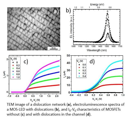
where r is the radius of the cylinder. With r → 0, it follows that the stress components becomes infinite (σxz = σyz →∞). This means that elasticity theory cannot be applied beyond a distance r0, equal to a few atom spacings. This region is defined as dislocation core. Using a typical value of the shear modulus for Si of G = 160 GPa the stress components of a screw dislocation are plotted in Figure 1. There is a long-range stress field around the dislocation. The stress reaches values of about 200 MPa close to the dislocation core (r ≅ r0) and decreases with increasing r. As already mentioned, the stress inside the core cannot be calculated but is estimated to be orders of magnitude higher.
σxx = σyy = σzz = σxy = σyx = 0
The stress field of an edge dislocation is more complex than that of a screw dislocation but can be represented in an isotropic cylinder in a similar way. The displacement in the z direction is zero and the deformation is called plane strain. The stresses are found to be [20]
where
with ν as Poisson’s ratio (ν = 0.22 for silicon). The stress field of an edge dislocation has both dilational and shear components. The largest normal stress is σxx which acts parallel to the slip vector. Since the slip plane can be defined as γ = 0, the maximum compressive stress acts immediately above the slip plane, while the maximum tensile stress acts immediately below the slip plane. Figure 2 shows the stress components for an edge dislocation in silicon. Using typical values for G and ν, the stress close to the core reaches similar values as for a screw dislocation but in different directions.
σxz = σzx = σyz = σzy = 0,
2.2. Two-Dimensional Dislocation Networks
Wafer direct bonding is a smart technique to realize numerous types of two-dimensional dislocation networks under defined and reproducible conditions [34]. A short description of the method is presented in Section 4. Wafer direct bonding requires the adhesion of two semiconductor wafers and a subsequent annealing to modify the atomic bonds via the interface. To generate a two-dimensional dislocation network in the bonded interface, hydrophobic surfaces are required. As a result, two atomic flat surfaces are joined. Because both surfaces are not perfectly aligned to each other, defects are produced during the formation of atomic bonds via the interface in consequence of a subsequent annealing. The defects formed are dislocations in a two-dimensional network strictly located in the interface. The network and type of the dislocations therein depend on the crystal orientation of both initial wafer surfaces, their twist and tilt angles, as well as annealing conditions.
The influence of the crystal orientation of both surfaces is shown in Figure 3. Bonding of two {100}-oriented silicon wafers initiates a dominant dislocation network having square-like meshes produced by two orthogonal sets of screw dislocations. A hexagonal network of screw dislocations is formed if {110}-oriented wafers are applied for the bonding process. Furthermore, a dislocation network with hexagonal meshes is also obtained for bonding of {111}-oriented wafers. Here, the dislocations forming the mesh structure are Shockley partial dislocations having Burgers vectors of the type b = a/6<112>. Bonding of wafers with different orientation has also been investigated. For instance, Bourdell et al. [45] analyzed dislocation networks formed by bonding of (110)- and (100)-oriented wafers. Using the orientation relation <110>{110} parallel to <110>{100}, only parallel arrangements of 60° dislocations are observed. Different results have been found by applying the orientation relation <100>{110} parallel to <110>{100} of analogous wafer pairs [46]. The defects obtained under these conditions are not clearly identified but it is expected that their Burgers vector is about one quarter of a screw dislocation.
The misfit, or the misorientation between both bonded wafers, also influences the morphology of the generated dislocation network. Both the twist and tilt components are directly related to the dislocation distance within the networks. The twist component ϑtwist is related to the dislocation distance Stwist by the equation
while the tilt component ϑtilt is related to the dislocation distance Stilt by
The twist component affects the primary dislocation network, which is the square-like network of screw dislocations in the case of bonding of {100}-oriented wafers. Varying ϑtwist results in changes of the dislocation distance. Decreasing ϑtwist increases the distance of screw dislocations in the network. In reality, the screw dislocation distance is varied from a few nanometers up to a few hundred nanometers.
On the other hand, the tilt component of the misfit causes a second dislocation network overlaying the primary one. This additional network consists of 60° dislocations for bonding of {100}-oriented wafers. Screw and edge dislocations of both networks may react with each other. Different types of interactions are discussed, for instance, in [47] for bonding of {100}-oriented wafers. Interactions between both types of dislocations are only important if ϑtilt ≅ ϑtwist, i.e., dislocation distances in both networks are nearly equal. Because in practical applications mostly ϑtilt << ϑtwist holds, pure screw dislocation networks without interactions with 60° dislocations are observable.
Bonding of wafers with other orientation relations show more complex interactions. The hexagonal network of screw dislocations in the case of bonding of {110}-oriented wafers can also interact with 60° dislocations caused by the tilt component of mistfit. The original (100) twist boundary consists of one set of screw dislocations of the type b = a/2[−110] in the plane and a second set of screw dislocations of the type b = [001] oriented perpendicular [48]. The latter is instable and dissociates according to the reaction
Interaction of both dissociation products with the original screw dislocations in the plane results in
and
Rearrangements of the different segments result in a relaxed arrangement shown in Figure 4 where all segments are parallel to {111}-planes.
2.3. Structure of Individual Dislocations
Transmission electron microscopy is the preferred method to investigate structural properties of individual dislocations. Figure 5 shows a high resolution electron microscope (HREM) image of a cross-section of two dislocations in the interface of a (100)/(100) bonded wafer pair. Caused by the imaging contrast (phase contrast), strain fields around the dislocations are not visible. The dislocations are characterized by distortions of the periodic lattice structure around the defects. The size of the distortion is about one to two nanometer and should define the dislocation core. Weak beam techniques proved an increasing number of dissociated dislocations with increasing annealing temperature [49]. Subsequent annealings after bonding at T ≥ 1050 °C causes that almost all dislocations in the networks are dissociated. A high-angle annular dark field (HAADF) image of a dissociated screw dislocation is shown in Figure 6a. The dissociation causes the formation of two 30° partial dislocations bounding a stacking fault. A model of the atomic structure of the defect is shown in Figure 6c, which corresponds to the structure of a dissociated screw dislocation expected by molecular dynamics [50]. The strain field at the defect is quantified by peak-pairs analysis (PPA) of high-resolution electron microscope images [51]. This method extracts the strain ε in defects and the surrounding area by measurement of the lattice distortion. Analyses of ε in different directions clearly proved the strain fields on the partial dislocations but show also that most of the strain is concentrated on the dislocation cores. Inside the defects, tensile strain of about 10% exists, which is in accordance with theoretical predictions [52,53] and measurements on other dislocations [54]. According to Hooke’s law, a strain value of ε ≅ 10% corresponds to a stress of about 16 GPa, which is more than 100 times larger than in the stress field surrounding the defect (see Section 2.1.). Because it can be assumed that strain affects the band structure of silicon, the exceptionally high strain in dislocation cores detrimentally affects the band structure and therefore the electronic and optical properties.
3. Electronic and Optical Properties of Dislocations in Silicon
3.1. Electrical Measurements on Dislocations
The effect of a dislocation network in the interface of bonded wafers was impressively proved by a simple experiment [55]. Using electron beam induced current (EBIC) technique on a cross-section sample of a bonded wafer pair showed that carriers are transported predominantly along the interface. Measurements of the EBIC contrast indicate a more or less undisturbed transport of minority and majority carriers over long distances.
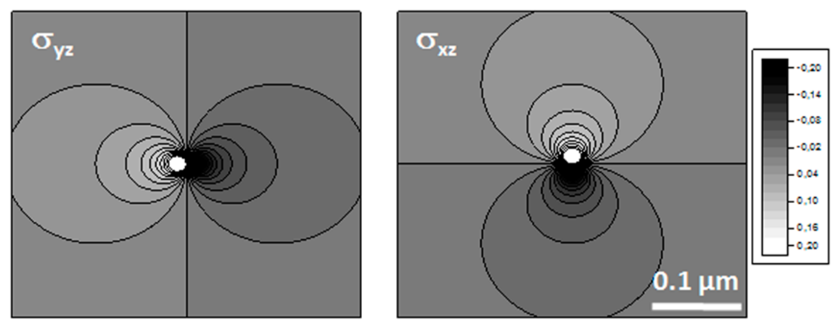
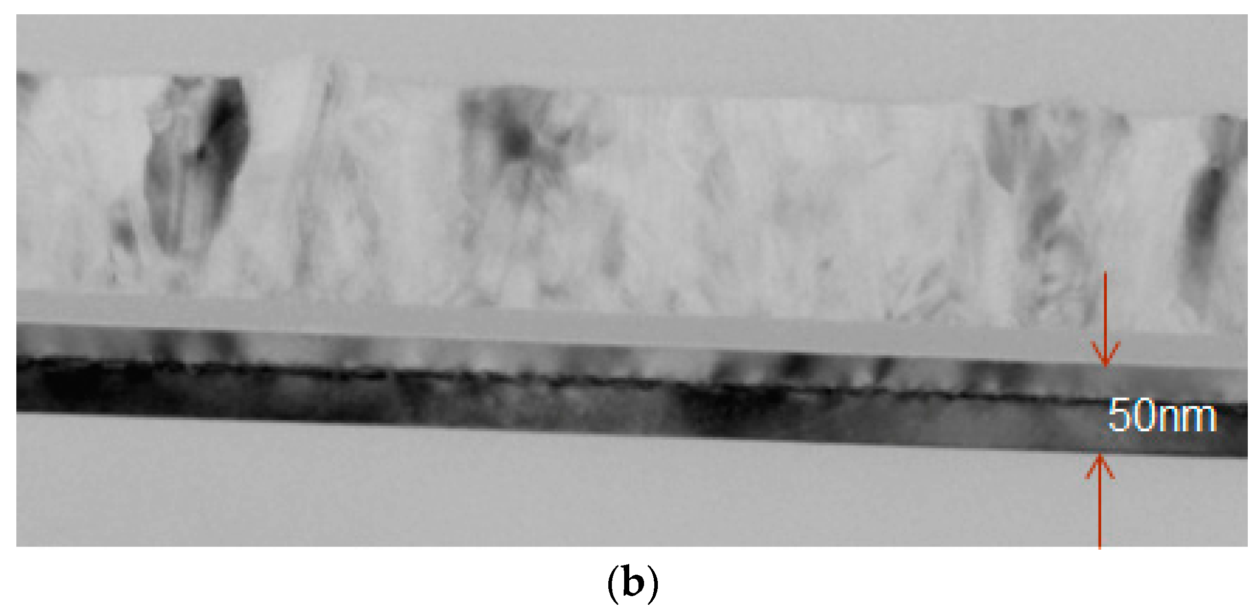
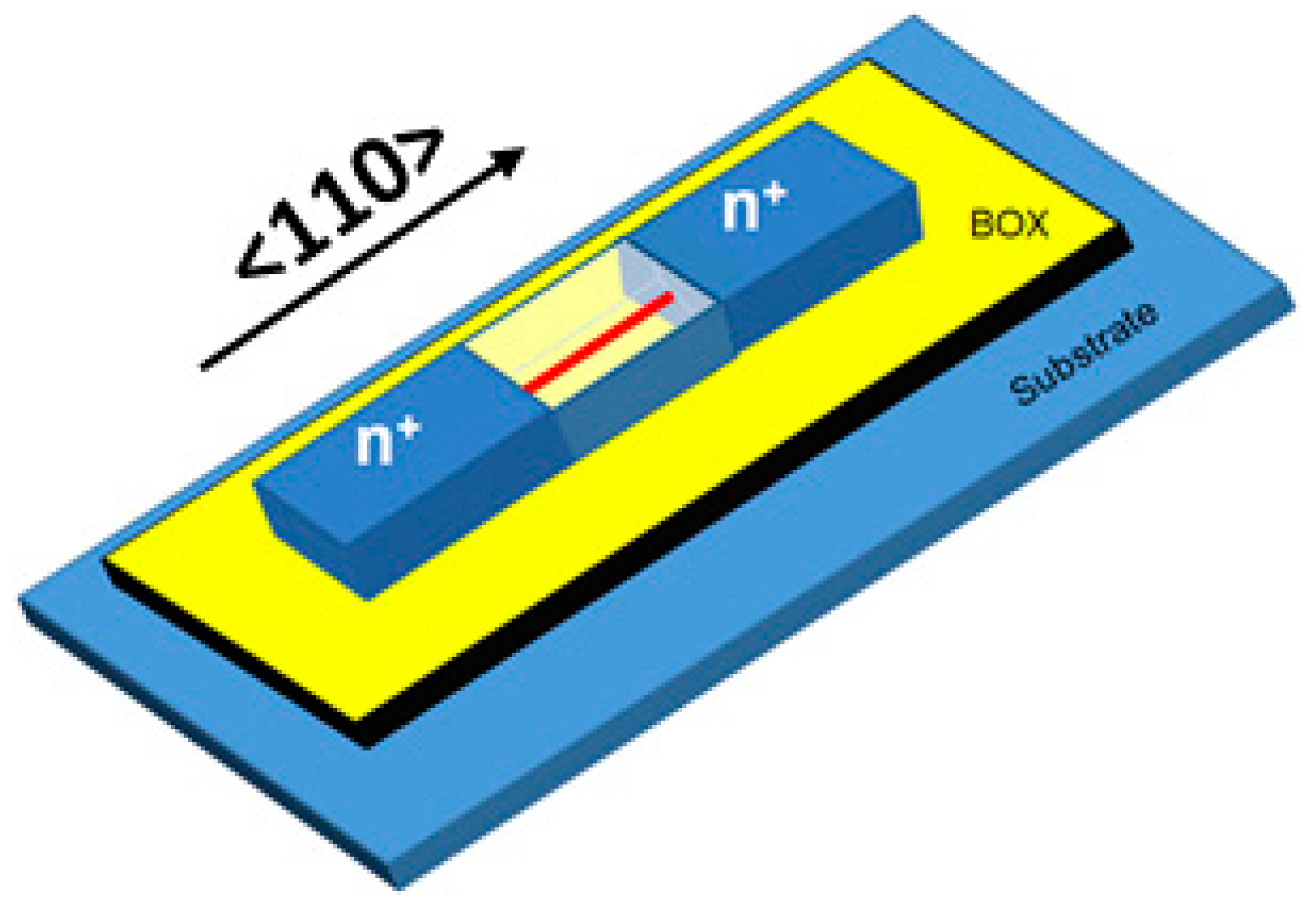
For more detailed measurements on a few or individual dislocations, specific sample preparation techniques and measurement tools are required. To analyze individual defects, one has to exclude possible interactions with defects in the bulk material. This can be done using silicon-on-insulator (SOI) wafers for bonding experiments. Thinning the device layers and subsequent bonding result in new SOI wafers with a dislocation network in a thin silicon layer electrically isolated by a buried oxide (Figure 7a). In the interest of clarity and consistency, here, only results obtained on dislocation networks generated by bonding of (100)/(100) wafer pairs are reported. For measurements of the electronic properties of individual defects, devices are necessary to contact dislocations. Here, MOSFETs are used as test device. Preparing the channel directions parallel to <110>-directions implies that dislocations running parallel to the channel direction. Advantages of MOSFETs are their easy and clean preparation by well-known complementary metal-oxide-semiconductor (CMOS) technologies, a comprehensive knowledge about the device physics, and computer tools to simulate their characteristics. Using n- and pMOSFETs, the transport characteristics of electrons and holes via dislocations were measured. Furthermore, varying the channel width results in varying numbers of dislocations measured. In addition, reference devices without dislocation networks were prepared in the same process runs enabling us clearly to extract the effect of dislocations on MOSFET characteristics. Figure 7b shows a part of the gate complex of a nMOSFET having a dislocation network in the thin (about 50 nm thick) gate electrode.
This section is focused on results of measurements on nMOSFETs, i.e., the transport properties of electrons along dislocations are described in detail. The transport properties of holes are presented elsewhere [56]. Typical output and transfer characteristics are obtained for the reference sample without dislocations (Figure 8a,b). The devices are characterized by a subthreshold slope S = 100 mV/dec. and a threshold voltage VT = −150 mV. The output and transfer characteristics of a device with a dislocation network in the channel are shown in Figure 8c,d. It can be seen that higher drain currents (ID) are measured at the same gate (VG) and drain (VD) voltages, compared to devices without a dislocation network. The increase of the drain current even at very low gate voltages is about one order of magnitude. Similar results were also obtained by other authors [57] and are ascribed to the presence of dislocations. The relatively high source-drain current even at VG = 0 V, in contrast to the reference sample, indicates the presence of charged carriers on dislocations.
Analyses of the device data clearly proved that the number of dislocations in the channel characteristically influences the device parameter. Indications are found by measurements on devices prepared on wafers having dislocation networks with different dislocation density. Such networks are realized by varying the twist angle during the wafer bonding process. Besides devices prepared on a dislocation network with αtwist = 0.31° (resulting in a dislocation spacing of about 15 nm), analogous samples were prepared on a wafer having a dislocation network characterized by αtwist = 0.035°. Here, the dislocation spacing is about 150 nm. Using channel widths W between 1 μm and 10 μm, devices having about 660 dislocations (at a dislocation spacing of 15 nm and W = 10 μm), up to six dislocations per channel at a dislocation spacing of 150 nm and W = 1 μm were prepared. The ID–VD curves of these devices show that the drain current depends on the number of dislocations in the channel. At VD = 2 V, a drain current of 3 × 10⁻³ A is obtained if there are only six dislocations in the channel. On the other hand, a value of ID = 2 × 10⁻⁶ A is measured under the same conditions if the channel includes about 660 dislocations. If the drain current is plotted as a function of the number of dislocations, a linear relation is obtained [58]. It is shown that the drain current decreases as the number of dislocations in the channel increases. Fitting the data allows one to extrapolate the current given by one dislocation of more than 10−2 A, which corresponds to a current density of more than 1012 A/cm2. The extrapolated value was experimentally verified by measurements on single dislocations [59]. These measurements were realized by reducing the channel width down to about 30 nm by applying electron beam lithography in combination with dry etching. A current density of 3.8 × 10¹² A/cm2 was extracted experimentally, which corresponds to a resistivity for a single dislocation in silicon of ρ ≅ 10−8 Ωcm. This means a supermetallic behavior of dislocations.
Besides the drain current (ID) also the threshold voltage (VT) and the subthreshold swing depend on the dislocation density. Increasing the number of dislocations by a factor of 10, for instance by increasing the channel width from 1 μm to 10 μm, results in a decrease of VT from about −400 mV to −150 mV for nMOSFETs. An explanation could be the dependence of VT and the subthreshold voltage shift (ΔVT) on the effective channel length of MOSFETs [60]. Decreasing the effective channel length results in an increase of ΔVT. If dislocations are present in the channel, the effective channel length is defined by the number of dislocations as the effective transport channels. Therefore, reducing the number of dislocations in the channel result in an increase of VT and ΔVT. Furthermore, an analogous increase of the subthreshold swing is generally interpreted as thickness effect of the device layer for short channel SOI-MOSFETs and is caused by an inhomogeneous electron concentration in the layer [61].
Commercially available TCAD (technology computer aided design) programs are powerful tools to simulate the characteristics of a large number of electronic devices. Here, we used the ATHENA/ATLAS simulation package (Silvaco) [62], which supports two- and three-dimensional device simulations. Because dislocations represent conductive channels, they are assumed as thin n-type layers embedded in the 80 nm thick channel of a nMOSFET. The ID-VD- and ID-VG characteristics are calculated and compared with the experimentally measured ones by fitting the donor concentration in this thin layer. It was shown that a donor concentration of 3 × 1018 cm−3 in the thin layer results in an increase of ID by one order of magnitude as proved by experimental measurements. This is caused by the formation of a conductive channel along the thin (dislocation) layer already at very low drain and gate voltages [62]. The reference transistor without dislocations, however, is characterized by an electron concentration more than one order of magnitude lower. A conductive channel is not formed under these conditions. Since the donor concentration is equal the electron concentration, the number of electrons in the 2 nm thick layer is estimated to be 6000 for W = L = 1 µm. Furthermore, the behavior of the subthreshold slope refers to an inhomogeneous electron concentration [58] which suggests that all electrons are bounded to dislocations. TEM investigations revealed that there are 30 dislocations in the channel for this specific case, which means about 200 electrons per micrometer dislocation length. This corresponds to the maximum number of electrons on a dislocation [63]. Assuming a homogeneous distribution along the dislocation line, the distance between free electrons on the dislocation core is about 5 nm. There is no evidence about the locations of electrons on the dislocation core. The distance of about 5 nm is significantly smaller than the distance of dislocation nodes in the network (about 30 nm in this case) and means that electrons are located on straight dislocation segments. Moreover, kinks on dislocations could be a promising candidate. However, only narrow kink-kink distances of about d ≅ 2b ≅ 1.6 nm are stable. Here, b is the length of the Burgers vector. Larger kink-kink distances up to d ≅ 10b were calculated but it was shown that such wide kinks are intermediate states only. Therefore metallic conduction along dislocation lines in the p-type material is assumed in accordance with results described above and conclusions of other authors [64]. It is caused by a two-dimensional carrier confinement along dislocations.
Furthermore, simulation tools enable us also to analyze the temperature dependence of device characteristics of MOSFETs containing dislocations. Figure 9a shows the measured and calculated transconductance gm of devices without (reference) and with dislocations (type A) as a function of inverse temperature. The type A dislocations are from a pure screw dislocation network. Measurements of the twist angle of the network (ϑtwist = 1.45°) refer to 77 dislocations in the specific device channel.
The behavior of gm is simulated for the reference sample without dislocations by considering Klaassen’s unified mobility model [62,65] (open symbols, Figure 9a). The decrease of gm with decreasing temperature measured for devices with dislocations of type A can be only understood by assuming an additional temperature-dependent incomplete ionization of carriers [66]. This means a partial freeze out of carriers on dislocations with decreasing temperature if gm is below the corresponding value of the reference sample. If all these assumptions are taken into account, the temperature dependence of the electron concentration can be calculated and compared to experimental data. Figure 9b shows that mixed dislocations in the channel (type B) result in a two orders of magnitude higher electron concentration in the channel at T = 80 K compared to reference devices without dislocations. Devices containing screw dislocations, however, result in an electron density about one order of magnitude lower at the same temperature. The high concentration of excess carriers is the reason that MOSFETs with mixed dislocations in the channel operate also at very low temperatures. A low subthreshold swing of SS = 21 mV/dec was measured at T = 5 K [65].
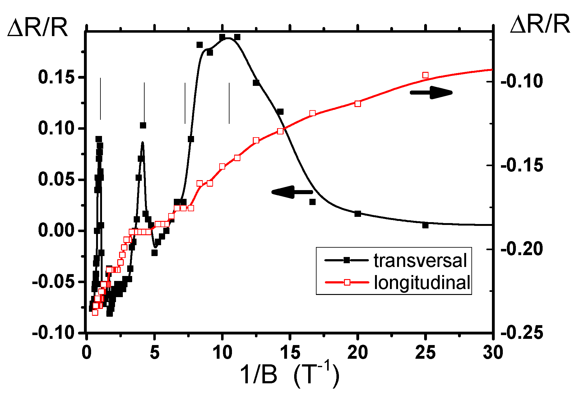
Indications to the carrier confinement along dislocations result from further measurements at extremely low temperatures and by applying external magnetic fields [56,62,67]. Magnetoresistance measurements, for instance, revealed Shubnikov–de Haas (SdH) oscillations indicating the presence of a two-dimensional electron gas (2DEG) on dislocation networks in p-type silicon (Figure 10). The asymmetry of the SdH oscillations is frequently observed, but different reasons are discussed [68]. Because dislocations represent nanowires, the asymmetry may be attributed to the fact that field-dependent oscillations are extremely sensitive to the alignment between field and wire axis.
Analyses of SdH oscillations yield details about the properties of the 2DEG. At low temperatures and weak magnetic fields, SdH oscillations are described by the equation [68]
where σxx is the in-plane conductivity, F(°)(E) and F(1)(E) are slowly varying functions of the energy E, kB is Boltzmann’s constant, T is temperature, µ is the chemical potential, ħ is the reduced Planck constant, and ωC is the cyclotron angular frequency (ωC = eB/mc). B is the magnetic field, e is the magnitude of electronic charge, m is the effective mass, and c is the velocity of light. In the presence of strong magnetic fields, equation
holds [68], where Ns means the electron concentration, and τq is the relaxation lifetime.
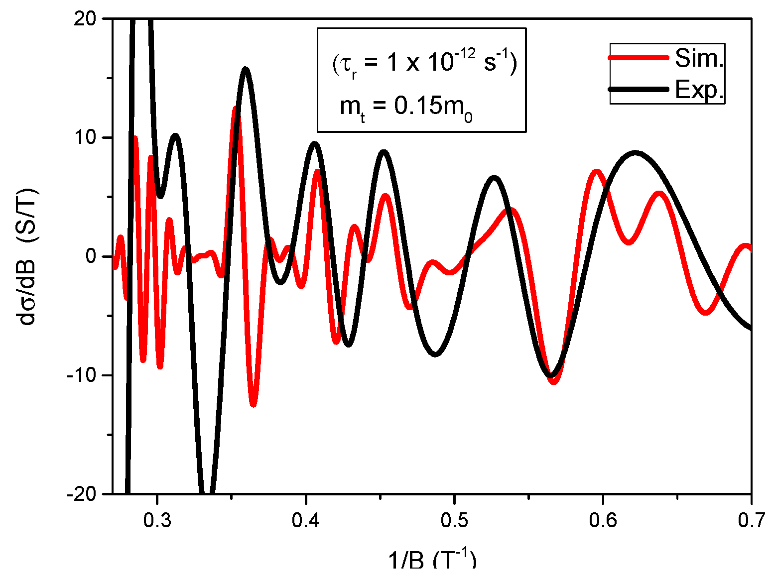
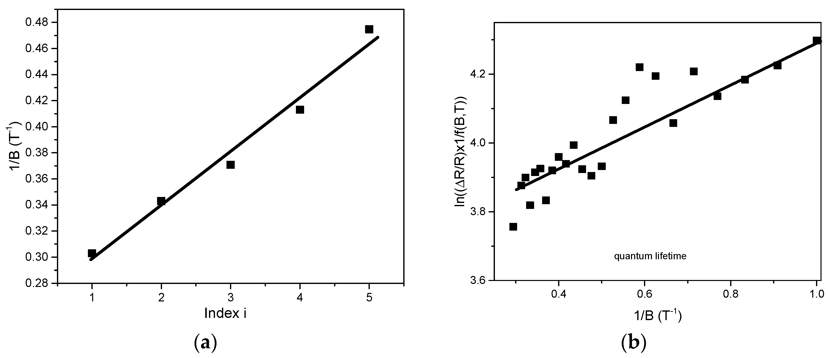
For simulation of experimental data, Equation (13) is used for B ≤ 10 T. Figure 11 shows an example of experimentally measured SdH oscillations and calculated data using Ns = 4.1 × 1012 cm−2 and τq = 6 × 10⁻¹² s−1. A sufficient agreement is obtained. Differences are caused by the experimental procedure. Only a limited number of data points can be measured (ΔB = 250 mT) in order to ensure stabile thermal conditions at this low temperature over a long time. The fit parameter Ns and τq are determined from experimental data using procedures described elsewhere [69]. Plotting the measured values of vs. the index i (the number of a oscillation) gives a straight line with the slope given by 2Ns/hn. Here, n is the quantum number and h Planck’s constant. Figure 12a shows the plot of these quantities resulting in an electron concentration of Ns = 4.1 × 1012 cm−2.
Furthermore, the quantum lifetime τq is calculated from plots of the quantity
vs. 1/B, where f(B,T) is a temperature-dependent function [69] and mt is the transversal effective mass. Values of τq are extracted from the slope of the resulting straight line (Figure 12b). The effective mass has been also determined from temperature-dependent measurement as mt = 0.15 m0. The value of mt is slightly lower than the generally accepted value for silicon (mt = 0.19 m0) which may be caused by electron–electron interactions as a consequence of the higher electron concentration in the electron gas [68]. However, it is important to remember that band structure calculations, discussed in the next section, result in the same value of mt = 0.15 m0 if the high strain in the dislocation core is taken into account.
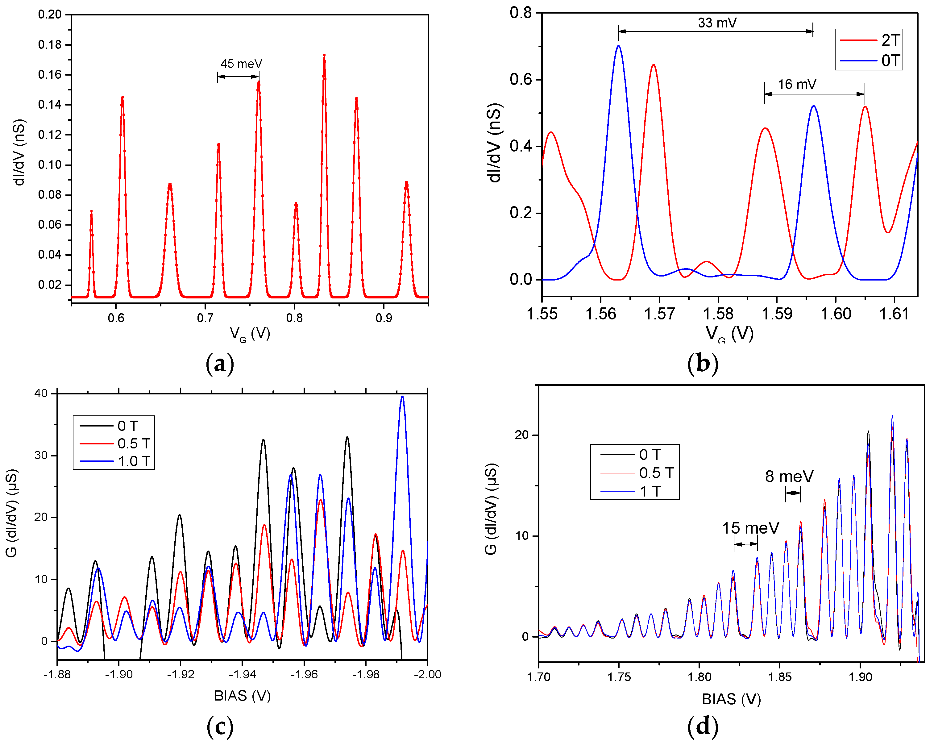
As a consequence of the 2DEG, single-electron transitions (Coulomb blockades) are observed for nMOSFETs containing dislocations in the channel [67]. Figure 13 shows an example of equidistant oscillations in VG, which is typical for a single-island system where each peak corresponds to the addition of one extra electron onto the island. The current-voltage (ID–VD) characteristic refers to a non-ohmic semiconductor-like behavior with zero conductivity in the low voltage limit at T = 0.3 K. The period (ΔVG) of the oscillations is about 45 mV (Figure 13a) resulting in a gate capacitance CG = e/ΔVG = 3.5 aF. Variations of the amplitude indicate the quantum regime, which can be also deduced from temperature-dependent measurements. Plots of full-width-half-maximum (FWHM) of the peak width vs. increasing temperature yields a linear dependence with a slope of the curve equal to 3.5 kT [70]. Furthermore, a conversion factor [71] is extracted from temperature-dependent measurements, resulting in an energy level spacing between discrete states along the wire axis ΔE = α/ΔVGS = 10 meV, which is close to data reported from grown silicon nanowires [72].
Further information about Coulomb blockades are obtained by applying external magnetic fields parallel to the dislocation plane [67]. Especially, peak splitting is observed, which linearly increases with increasing strength of the magnetic field. At B = 2T, the peak splitting is about ± 8 mV (Figure 13b) which is more than 10 times larger than the Zeeman splitting given by the equation
Using g* = 2, the effective g factor, and µB = 9.27 × 10 −24 J/T, the Bohr magneton, ΔEZeeman = 115 µeV/T follows. Therefore the large peak splitting has other reasons. It is shown further on that strain-enhanced valley splitting is a main reason.
The periodicity and amplitude of the Coulomb blockade oscillations depends on the dislocation type and on the number of parallel dislocations in the device channel. Increasing the number of dislocations increases not only the period of the Coulomb blockade oscillations but also their amplitude. Both refer to interactions between the quantum dots on different dislocations [67]. On the other hand, Coulomb blockades as shown in Figure 13a have been typically observed for screw dislocations. Mixed dislocations, i.e., dislocations having not only screw but also edge components, are characterized by a different behavior. Using, for instance a diode structure, Coulomb blockades are observed by applying a positive or negative bias (Figure 13c,d). This indicates single-electron and single-hole transitions on the same dislocations.
3.2. Comparison with Theory
Dislocations change locally the translational symmetry of a crystal resulting in modifications of the band structure. Based on early experiments to the plastic deformation of highly doped p-type germanium [73,74], Read [75,76] concluded that edge dislocations induce an acceptor level in the band gap. This would mean that dislocations are negatively charged. The line charge of the dislocation is electrically screened in Read’s model by ionized donors in a surrounding cylinder. Free electrons cannot penetrate the cylinder and will be reflected on his surface. Such a dislocation appears neutral in an outward direction and causes an energy level about 0.2 eV below the conduction band [75]. The described model was not confirmed by further experiments on lower doped p-type Ge and Si [77,78]. Schröter and Labusch concluded from their investigations that dislocations may act as both acceptor and donor [26]. The opposing models of Read on the one hand and Schröter and Labusch on the other hand were combined by Veth and Lannoo [79]. These authors introduced an additional intra-atomic Coulomb term J, carried out a self-consistent calculation of the potential close to a dislocation, and assume the classical screening outside the dislocation core according to Read. Based on these conditions, the shift of a dislocation-induced energy level Ee close to the valence band edge is, for instance, calculated using the equation
where in p means the number of excess electrons per atom, εdi is the dielectric constant, a is the atomic distance inside the dislocation core, e is the elementary charge, and R is the radius of the screening space charge cylinder given by the equation
with ND and NA as donor and acceptor concentrations, respectively. From Equation (17) follows a linear dependence of Ee on p, which is in agreement with the model of Read and the linear charge model of Schröter and Labusch [79].
Both models about the electrical activity suppose the screening of charges along the dislocation core by opposite charges in a surrounding cylinder. This would mean that dislocations in n-type silicon or germanium are characterized by a negative line charge along the dislocation core surrounded by a cylinder of ionized (positively charged) donor atoms. In the opposite case of p-type material, a dislocation possess positively charges along the core surrounded by ionized (negatively charged) acceptor atoms. This interpretation, however, is in contrast to electrical measurements described in the previous section and elsewhere [56,62,80], namely,
- (i.)
- An increase in the drain current for nMOSFETs results from an increased electron transport along dislocations in the device channel. Note that the channel material is p-type silicon for nMOSFETs.
- (ii.)
- An increase in the drain current also exists for pMOSFETs, where holes are involved in the carrier transport. The channel material here is n-type silicon.
- (iii.)
- There are dislocations (mixed dislocations) that may transport electrons and holes in the same time.
- (iv.)
- Measurements at very low temperatures (T < 1 K) proved the functionality of MOSFETs having dislocations in the channel. Ionized impurity atoms in the surrounding cylinder screening the line charge of the dislocation core, would be completely froze out at this extremely low temperatures. Then, according to the models of Read and Schröter and Labusch, only a line charge of the same type as the bulk material remains. Note that reference devices without dislocations in the channel do not operate at such temperatures.
- (v.)
- It would be also conceivable that, supposing the charges on the dislocation core are bounded to atoms, they are increasingly immobile at very low temperatures. This, however, is in contrast to the obvious facts of the MOSFET functionality at T < 1 K and the supermetallic behavior at higher temperatures.
One decisive reason for the described contradictions is measurements on dislocations produced under different experimental conditions. Plastic deformation used in the work of Read and Schröter and Labusch results in large numbers of dislocations and high densities of other defects (especially point defects), which, depending on the experimental conditions, react with each other. For measurements, bulk type samples were also necessary, which could lead to a further increase of reactions with other defects. On the other hand, here we used defined numbers and types of dislocations, resp., embedded in a thin silicon layer electrically isolated from the bulk of a wafer. Interactions with other defects (point defects and impurities) can be excluded. The application of MOSFETs as test vehicles enables us also to form direct electrical contacts on the dislocations. Furthermore, combining electrical measurements with electron microscope methods on the same samples results in structural and electrical properties about individual dislocations in the same time.
Our interpretation about the electrical activity of dislocations based on the following facts:
- (i.)
- Dislocations are characterized by dimensions of a few nanometers in diameter and up to a few micrometers in length. This means that dislocations are native nanostructures embedded in a crystalline matrix and therefore quantum mechanical effects play an important role for interpretation of their electronic properties.
- (ii.)
- Low-temperature measurements proved a two-dimensional electron gas (2DEG) for samples containing a dislocation network. The 2DEG of the network consists of a number of one-dimensional electron gases (1DEGs) on individual dislocations.
- (iii.)
- The electron gas is the reason for the supermetallic behavior and makes it possible that MOSFETs operate at extremely low temperatures.
- (iv.)
- Electron microscopy proved high strain levels on the core of dislocations. The strain is in the order of 10% (ε ≅ 0.1) corresponding to a stress of σ ≅ 16 GPa. Such values are about two orders of magnitude higher than in the long-range stress field around the defect. The stress is uniaxial tensile in the case of screw dislocations and compressive for edge dislocations.
The effect of different types of strain (uniaxial, biaxial, tensile, and compressive) on the band structure of Si and device properties has been analyzed using different simulation techniques [81,82,83,84,85,86].
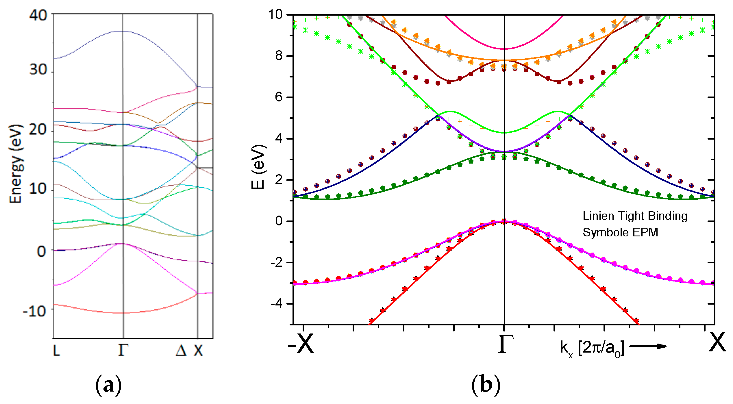
All simulations of the band structure, reported here, were performed by applying the nextnano3 simulation package [87]. The bulk band structure was calculated using both a 6- and 8-band k∙p model as well as an empirical sp3d5s* tight binding model [88] taking into account strain and deformation potentials. Results of these calculation were supported by simulations using the empirical pseudopotential method (EPM) [89]. The EPM program package used here is described in [90]. Figure 14a shows the calculated band structure of silicon using the tight binding method. For comparison, a part of the band structure along <100>-directions is shown in Figure 14b calculated using tight binding and EPM methods, respectively. This demonstrates that both simulation methods deliver consistent results.
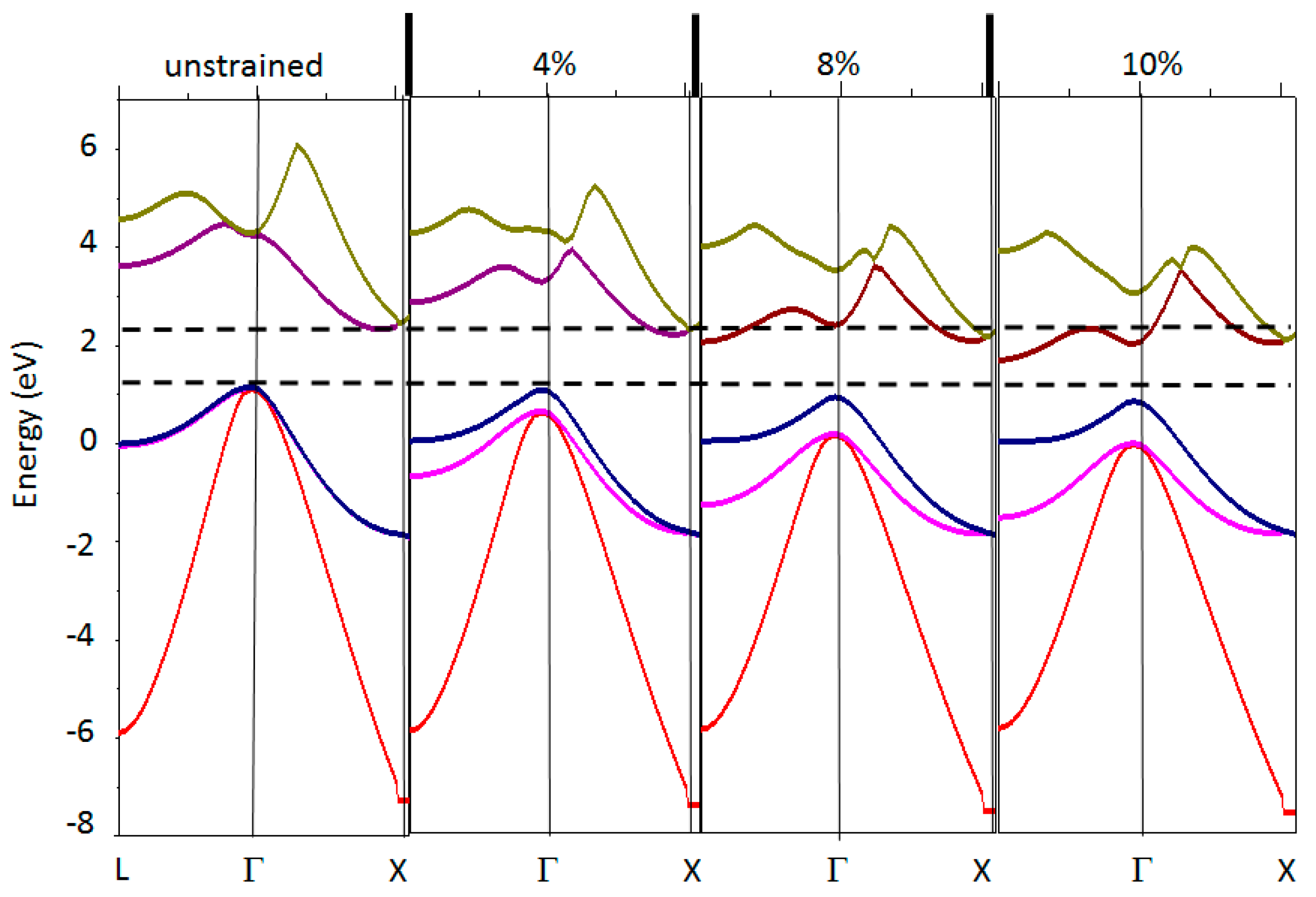
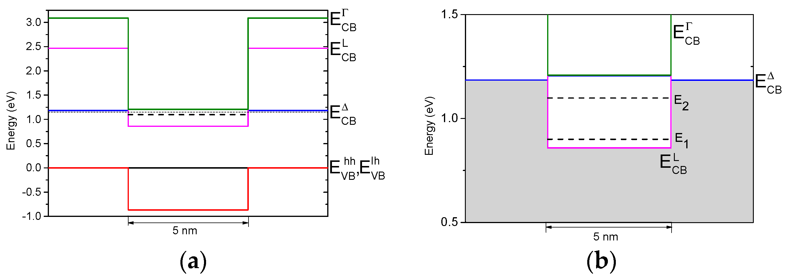
A nMOSFET with a dislocation extended from source to drain in the center of the channel is the principal structure for our investigations. The channel direction and therefore the direction of the dislocation line is <110>. This introduces uniaxial tensile strain parallel to the channel direction if a screw dislocation is assumed. Band structure calculations revealed shifts of the conduction and valence bands at the Γ- and L points as well as band warping with increasing tensile strain (Figure 15). The position of the upper valence band Ev,hh (synonymous with the heavy hole (hh) and light hole (lh) bands) decreases continuously with increasing strain. At ε = +0.1 (10% tensile strain), the reduction is ΔEv,hh = −0.818 eV. Increasing tensile strain increases simultaneously the splitting of the heavy hole (hh) and light hole (lh) bands reaching about Ev,hh − Ev,lh = 0.891 eV at ε = +0.1.
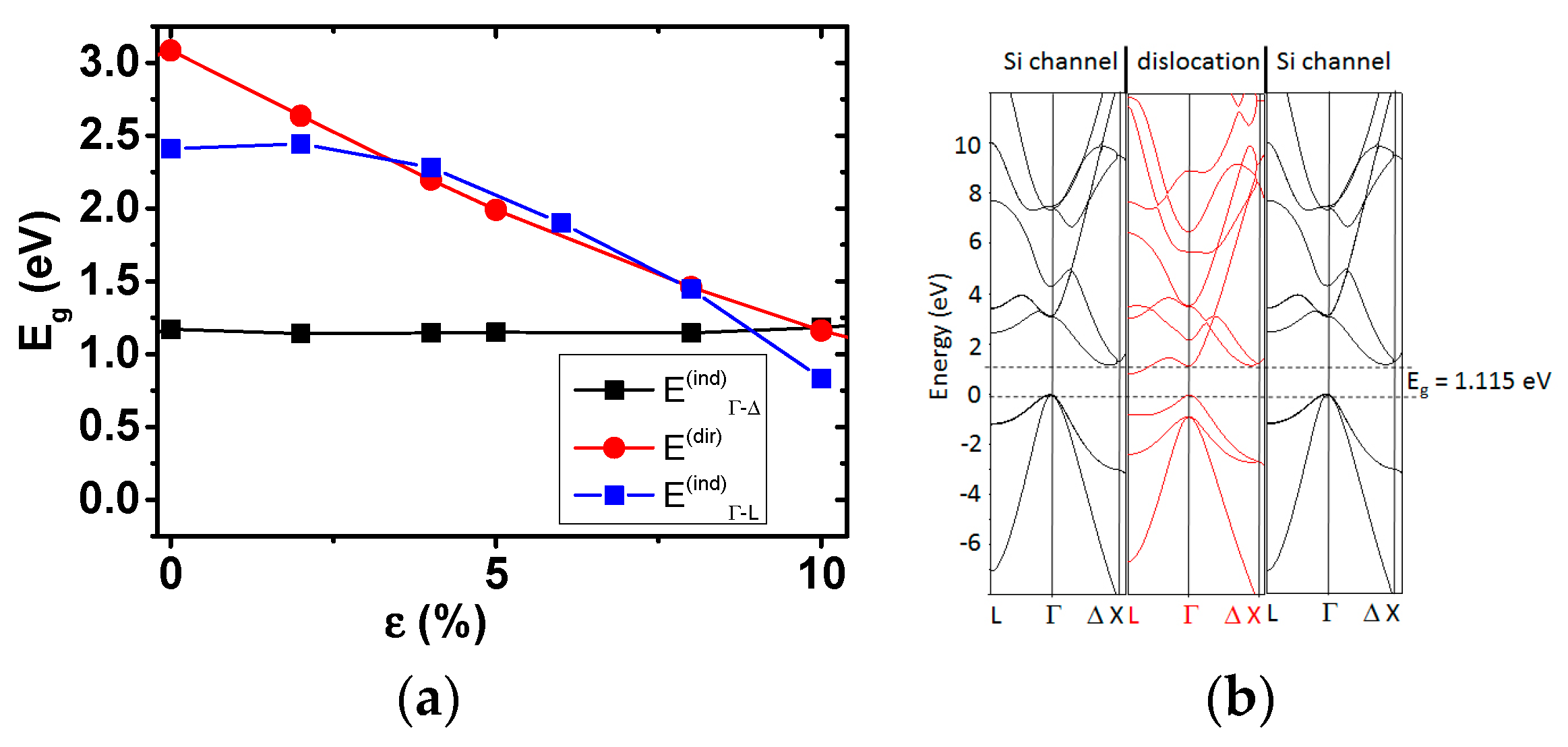
There are only slight variations of the conduction band minimum at Δ with increasing tensile strain. If ε = +0.1, the lowest conduction band at the Γ point () is equal to the position of the lowest conduction band at Δ of the unstrained Si (Figure 16a). As a result, the band gap energies of the indirect and direct transitions are equal for such high tensile strain and Si changes from the indirect into a direct semiconductor [80]. This conclusion is in agreement with previously reported data [85,86]. Furthermore, the shift of the conduction band minimum at the L point results in an additional indirect transition in the presence of high tensile strain. The band gap at this new indirect transition is = 0.832 eV at ε = +0.1 and therefore smaller than the original indirect and direct band gaps , respectively. Similar data have also been published for nanowires, where, however, the absolute data depend on the wire diameter [85]. The variation of all band gaps with increasing tensile strain is summarized in Figure 16a. Using the model of a dislocation surrounded by unstrained silicon, a schema of the band structure as in Figure 16b follows. The shifts of the conduction band of the strained dislocation core result in one or more one-dimensional defect bands in the band gap of the surrounding Si channel. The depth of the defect bands increases as the tensile strain increases. Compressive strain, on the other hand, results in a dominant shift of the lowest conduction band at Δ (). This induces a one-dimensional defect band about 300 meV below the conduction band at moderate compressive strain (ε ≤ −0.04). Further increase of the dislocation-induced strain increases and causes the formation of a one-dimensional defect band close to the valence band if ε < −0.08.
The dependence of the effective masses of electrons and holes have been calculated from energy dispersion curves using
in the close vicinity of the band extremum [86]. The calculated hole mass mh = 0.285 is almost constant if strain is varied between −0.1 ≤ ε ≤ +0.1 and corresponds to previously published data [86]. The effective in-plane electron mass parallel to the strain direction (meff) decreases continuously with increasing tensile strain and is mt = 0.15m0 at ε = +0.1. This is exactly the same value of the effective mass extracted from measurements of the SdH oscillations described in Section 3.1. The decrease of effective mass even at higher tensile strain is much less than predicted from measurements at lower tensile strain (ε ≤ +0.01) [83,91].
Summarizing all results achieved from band structure calculations leads to the following conclusions. Tensile strain induced by a dislocation shifts locally both, the valence and conduction bands causing an additional indirect transition between the valence band at Γ and the conduction band at L as well as the direct transition at the Γ-point. A cross-section through a dislocation yields a quantum well shown in Figure 17. Data from band structure calculations indicate the lowering of the minimum of the lowest conduction band at the L-point () below that at Δ of the unstrained Si (). At the same time, the valence band maximum of light and heavy holes are also shifted downwards. For p-type silicon, discussed here, changes of the conduction band are most important (Figure 17b).
The interpretation of dislocations as quantum wires explains most of the experimental results. The presence of SdH oscillations refers to a 2DEG if two-dimensional dislocation networks exist in the channel of MOSFETs. Because a network is formed by periodically spaced dislocations, the 2DEG represents a two-dimensional set of one-dimensional electron gases (1DEG). Moreover, the energy quantization is related to the presence of Coulomb blockades proved by low-temperature measurements. The model of dislocations as quantum wires bears similarities to the previously published shallow band model, which, however, assumes 1D-bands about 50 to 100 meV below the conduction and above the valence band, respectively [92,93]. Deeper defect-induced states of minority or majority carriers proved by DLTS [94,95,96] are not considered therein, but are explainable on the basis of the quantum wire model. If atomic defects on the dislocation core are taken into account (kinks, jogs, etc. [19]) then local changes of strain along the dislocation line exist modifying locally the band structure and consequently the quantum wire. Therefore, a broad defect line appears in the DLTS spectrum.
An analogous discussion of the formation of quantum wells by dislocation-induced compressive strain also appears possible, which, however, is based on the primary indirect transition between Γ and Δ [56].
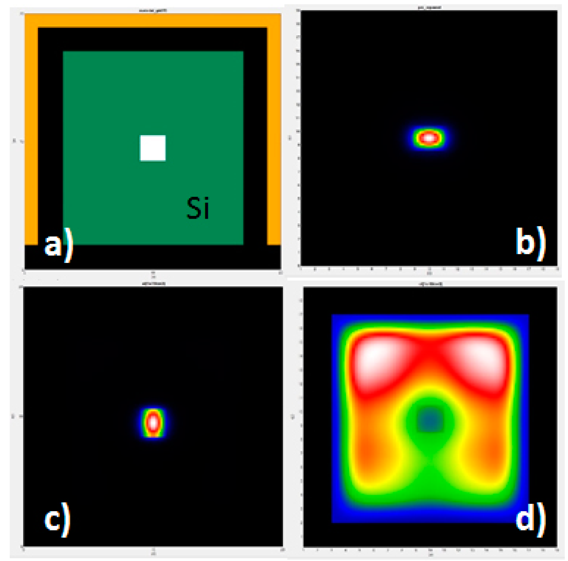
Furthermore, the effect of the dislocation-induced carrier confinement on the MOSFET characteristics is also explainable. In order to do this, a two-dimensional quantum mechanical device simulation package (nextnano3) was applied allowing the self-consistent solution of the two-dimensional Poisson, Schrödinger, and current equations. The device used for simulation is schematically shown in Figure 18a. An unstrained silicon channel (20 nm × 20 nm) is supposed. A dislocation is assumed as a square of 2 nm × 2 nm in the center of the channel. Adapting the modified band parameters resulting from a uniaxial tensile strained dislocation (ε = +0.1) cause a localization of the first wave function inside the dislocation (Figure 18b). This leads to the highest electron concentration inside the dislocation (Figure 18c) and therefore to the dominant current flow through the defect. On the other hand, the highest electron density is close to the gate if an unstrained silicon channel without a dislocation is used (Figure 18d). Note that a preferred current flow through the dislocation is only obtained by the carrier confinement because of band alignment induced by the high uniaxial strain. Mobility enhancement only by reduced effective masses is not the primary reason.
3.3. Optical Properties of Dislocations—Electron-Hole Recombination at Dislocations
The D-band luminescence is a result of radiative electron-hole recombination via dislocation-related electronic states in Si (see below). The efficiency of luminescence is determined by competition of radiative and non-radiative recombination.
The most used experimental tools for probing the carrier recombination at dislocations are the measurement of minority-carrier lifetime (or diffusion length) in case of high dislocation density and electron-beam-induced current (EBIC) or light-beam-induced current (LBIC) in case of small dislocation density. The EBIC and LBIC technique are unique among the electrical characterization methods with respect to a spatial resolution, sufficient to analyze single dislocations. In EBIC or LBIC, the variation of the current at a Schottky contact resulting from excess electrons and holes generated locally by the electron or light beam, is measured, when the specimen area of interest is scanned. The values of current at the dislocation, Idisl, and away from it, I0, are used to define the contrast Cdisl = (I0 − Idisl)/I0 of single dislocations. The Cdisl is proportional to the recombination rate Rrec of minority carriers at a given dislocation [97].
Numerous experimental investigations (see for example [98,99,100,101,102,103]) show that dislocations in different Si samples often exhibit very different EBIC contrast behavior Cdisl(T). This is illustrated in Figure 18a showing typical examples of Cdisl(T) measured for dislocations in different samples, but at similar experimental conditions. Such a big difference in recombination rates at dislocations in different samples correlate with the fact, known also from DLTS, that dislocations in different samples have very different concentration of deep intrinsic core defects and deep (metal) impurities.
Good quantitative explanation of experimental results is possible in a model [104], which differs from earlier model [105] in including electronic transitions between 1D-bands EDe, EDh and deep localized states EDD due to overlapping of their wave functions, see recombination paths (3) in Figure 14b. Taking these transitions into consideration was found to be really essential for a proper description of the dislocation recombination activity.
The recombination rate (1) by transition between 1D-bands is relatively slow. Thus, the recombination activity of “clean” dislocation is small (compare behavior-1 in Figure 19a). However, the recombination can be drastically enhanced by the presence of even small concentration of impurity atoms or core defects at dislocation. In this case it occurs in several steps: capture of free electrons and holes to 1D-bands, their motion along dislocation, then capture from the 1D bands to deep states of defects and recombination. The model allows not only explaining experimentally observed dependencies of recombination rate on temperature and excitation level, but also estimating the concentration of deep level defects at dislocations.
“Clean” dislocations exhibit only very weak recombination activity with a maximum at about 50 K and untraceable activity at room temperature, denoted by type-1 in Figure 19a. Weak contamination (104–105 deep impurities per cm dislocation length) leads to an increase of the activity, still leaving the room temperature activity below detection, denoted by type-2 in Figure 19a. Combination of EBIC and DLTS indicates that for such a small concentration the impurities are attached to the dislocation core [106]. Upon further increase of contamination, the type of the temperature dependence changes and the recombination activity is detected at room temperature, see types-3 and -4 in Figure 19a. Appearance of type-4 requires more than 106–107 deep impurities per cm dislocation length. Now, the impurities are accommodated in the dislocation strain field. Experiments with hydrogenation and phosphorus diffusion gettering have shown that both treatments change the c(T) behavior in a reverse sequence from type-4 to type-2, which represents the lower limit. This limit results from the fact that the impurities accommodated in the dislocation strain field can be passivated by hydrogenation or removed by external gettering, respectively, but the impurities attached to the dislocation core cannot be affected or removed [106,107].
The dislocation-related luminescence in Si consists of a quartet of four broadened lines (or bands), D1 to D4, which was revealed for the first time by Drozdov et al. [28,29]. Figure 20 shows a typical D-band spectrum formed by dislocations in Si. Even though many experiments were carried out over more than a quarter of century, the origin of the D-bands is still not yet completely understood. The current status of the discussion was summarized, for instance, by Kveder and Kittler [63].
Nevertheless, it is widely accepted that D4 and D3 form a pair. The good coincidence between the energy of D4 line and the energy difference EDe–EDh (see Figure 19b) suggests that the D4 line corresponds to no-phonon recombination of electrons in 1D band EDe with holes in 1D band EDh. The D3 line is most probably a TO phonon replica of D4. The D1-line is probably formed by the transition between one of the shallow 1D-bands (EDe, EDh) and a deeper state, compare e.g. [108,109]. The origin of the D2-line is still under discussion. There are indications that D1 and D2 are not a pair.
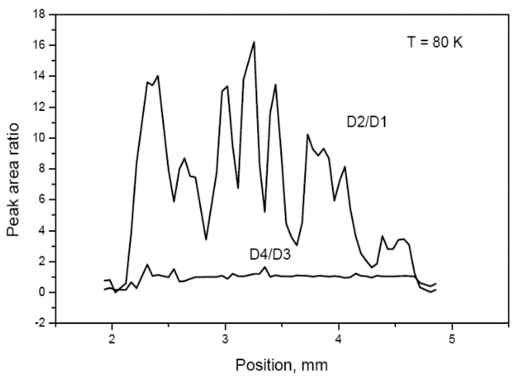
Investigation of multi-crystalline Si, used for solar cells, allows one to analyze the relation between the intensity of different D bands. As the local density of the dislocations varies in this material from point to point, one can expect also variations in the intensity of the D lines. Profiles of the intensity of the D lines were measured over a distance of a few mm. Figure 21 shows the corresponding ratios D2/D1 and D4/D3. The intensity ratio of D4/D3 was found to be nearly constant. On the contrary, the D2/D1 ratio scattered strongly [110]. This observation confirms that the lines D3 and D4 have the same origin, while the lines D1 and D2 are not a pair but have different origin.
Often, very distinct energetic positions are indicated for the D-lines, e.g., D1 = 0.812 eV, D2 = 0.875 eV, D3 = 0.934 eV, and D4 = 1.000 eV at T = 4.2 K. However, their exact energetic positions are found to depend on temperature, electric field [111], elastic strain [112], etc. Figure 22 shows for the D1-line a 30 meV wide domain in which this line may fall. For more details see [113].
It is also noteworthy that the D-line intensity was observed to be affected by the contamination of dislocations with metal impurities. Higgs et al. [114] reported a strong dependence of the D1- and D2-line intensity on the contamination of dislocations with copper which was controllably introduced from the sample surface. For “clean” dislocations, very small luminescence close to the detection limit was observed and for dislocations with very strong contamination a very small intensity was found, too. However, for a low/medium level of Cu contamination the D-line intensity was significantly enhanced. A maximum intensity was reached for a certain low level of Cu contamination.
The evolution of the D-band luminescence has been also obtained on two-dimensional dislocation networks formed by wafer bonding. Photoluminescence, cathodoluminescence, and electroluminescence were applied for these studies (for instance [55,115,116]). All investigations proved a typical dependence of the resulting luminescence spectra on the type and distance of dislocations (or dislocation density) in the network. This is illustrated in Figure 23 where photoluminescence spectra of samples containing two different dislocation networks are shown. Smaller twist angles (i.e., larger dislocation distances) result in an increase of the luminescence at 1.5 µm (D1), while larger twist angles (i.e., shorter dislocation distances) increase the luminescence at 1.3 µm (D3). Another factor influencing the resulting luminescence is the type of dislocations forming the network. So-called mixed dislocations were identified in particular as most important for radiative recombination.
Silicon photonics will be essential for future integrated circuits. Many key components that can be integrated on the chip have already been demonstrated by Si technology. However, a CMOS-compatible light emitter is still lacking. The desired emission wavelength must be >1.1 μm to prevent absorption within Si waveguides. Accordingly, dislocation-based D-line luminescence can be used to integrate novel all-silicon light emitters. Here we discuss a MOS-LED on Si substrate and LED within a thin SOI layer, making use of the light emission caused by dislocation networks.
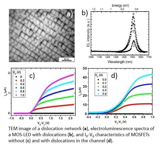
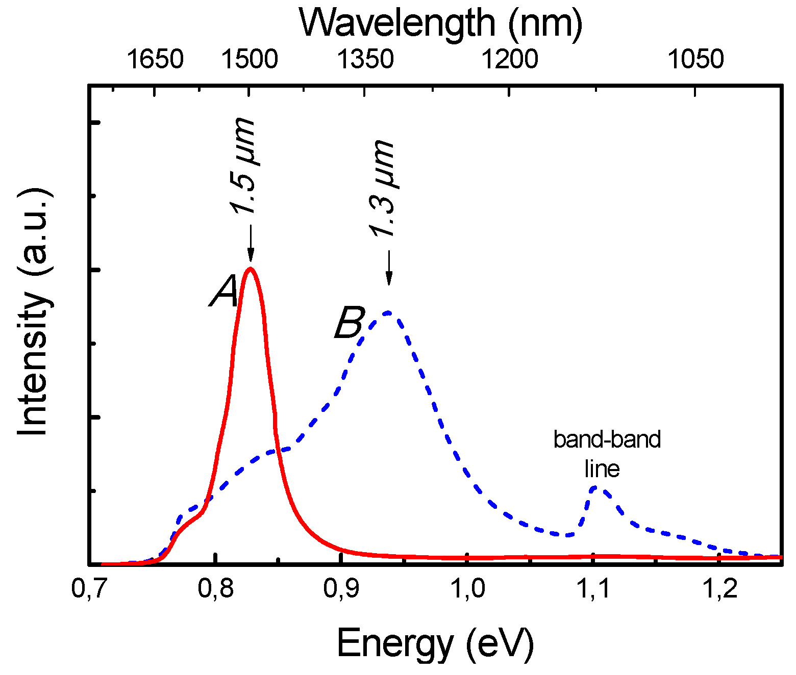
The band diagram of a tunnel MOS-LED with a dialocation network on p-type Si is schematically represented in Figure 24a, see also [108,117]. When the network is positioned near the Si/oxide interface, the radiative recombination is dominated by the D1-line at about 1.5 µm. This is clearly seen from the EL spectra shown in Figure 24b (note that band-band-luminescence around 1.1 µm appears without the dislocation network [108]). The MOS-LED on p-type Si, with a dislocation network at a depth of about 45 nm, consisted of a 134 nm thick Ti gate deposited on 1.8 nm thick tunnel silicon oxide, see TEM micrographs shown in Figure 24c. The tunneling current grows as the gate voltage increases, leading to an enhancement of the EL intensity.
Recently, we have demonstrated a dislocation-based all-silicon LED integrated in a thin SOI layer [118]. The dislocation network was inserted in an 80 nm thick SOI layer. Figure 25 shows the scheme of the LED and the measured EL spectrum. To realize an electrically pumped light emitter in SOI we prepared a two-electrode device. Two p-n junctions were fabricated locally within the p-type SOI layer. One of the junctions is used as a source (injector) and the other as a drain. Under operation the injector is forward biased and the drain is reverse biased. Therefore, the injected carriers are transported along the dislocation network. An intense EL is observed at room temperature due to radiative recombination at the network. The spectrum contains in addition to the D1-line at 1.55 μm also significant contributions of the D2- and D3-luminescence.
4. Materials and Methods
Semiconductor wafer direct bonding under hydrophobic surface conditions was applied to realize two-dimensional dislocation networks [34,119]. Varying the angles of rotational and azimuthal misfit, respectively, different dislocation distances result. The type of the dislocations forming the network is controlled by the crystal symmetry of the bonded wafers. Using {100}-oriented silicon wafers, a screw dislocation network with square-like meshes results from the rotational misfit.
Silicon-on-insulator (SOI) wafers were applied to avoid the effect of bulk material and possible defects therein. Commercially available wafers were utilized having the following specification: Czochralski-grown silicon, diameter 150 mm, p-type, resistivity ρ = 1 − 10 Ω∙cm, <100>-orientation, buried oxide thickness (BOX) 60 nm. The initial device layer thickness of 260 nm or 600 nm was reduced to 30 nm by thermal oxidation. The bonding process was performed under hydrophobic conditions in an atmospheric environment. Various twist angles in the range 0.01 < < 0.4 were realized. Figure 26 shows a schema of the process. After bonding, a subsequent annealing at 1050 °C for 4 h in nitrogen result in the formation of the two-dimensional dislocation network in the interface. Finally, one of the handle wafers was removed by a combination of mechanical grinding and chemical etching (spin etching) followed by chemical etching of the oxide layer. This results in new SOI wafers having two-dimensional dislocation networks in their 60 nm thick device layers.
SOI MOSFETs and arrays of n+pn+-diode structures were prepared on such substrates using lithographic techniques and reactive ion etching (RIE). The channel region was defined first.
The channel direction, <110>-crystal direction, which coincides with the dislocations direction in Si (Figure 27), is chosen. In order to study the effect of the dislocation density, the channel width was varied between 1 µm and 10 µm. The channel length, however, was constant (L = 1 µm). Source and drain contacts were formed by As+ implantation (5 keV, 1 × 1015 cm−2) combined with a rapid thermal annealing (RTA) step (950 °C, 60 s).
For MOSFETs, a thin gate oxide of about 6 nm was formed by thermal oxidation. The device gates were prepared by low-pressure chemical vapor deposition (LP-CVD) of polycrystalline silicon (100 nm thick) followed by As+ implantation (30 keV, 1 × 1015 cm−2) and a RTA step (950 °C, 60 s). Finally, contacts were formed by Al deposition and annealing at 420 °C for 30 min in hydrogen.
Electron beam lithography (EBL) was utilized to realize n+pn+-structures with channel widths down to 30 nm. Arrays of primary structures with W = 250 µm and L = 1 µm were prepared first by photolithography. After that EBL was used to reduce the channel width. Within an array, n+pn+-structures with 1 µm ≤ W ≤ 30 nm were realized. A high-resolution positive electron beam resist (ZEP 520A, ZEON Corp.) was used. All exposures were carried out in a JBX 6300 FS electron beam lithography system (JEOL). The real channel width of all structures was measured in a scanning electron microscope after dry etching (cryoprocess at −60 °C, SF6/O2 chemistry) and resist removing.
All device measurements were carried out at room temperature using an Agilent B1500A Semiconductor Device Analyzer in combination with a PM5 probe station (Suss). Low-temperature measurements were carried out using a cryogenic probe station (Tmin ≅ 4 K, Lake Shore Cryotronics) and a Physical Property Measurement System (PPMA, Model 6000, Tmin ≅ 2 K Quantum Design, Inc. San Diego, USA). The latter enables also measurements in magnetic fields up to 8 Tesla. A modified Heliox VL refrigator system (Oxford Instruments) was applied for measurements down to T ≅ 300 mK.
The defect structure was analyzed by applying a probe CS corrected scanning transmission electron microscope (FEI Titan 80–300).
For EBIC investigations reported here, a Cambridge Stereoscan S 360 equipped with a Matelect ISM 5 amplifier was mostly used. The measurements were performed with an Oxford cold stage.
For the luminescence investigations, a homemade system was frequently used. The luminescence spectrum was spectrally resolved by a HR 640 Jobin Yvon monochromator. A liquid nitrogen cooled North coast germanium p-i-n diode was applied for light detection.
5. Conclusions
Dislocations are one-dimensional crystal defects. Their dimensions characterize the defects as nanostructures (nanowires) exhibiting remarkable electronic and optical properties. The exceptional properties can be used effectively if defined arrays of dislocations are integrated into electronic or light emitting devices.
The integration of two-dimensional arrays of dislocations into the channel of electronic devices (MOSFETs) results in a significant increase of the drain current for n- and pMOSFETs referring to the transport of either electrons or holes along dislocations. This demonstrates the ambipolar character of dislocations in silicon. Furthermore, the drain current increases as the number of dislocations decreases. The highest drain current is measured for devices containing an individual dislocation. The resistivity of an individual dislocation was deduced to be about 1 × 10⁻⁸ Ωcm, which is about eight orders of magnitude below of the surrounding silicon. The resistivity of a dislocation is also significantly smaller than for most metals and implies a supermetallic behavior of dislocations in silicon.
A model of a dislocation as quantum wire is presented based on extensive structural analyses, electrical measurements and quantum mechanical simulations. The model presumes strong modifications of the local band structure as consequence of the extraordinary high strain level in the core of a dislocation exceeding 10 % or more. This creates a quantum wire wherein carriers are confined in one dimension.
Acknowledgments
We are thankful to E. Pippel (Halle) for TEM investigation and H. Uebensee (Erfurt), H. Kosina (Wien), and S. Birner (Munich) for fruitful discussions. M. Schmelz and H. Mühlig (Jena) are gratefully acknowledged for their help during low-temperature measurements. Parts of this work were financially supported by the German Federal Ministry of Education and Research in the framework of the SiGe-TE project (contract No. 03X3541B).
Author Contributions
Both authors contribute equally to experimental and theoretical work as well as to the manuscript preparation.
Conflicts of Interest
The authors declare no conflict of interest.
References
- Vainshtein, B.K.; Fridkin, V.M.; Indenbom, V.L. Modern Crystallography 2: Structure of Crystals; Springer: Berlin, Germany, 2000; pp. 330–399. [Google Scholar]
- Weingarten, G. Sulle superficie di discontinuitá nella teoria della elasticitá dei corpi solidi. Rend. Reale Accad dei Lincei Classe di Sci. Fis. Mater. Nat. Ser. 5 1901, 10, 57–60. [Google Scholar]
- Michell, J.H. On the direct determination of stress in an elastic solid, with application to the theory of plates. Proc. Lond. Math. Soc. 1899, 31, 100–124. [Google Scholar] [CrossRef]
- Timpe, A. Probleme der Spannungsverteilung in ebenen Systemen, einfach gelöst mit Hilfe der Airyschen Funktion. Z. Math. Phys. 1905, 52, 348–383. [Google Scholar]
- Volterra, V. Sur l′équilibre des corps élastiques multiplement connexes. Ann. Scientif. Éc. Norm. Sup. 3e Sér. 1907, 24, 401–517. [Google Scholar]
- Love, A.E.H. A Treatise on the Mathematical Theory of Elasticity; Cambridge University Press: Cambridge, UK, 1927; pp. 221–228. [Google Scholar]
- Orowan, E. Zur Kristallplastizität III. Z. Phys. 1934, 89, 634–659. [Google Scholar] [CrossRef]
- Polanyi, M. Über eine art gitterstörung, die einen Kristall plastisch machen könnte. Z. Phys. 1934, 89, 660–664. [Google Scholar] [CrossRef]
- Taylor, G.I. The mechanism of plastic deformation of crystals. Part I.—Theoretical. Proc. R. Soc. Lond. 1934, 145, 362–387. [Google Scholar] [CrossRef]
- Taylor, G.I. The mechanism of plastic deformation of crystals. Part II.—Comparison with observations. Proc. R. Soc. Lond. 1934, 145, 388–404. [Google Scholar] [CrossRef]
- Frank, F.C.I. Liquid crystals—On the theory of liquid crystals. Discuss. Faraday Soc. 1958, 25, 19–28. [Google Scholar] [CrossRef]
- Dewit, R. Theory of disclinations: II. Continuous and discrete dislclinations in anisotropic elasticity. J. Res. Nat. Bur. Stand. A Phys. Chem. 1973, 77, 49–100. [Google Scholar] [CrossRef]
- Kröner, E.; Anthony, K.-H. Dislocations and disclinations in material structures: The basic topological concepts. Annu. Rev. Mater. Sci. 1975, 5, 43–72. [Google Scholar] [CrossRef]
- Hirth, J.P. A brief history of dislocation theory. Metall. Trans. A 1985, 16, 2085–2090. [Google Scholar] [CrossRef]
- Volmer, M. Kinetik der Phasenbildung; Steinkopff: Dresden, Leipzig, Germany, 1939. [Google Scholar]
- Volmer, M.; Schultze, W. Kondensation an Kristallen. Z. Physik. Chem. 1931, 156, 1–22. [Google Scholar]
- Frank, F.C. The influence of dislocations on crystal growth. Discuss. Faraday Soc. 1949, 5, 48–54. [Google Scholar] [CrossRef]
- Frenkel, J. Zur theorie der elastizitätsgrenze und der festigkeit kristallinischer körper. Z. Phys. 1926, 37, 572–609. [Google Scholar] [CrossRef]
- Hirth, J.P.; Lothe, J. Theory of Dislocations; Wiley: New York, NY, USA, 1982. [Google Scholar]
- Hull, D.; Bacon, D.J. Introduction to Dislocations; Butterworth & Heinemann: Oxford, UK, 2010. [Google Scholar]
- Amelinckx, S. The Direct Observation of Dislocations; Academic Press: New York, NY, USA, 1965. [Google Scholar]
- Hirsch, P.B.; Horne, R.W.; Whelan, M.J. Direct observation of the arrangement and motion of dislocations in Aluminium. Philos. Mag. 1956, 1, 677–684. [Google Scholar] [CrossRef]
- Bollmann, W. Interference effects in the electron microscopy of thin crystal foils. Phys. Rev. 1956, 103, 1588–1589. [Google Scholar] [CrossRef]
- Dash, W.C. Copper precipitation on dislocations in silicon. J. Appl. Phys. 1956, 27, 1193–1195. [Google Scholar] [CrossRef]
- Ravi, K.V. Imperfections and Impurities in Semiconductor Silicon; Wiley: New York, NY, USA, 1981. [Google Scholar]
- Schröter, W.; Labusch, R. Electrical properties of dislocations in Ge and Si. Phys. Stat. Sol. 1969, 36, 539–550. [Google Scholar] [CrossRef]
- Alexander, H.; Teichler, H. Dislocations. In Materials Science and Technology, Vol. 4, Electronic Structure and Properties of Semiconductors; Schröter, W., Ed.; VCH: Weinheim, Germany, 1991; pp. 249–319. [Google Scholar]
- Drozdov, N.A.; Patrin, A.A.; Tkachev, V.D. Recombination radiation on dislocations in silicon (in russisch). Pisma Zh. Eksp. Teor. Fiz. 1976, 23, 651–653. [Google Scholar]
- Drozdov, N.A.; Patrin, A.A.; Tkachev, V.D. Recombination radiation on dislocations in silicon. Sov. Phys. JETP Lett. 1976, 23, 597–599. [Google Scholar]
- Drozdov, N.A.; Patrin, A.A.; Tkachev, V.D. On the nature of the dislocation luminescence in silicon. Phys. Stat. Sol. B 1977, 83, K137–K139. [Google Scholar] [CrossRef]
- Thibault-Desseaux, J.; Putaux, J.-L.; Bourret, A.; Kirchner, H.O.K. Dislocations stopped by the S = 9(122) grain boundary in Si. An HREM study of thermal activation. J. Phys. 1989, 50, 2525–2540. [Google Scholar] [CrossRef]
- Aubert, J.J.; Bacmann, J.J. Czochralski growth of silicon bicrystals. Rev. Phys. Appl. 1987, 22, 515–518. [Google Scholar] [CrossRef]
- Reiche, M.; Kittler, M. Structure and properties. In Crystalline Silicon—Properties and Uses; Basu, S., Ed.; Intech: Rijeka, Croatia, 2011; pp. 57–80. [Google Scholar]
- Reiche, M. Direct wafer bonding. In Handbook of Wafer Bonding; Ramm, P., Lu, J.-Q., Taklo, M.V., Eds.; Wiley-VCH: Weinheim, Germany, 2012; pp. 81–100. [Google Scholar]
- Hornstra, J. Dislocations in the diamond lattice. J. Phys. Chem. Solids 1958, 5, 129–141. [Google Scholar] [CrossRef]
- Seitz, F. The plasticity of silicon and germanium. Phys. Rev. 1952, 88, 722–724. [Google Scholar] [CrossRef]
- Amelinckx, S. Dislocations in particular structures. In Dislocations in Solids; Nabarro, F.R.N., Ed.; North-Holland: Amsterdam, The Netherlands, 1982; pp. 67–460. [Google Scholar]
- Gomez, A.; Hirsch, P.B. On the mobility of dislocations in germanium and silicon. Philos. Mag. 1977, 36, 169–179. [Google Scholar] [CrossRef]
- Ray, I.L.F.; Cockayne, D.J.H. The dissociation of dislocations in silicon. Proc. R. Soc. Lond. A 1971, 325, 543–554. [Google Scholar] [CrossRef]
- Alexander, H. Dislocations in covalent crystals. In Dislocations in Solids; Nabarro, F.R.N., Ed.; North-Holland: Amsterdam, The Netherlands, 1986; pp. 113–234. [Google Scholar]
- Duesbery, M.S.; Joós, B. Dislocation motion in silicon: The shuffle-glide controversy. Philos. Mag. Lett. 1996, 74, 253–258. [Google Scholar] [CrossRef]
- Marklund, S. Electron states associated with partial dislocations in silicon. Phys. Stat. Sol. B 1979, 92, 83–89. [Google Scholar] [CrossRef]
- Bulatov, V.V.; Cai, W. Computer Simulation of Dislocations; Oxford University Press: Oxford, UK, 2006. [Google Scholar]
- 4Smallman, R.E.; Ngan, A.H.W. Introduction to dislocations. In Modern Physical Metallurgy; Elsevier: Boston, MA, USA, 2014. [Google Scholar]
- Bourdelle, K.K.; Rayssac, O.; Lambert, A.; Fournel, F.; Hebras, X.; Allibert, F.; Figuet, C.; Boussagol, A.; Berne, C.; Tsyganenko, K.; et al. Fabrication of directly bonded Si substrates with hybrid crystal orientation for advanced bulk CMOS technology. ECS Trans. 2006, 3, 409–415. [Google Scholar]
- Toyoda, E.; Sakai, A.; Nakatsuka, O.; Isogai, H.; Senda, T.; Izunome, K.; Ogawa, M.; Zaima, S. Characterization of bonding structures of directly bonded hybrid crystal orientation substrates. Thin Solid Films 2008, 517, 323–326. [Google Scholar] [CrossRef]
- Reiche, M. Dislocation networks formed by silicon wafer direct bonding. Mater. Sci. Forum 2008, 590, 57–78. [Google Scholar] [CrossRef]
- Goodhew, P.J.; Darby, T.P.; Balluffi, R.W. On the dislocation structure of low angle (110) twist boundaries and its relationship to the O-lattice. Scr. Metall. 1976, 10, 495–499. [Google Scholar] [CrossRef]
- Reiche, M.; Kittler, M.; Uebensee, H.; Pippel, E.; Hopfe, S. Dislocations as native nanostructures-electronic properties. Adv. Nano Res. 2014, 2, 1–14. [Google Scholar] [CrossRef]
- Belov, A.Y.; Scholz, R.; Scheerschmidt, K. Dissociation of screw dislocations on (001) low-angle twist boundaries: A source of the 30° partial dislocations in silicon. Philos. Mag. Lett. 1999, 79, 531–538. [Google Scholar] [CrossRef]
- Galindo, P.L.; Krel, S.; Sanchez, A.M.; Laval, J.-Y.; Sanez, A.; Pizarro, J.; Guerrero, E.; Ben, T.; Molina, S.I. The peak pairs algorithm for strain mapping from HRTEM images. Ultramicroscopy 2007, 107, 1186–1193. [Google Scholar] [CrossRef] [PubMed]
- Alexander, H.; Gottschalk, H.; Kisielowski-Kemmerich, C. New Results on the Core of Dislocations in Silicon by EPR and TEM, in Dislocations in Solids; Suzuki, H., Ninomiya, T., Sumino, K., Takeuchi, S., Eds.; University of Tokyo Press: Tokyo, Japan, 1985; pp. 337–342. [Google Scholar]
- Blumenau, A.T. The Modelling of Dislocations in Semiconductor Crystals. Ph.D. Thesis, University of Paderborn, Paderborn, Germany, 2002. [Google Scholar]
- Zhao, C.W.; Xing, Y.M. Nanoscale strain analysis of an edge dislocation. Proc. SPIE 2008. [Google Scholar] [CrossRef]
- Kittler, M.; Yu, X.; Mchedlidze, T.; Arguirov, T.; Vyvenko, O.F.; Seifert, W.; Reiche, M.; Wilhelm, T.; Seibt, M.; Voß, O.; et al. Regular dislocation networks in silicon as a tool for nanostructure devices used in optics, biology, and electronics. Small 2007, 3, 964–973. [Google Scholar] [CrossRef] [PubMed]
- Reiche, M.; Kittler, M.; Pippel, E.; Erfurth, W.; Haehnel, A.; Uebensee, H. Strain and carrier transport along dislocations. Phys. Stat. Sol. C 2015, 12, 1071–1076. [Google Scholar] [CrossRef]
- Ishikawa, Y.; Yamamoto, C.; Tabe, M. Single-electron tunneling in a silicon-on-insulator layer embedding an artificial dislocation network. Appl. Phys. Lett. 2006, 88, 0731121–0731123. [Google Scholar] [CrossRef]
- Reiche, M.; Kittler, M.; Scholz, R.; Hähnel, A.; Arguirov, T. Structure and properties of dislocations in interfaces of bonded silicon wafers. J. Phys. Conf. Ser. 2011. [Google Scholar] [CrossRef]
- Reiche, M.; Kittler, M.; Erfurth, W.; Pippel, E.; Sklarek, K. On the electronic properties of a single dislocation. J. Appl. Phys. 2014. [Google Scholar] [CrossRef]
- Liu, Z.-H.; Hu, C.; Huang, J.-H.; Chan, T.-Y.; Jeng, M.-C.; Ko, P.K.; Cheng, Y.C. Threshold voltage model for deep-submicrometer MOSFETs. IEEE Trans. Electron Dev. 1993, 40, 86–94. [Google Scholar] [CrossRef]
- Rauly, E.; Potavin, O.; Balestra, F.; Raynaud, C. On the subthreshold swing and short channel effects in singl and double gate deep submicron SOI-MOSFETs. Solid State Electron. 1999, 43, 2033–2037. [Google Scholar] [CrossRef]
- Reiche, M.; Kittler, M.; Krause, M.; Uebensee, H. Electrons on dislocations. Phys. Stat. Sol. C 2013, 10, 40–43. [Google Scholar] [CrossRef]
- Kittler, M.; Kveder, V. Dislocations in silicon and D-band luminescence for infrared light emitters. Mater. Sci. Forum 2008, 590, 29–56. [Google Scholar]
- Labusch, R.; Schröter, W. Electrical properties of dislocations in semiconductors. In Dislocations in Solids; Nabarro, F.R.N., Ed.; North-Holland: Amsterdam, The Netherlands, 1980; pp. 127–191. [Google Scholar]
- Reiche, M.; Kittler, M.; Uebensee, H.; Pippel, E. A novel SOI-based MOSFET with ultra-low subthreshold swing for cryogenic applications. In Proceedings of the 2013 Symposium on Microelectronics Technology and Devices (SBMicro), Curitiba, Brasil, 2–6 September 2013; pp. 1–3.
- Klaassen, D.B.M. A unified mobility model for device simulation—I. Model equations and concentration dependence. Solid State Electron. 1992, 35, 953–959. [Google Scholar] [CrossRef]
- Reiche, M.; Kittler, M.; Schmelz, M.; Stolz, R.; Pippel, E.; Uebensee, H.; Kermann, M.; Ortlepp, T. Single-electron transitions in one-dimensional native nanostructures. J. Phys. Conf. Ser. 2014, 568, 052024. [Google Scholar] [CrossRef]
- Ando, T.; Fowler, A.B.; Stern, F. Electronic properties of two-dimensional systems. Rev. Mod. Phys. 1982, 54, 437–672. [Google Scholar] [CrossRef]
- Ihn, T. Semiconductor Nanostructures: Quantum States and Electronic Transport; Oxford University Press: New York, NY, USA, 2010. [Google Scholar]
- Kouwenhoven, L.P.; Marcus, C.M.; McEuen, P.L.; Tarucha, S.; Westervelt, R.M.; Wingreen, N.S. Electron transport in quantum dots. In Mesoscopic Electron Transport; Sohn, L.L., Kouwenhoven, L.P., Schön, G., Eds.; Kluwer: Dordrecht, The Netherlands, 1997. [Google Scholar]
- Tilke, A.T.; Simmel, F.C.; Blick, R.H.; Lorenz, H.; Kotthaus, J.P. Coulomb blockade in silicon nanostructures. Progr. Quant. Electron. 2001, 25, 97–138. [Google Scholar] [CrossRef]
- Zhong, Z.; Fang, Y.; Lu, W.; Lieber, C.M. Coherent single charge transport in molecular-scale silicon nanowires. Nano Lett. 2005, 5, 1143–1146. [Google Scholar] [CrossRef] [PubMed]
- Gallagher, C.J. Plastic deformation of germanium and silicon. Phys. Rev. 1952, 88, 721–722. [Google Scholar] [CrossRef]
- Pearson, G.L.; Read, W.T.; Morin, F.J. Dislocations in plastically deformed germanium. Phys. Rev. 1954, 93, 666–667. [Google Scholar] [CrossRef]
- Read, W.T. Theory of dislocations in germanium. Philos. Mag. 1954, 45, 775–796. [Google Scholar] [CrossRef]
- Read, W.T. Statistics of the occupation of dislocation acceptor centres. Philos. Mag. 1954, 45, 1119–1128. [Google Scholar] [CrossRef]
- Schröter, W. Trägerbeweglichkeit in verformtem Germanium. Phys. Stat. Sol. 1969, 31, 177–186. [Google Scholar] [CrossRef]
- Weber, H.; Schröter, W.; Haasen, P. Elektronenzustände an Versetzungen in Silizium. Helv. Phys. Acta 1968, 41, 1255–1258. [Google Scholar]
- Veth, H.; Lannoo, M. The electronic properties of charged dislocations in semiconductors. Philos. Mag. B 1984, 50, 93–102. [Google Scholar] [CrossRef]
- Reiche, M.; Kittler, M.; Uebensee, H.; Pippel, E.; Haehnel, A.; Birner, S. Electronic properties of dislocations. Appl. Phys. A 2016, 122, 389. [Google Scholar] [CrossRef]
- Fischetti, M.V.; Ren, Z.; Solomon, P.M.; Yang, M.; Rim, K. Six-band k.p calculation of the hole mobility in silicon inversion layers: Dependence on surface orientation, strain, and silicon thickness. J. Appl. Phys. 2003, 94, 1079–1095. [Google Scholar] [CrossRef]
- Sverdlov, V. Strain-Induced Effects in Advanced MOSFETs. Computational Microelectronics; Selberherr, S., Ed.; Springer: Wien, Austria, 2011. [Google Scholar]
- Maegawa, T.; Yamauchi, T.; Hara, T.; Tsuchiya, H.; Ogawa, M. Strain effects on electronic bandstructures in nanoscaled silicon: From bulk to nanowire. IEEE Trans. Electron. Dev. 2009, 56, 553–559. [Google Scholar] [CrossRef]
- Ungersboeck, E.; Dhar, S.; Karlowatz, G.; Sverdlov, V.; Kosina, H.; Selberherr, S. The effect of general strain on the band structure and electron mobility of silicon. IEEE Trans. Electron. Dev. 2007, 54, 2183–2190. [Google Scholar] [CrossRef]
- Shiri, D.; Kong, Y.; Buin, A.; Anantram, M.P. Strain induced change of bandgap and effective mass in silicon nanowires. Appl. Phys. Lett. 2008. [Google Scholar] [CrossRef]
- Karazhanov, S.Z.; Davletova, A.; Ulyashin, A. Strain-induced modulation of band structure of silicon. J. Appl. Phys. 2008, 104, 024501. [Google Scholar] [CrossRef]
- Birner, S.; Zibold, T.; Andlauer, T.; Kubis, T.; Sabathil, M.; Trellakis, A.; Vogl, P. Nextnano: General purpose 3-D simulations. IEEE Trans. Electron Dev. 2007, 54, 2137–2142. [Google Scholar] [CrossRef]
- Jancu, J.-M.; Scholz, R.; Beltram, F.; Bassani, F. Empirical spds* tight-binding calculation for cubic semiconductors: General method and material parameters. Phys. Rev. B 1998, 57, 6493–6507. [Google Scholar] [CrossRef]
- Cohen, M.L.; Chelikowsky, J. Electronic Structure and Optical Properties of Semiconductors; Springer: Berlin, Germany, 1989. [Google Scholar]
- Ungersboeck, E. Numerische Berechnung der Bandstruktur von Halbleitern. Master’s Thesis, Vienna University of Technology, Wien, Austria, 2002. [Google Scholar]
- Ungersboeck, E.; Dhar, S.; Karlowatz, G.; Kosina, H.; Selberherr, S. Physical modeling of electron mobility enhancement for arbitrarily strained silicon. J. Comput. Electron. 2007, 6, 55–58. [Google Scholar] [CrossRef]
- Kittler, M.; Reiche, M.; Krause, M. Charge carrier transport along grain boundaries in silicon. Solid State 2013. [Google Scholar] [CrossRef]
- Reiche, M.; Kittler, M.; Krause, M.; Uebensee, H. Carrier transport on dislocations in silicon. AIP Conf. Proc. 2014, 1583, 33–36. [Google Scholar]
- Schröter, W.; Cerva, H. Interaction of point defects with dislocations in silicon and germanium: Electrical and optical effects. Solid State Phenom. 2002, 85–86, 67–144. [Google Scholar] [CrossRef]
- Bondarenko, A.; Vyvenko, O.F.; Isakov, I. Electron levels and luminescence of dislocation networks formed by the hydrophilic bonding of silicon wafers. Semiconductors 2013, 47, 223–227. [Google Scholar] [CrossRef]
- Knobloch, K.; Seifert, W.; Kittler, M. Application of scanning deep level transient spectroscopy for characterisation of multicrystalline silicon. Mater. Sci. Eng. 1996, 42, 254–259. [Google Scholar] [CrossRef]
- Donolato, C. Quantitative characterization of semiconductor defects by electron beam induced currents. In Point and Extended Defects in Semiconductors; Benedek, G., Cavallini, A., Schröter, W., Eds.; Plenum Press: New York, NY, USA, 1989; pp. 225–242. [Google Scholar]
- Kittler, M.; Ulhaq-Bouillet, C.; Higgs, V. Influence of copper contamination on recombination activity of misfit dislocations in SiGe/Si epilayers: Temperature dependence of activity as a marker characterizing the contamination level. J. Appl. Phys. 1995, 78, 4573–4583. [Google Scholar] [CrossRef]
- Kittler, M.; Seifert, W. Two classes of defect recombination behavior in silicon as studied by SEM-EBIC. Scan. Microsc. 1993, 15, 316–321. [Google Scholar]
- Kittler, M.; Seifert, W.; Higgs, V. Recombination activity of misfit dislocations in silicon. Phys. Stat. Sol. A 1993, 137, 327–335. [Google Scholar] [CrossRef]
- Knobloch, K.; Kittler, M.; Seifert, W.; Simon, J.J.; Périchaud, I. Impact of phosphorous diffusion on the contamination level of dislocations in deformed float zone silicon as studied by beam injection techniques. Solid State Phenom. 1998, 63–64, 105–114. [Google Scholar] [CrossRef]
- Kusanagi, S.; Sekiguchi, T.; Shen, B.; Sumino, K. Electrical activity of extended defects and gettering of metallic impurities in silicon. Mater. Sci. Technol. 1995, 11, 685–690. [Google Scholar]
- Shen, B.; Sekiguchi, T.; Zhang, R.; Shi, Y.; Shi, H.; Yang, K.; Zheng, Y.; Sumino, K. Precipitation of Cu and Fe in dislocated floating-zone-grown silicon. Jpn. J. Appl. Phys. 1996, 35, 3301–3305. [Google Scholar] [CrossRef]
- Kveder, V.; Kittler, M.; Schröter, W. Recombination activity of contaminated dislocations in silicon: A model describing electron-beam-induced current contrast behavior. Phys. Rev. B 2001. [Google Scholar] [CrossRef]
- Wilshaw, P.R.; Booker, G.R. New results and an interpretation for SEM EBIC contrast arising from individual dislocations in silicon. Inst. Phys. Conf. Ser. 1985, 76, 329–336. [Google Scholar]
- Knobloch, K.; Kittler, M.; Seifert, W. Influence of contamination on the dislocation-related deep level C1 line observed in deep-level-transient spectroscopy of n-type silicon: A comparison with the technique of electron-beam-induced current. J. Appl. Phys. 2003, 93, 1069–1074. [Google Scholar] [CrossRef]
- Kittler, M.; Seifert, W. Estimation of the upper limit of the minority-carrier diffusion length in multicrystalline silicon: Limitation of the action of gettering and passivation on dislocations. Solid State Phenom. 2004, 95–96, 197–204. [Google Scholar] [CrossRef]
- Kittler, M.; Mchedlidze, T.; Arguirov, T.; Seifert, W.; Reiche, M.; Wilhelm, T. Silicon based IR light emitters. Phys. Stat. Sol. C 2009, 6, 707–715. [Google Scholar] [CrossRef]
- Mchedlidze, T.; Kittler, M. Investigation of defect states in heavily dislocated thin silicon films. J. Appl. Phys. 2012, 111, 053706. [Google Scholar] [CrossRef]
- Arguirov, T. Electro-Optical Properties of Dislocations in Silicon and Their Posssible Application for Light Emitters. Ph.D. Thesis, Brandenburg Technology University, Cottbus, Germany, 2007. [Google Scholar]
- Mchedlidze, T.; Arguirov, T.; Kittler, M.; Hoang, T.; Holleman, J.; Schmitz, J. Influence of electric field on spectral positions of dislocation-related luminescence peaks in silicon: Stark effect. Appl. Phys. Lett. 2007, 91, 201113. [Google Scholar] [CrossRef]
- Sauer, R.; Weber, J.; Stolz, J.; Weber, E.R.; Küsters, K.-H.; Alexander, H. Dislocation-related photoluminescence in silicon. Appl. Phys. A 1985, 36, 1–13. [Google Scholar] [CrossRef]
- Kittler, M.; Arguirov, T.; Reiche, M.; Krause, M.; Mankovics, D. About dislocation and oxygen related luminescence of Si around 0.8 eV. Phys. Stat. Sol. C 2015, 12, 1077–1080. [Google Scholar] [CrossRef]
- Higgs, V.; Goulding, M.; Brinklow, A.; Kighthley, P. Characterization of epitaxial and oxygen-induced stacking faults in silicon: The influence of transition-metal contamination. Appl. Phys. Lett. 1992, 60, 1369–1371. [Google Scholar] [CrossRef]
- Mchedlidze, T.; Wilhelm, T.; Arguirov, T.; Trushin, M.; Reiche, M.; Kittler, M. Correlation of electrical and luminescence properties of dislocation networkswith its microscopic structure. Phys. Stat. Sol. C 2009, 6, 1817–1822. [Google Scholar] [CrossRef]
- Yu, X.; Seifert, W.; Vyvenko, O.F.; Kittler, M.; Wilhelm, T.; Reiche, M. A pure 1.5 µm electroluminescence from metal-oxide-silicon tunneling diode using dislocation network. Appl. Phys. Lett. 2008, 93, 041108. [Google Scholar] [CrossRef]
- Kittler, M.; Reiche, M.; Yu, X.; Arguirov, T.; Seifert, W.; Vyvenko, O.F. 1.5 µm emission from a silicon MOS-LED based on a dislocation network. IEDM Technol. Dig. 2006, 845–848. [Google Scholar] [CrossRef]
- Kittler, M.; Reiche, M.; Arguirov, T. 1.55 µm light emitter based on dislocation D1-emission in silicon. In Proceedings of the 2013 Symposium on Microelectronics Technology and Devices (SBMicro), Curitiba, Brasil, 2–6 September 2013.
- Tong, Q.-Y.; Gösele, U. Semiconductor Wafer Bonding: Science and Technology; Wiley: New York, NY, USA, 1999. [Google Scholar]
Figure 1.
Plots of the stress components σyz (a) and σxz (b) of a screw dislocation. The stress outside the dislocation core reaches values up to about 200 MPa. The scale shows the stress in GPa.
Figure 1.
Plots of the stress components σyz (a) and σxz (b) of a screw dislocation. The stress outside the dislocation core reaches values up to about 200 MPa. The scale shows the stress in GPa.

Figure 2.
Plots of the stress components σxx (a), σyy (b), and σxy (c) of an edge dislocation. The scale shows the stress in GPa.
Figure 2.
Plots of the stress components σxx (a), σyy (b), and σxy (c) of an edge dislocation. The scale shows the stress in GPa.
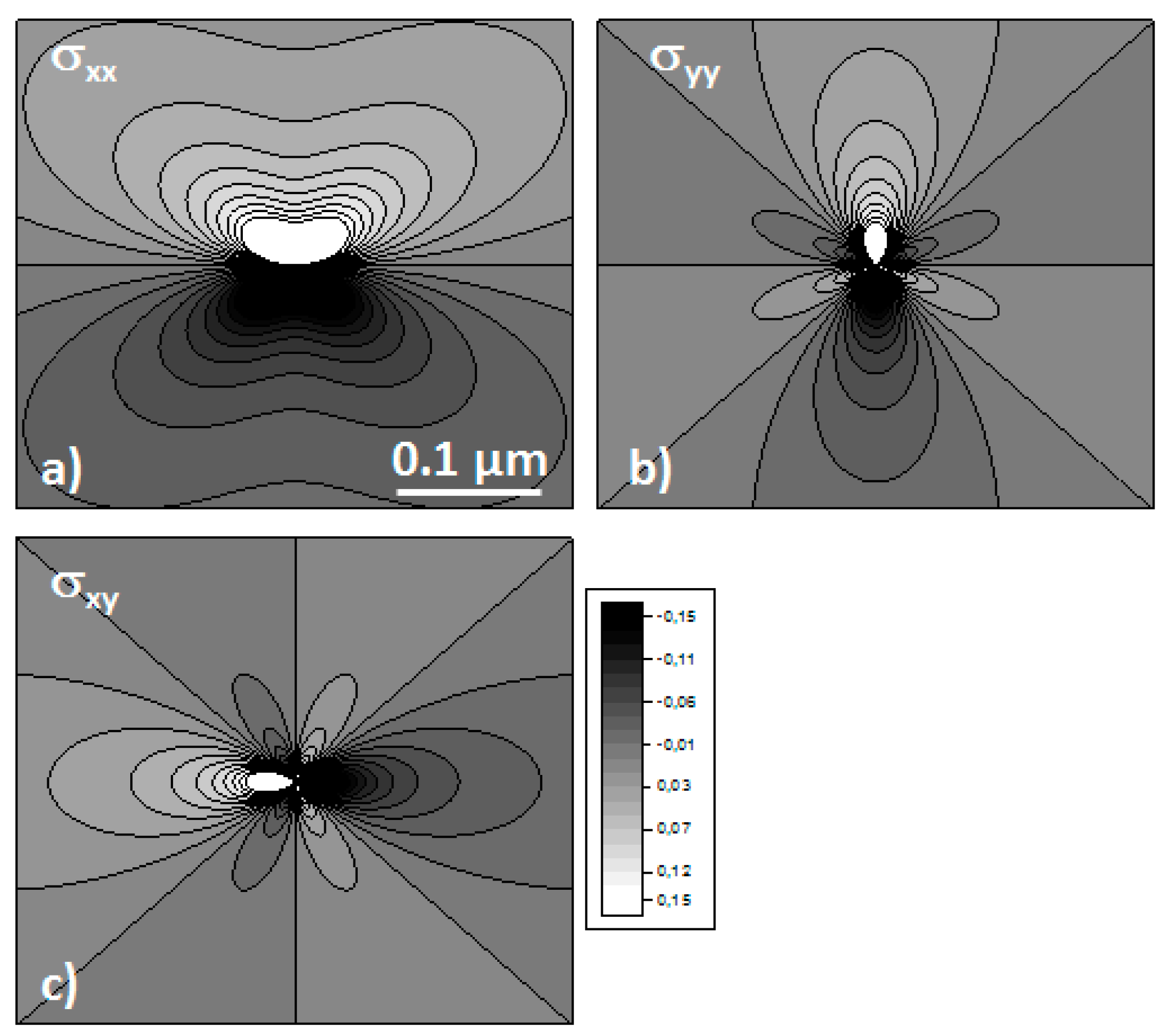
Figure 3.
Transmission electron microscopic images of dislocation networks formed by wafer bonding of wafers with different surface orientation indicated in the figures.
Figure 3.
Transmission electron microscopic images of dislocation networks formed by wafer bonding of wafers with different surface orientation indicated in the figures.

Figure 4.
Part of the dislocation network of a (110)/(110) bond wafer pair shown in Figure 3 and schematic representation of the dislocation structure. The numbers specify the corresponding Burgers vectors listed on the right side.
Figure 4.
Part of the dislocation network of a (110)/(110) bond wafer pair shown in Figure 3 and schematic representation of the dislocation structure. The numbers specify the corresponding Burgers vectors listed on the right side.
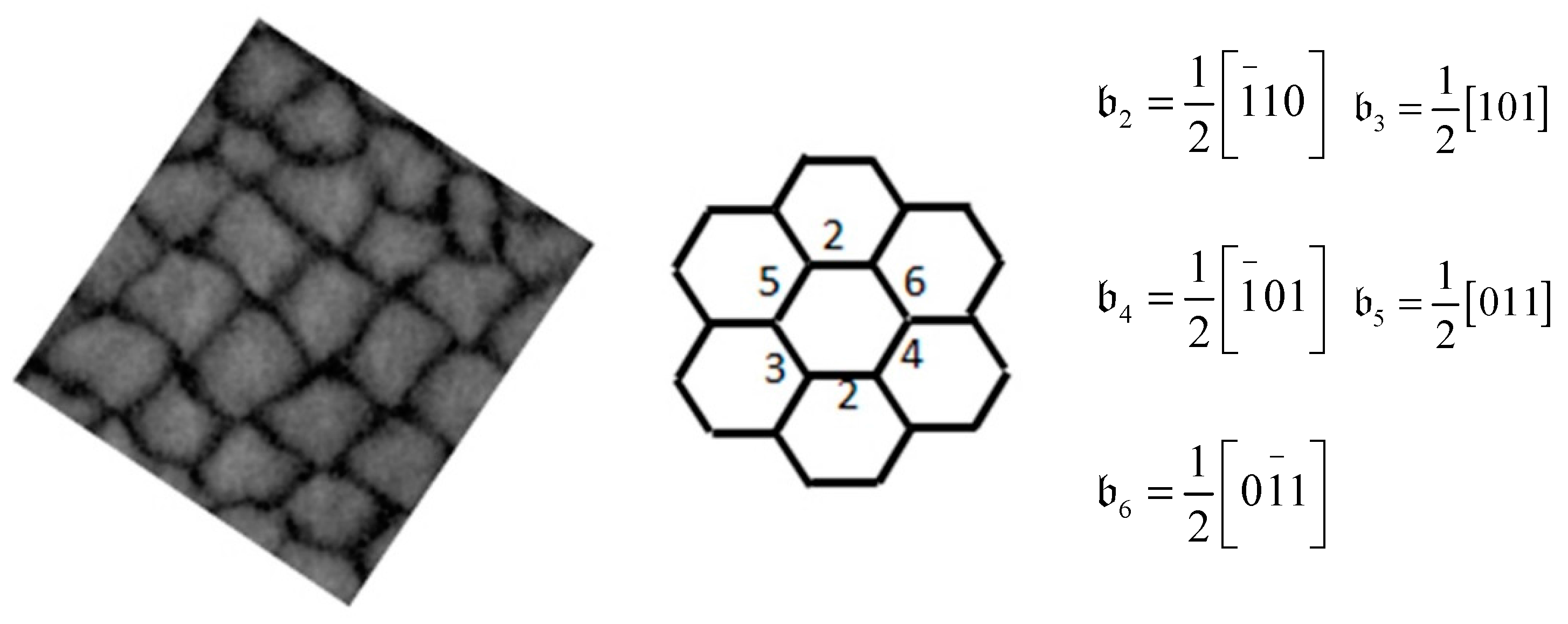
Figure 5.
High resolution electron microscopic images of individual dislocations in the interface of a (100)/(100) bonded wafer pair. The cross-sectional samples were prepared parallel to {110}.
Figure 5.
High resolution electron microscopic images of individual dislocations in the interface of a (100)/(100) bonded wafer pair. The cross-sectional samples were prepared parallel to {110}.
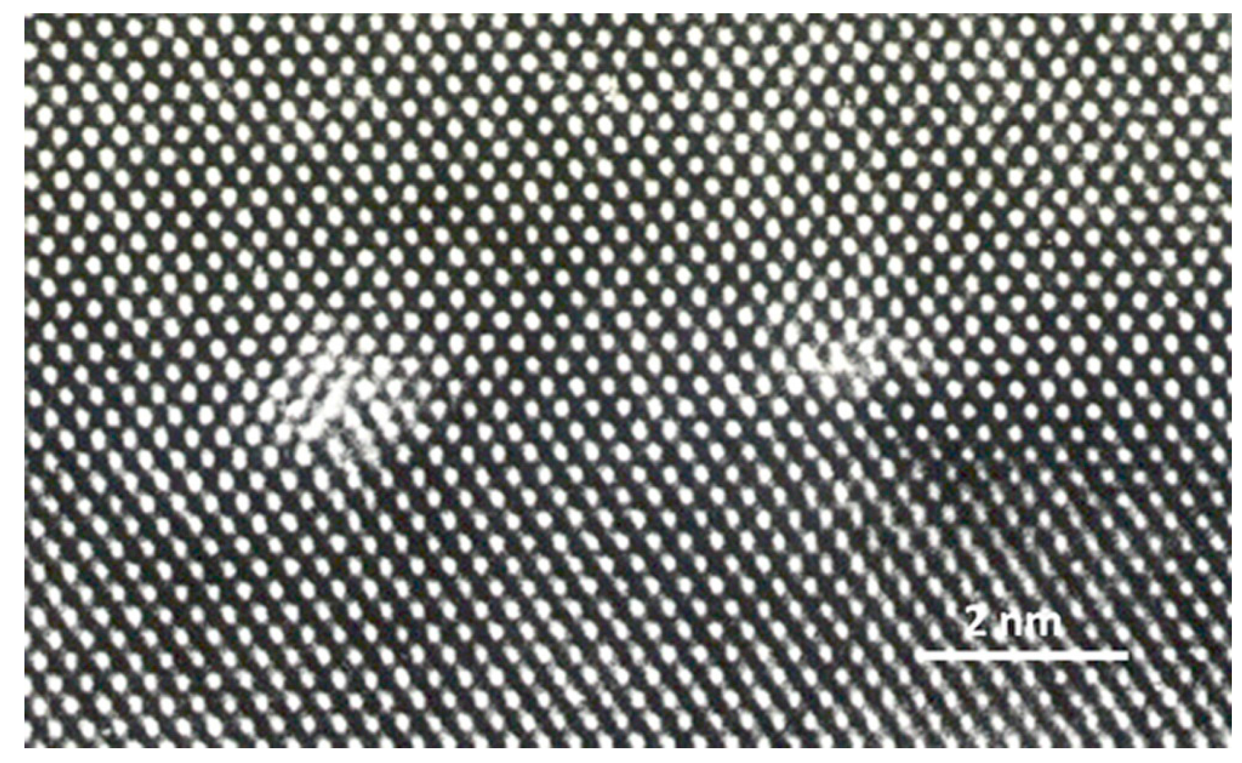
Figure 6.
High-angle annular dark field electron microscope image of a dissociated screw dislocation (a); A {110} cross section sample was used for imaging. The resulting in-plane strain (εxy) in the {110} plane is tensile (εxy ≅ 10%) and concentrated on the partial dislocations (b); The scale characterizes the strain in percent. Positive values denote tensile strain, while negative values are related to compressive strain; (c) Model of the atomic structure of the dissociated screw dislocation shown in (a). A red color characterizes atoms of the undisturbed silicon lattice, while dark blue color denotes atoms of the 30° partial dislocations, and light blue color indicates atoms in the stacking fault.
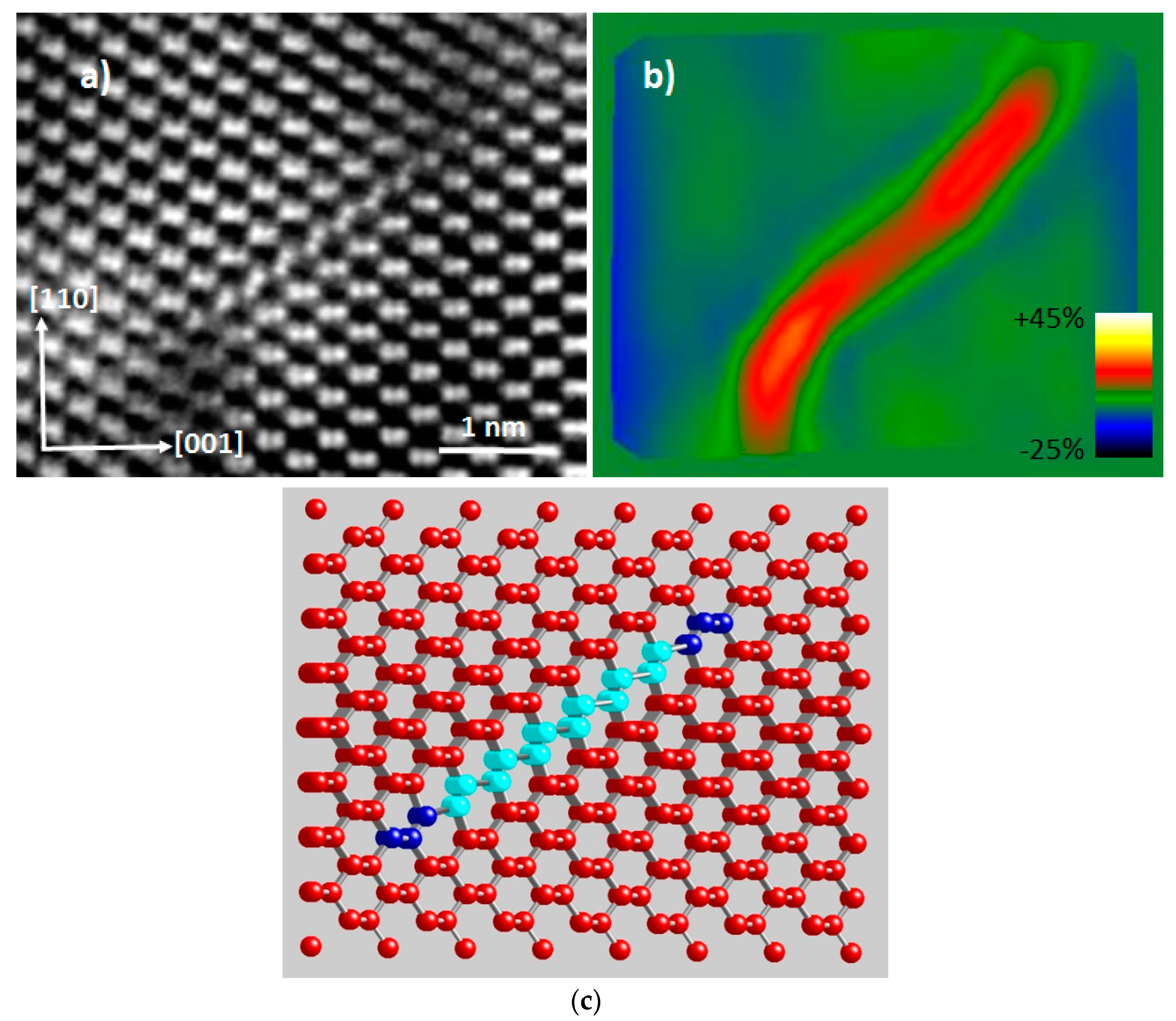
Figure 7.
Transmission electron microscopic images of cross-sectional samples prepared from a bonded SOI wafer with a dislocation network in the device layer (a) and from the channel region of a nMOSFET (b). The figure shows a part of the gate complex of a MOSFET. The polycrystalline gate electrode on top of a thin gate oxide. The gate, about 50 nm thick, is characterized by a dislocation network close to the center.


Figure 8.
Output and transfer characteristics of nMOSFETS without dislocations (a,b) and with a dislocation network (c,d). The device layer thickness was 80 nm. The channel length and width, respectively, for both devices are 1 μm. Caused by the different threshold voltages (VT) of both devices, the gate voltage (VG) is represented for clarity as VG–VT.
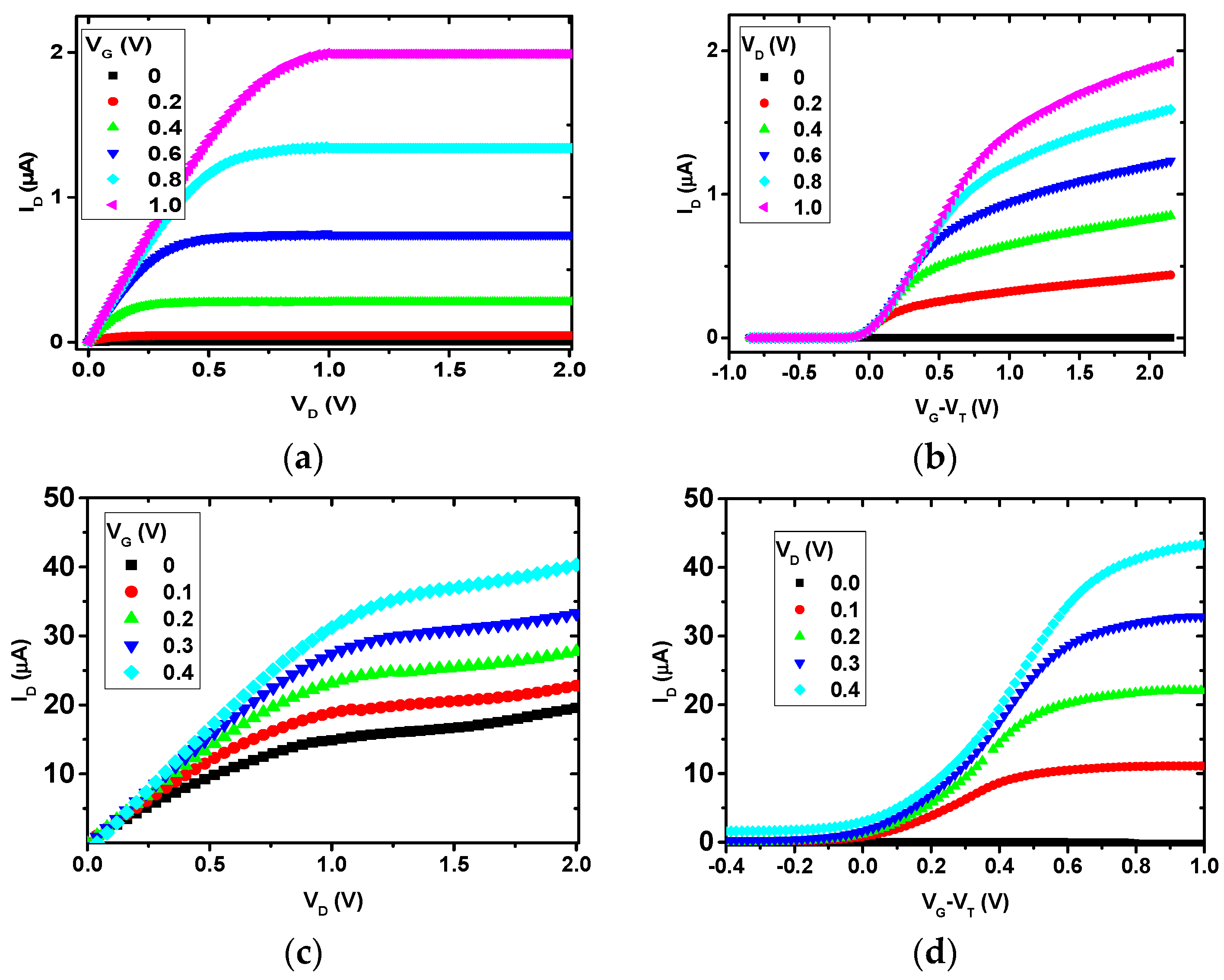
Figure 9.
Measured (full symbols) and calculated temperature-dependent transconductance gm (open symbols) of devices without (reference, squares) and with dislocations (type A, triangles) in the channel of a nMOSFET (a). Computed electron density n vs. reciprocal temperature for devices without and with dislocations (b).
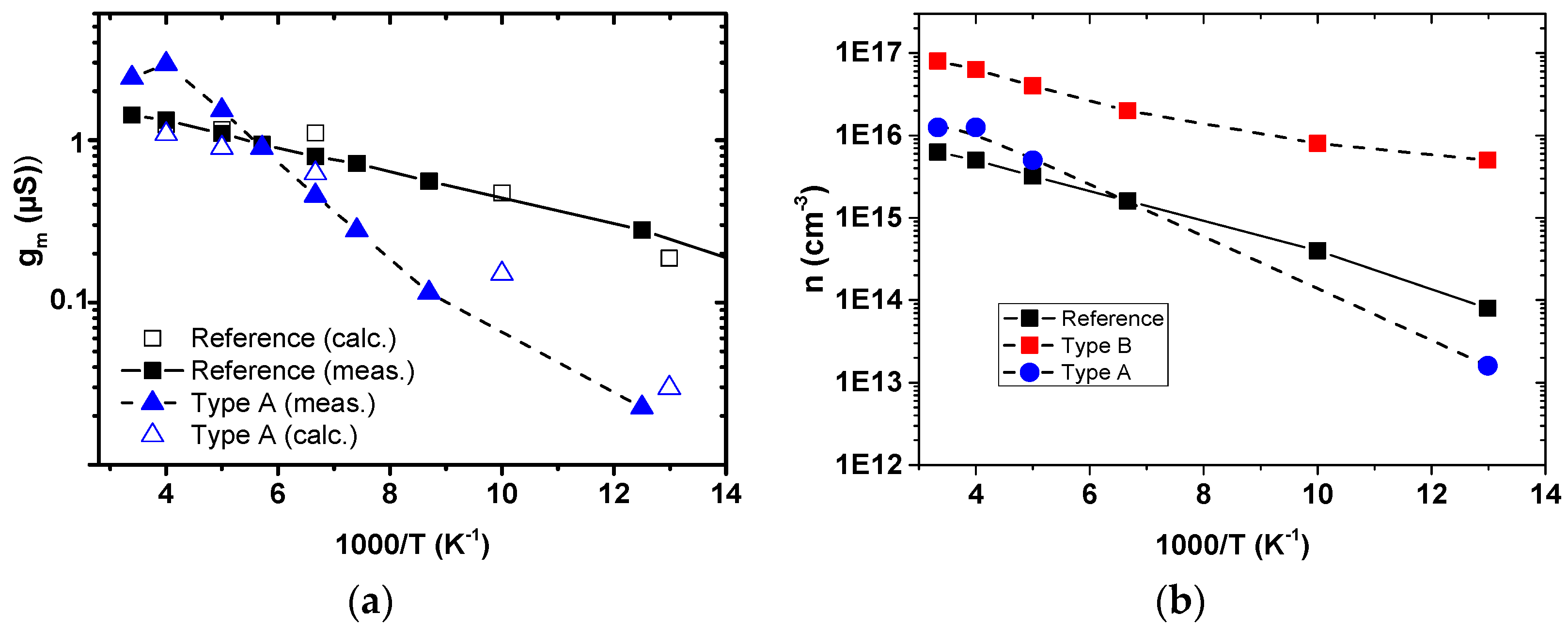
Figure 10.
Transversal and longitudinal source drain resistivity (ΔR/R) as a function of the inverse magnetic field B. Measurement on a nMOSFET with a dislocation network (VD = 3 V) at 3.1 K.
Figure 10.
Transversal and longitudinal source drain resistivity (ΔR/R) as a function of the inverse magnetic field B. Measurement on a nMOSFET with a dislocation network (VD = 3 V) at 3.1 K.

Figure 11.
Experimentally measured and calculated SdH oscillations. Measurements of dσ/dB were carried out at T = 380 mK. Calculations were performed by applying Equation (13).
Figure 11.
Experimentally measured and calculated SdH oscillations. Measurements of dσ/dB were carried out at T = 380 mK. Calculations were performed by applying Equation (13).

Figure 12.
Extraction of the electron density in the 2DEG (a) and lifetime of quantum states (b) from measurements of SdH oscillations. The procedure is described in the text.
Figure 12.
Extraction of the electron density in the 2DEG (a) and lifetime of quantum states (b) from measurements of SdH oscillations. The procedure is described in the text.

Figure 13.
Coulomb blockade oscillations as a function of gate-source voltage (VG) measured at VD = 400 mV (a). The spacing between individual blockades is 45 meV. Peak splitting in the presence of a magnetic field (b). The figure shows Coulomb blockades without a magnetic field (blue line) and in the presence of a magnetic field with B = 2T (red line). Note that the splitting is larger than the Zeeman splitting. Coulomb blockades observed on a dislocation network consisting of mixed dislocations (c,d). Blockades appear at negative (c) and positive bias (d), indicating single-electron and single-hole transitions on the same dislocations. All measurements at temperatures T = 380 mK.

Figure 14.
Band structure of silicon calculated by tight binding method (a) and part of the band structure in <100>-directions (b) calculated using the tight binding (lines) and empirical pseudopotential methods (symbols), respectively.
Figure 14.
Band structure of silicon calculated by tight binding method (a) and part of the band structure in <100>-directions (b) calculated using the tight binding (lines) and empirical pseudopotential methods (symbols), respectively.

Figure 15.
Band structure of silicon with increasing tensile strain of 4% (ε = +0.04), 8% (ε = +0.08), and 10% (ε = +0.1). Only the two lowest conduction bands are shown. The blue, magenta, and red lines indicate the heavy hole, light hole, and split-off bands, respectively. The dotted lines indicate the band gap for unstrained silicon.

Figure 16.
Direct and indirect band gaps (a) and Schema of the band diagram of a Si channel with a dislocation in the center (b). The shift of the conduction band of the strained dislocation core results in a one-dimensional defect band in the gap of the surrounding channel. For calculation, uniaxial strain (ε[110] = +0.1, tensile) is assumed. The valence band maximum was set to zero. Dotted lines designate the band gap in the unstrained silicon (Eg = 1.115 eV).

Figure 17.
Band alignment for a dislocation in a MOSFET channel. A uniaxial tensile strain of ε = +0.1 and a radius of the dislocation of R = 2.5 nm were assumed. An overview about the energies of the conduction band minima at Γ, L, and Δ as well as valence band maxima of heavy holes (hh) and light holes (lh) extracted from band structure calculations (a). Detail of the conduction band forming the quantum wire (b). The dashed lines characterize the first energy levels calculated for the quantum wire.

Figure 18.
Two-dimensional quantum mechanical device simulation. Schema of the nMOSFET with channel width and height of 20 nm (a). The channel (green) is unstrained silicon with a dislocation (2nm × 2 nm) in the center (white). Gate oxide and BOX are drawn in black, while the gate electrode is shown in yellow. The first wave function is localized in the dislocation if uniaxial tensile strain (ε = +0.1) is applied (b). Electron densities for devices with a dislocation in the center (c) and an unstrained Si channel (d). Red means the highest and black the lowest electron densities. The gate voltage is VG = 0.5 V.

Figure 19.
(a) Temperature dependencies of EBIC contrast Cdisl(T) of dislocations in Si. Points are experimental data [98], solid curves are calculated using the model [104]. (b) Charge carrier recombination at dislocations. For clean dislocations the recombination rate is determined by direct recombination of electrons and holes captured by the 1D dislocation bands EDe, EDh, see channel (1). In presence of defects with deep energy level EDD, the carriers captured to 1D-bands can recombine by the paths (3) via this deep level [104].
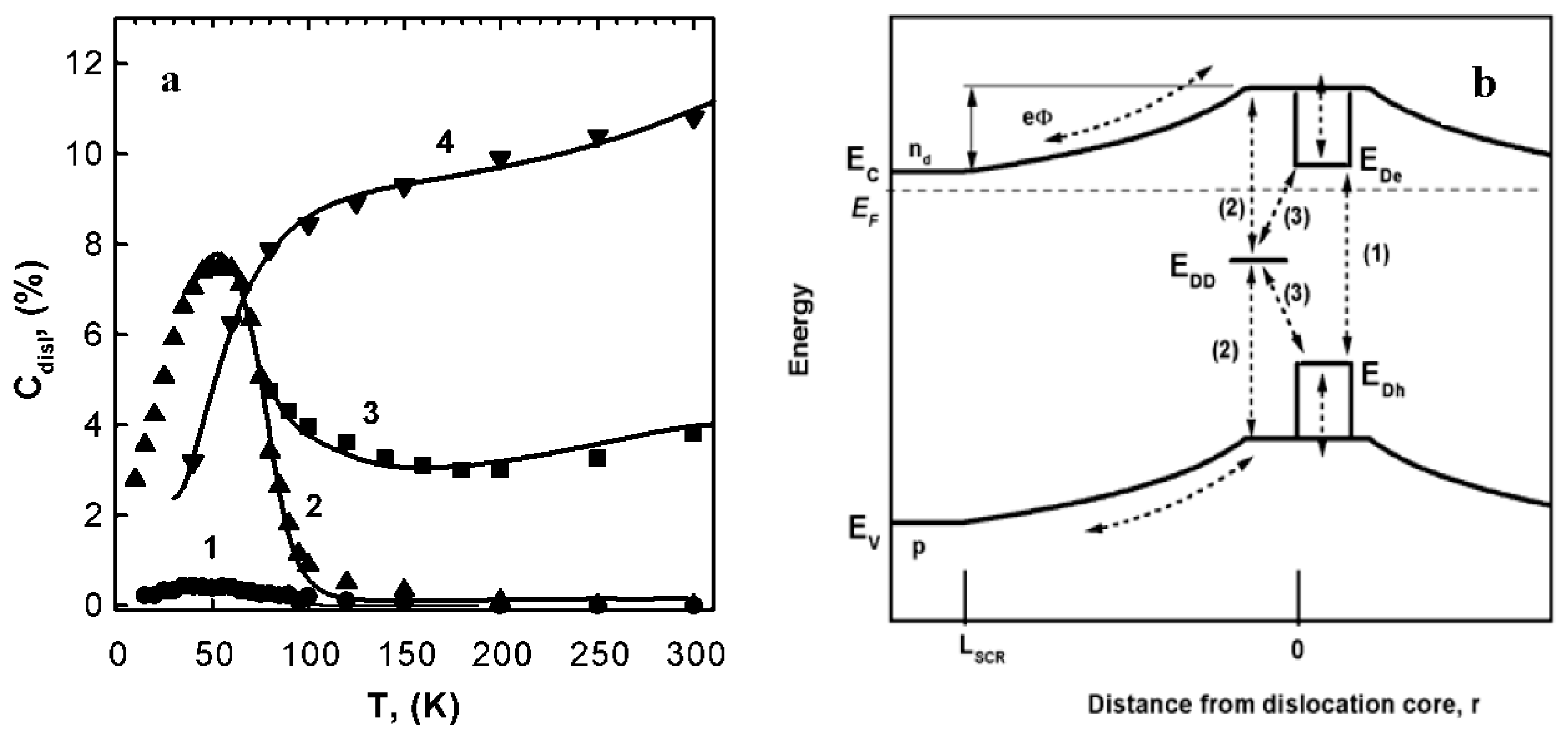
Figure 20.
Luminescence spectrum, taken at 80 K, obtained from a plastically deformed silicon sample showing the dislocation lines (D1–D4) and band-to-band (BB) radiation.
Figure 20.
Luminescence spectrum, taken at 80 K, obtained from a plastically deformed silicon sample showing the dislocation lines (D1–D4) and band-to-band (BB) radiation.
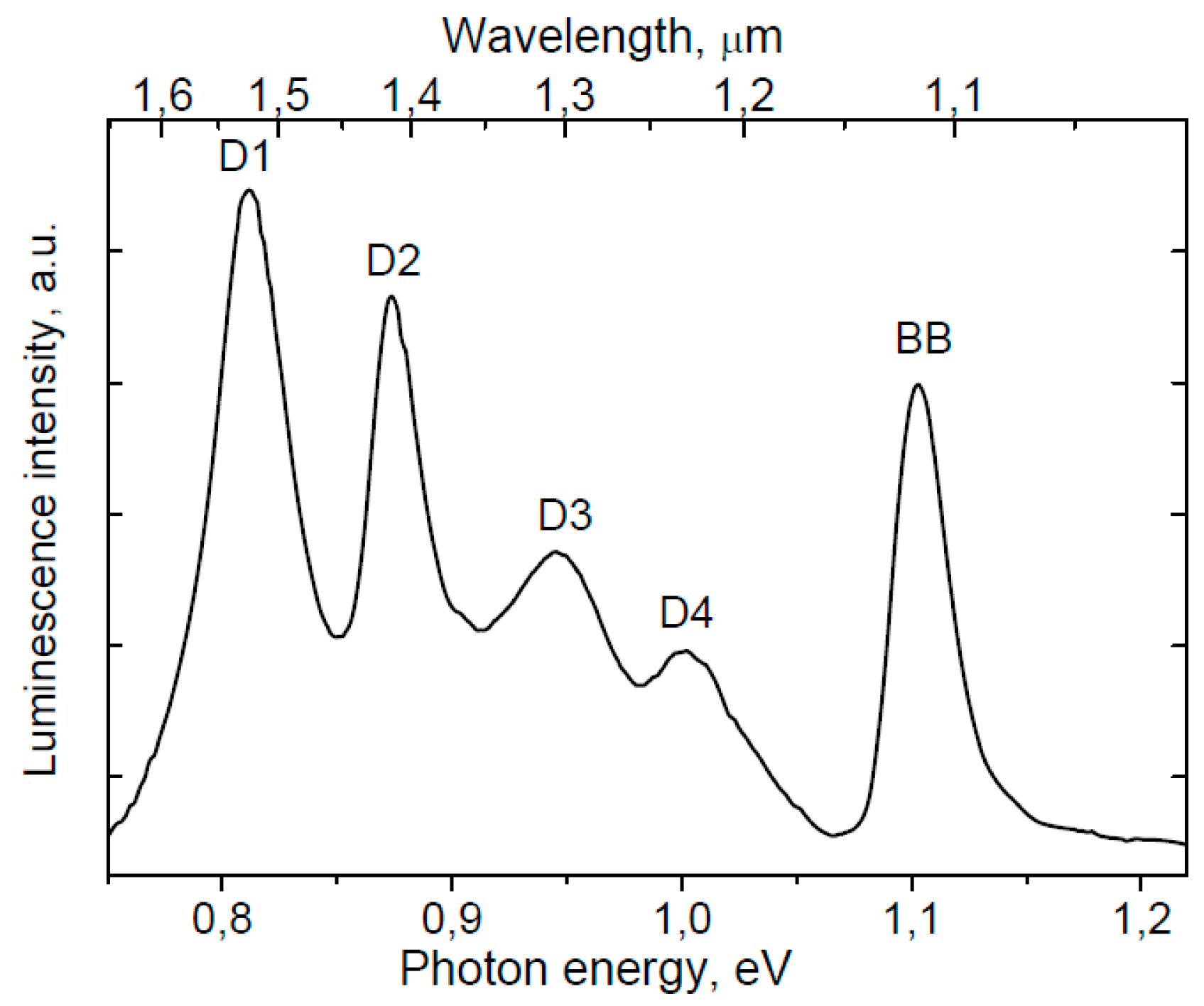
Figure 21.
Spatial distribution of D2/D1 and D4/D3 peak area ratios along a profile measured in multi-crystalline Si at T = 80 K. The ratio D2/D1 varies strongly, whereas D4/D3 remains nearly constant [110].
Figure 21.
Spatial distribution of D2/D1 and D4/D3 peak area ratios along a profile measured in multi-crystalline Si at T = 80 K. The ratio D2/D1 varies strongly, whereas D4/D3 remains nearly constant [110].

Figure 22.
Domain of D1-line extracted from experimental data. To the best of our knowledge, most of the reported D1 positions fall into this 30 meV wide domain [113].
Figure 22.
Domain of D1-line extracted from experimental data. To the best of our knowledge, most of the reported D1 positions fall into this 30 meV wide domain [113].
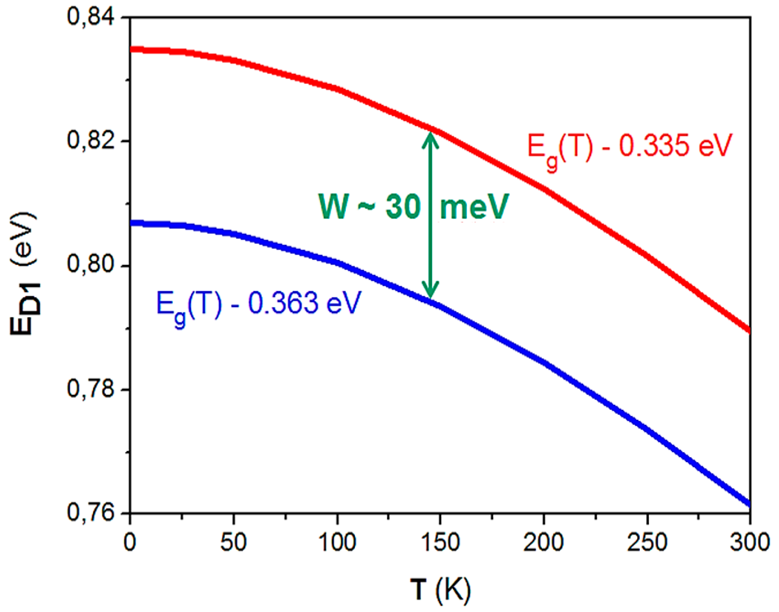
Figure 23.
Impact of misorientation/structure on the luminescence spectra of dislocation networks: (A) twist angle of ϑtwist = 3°, dominating D1 peak; and (B) twist angle of ϑtwist = 8.2°, dominating D3 peak. The same tilt angle of ϑtwist = 0.2° exists in both cases [108].
Figure 23.
Impact of misorientation/structure on the luminescence spectra of dislocation networks: (A) twist angle of ϑtwist = 3°, dominating D1 peak; and (B) twist angle of ϑtwist = 8.2°, dominating D3 peak. The same tilt angle of ϑtwist = 0.2° exists in both cases [108].

Figure 24.
(a) Schematic band diagram of a MOS-LED with thin tunneling oxide and a dislocation network close to the Si/oxide interface. (b) Electroluminescence spectra at 80 K of the MOS-LED with 1.5 µm radiation caused by the network. The intensity is found to increase sub-linearly with increasing tunneling current measured at 2, 5 and 8 mA, respectively. (c) TEM cross-section of the MOS-LED consisting of a 134 nm Ti layer on 1.8 nm Si oxide. The network is positioned in ~45 nm depth.
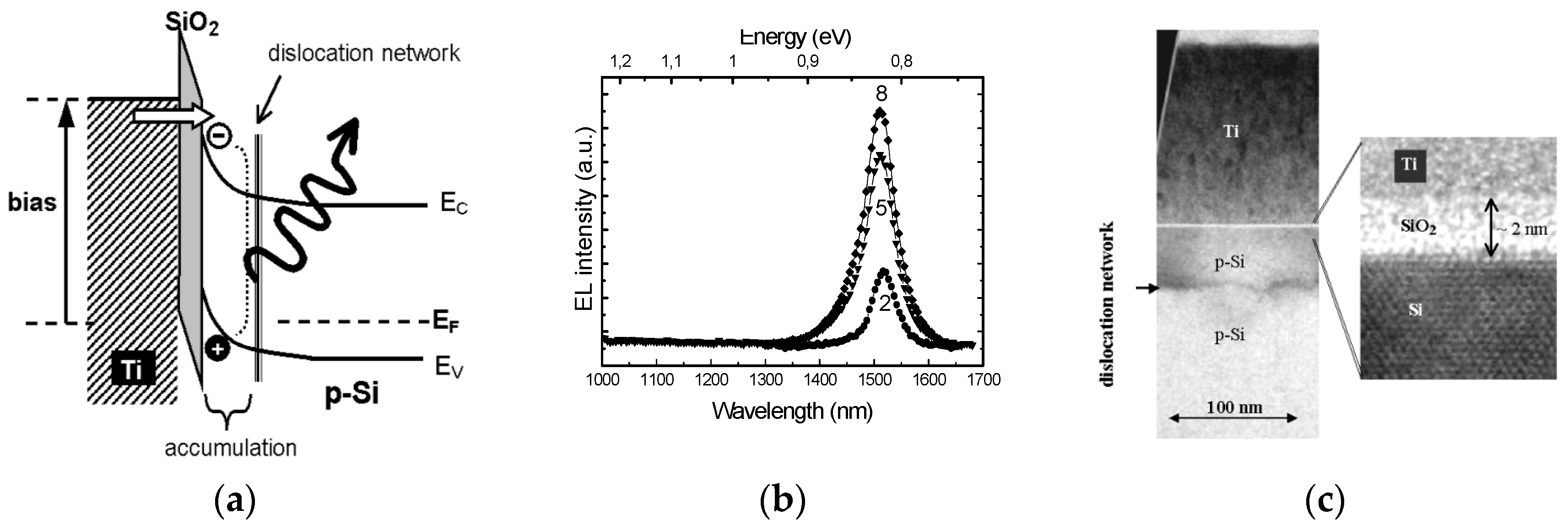
Figure 25.
Scheme of the two-electrode all silicon LED integrated in a SOI layer containing a dislocation network. As electrodes two p–n junctions are used. They are located at a distance of 2 μm within the 80 nm thick SOI layer. The EL spectrum was observed at 300 K for a forward current of 60 mA. The emission is strong and can already be detected at current of few mA by a simple panchromatic camera-based system.
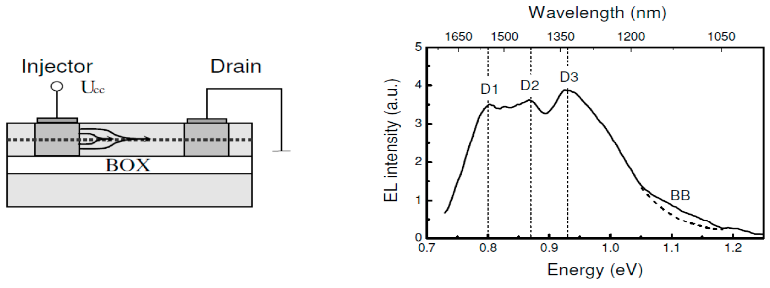
Figure 26.
Schema of the wafer bonding process. Two <100>-oriented SOI wafers are used (left), where the blue color characterizes the thin device layer (30 nm thick), yellow the buried oxide and grey the substrate wafer. Both wafers are stuck (bonded) together, so that the surfaces of both device layers are in contact (middle). A new SOI wafer results after removing one of the original substrate wafers (right). The thickness of the device layer is now 60 nm.
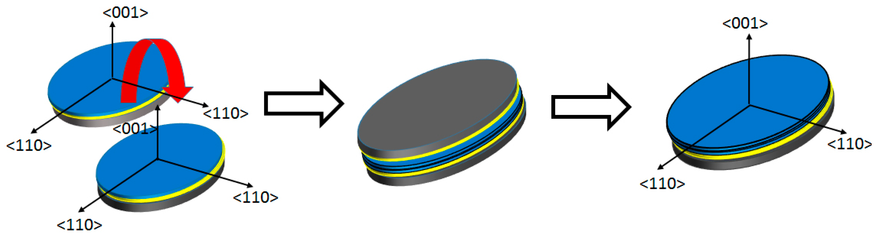
Figure 27.
Schema of an n+pn+ diode structure with a dislocation (red line) in the channel (c). Devices are fabricated parallel to <110> directions, i.e., parallel to the dislocation line direction.
Figure 27.
Schema of an n+pn+ diode structure with a dislocation (red line) in the channel (c). Devices are fabricated parallel to <110> directions, i.e., parallel to the dislocation line direction.

© 2016 by the authors; licensee MDPI, Basel, Switzerland. This article is an open access article distributed under the terms and conditions of the Creative Commons Attribution (CC-BY) license (http://creativecommons.org/licenses/by/4.0/).
Share and Cite
MDPI and ACS Style
Reiche, M.; Kittler, M. Electronic and Optical Properties of Dislocations in Silicon. Crystals 2016, 6, 74. https://doi.org/10.3390/cryst6070074
AMA Style
Reiche M, Kittler M. Electronic and Optical Properties of Dislocations in Silicon. Crystals. 2016; 6(7):74. https://doi.org/10.3390/cryst6070074
Chicago/Turabian StyleReiche, Manfred, and Martin Kittler. 2016. "Electronic and Optical Properties of Dislocations in Silicon" Crystals 6, no. 7: 74. https://doi.org/10.3390/cryst6070074
Note that from the first issue of 2016, this journal uses article numbers instead of page numbers. See further details here.