
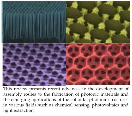
Bottom-Up Assembly and Applications of Photonic Materials


CNRS, University of Bordeaux, CRPP, UPR 8641, F-33600 Pessac, France
*
Author to whom correspondence should be addressed.
Crystals 2016, 6(5), 54; https://doi.org/10.3390/cryst6050054
Submission received: 12 April 2016
/
Revised: 4 May 2016
/
Accepted: 9 May 2016
/
Published: 12 May 2016
(This article belongs to the Special Issue Colloidal Crystals)
Abstract
:The assembly of colloidal building-blocks is an efficient, inexpensive and flexible approach for the fabrication of a wide variety of photonic materials with designed shapes and large areas. In this review, the various assembly routes to the fabrication of colloidal crystals and their post-assembly modifications to the production of photonic materials are first described. Then, the emerging applications of the colloidal photonic structures in various fields such as biological and chemical sensing, anti-reflection, photovoltaics, and light extraction are summarized.
1. Introduction
The building, manipulating, and characterizing of optically active nanostructures are related to the field of nanophotonics. By investigating the fabrication techniques and resulting material properties, we can aim to design new capabilities in instrumentation for the nanoscale, chemical and biomedical sensing, disease treatment, enhanced solar cells and lighting, information and communications technologies, and many other applications.
The basic concepts of photonics have been known for the last 40 to 50 years, but it is only in the last decade where they have really attracted attention from the scientific community based on discoveries in nanoscience. Since the 1960s, photonic materials and devices have played a pervasive role in communications, energy conversion, and sensing. Nanophotonics, or photonics at the nanoscale, can be defined as “the science and engineering of light-matter interactions that take place on wavelength and subwavelength scales where the physical, chemical, or structural nature of natural or artificial nanostructure matter controls the interactions” [1]. In the next decade, nanophotonic structures and devices hold promise in reducing the energies of device operations, enhancing the spatial resolution for imaging, creating new sensors with increased sensitivity and specificity, and creating densely integrated information systems with lower power dissipation.
Advances in the fabrication of optical structures at the nanoscale and improved control of materials properties have allowed researchers to demonstrate and realize the potential of nanophotonics, and this provides a strong motivation to continue the investigations in this fields which could further the understanding about the nature of
light-matter interactions [2].
While the fabrication of photonic nanostructures have traditionally been dominated by top-down lithography techniques, recent advances in the past decades has shown new light on the scalability and ease of using bottom-up assembly approaches to construct large arrays of homogeneous nano-patterned surfaces and materials. In addition, the relatively low cost of bottom-up assembly methods compared with top-down fabrication approaches have made the field of bottom-up assembly very accessible to a large number of research groups. With the large volumes of research work that is being churned out in this field, it is difficult to compile everything into one review paper. Hence, this review is a selective compilation of some of the published works available.
In this review, we will start by providing a conceptual overview of photonic crystals, followed by a description of the various strategies that have been developed to fabricate them, with a focus of bottom-up colloidal assembly techniques. We will also give an overview of post-assembly modifications that can be done on the assembled colloidal crystals to use them as templates for the production of photonic materials with unique patterns and morphologies. The applications of the photonic materials made by bottom assembly will be reviewed in the last section where we will discuss about how they can be used to manage photons in photovoltaics, in light emitting diodes (LEDs) and for use as sensors.
The presented material is not exhaustive but should be sufficient for the reader to grasp the general methodologies available today for the fabrication of these colloidal photonic materials and the associated applications described in this review. Earlier reviews by other authors, which have focused on different aspects of the physical properties, fabrication and applications colloidal crystals, can be read for more information [3,4,5,6,7,8,9,10,11,12,13,14,15,16].
2. Concepts
A crystal, by convention, is a periodic arrangement of atoms and molecules. The pattern with which atoms or molecules are repeated in space is the crystal lattice. The conduction properties of a crystal are determined by the constituents of the crystals as well as the geometry of the lattice, which presents a periodic potential to an electron passing through it. According to quantum mechanics, electrons travel as waves in a conducting crystal, and only the waves that meet a certain criteria can propagate through a periodic potential without scattering (in the absence of defects and impurities). At the same time, the lattice also prohibits the propagation of other waves, and this referred to as gaps in the energy band structure of the crystal. Energy bandgaps forbid the propagation of electrons with certain energies and directions. A complete bandgap occurs when there is a strong lattice potential and the gap can cover all possible propagation directions. An example is the energy band gap between the valence and conducting bands in semiconductors.
A similar analogy can be said about photonic crystals. In the case of photonic crystals (Figure 1), the “atoms or molecules” are replaced by macroscopic materials with differing dielectric constants, and the periodic potential is replaced with a periodic dielectric function (i.e., a periodic index of refraction). When the difference in dielectric constants is sufficiently large, and there is minimal absorption of light, then the refractions and reflections of light from all the various interfaces can result in a similar phenomenon for photons (light modes) that the atomic potential produces for electrons (Figure 2). Thus, a photonic crystal, a low loss periodic dielectric medium, can in theory provide a means of optical control and manipulation [16]. The position of the bandgap can be shifted by either changing the properties of the materials and/or by changing the lattice constant, while the width of the bandgap can be widened by increasing the difference between the dielectric constant of the two materials. In 1987, Yablonovitch [17] and John [18] theoretically predicted that high refractive index contrast 3D photonic crystals were capable of possessing an omnidirectional photonic bandgap, forbidding light propagation for all directions and all polarizations.
3. Fabrication Approaches
3.1. Top-Down vs. Bottom-Up
The spike in the interest and research on the photonics over the last decade has been boosted by various factors, including the significant advances in computational design tools and their accessibility, the emergence of new nanofabrication techniques, and the realization of new optical and structural characterization methods. Undoubtedly, the most important factor has been the progress in the area of fabricating photonic devices that have dimensions on the order of or below the wavelength of light [2]. For example, in order for a photonic crystal to have applications in the visible or near infrared (NIR) regimes, they would need to have spatial modulations of the refractive index of a few hundred nanometers to one micron, since the working range of a photonic crystal is directly related to the spatial periodicity of the refractive index. Fabrication techniques at this scale have traditionally been an enormous challenge in the past, and even with the current technology available and the introduction of new fabrication techniques, it still remains a challenge to discover a cost effective, reproducible, large scale and precise approach to fabricating such structures.
Fabrication of synthetic (i.e., man-made) photonic materials can be generally categorized by one of two approaches: top-down or bottom-up. Top-down approaches, such as lithography techniques using electrons, photons, atoms and ions as well as embossing and scanning tip methodologies, offer high precision and resolution to the final structure of the photonic crystal made. However, top-down approaches are generally expensive and require a longer time to fabricate the structures over a larger area because of the serial nature of the approach. In contrast, bottom-up approaches rely on the self-driven assembly of basic building blocks into ordered periodic structures that is generally faster, cheaper and on a larger scale than top-down approaches. However, the control and precision in fabricating the structures may pale slightly when compared with top-down approaches. Nonetheless, the lower cost and ease of fabrication makes bottom-up approaches offers a viable and practical alternative that could rival top-down approaches.
3.2. Colloidal Assembly
Bottom-up approaches to make photonic colloidal crystals commonly make use of spherical beads or, more rarely, anisotropic particles as building blocks for self-assembly. Typically, these particles are either silica or polystyrene (PS) latex particles because of their ease of synthesis. Monodisperse anisotropic particles have been rarely used to fabricate colloidal crystals [19,20].
The bottom-up assembly of a colloidal crystal is self-driven, implying that there are colloidal forces at work that brings the tiny building blocks together. In colloidal assembly, these forces are crucial and there are three types of forces that should be highlighted. The first type is the presence of intrinsic driving forces for ordering which could be the entropically favorable packing of monodisperse colloids into ordered arrays. For this, the monodispersity of the particles (i.e., size and shape homogeneity) is crucial. The second type to consider is the long range external forces, such as gravity or centrifugation, which act to bring the particles together. The third type is the repulsion forces between particles to prevent premature aggregation that could arise from Van der Waals forces. Electrostatic repulsions [21] by charge stabilization in polar solvents and steric repulsions [22] by solvated absorbed layers are two examples for these kind of repulsion forces.
There is a variety of assembly methods available in literature [3,7,13,23] for the fabrication of colloidal crystals depending on, the type of building blocks used, the resulting structure (two-dimensional monolayers or three-dimensional bulk crystals), and the application it is aimed at. Table 1 lists the common methods that are used to fabricate colloidal crystals.
The simplest and most basic method of direct assembly onto a substrate is by sedimentation, which is the process by which natural opals are formed as a result of gravity on the tiny individual particles that build the opal [24]. Another simple method is by drop casting. In this case, a drop of colloidal suspension is literally dropped onto the substrate surface and allowed to dry by evaporation [25]. As water evaporates, the receding meniscus helps to pull the particles together and they rearrange themselves in the lowest surface energy configuration. Temperature and humidity control, suspension concentration, choice of substrates are some of the factors that can be adjusted to obtain higher quality colloidal crystals.
Centrifugation and spin-coating are two methods that require the use of centrifugational forces to help compact the particles in a colloidal suspension. For centrifugation, a colloidal suspension in placed in a centrifuge and spun at high speeds to compact the particles together. This results in bulk colloidal crystals that are of very good quality [29]. Spin coating on the other hand, is used to make thin films or monolayers of colloidal crystals on planar substrates [30,31]. However, as the force experienced by the suspension on different parts of the substrate is different, the resulting colloidal crystal films formed on the substrate vary according to the position from the rotation axis (as illustrated in Figure 3). The colloidal crystal films are usually patchy across the substrate. Nonetheless, Jiang and co-workers have developed a robust, simple, and cost effective spin-coating technology that is scalable and compatible with standard top-down microfabrication [52]. Furthermore, they have also demonstrated the possibility to fabricate non close packed 2D colloidal crystal arrays by spin-coating [34,35].
The vertical deposition method (Figure 3) also involves evaporation of the liquid phase of a colloidal suspension to induce the convective assembly of a colloidal crystal onto a substrate. However, unlike drop casting where the substrate lays horizontal, the substrate is held vertically (or at a slight angle) and partially submerged in a colloidal suspension [26,27,53]. This method requires very good control of the deposition conditions and environment (suspension concentration, type of solvent, temperature, humidity, ground vibrations, wind, etc.), and long deposition time of a few days to allow for all the liquid (usually water) to evaporate. Any interruptions during the drying process will severely affect the quality of the colloidal crystal obtained. Nonetheless, if done correctly, very high quality of colloidal crystals can be obtained by this method. Cai et al. further demonstrated the possibility of fabricating two-dimensional non-close packed colloidal crystals using a combination of polystyrene spheres and tetraethylorthosilicate sol [54].
Dip coating involves the controlled withdrawal of a substrate from a colloidal suspension [36,37,38]. The substrate is vertically held on one end and first submerged into a colloidal suspension. It is then slowly pulled up from the suspension, and convective assembly takes place at the interface between the substrate surface and the air/liquid interface (the phenomenon is similar to vertical deposition). The thickness of the colloidal crystal deposited can be tuned by adjusting the speed of substrate withdrawal. Shear ordering makes use of a narrow channel between two planes to confine and induce packing of the particles in a colloidal suspension by shear forces [39]. This method is difficult to perform because of the complexity in maintaining a uniform shear force throughout the process.
The Langmuir-Blodgett (LB) technique is slightly different compared with the abovementioned methods. The previous methods involved the fabrication of colloidal crystals directly onto the substrates, while the Langmuir-Blodgett technique is a two-step process whereby a two-dimensional colloidal crystal monolayer is first formed on a water surface before it is transferred onto the substrate [41,44,55]. The monolayer of particles is formed by first spreading a colloidal suspension onto the surface of water and then followed by compacting the particles on the water surface by using mobile arms, while at the same time monitoring the surface pressure to determine when the monolayer is closed packed. The direct interfacial self assembly of colloidal particles on the water surface transfer method is similar to the Langmuir-Blodgett technique in the sense that particles are spread on a water surface, but it differs in that, unlike the Langmuir-Blodgett technique, the particles self-organize into closed pack arrays by tuning the surface tension of water with surfactant, instead of physical compression using mobile arms [45,46,56]. Recently, Gao et al. reported the use of the interfacial self assembly process to cover 1 m² glass substrate with a monolayer of polystyrene spheres, highlighting the immense scalability of the process (Figure 4) [48]. In addition, Langmuir-Blodgett and interfacial self assembly allows the possibility of stacking individual 2D layers on top of each other, thus giving the possibility to create (2 + 1)D type of colloidal crystals (Figure 4) [41,44,47,57]. Oh et al. described a simple method for fabricating wafer scale colloidal crystal film of 2D crystals in a 1D stack by combing the processes of self-assembly of polystyrene beads at the air-water interface and the layer-by-layer scooping transfer technique [47]. Recently, Zhang et al. reported the flexible control in structure and stop band position of (2 + 1)D photonic crystal superlattices by stacking of colloidal monolayers with different diameters of polystyrene (Figure 4) [57].
The use of magnetic self-assembly of paramagnetic colloidal particles is another unique of fabricating colloidal photonic crystals. The main requirement here is the use of highly charged, monodisperse superparamagnetic colloidal particles. Due to their highly charged nature, the colloidal particles have a tendency to self-assemble into ordered arrangements that have the possibility to be controlled by external magnetic fields. Several related works on this subject have been reported by Asher et al., demonstrating the different synthesis routes to make such colloidal particles and their subsequent self-assembly [49,50,51].
4. Post-Assembly Modification
4.1. Nanosphere Lithography
The term “nanosphere lithography” was first coined by Van Duyne and co-workers two decades ago [58]. Today, nanosphere lithography is a well-known technique used to produce homogeneous and regular arrays of nanoparticles of various sizes [59,60]. In general, nanosphere lithography involves the preparation of a template consisting of a hexagonal close packed monolayer or bilayer of monodisperse spherical particles onto a substrate surface [45,61]. This is followed by either the deposition of a material into the interstitial spaces between the spherical particles [62] or the etching of the substrate using the template as a protective mask [63]. Infiltration of a desired material into the template can be done with techniques such as electron beam evaporation [64], electrodeposition [65], sol-gel [66,67], metal evaporation [68,69], and magnetron sputtering [48,70,71]. Either way, at the end of the process when the template is removed, an array of nanoparticles/nanostructures will be produced on the substrate surface.
Nanosphere lithography provides an easy control of the spacing between the nanoparticles which can be tuned by the size of the spherical particles used. Furthermore, a variety of substrates can be used and almost any type of material can be deposited into the mask. The monolayer templates can also be treated to modify the shapes of the interstitial spaces [65,68].
Several interesting nanostructures made of different materials have, so far, been demonstrated. These include, but are not limited to, nanotriangles [61,62], nanodots [61,68,72], nanopillars [63,65,69,73,74,75,76], nanorods [68], nanopyramids [64], nanorings [68,77], nanowells/bowls [67,69] and inverted nanocones [78]. Vogel et al. described a simple process of using oxgen plasma etching to modify a close packed monolayer of polystyrene beads into a non-closed packed monolayer (Figure 5) [45]. Kosiorek et al. reported the use of shadow nanosphere lithography to prepare two-dimensional metallic nanostructures such as rings, dots and rods. This was done by modifying the mask morphology via temperature processing and by varying the evaporation conditions (Figure 6) [68].
Zhang et al. described the use of a combination of nanosphere lithography combined with chemical deposition and a subsequent physical deposition step with a careful control of each step to create various types of novel nanostructured arrays resembling honey-combs, hollow cavities and regular network arrays [71,79]. Wang et al. reported the use of nanosphere lithography to manufacture titanium dioxide nanobowl structures that were used to further grow titanium dioxide nanorods in them for photoelectrical water splitting purposes [67]. Hang et al. reported a method to fabricate uniform copper nanosphere arrays over a large scale by sputtering copper through monolayer colloidal crystal templates [72]. Tabatabaei et al. made use of nanosphere lithography to deposit silver and gold tetrahedral pyramids onto ITO (indium tin-doped oxide) and glass surfaces. They succeeded in making 3D nanopyramids of 350–400 nm in height (Figure 7) [64]. Recently, Zheng et al. reported the use of electrodeposition and nanosphere lithography to fabricate self-standing gold nanopillar arrays that could subsequently be transferred onto a polydimethylsiloxane (PDMS) substrates (Figure 7) [65].
Overall, nanosphere lithography is a relatively quick and simple way to create a homogeneous pattern across a large surface area. Even though nanosphere lithography suffers from slight imperfections due to the nature of the technique, the simplicity and speed of using this technique makes it a viable alternative to traditional top-down lithography techniques when patterning a large area.
4.2. Inverse Opals
Inverse opals (also known as inverted opals or three-dimensionally ordered macroporous (3DOM) materials) are the inverse replicas of a self-assembled colloidal crystal. They can be fabricated by the infiltration of the colloidal crystals with a desired material and subsequently removing the template. An interesting property of inverse opals is that they can theoretically exhibit a complete photonic bandgap (cPBG), if the difference in the refractive index of the constituent materials is sufficiently high enough [80]. Due to their ability to “manage” light over the range of its bandgap [81,82,83], inorganic semiconductor materials such as titania [84,85,86,87,88,89], silica [90,91,92,93], and zinc oxide [94] have all been made into inverse opals and studied extensively. In addition, other materials such as metals [42,80,95,96,97,98,99,100] and organic materials [101,102,103,104,105] have also been fabricated into inverse opals and investigated.
There are various methods available for the infiltration process depending of the material desired. These methods include, but are not limited to, atomic layer deposition [106,107,108,109], chemical vapor deposition [11,84,108,110], electrochemical deposition [97,111,112,113,114], and sol-gel techniques (Figure 8) [85,87,91,93,115,116].
Cai et al. demonstrated an improved convective self-assembly technique to fabricate composite heterostructures, and they showed that they could fabricate both opaline and inverse opaline heterostructures with long range ordering (>100 × 100 µm²) [93]. Alessandri et al. reported the fabrication of inverse opal CeO2/TiO2 core-shell structures with precisely defined architectures and pore size by combining colloidal crystal templates with atomic layer deposition. Recently, Kim et al. reported the successful fabrication of a silk inverse opal, a three-dimensional inverse opal photonic crystal made entirely of purified silk fibroin, a natural protein (Figure 9) [101]. In general, inverse opals are an interesting class of materials because of their relative ease of fabrication and the unique physical and optical properties associated with their structure.
In the following section, we will discuss about some of the applications associated with the nanostructured photonic materials that can be derived from the bottom-up colloidal assembly process.
5. Applications
5.1. Photon Management in Photovoltaics
The use of photonic structures to manage light and optimize optical and electro-optical properties in photovoltaic devices has been widely studied [117,118,119,120,121,122]. Photonic structures can enable the “trapping” of photons and consequently enhance the photocurrent of a solar cell [120]. Suezaki et al. reported that boron and phosphorous doped inverse opal silicon solar cells made by self-assembly methods demonstrated acceptable performances for device applications [123]. Using nanosphere lithography, Zhang et al. showed the possibility to create ordered arrays of silicon pillars by reactive ion etching of 2D polystyrene arrays [63]. Garnett et al. demonstrated the fabrication of silicon nanowire solar cells made by ion etching of monolayers of silica beads through a self-assembly process. They reported that the ordered arrays of silicon nanowires increased the path length of incident solar light radiation by up to a factor of 73 (Figure 10) [75]. Chen et al. demonstrated a surface texturing “bottom-up” technique to spread silica microspheres onto the surface of a silicon solar cell resulting in a superior omnidirectional anti-reflection property of silicon solar cells. They reported an increase in the effective area for carrier collection and efficiency of the cells [124]. Zhang et al. demonstrated the fabrication of inverted silicon nanocone arrays that exhibited broadband light anti-reflectance properties [78].
Yao et al. demonstrated a new approach to light management by forming whispering-gallery resonant modes inside a spherical nanoshell structure that was based upon a silica colloidal crystal made by the Langmuir Blodgett technique. They reported a broadband absorption enhancement across a large range of incident angles with their designed nanocrystalline silicon model system (Figure 11) [125].
Certain porous metallic materials made via self-assembled spherical particles could also be interesting for light management in photovoltaics [97,98,126,127]. By electrodepositing gold into a monolayer of close packed polystyrene particles, Teperik et al. reported that total absorption of light can be achieved in nanostructured metal surfaces that sustain localized optical excitations [98,126]. In their work, they reported that by controlling the thickness of gold just slightly above the particles, there is an optimum thickness resulting in total absorption of incident light. In addition, they also theoretically predicted possible omnidirectional absorption of light in such structures [98]. Recently, Zheng et al. investigated the total omnidirectional light absorption properties of such porous gold surface and confirmed experimentally the possibility of this phenomenon. They reported the observation of quasi-omnidirectional total absorption of light on their fabricated surfaces as well as the tunability of the absorption wavelength by varying the size of the spheres. The strongly enhanced absorption was observed for angles of incidence up to 65° (Figure 12) [97]. A separate study on the quality of the electrodeposited gold was also reported [128].
The use of self-assembled colloidal crystals in dye sensitized solar cells (DSSCs) has also drawn much interest in recent years [106,108,129,130,131,132,133]. DSSCs are an interesting alternative to conventional solid state semiconductor photovoltaic devices largely due to their low cost of production [134]. Miguez and co-workers made theoretical investigations on the effect of the presence of a photonic crystal on the optical absorption of DSSCs. They concluded that significant light absorption amplification over a wide spectral range occurred in structures that combined the presence of a photonic crystal and a layer of nanocrystalline absorbing material, and that the absorption enhancement occurs in resonant modes localized within the absorbing nanocrystalline coating [83]. In addition, it was predicted that the piling up of different lattice constant crystals can lead to light harvesting enhancement in the whole dye absorption range [82]. Several strategies have since been developed to combine photonic crystals and DSSCs by self-assembly techniques. Zhang et al. demonstrated the use of photonic crystal concentrators for DSSCs made by self-assembly of latex spheres on concave watch glasses. They concluded that the wavelength selective photonic crystal concentrator can improve the maximum power of the DSSC by more than five times while retaining a stable high performance (Figure 13) [135].
Somani et al. reported the fabrication of solid state DSSC with titania inverse opal films to increase the efficiency of the cells. They claimed that the ordered interconnected cavities forming the microporous structure allow the easy penetration of both the dye and the solid-state hole conductor material, which favors the intimate contact of both these elements through the whole depth of the titania [131]. Lee et al. did a similar experiment with liquid DSSCs that contained bilayers of nanocrystalline titania and titania inverse opals. They report that the efficiency enhancement is very sensitive to the degree of physical contact between the two layers [132]. Guldin et al. presented a material assembly route to fabricate DSSCs with titania inverse opals which involved the vertical deposition of polystyrene spheres onto FTO glass substrates. They attributed the increase in the photocurrent of such cells to the multidirectional scattering of short wavelength photons due to defects in the photonic crystal layer, back reflection of light in the stop band region of the photonic crystal due to the photonic crystal layer acting as a dielectric mirror, and an absorption enhancement caused by resonant modes [110]. Seo et al. reported the use of an induced accelerated solvent evaporation process during colloidal self-assembly to rapidly fabricate titania inverse opal photoelectrodes for DSSCs (Figure 14). They reported that their titania inverse opal films exhibited a reliable light modulation at reflectance mode. Furthermore, when used as a DSSC photoelectrode, a relatively high conversion efficiency of 4.2% was obtained [133].
Mihi et al. proposed a procedure to separately fabricate the titania inverse opal before transferring into the DSSC device (Figure 15). They demonstrated that their preformed 3D photonic crystals can be applied onto a diverse set of surfaces. More importantly, they reported the an enhanced light trapping in DSSCs by coupling a porous photonic crystal film to both zinc oxide nanowire and nanocrystalline titanium dioxide DSSC electrodes [108].
Hwang et al. presented a design which integrated the nanocrystalline titania underlayer with the optically active porous photonic crystal layer, along with a sequential infiltration process to introduce additives into the solid electrolyte of the DSSC (Figure 16). Their design yielded an enhanced absorption in specific spectral regions and they reported an improved performance of the fabricated DSSCs by as much as 32% as compared with conventional DSSCs [136]. Recently, Lee et al. reported the use of a plate-sliding coating method coupled with hot air flow to deposit mesoscale colloidal crystals which were then infiltrated with titania by atomic layer deposition (ALD) to create titania inverse opals with 70 nm pores. They also claimed that these type of photo-electrochemical electrode exhibited enhanced charge transport properties and high specific surface area [106].
5.2. Light Emitting Diodes
While photonic nanostructures can be used to “trap” light to increase the absorption in photovoltaic devices, they can also used to extract light from light emitting devices (LEDs). Hsieh et al. reported a fabrication approach to texture gallium nitride (GaN) LEDs by nanosphere lithography. They describe the use of spin-coating to texture the LEDs with a monolayer of silica nanoparticles. Their results show that textured p-GaN and indium tin oxide LEDs exhibit significant improvements as compared to conventional LEDs with disparity in electrical characteristics [137]. Kim et al reported that arrays of silica nanosphere monolayers that were spin-casted onto a polymer layer on top of a GaN surface can result in a hexagonal pattern of nanolenses that was shown to improve the light extraction efficiency of ultra violet LEDs by 23% [138].
An et al. described the use of cone-shaped deep-pillar nanostructures to improve light extraction in Honeycomb-type vertical GaN light emitting diodes (VLEDs). The cone-shaped pillar patterns were made by spin-coating polystyrene nanospheres onto n-GaN substrates and subsequently etching the surface under oxygen plasma. They reported that their structure increased the output power of VLEDs by up to 214% at 350 mA versus a reference device, and they attributed this to the multiple light scattering from the sidewalls of the cones (Figure 17) [139].
Li et al. described the use of nanosphere lithography to pattern a close-packed array of nanopillars that is embedded within an InGaN/GaN LED structure. The periodic ordered nanopillar structure promotes light extraction and at the same time suppresses the piezoelectric field through strain relaxation of the InGaN/GaN quantum wells. They reported that the LEDs with the embedded photonic crystals exhibit as much as 20% more light than the reference LED (Figure 18) [140]. Dylewicz et al. reported that the random surface texturing on a gallium nitride (GaN) LED wafer by a mask-less dry etch process could result in an increased light extraction capability from within the epilayers. Their process involves the deposition of monolayer of silica particles, which are then subjected to a dry etching process to create fragments that randomly deposit on the GaN surface. These fragments then serve as a mask when the substrate is exposed to dry plasma etching where the exposed GaN surface will be etched away [141]. Ng et al. made use of nanosphere lithography to create a hexagonal array of air holes by dry etching a self-assembled silica monolayer on a GaN surface. They reported a twofold enhancement of the light emission from the fabricated LEDs with the photonic crystal. This increase was attributed to the light dispersion of the photonic crystal, light diffraction through the photonic crystal grating and the scattering of light due to the roughened surface [142].
5.3. Sensors
The photonic bandgaps and structural colors of self-assembled colloidal crystals are directly dependent on the structure and nature of the component materials. Hence, this property makes them suitable as materials for use in sensing technologies. Fenzl et al. published several works on the use of photonic crystal as sensors for sensing ionic strength [143], potassium ions [144], organic solvents in water [145], and acetylcholine/acetylcholinesterase inhibitors [146]. Hoi et al. reported a technique to fabricate photonic chips that can integrate colloidal crystals, optical fibres and microfluidic channels for lab-on-a-chip devices. They reported the tunability of their filters by modifying the type of colloidal crystals used [147]. Xu et al. made use of colloidal crystal arrays to fabricate three-dimensional periodic voids in hydroxyethyl methacrylate polymerized crystalline colloidal array (HEMA PCCA). This was used to monitor ethanol concentration in water which directly affected the diffraction wavelength [104]. Li et al. demonstrated the use of inverse opals as oil sensors. They described the reversible shifting of the stop-band which varies as a linear function of the refractive index of the adsorbed oil [103]. Zhang et al. described the development of a sensing material made of a crystalline 2D array of colloidal photonic crystal. They reported the use of this sensing material for the visual determination of surfactants and that the sensitivity of this material can be increased by incorporating hydrophobic monomers (Figure 19) [148].
Xu et al. developed a spherical porphyrin sensor array based on colloidal crystals for volatile organic compounds (VOC) vapor detection. They described that different VOC vapors can be discriminated by observing the change in fluorescence color of the porphyrin-modified colloidal crystals. In addition, the reflection peaks of the colloidal crystals serve as the encoding signal for different sensors (Figure 20) [149]. Lu et al. reported the fabrication of metal organic framework (MOF) containing silica colloidal crystals for sensing volatile molecules. They combined MOFs with thin film colloidal crystals to overcome the problem of signal transduction during molecular sorption. They reported the readily observable shifts in the colloidal crystal stop bands during analyte sorption by the MOFs [150]. Using polydimethylsiloxane and a 3D colloidal crystal, Endo et al. reported a chemical sensing device for VOC that demonstrated colorimetric detection capabilities. Their device allowed the detection of the type and concentration of the VOC, and can be easily observable with the naked eye [151].
Shin et al. reported a mechanically robust pH sensor made by templated photo-polymerization of hydrogel monomers within a self-assembled colloidal photonic crystal. They demonstrated that their photonic crystal could detect a pH change in under 10 s and that the sensors were also stable over a long periods of time with no degradation of the response time nor the reproducibility of the pH-driven color change (Figure 21) [152].
Li et al. reported a photonic crystal sensing motif that is based on a 2D inverse opal monolayer of polyelectrolyte gel. Their sensor is described to be responsive to pH changes and can be readily interpreted from the interference colors or its optical spectra [153]. Honda et al. developed a synthetic colorimetric glucose-sensing system based on glucose-responsive hydrogel particles embedded in an inverse opal polymer membrane. Their system is capable of producing a reversible change in color due to the change in the volume of the hydrogel particles as a result of a change in glucose concentration. They claim that a careful design of the system can allow the diagnosis of diabetes mellitus [154]. Huang et al. fabricated 3D macroporous pH-responsive polymers by using silica colloidal crystals as templates. They reported the swelling and de-swelling of the macroporous polymer films due to external stimuli, which causes a change in the Bragg diffraction of the material. This allowed the detection of pH or ionic strength of various solutions by optical signals [155]. Griffete et al. fabricated inverse opal hydrogels containing a planar defect which allowed the detection of a pH variation in less than 10 s [156]. The same authors used colloidal crystals of silica particles that were built by the Langmuir-Blodgett technique as templates to elaborate inverse opal films of molecularly imprinted polymers. The inverse opals were found to display large responses to external stimuli (pH or bisphenol A) with Bragg diffraction peak shifts depending upon the hydrogel film thickness [157,158]. Cai et al. fabricated a two-dimensional photonic crystal protein hydrogel sensor for selective detection of the fungal pathogen Candida albicans. They made use of the shrinking of the hydrogel when exposed to the pathogen to modify the particle spacing in the 2D array, which translated to visually evident blue shifts of diffracted light that could be readily detected. The sensor is a proof of concept for utilizing recognition between microbial cell surface carbohydrates and lectins to detect microorganisms in aqueous environments [159]. Men et al. reported that optical sensors based on hydrogel films with 2D colloidal arrays on both surfaces exhibited enhanced diffraction intensity and avoided the curling problems on traditional hydrogel films with only a single colloidal array on one side [160]. They further reported that the use of 2D gold nanosphere array on a hydrogel film displayed a stronger diffraction intensity due the periodicity and larger scattering cross section of gold nanospheres. This type of 2D gold nanosphere/hydrogel composite films could potentially be used for visual determination of an analyte [161].
The ability to respond to external stimuli and convert that information into visible signals makes colloidal photonic crystal based sensors ideal for real life biosensing applications. Furthermore, the various different types of materials that can be used and the corresponding environments they are used in provide a high degree of configurability and adaptability to usage specific sensing applications.
6. Conclusions
The development of bottom-up assembly techniques has progressed significantly over the last few decades. Improvements in the quality of the self-assembled structures, the increased scalability of the processes and the shortening of the time required to prepare these materials have been pivotal for their adaptations into novel applications.
With the inevitable growth of solar photovoltaic technologies, in light of the impending energy crisis, there is a pressing need for photonic technologies that can be adapted to a large scale at low cost for higher efficiency devices. The bottom fabrication of self-assembled photonic crystals and the associated materials and structures that can be derived from them are perfectly positioned in this respect. Fabrication of nanostructured materials that are able to manage light will be a key determinant of the success of future photovoltaic technologies, as this technology is currently being held back mainly because of the associated cost. At the same time, the use of colloidal photonic crystals for the extraction of light from light emitting devices is also significant in the race to create lower energy consumption and higher energy efficiency devices, without suffocating the technology with excessive costs. The use of colloidal photonic crystal for sensing technologies is also a very promising field for the future. The ease of detection of various compounds simply by observing the change in color of the sensor makes it a powerful tool that can be easily applied in various situations.
In this review, we have covered the concepts and recent advancements in bottom-up self-assembly processes to make 2D and 3D colloidal photonic crystals. We have explored some of the possibilities of using self-assembled colloidal crystals as templates for fabricating inverse opals and for nanosphere lithography. Furthermore, we have highlighted three domains of applications where the use of bottom-up assembled colloidal crystals can be very useful.
We hope that this review has provided a clear introduction into the field of bottom-up self assembled colloidal crystals for anyone new to this field and at the same time provided new insights and ideas for the seasoned researchers in this field. Even though there still remains a lot more to be discovered, in terms of the associated physics and the chemistry of these materials, it is simply a matter of time before the next leap towards better understanding, improved fabrication technologies and innovative new applications.
Author Contributions
Hanbin Zheng and Serge Ravaine wrote the paper.
Conflicts of Interest
The authors declare no conflict of interest.
References
- Committee on Nanophotonics Accessibility and Applicability; Air Force Studies Board; Division on Engineering and Physical Sciences; National Research Council. Nanophotonics: Accessibility and Applicability; National Academies Press: Washington, DC, USA, 2008. [Google Scholar]
- Hu, E.L.; Brongersma, M.; Baca, A. Applications: Nanophotonics and Plasmonics. In Nanotechnology Research Directions for Societal Needs in 2020; Springer: Dordrecht, The Netherlands, 2008; pp. 318–340. [Google Scholar]
- Cong, H.; Yu, B.; Tang, J.; Li, Z.; Liu, X. Current status and future developments in preparation and application of colloidal crystals. Chem. Soc. Rev. 2013, 42, 7774–7800. [Google Scholar] [CrossRef] [PubMed]
- Galisteo-Lõpez, J.F.; Ibisate, M.; Sapienza, R.; Froufe-Pérez, L.S.; Blanco, Ú.; Lõpez, C. Self-assembled photonic structures. Adv. Mater. 2011, 23, 30–69. [Google Scholar] [CrossRef] [PubMed]
- Ge, J.; Yin, Y. Responsive photonic crystals. Angew. Chem. Int. Ed. 2011, 50, 1492–1522. [Google Scholar] [CrossRef] [PubMed]
- Kim, S.-H.; Lee, S.Y.; Yang, S.-M.; Yi, G.-R. Self-assembled colloidal structures for photonics. NPG Asia Mater. 2011, 3, 25–33. [Google Scholar] [CrossRef]
- Li, F.; Josephson, D.P.; Stein, A. Colloidal assembly: The road from particles to colloidal molecules and crystals. Angew. Chem. Int. Ed. 2011, 50, 360–388. [Google Scholar] [CrossRef] [PubMed]
- Li, J.; Zheng, T. A comparison of chemical sensors based on the different ordered inverse opal films. Sens. Actuators B Chem. 2008, 131, 190–195. [Google Scholar] [CrossRef]
- López, C. Materials aspects of photonic crystals. Adv. Mater. 2003, 15, 1679–1704. [Google Scholar] [CrossRef]
- Stein, A.; Wilson, B.E.; Rudisill, S.G. Design and functionality of colloidal-crystal-templated materials—Chemical applications of inverse opals. Chem. Soc. Rev. 2013, 42, 2763–2803. [Google Scholar] [CrossRef] [PubMed]
- Tétreault, N.; Míguez, H.; Ozin, G.A. Silicon inverse opal—A platform for photonic bandgap research. Adv. Mater. 2004, 16, 1471–1476. [Google Scholar] [CrossRef]
- Vogel, N.; Weiss, C.K.; Landfester, K. From soft to hard: The generation of functional and complex colloidal monolayers for nanolithography. Soft Matter 2012, 8, 4044–4061. [Google Scholar] [CrossRef]
- Von Freymann, G.; Kitaev, V.; Lotsch, B.V.; Ozin, G.A. Bottom-up assembly of photonic crystals. Chem. Soc. Rev. 2013, 42, 2528–2554. [Google Scholar] [CrossRef] [PubMed]
- Ye, X.; Qi, L. Two-dimensionally patterned nanostructures based on monolayer colloidal crystals: Controllable fabrication, assembly, and applications. Nano Today 2011, 6, 608–631. [Google Scholar] [CrossRef]
- Fenzl, C.; Hirsch, T.; Wolfbeis, O.S. Photonic crystals for chemical sensing and biosensing. Angew. Chem. Int. Ed. 2014, 53, 3318–3335. [Google Scholar] [CrossRef] [PubMed]
- Joannopoulos, J.D.; Johnson, S.G.; Winn, J.N.; Meade, R.D. Photonic Crystals—Molding the Flow of Light, 2nd ed.; Princeton University Press: Princeton, NJ, USA, 2008. [Google Scholar]
- Yablonovitch, E. Inhibited spontaneous emission in solid-state physics and electronics. Phys. Rev. Lett. 1987, 58, 2059–2062. [Google Scholar] [CrossRef] [PubMed]
- John, S. Strong localisation of photons in certain disordered dielectric superlattices. Phys. Rev. Lett. 1987, 58, 2486–2489. [Google Scholar] [CrossRef] [PubMed]
- Ding, T.; Song, K.; Clays, K.; Tung, C.H. Controlled directionality of ellipsoids in monolayer and multilayer colloidal crystals. Langmuir 2010, 26, 11544–11549. [Google Scholar] [CrossRef] [PubMed]
- Ding, T.; Song, K.; Clays, K.; Tung, C.-H. Fabrication of 3D photonic crystals of ellipsoids: Convective self-assembly in magnetic field. Adv. Mater. 2009, 21, 1936–1940. [Google Scholar] [CrossRef]
- Walker, D.A.; Kowalczyk, B.; de la Cruz, M.O.; Grzybowski, B.A. Electrostatics at the nanoscale. Nanoscale 2011, 3, 1316–1344. [Google Scholar] [CrossRef] [PubMed]
- Bishop, K.J.M.; Wilmer, C.E.; Soh, S.; Grzybowski, B.A. Nanoscale forces and their uses in self-assembly. Small 2009, 5, 1600–1630. [Google Scholar] [CrossRef] [PubMed]
- Velev, O.D.; Gupta, S. Materials fabricated by micro- and nanoparticle assembly—The challenging path from science to engineering. Adv. Mater. 2009, 21, 1897–1905. [Google Scholar] [CrossRef]
- Davis, K.E.; Russel, W.B.; Glantschnig, W.J. Disorder-to-order transition in settling suspensions of colloidal silica: X-ray measurements. Science 1989, 245, 507–510. [Google Scholar] [CrossRef] [PubMed]
- Pusey, P.N.; van Megen, W. Phase behaviour of concentrated suspensions of nearly hard colloidal spheres. Nature 1986, 320, 340–342. [Google Scholar] [CrossRef]
- Zhou, Z.; Zhao, X.S. Flow-controlled vertical deposition method for the fabrication of photonic crystals. Langmuir 2004, 20, 1524–1526. [Google Scholar] [CrossRef] [PubMed]
- Fortes, L.M.; Gonçalves, M.C.; Almeida, R.M. Processing optimization and optical properties of 3-D photonic crystals. J. Non Cryst. Solids 2009, 355, 1189–1192. [Google Scholar] [CrossRef]
- Fortes, L.M.; Gonçalves, M.C.; Almeida, R.M. Flexible photonic crystals for strain sensing. Opt. Mater. 2011, 33, 408–412. [Google Scholar] [CrossRef]
- Jiang, Y.; Yang, X.; Wang, C.; Li, H.; Dong, F.; Yang, B.; Yu, K.; Lin, Q. Centrifugation-induced water-tunable photonic colloidal crystals with narrow diffraction bandwidth and highly sensitive detection of SCN. ACS Appl. Mater. Interfaces 2013, 5, 1990–1996. [Google Scholar]
- Ko, Y.G.; Shin, D.H.; Lee, G.S.; Choi, U.S. Fabrication of colloidal crystals on hydrophilic/hydrophobic surface by spin-coating. Colloids Surf. A Physicochem. Eng. Asp. 2011, 385, 188–194. [Google Scholar] [CrossRef]
- Arutinov, G.; Brichkin, S.B.; Razumov, V.F. Self-assembling of polystyrene microsphere monolayers by spin-coating. Nanotechnol. Russ. 2010, 5, 67–72. [Google Scholar] [CrossRef]
- Nandiyanto, A.B.D.; Ogi, T.; Iskandar, F.; Okuyama, K. Highly ordered porous monolayer generation by dual-speed spin-coating with colloidal templates. Chem. Eng. J. 2011, 167, 409–415. [Google Scholar] [CrossRef]
- Jiang, P.; McFarland, M.J. Large-scale fabrication of wafer-size colloidal crystals, macroporous polymers and nanocomposites by spin-coating. J. Am. Chem. Soc. 2004, 126, 13778–13786. [Google Scholar] [CrossRef] [PubMed]
- Jiang, P.; Prasad, T.; McFarland, M.J.; Colvin, V.L. Two-dimensional non close-packed colloidal crystals formed by spincoating. Appl. Phys. Lett. 2006, 89, 011908. [Google Scholar] [CrossRef]
- Jiang, P.; McFarland, M.J. Wafer-scale periodic nanohole arrays templated from two-dimensional nonclose-packed colloidal crystals. J. Am. Chem. Soc. 2005, 127, 3710–3711. [Google Scholar] [CrossRef] [PubMed]
- Armstrong, E.; Khunsin, W.; Osiak, M.; Blömker, M.; Torres, C.M.S.; O’Dwyer, C. Ordered 2D colloidal photonic crystals on gold substrates by surfactant-assisted fast-rate dip coating. Small 2014, 10, 1895–1901. [Google Scholar] [CrossRef] [PubMed]
- Ye, Y.-H.; Mayer, T.S.; Khoo, I.-C.; Divliansky, I.B.; Abrams, N.; Mallouk, T.E. Self-assembly of three-dimensional photonic-crystals with air-core line defects. J. Mater. Chem. 2002, 12, 3637–3639. [Google Scholar] [CrossRef]
- Deleuze, C.; Sarrat, B.; Ehrenfeld, F.; Perquis, S.; Derail, C.; Billon, L. Photonic properties of hybrid colloidal crystals fabricated by a rapid dip-coating process. Phys. Chem. Chem. Phys. 2011, 13, 10681–10689. [Google Scholar] [CrossRef] [PubMed]
- Amos, R.; Rarity, J.; Tapster, P.; Shepherd, T.; Kitson, S. Fabrication of large-area face-centered-cubic hard-sphere colloidal crystals by shear alignment. Phys. Rev. E 2000, 61, 2929–2935. [Google Scholar] [CrossRef]
- Hur, J.; Won, Y.-Y. Fabrication of high-quality non-close-packed 2D colloid crystals by template-guided Langmuir-Blodgett particle deposition. Soft Matter 2008, 4, 1261–1269. [Google Scholar] [CrossRef]
- Reculusa, S.; Ravaine, S. Synthesis of colloidal crystals of controllable thickness through the Langmuir-Blodgett technique. Chem. Mater. 2003, 15, 598–605. [Google Scholar] [CrossRef]
- Heim, M.; Reculusa, S.; Ravaine, S.; Kuhn, A. Engineering of complex macroporous materials through controlled electrodeposition in colloidal superstructures. Adv. Funct. Mater. 2012, 22, 538–545. [Google Scholar] [CrossRef]
- Szamocki, R.; Reculusa, S.; Ravaine, S.; Bartlett, P.N.; Kuhn, A.; Hempelmann, R. Tailored mesostructuring and biofunctionalization of gold for increased electroactivity. Angew. Chem. Int. Ed. 2006, 45, 1317–1321. [Google Scholar] [CrossRef] [PubMed]
- Reculusa, S.; Massé, P.; Ravaine, S. Three-dimensional colloidal crystals with a well-defined architecture. J. Colloid Interface Sci. 2004, 279, 471–478. [Google Scholar] [CrossRef] [PubMed]
- Vogel, N.; Goerres, S.; Landfester, K.; Weiss, C.K. A convenient method to produce close- and non-close-packed monolayers using direct assembly at the air-water interface and subsequent plasma-induced size reduction. Macromol. Chem. Phys. 2011, 212, 1719–1734. [Google Scholar] [CrossRef]
- Lu, Z.; Zhou, M. Fabrication of large scale two-dimensional colloidal crystal of polystyrene particles by an interfacial self-ordering process. J. Colloid Interface Sci. 2011, 361, 429–435. [Google Scholar] [CrossRef] [PubMed]
- Oh, J.R.; Moon, J.H.; Yoon, S.; Park, C.R.; Do, Y.R. Fabrication of wafer-scale polystyrene photonic crystal multilayers via the layer-by-layer scooping transfer technique. J. Mater. Chem. 2011, 21, 14167–14172. [Google Scholar] [CrossRef]
- Gao, P.; He, J.; Zhou, S.; Yang, X.; Li, S.; Sheng, J.; Wang, D.; Yu, T.; Ye, J.; Cui, Y. Large-area nanosphere self-assembly by a micro-propulsive injection method for high throughput periodic surface nanotexturing. Nano Lett. 2015, 15, 4591–4598. [Google Scholar] [CrossRef] [PubMed]
- Xu, X.; Asher, S.A. Synthesis and utilization of monodisperse hollow polymeric particles in photonic crystals. J. Am. Chem. Soc. 2004, 126, 7940–7945. [Google Scholar] [CrossRef] [PubMed]
- Xu, X.; Friedman, G.; Humfeld, K.D.; Majetich, S.A.; Asher, S.A. Superparamagnetic photonic crystals. Adv. Mater. 2001, 13, 1681–1684. [Google Scholar] [CrossRef]
- Xu, X.; Friedman, G.; Humfeld, K.D.; Majetich, S.A.; Asher, S.A. Synthesis and utilization of monodisperse superparamagnetic colloidal particles for magnetically controllable photonic crystals. Chem. Mater. 2002, 14, 1249–1256. [Google Scholar] [CrossRef]
- Fang, Y.; Phillips, B.M.; Askar, K.; Choi, B.; Jiang, P.; Jiang, B. Scalable bottom-up fabrication of colloidal photonic crystals and periodic plasmonic nanostructures. J. Mater. Chem. C 2013, 1, 6031–6047. [Google Scholar] [CrossRef]
- Jiang, P.; Bertone, J.F.; Hwang, K.S.; Colvin, V.L. Single-crystal colloidal multilayers of controlled thickness. Chem. Mater. 1999, 2132–2140. [Google Scholar] [CrossRef]
- Cai, Z.; Liu, Y.J.; Leong, E.S.P.; Teng, J.; Lu, X. Highly ordered and gap controllable two-dimensional non-close-packed colloidal crystals and plasmonic-photonic crystals with enhanced optical transmission. J. Mater. Chem. 2012, 24668–24675. [Google Scholar] [CrossRef]
- Massé, P.; Pouclet, G.; Ravaine, S. Periodic distribution of planar defects in colloidal photonic crystals. Adv. Mater. 2008, 20, 584–587. [Google Scholar] [CrossRef]
- Zheng, H.; Vallée, R.; Almeida, R.M.; Rivera, T.; Ravaine, S. Quasi-total omnidirectional light absorption in nanostructured gold films. Appl. Phys. A 2014, 117, 471–475. [Google Scholar] [CrossRef]
- Zhang, L.; Xiong, Z.; Shan, L.; Zheng, L.; Wei, T.; Yan, Q. Layer-by-Layer Approach to (2 + 1)D Photonic Crystal Superlattice with Enhanced Crystalline Integrity. Small 2015, 11, 4910–4921. [Google Scholar] [CrossRef] [PubMed]
- Hulteen, J.C.; van Duyne, R.P. Nanosphere lithography: A materials general fabrication process for periodic particle array surfaces. J. Vac. Sci. Technol. A Vac. Surf Film 1995, 13, 1553–1558. [Google Scholar] [CrossRef]
- Colson, P.; Henrist, C.; Cloots, R. Nanosphere lithography: A powerful method for the controlled manufacturing of nanomaterials. J. Nanomater. 2013, 948510. [Google Scholar] [CrossRef]
- Li, Y.; Duan, G.; Liu, G.; Cai, W. Physical processes-aided periodic micro/nanostructured arrays by colloidal template technique: Fabrication and applications. Chem. Soc. Rev. 2013, 42, 3614–3627. [Google Scholar] [CrossRef] [PubMed]
- Hulteen, J.C.; Treichel, D.A.; Smith, M.T.; Duval, M.L.; Jensen, T.R.; van Duyne, R.P. Nanosphere lithography: Size-tunable silver nanoparticle and surface cluster arrays. J. Phys. Chem. B 1999, 103, 3854–3863. [Google Scholar] [CrossRef]
- Haynes, C.L.; van Duyne, R.P. Nanosphere lithography: A versatile nanofabrication tool for studies of size-dependent nanoparticle optics. J. Phys. Chem. B 2001, 105, 5599–5611. [Google Scholar] [CrossRef]
- Zhang, Y.J.; Li, W.; Chen, K.J. Application of two-dimensional polystyrene arrays in the fabrication of ordered silicon pillars. J. Alloy. Compd. 2008, 450, 512–516. [Google Scholar] [CrossRef]
- Tabatabaei, M.; Sangar, A.; Kazemi-Zanjani, N.; Torchio, P.; Merlen, A.; Lagugné-Labarthet, F. Optical properties of silver and gold tetrahedral nanopyramid arrays prepared by nanosphere lithography. J. Phys. Chem. C 2013, 117, 14778–14786. [Google Scholar] [CrossRef]
- Zheng, H.; Vallée, R.; Ly, I.; Almeida, R.M.; Rivera, T.; Ravaine, S. Morphological Design of Gold Nanopillar Arrays and Their Optical Properties. J. Phys. Chem. C 2016, 120, 1178–1185. [Google Scholar] [CrossRef]
- Bae, C.; Moon, J.; Shin, H.; Kim, J.; Sung, M.M. Fabrication of monodisperse asymmetric colloidal clusters by using contact area lithography (CAL). J. Am. Chem. Soc. 2007, 129, 14232–14239. [Google Scholar] [CrossRef] [PubMed]
- Wang, W.; Dong, J.; Ye, X.; Li, Y.; Ma, Y.; Qi, L. Heterostructured TiO2 nanorod@nanobowl arrays for efficient photoelectrochemical water splitting. Small 2016, 12, 1469–1478. [Google Scholar] [CrossRef] [PubMed]
- Kosiorek, A.; Kandulski, W.; Glaczynska, H.; Giersig, M. Fabrication of nanoscale rings, dots, and rods by combining shadow nanosphere lithography and annealed polystyrene nanosphere masks. Small 2005, 1, 439–444. [Google Scholar] [CrossRef] [PubMed]
- Hall, A.S.; Friesen, S.A.; Mallouk, T.E. Wafer-scale fabrication of plasmonic crystals from patterned silicon templates prepared by nanosphere lithography. Nano Lett. 2013, 13, 2623–2627. [Google Scholar] [CrossRef] [PubMed]
- Lodewijks, K.; Verellen, N.; van Roy, W.; Moshchalkov, V.; Borghs, G.; van Dorpe, P. Self-assembled hexagonal double fishnets as negative index materials. Appl. Phys. Lett. 2011, 98, 091101. [Google Scholar] [CrossRef]
- Zhang, H.; Zhou, F.; Liu, M.; Liu, D.; Men, D.; Cai, W.; Duan, G.; Li, Y. Spherical Nanoparticle Arrays with Tunable Nanogaps and Their Hydrophobicity Enhanced Rapid SERS Detection by Localized Concentration of Droplet Evaporation. Adv. Mater. Interfaces 2015, 2. [Google Scholar] [CrossRef]
- Hang, L.; Zhao, Y.; Zhang, H.; Liu, G.; Cai, W.; Li, Y.; Qu, L. Copper nanoparticle @ graphene composite arrays and their enhanced catalytic performance. Acta Mater. 2016, 105, 59–67. [Google Scholar] [CrossRef]
- Kuo, C.W.; Shiu, J.Y.; Chen, P. Size- and shape-controlled fabrication of large-area periodic nanopillar arrays. Chem. Mater. 2003, 15, 2917–2920. [Google Scholar] [CrossRef]
- Ji, W.Y.; Jae, I.S.; Ho, M.A.; Tae, G.K. Fabrication of nanometer-scale pillar structures by using nanosphere lithography. J. Korean Phys. Soc. 2011, 58, 994–997. [Google Scholar] [CrossRef]
- Garnett, E.; Yang, P. Light trapping in silicon nanowire solar cells. Nano Lett. 2010, 10, 1082–1087. [Google Scholar] [CrossRef] [PubMed]
- Cheung, C.L.; Nikolić, R.J.; Reinhardt, C.E.; Wang, T.F. Fabrication of nanopillars by nanosphere lithography. Nanotechnology 2006, 17, 1339–1343. [Google Scholar] [CrossRef]
- Halpern, A.R.; Corn, R.M. Lithographically patterned electrodeposition of gold, silver, and resonances. ACS Nano 2013, 1755–1762. [Google Scholar] [CrossRef] [PubMed]
- Zhang, D.; Ren, W.; Zhu, Z.; Zhang, H.; Liu, B.; Shi, W.; Qin, X.; Cheng, C. Highly-ordered silicon inverted nanocone arrays with broadband light antireflectance. Nanoscale Res. Lett. 2015, 10, 1–6. [Google Scholar] [CrossRef] [PubMed]
- Zhang, H.; Liu, M.; Zhou, F.; Liu, D.; Liu, G.; Duan, G.; Cai, W.; Li, Y. Physical deposition improved SERS stability of morphology controlled periodic micro/nanostructured arrays based on colloidal templates. Small 2015, 11, 844–853. [Google Scholar] [CrossRef] [PubMed]
- Braun, P.V.; Wiltzius, P. Macroporous materials—Electrochemically grown photonic crystals. Curr. Opin. Colloid Interface Sci. 2002, 7, 116–123. [Google Scholar] [CrossRef]
- Colodrero, S.; Calvo, M.E.; Míguez, H. Solar Energy; Rugescu, R.D., Ed.; InTech: Rijeka, Croatia, 2010. [Google Scholar]
- Mihi, A.; López-Alcaraz, F.J.; Míguez, H. Full spectrum enhancement of the light harvesting efficiency of dye sensitized solar cells by including colloidal photonic crystal multilayers. Appl. Phys. Lett. 2006, 88, 193110. [Google Scholar] [CrossRef] [Green Version]
- Mihi, A.; Míguez, H. Origin of light-harvesting enhancement in colloidal-photonic-crystal-based dye-sensitized solar cells. J. Phys. Chem. B 2005, 109, 15968–15976. [Google Scholar] [CrossRef] [PubMed]
- Moon, J.H.; Cho, Y.; Yang, S. Room temperature chemical vapor deposition for fabrication of titania inverse opals: Fabrication, morphology analysis and optical characterization. Bull. Korean Chem. Soc. 2009, 30, 2245–2248. [Google Scholar]
- Ma, Y.; Chen, J.-F.; Ren, Y.; Tao, X. Transition metal-doped titania inverse opals: Fabrication and characterization. Colloids Surf. A Physicochem. Eng. Asp. 2010, 370, 129–135. [Google Scholar] [CrossRef]
- Cao, Y.; Wang, Y.; Zhu, Y.; Chen, H.; Li, Z.; Ding, J.; Chi, Y. Fabrication of anatase titania inverse opal films using polystyrene templates. Superlattices Microstruct. 2006, 40, 155–160. [Google Scholar] [CrossRef]
- Cai, Z.; Teng, J.; Xiong, Z.; Li, Y.; Li, Q.; Lu, X.; Zhao, X.S. Fabrication of TiO2 binary inverse opals without overlayers via the sandwich-vacuum infiltration of precursor. Langmuir 2011, 27, 5157–5164. [Google Scholar] [CrossRef] [PubMed]
- Chen, X.; Mao, S.S. Titanium dioxide nanomaterials: synthesis, properties, modifications, and applications. Chem. Rev. 2007, 107, 2891–2959. [Google Scholar] [CrossRef] [PubMed]
- Marichy, C.; Dechézelles, J.-F.; Willinger, M.-G.; Pinna, N.; Ravaine, S.; Vallée, R. Nonaqueous sol-gel chemistry applied to atomic layer deposition: Tuning of photonic band gap properties of silica opals. Nanoscale 2010, 2, 786–792. [Google Scholar] [CrossRef] [PubMed]
- Zhou, Z.; Zhao, X.S. Opal and inverse opal fabricated with a flow-controlled vertical deposition method. Langmuir 2005, 21, 4717–4723. [Google Scholar] [CrossRef] [PubMed]
- Gonçalves, M.C.; Fortes, L.M.; Almeida, R.M.; Chiasera, A.; Chiappini, A.; Ferrari, M.; Bhaktha, S. Photoluminescence in Er3+/Yb3+-doped silica-titania inverse opal structures. J. Sol Gel Sci. Technol. 2010, 55, 52–58. [Google Scholar] [CrossRef]
- Clara Gonçalves, M.; Fortes, L.M.; Almeida, R.M.; Chiasera, A.; Chiappini, A.; Ferrari, M. 3D rare earth-doped colloidal photonic crystals. Opt. Mater. 2009, 31, 1315–1318. [Google Scholar] [CrossRef]
- Cai, Z.; Liu, Y.J.; Teng, J.; Lu, X. Fabrication of large domain crack-free colloidal crystal heterostructures with superposition bandgaps using hydrophobic polystyrene spheres. ACS Appl. Mater. Interfaces 2012, 4, 5562–5569. [Google Scholar] [CrossRef] [PubMed]
- Wang, M.; Wang, X. Electrodeposition zinc-oxide inverse opal and its application in hybrid photovoltaics. Sol. Energy Mater. Sol. Cells 2008, 92, 357–362. [Google Scholar] [CrossRef]
- Braun, P.V.; Wiltzius, P. Electrochemically grown photonic crystals. Nature 1999, 402, 603–604. [Google Scholar] [CrossRef]
- Yu, X.; Lee, Y.-J.; Furstenberg, R.; White, J.O.; Braun, P.V. Filling fraction dependent properties of inverse opal metallic photonic crystals. Adv. Mater. 2007, 19, 1689–1692. [Google Scholar] [CrossRef]
- Zheng, H.; Vallée, R.; Almeida, R.M.; Rivera, T.; Ravaine, S. Quasi-omnidirectional total light absorption in nanostructured gold surfaces. Opt. Mater. Express 2014, 4, 1236–1242. [Google Scholar] [CrossRef]
- Teperik, T.V.; García de Abajo, F.J.; Borisov, A.G.; Abdelsalam, M.; Bartlett, P.N.; Sugawara, Y.; Baumberg, J.J. Omnidirectional absorption in nanostructured metal surfaces. Nat. Photonics 2008, 2, 299–301. [Google Scholar] [CrossRef]
- Cole, R.M.; Mahajan, S.; Bartlett, P.N.; Baumberg, J.J. Engineering SERS via absorption control in novel hybrid Ni/Au nanovoids. Opt. Express 2009, 17, 13298–13308. [Google Scholar] [CrossRef] [PubMed]
- Perez, N.; Huls, A.; Puente, D.; Gonzalezvinas, W.; Castano, E.; Olaizola, S. Fabrication and characterization of silver inverse opals. Sens. Actuators B Chem. 2007, 126, 86–90. [Google Scholar] [CrossRef]
- Kim, S.; Mitropoulos, A.N.; Spitzberg, J.D.; Tao, H.; Kaplan, D.L.; Omenetto, F.G. Silk inverse opals. Nat. Photonics 2012, 6, 818–823. [Google Scholar] [CrossRef]
- Puzzo, D.P.; Arsenault, A.C.; Manners, I.; Ozin, G.A. Electroactive Inverse Opal: A Single Material for All Colors. Angew. Chem. Int. Ed. 2009, 48, 943–947. [Google Scholar] [CrossRef] [PubMed]
- Li, H.; Wang, J.; Yang, L.; Song, Y. Superoleophilic and superhydrophobic inverse opals for oil sensors. Adv. Funct. Mater. 2008, 18, 3258–3264. [Google Scholar] [CrossRef]
- Xu, X.; Goponenko, A.V.; Asher, S.A. Polymerized polyHEMA photonic crystals: pH and ethanol sensor materials. J. Am. Chem. Soc. 2008, 130, 3113–3119. [Google Scholar] [CrossRef] [PubMed]
- Cassagneau, T.; Caruso, F. Conjugated Polymer Inverse Opals for Potentiometric Biosensing. Adv. Mater. 2002, 14, 1837–1841. [Google Scholar] [CrossRef]
- Lee, J.W.; Lee, J.; Kim, C.; Cho, C.-Y.; Moon, J.H. Facile fabrication of sub-100 nm mesoscale inverse opal films and their application in dye-sensitized solar cell electrodes. Sci. Rep. 2014, 4, 1–7. [Google Scholar] [CrossRef] [PubMed]
- King, J.S.; Graugnard, E.; Summers, C.J. TiO2 inverse opals fabricated using low-temperature atomic layer deposition. Adv. Mater. 2005, 17, 1010–1013. [Google Scholar] [CrossRef]
- Mihi, A.; Zhang, C.; Braun, P.V. Transfer of preformed three-dimensional photonic crystals onto dye-sensitized solar cells. Angew. Chem. Int. Ed. 2011, 50, 5712–5715. [Google Scholar] [CrossRef] [PubMed]
- Alessandri, I.; Zucca, M.; Ferroni, M.; Bontempi, E.; Depero, L.E. Tailoring the Pore Size and Architecture of CeO2/TiO2 Core/Shell Inverse Opals by Atomic Layer Deposition. Small 2009, 5, 336–340. [Google Scholar] [CrossRef] [PubMed]
- Guldin, S.; Hüttner, S.; Kolle, M.; Welland, M.E.; Müller-Buschbaum, P.; Friend, R.H.; Steiner, U.; Tétreault, N. Dye-sensitized solar cell based on a three-dimensional photonic crystal. Nano Lett. 2010, 10, 2303–2309. [Google Scholar] [CrossRef] [PubMed]
- Pikul, J.H.; Gang Zhang, H.; Cho, J.; Braun, P.V.; King, W.P. High-power lithium ion microbatteries from interdigitated three-dimensional bicontinuous nanoporous electrodes. Nat. Commun. 2013, 4, 1732. [Google Scholar] [CrossRef] [PubMed]
- Bartlett, P.N.; Baumberg, J.J.; Coyle, S.; Abdelsalam, M.E. Optical properties of nanostructured metal films. Faraday Discuss. 2004, 125, 117–132. [Google Scholar] [CrossRef] [PubMed]
- Szamocki, R.; Velichko, A.; Holzapfel, C.; Mücklich, F.; Ravaine, S.; Garrigue, P.; Sojic, N.; Hempelmann, R.; Kuhn, A. Macroporous ultramicroelectrodes for improved electroanalytical measurements. Anal. Chem. 2007, 79, 533–539. [Google Scholar] [CrossRef] [PubMed]
- Szamocki, R.; Massé, P.; Ravaine, S.; Ravaine, V.; Hempelmann, R.; Kuhn, A. Multicomponent macroporous materials with a controlled architecture. J. Mater. Chem. 2009, 19, 409–414. [Google Scholar] [CrossRef]
- Liu, W.; Zou, B.; Zhao, J.; Cui, H. Optimizing sol–gel infiltration for the fabrication of high-quality titania inverse opal and its photocatalytic activity. Thin Solid Films 2010, 518, 4923–4927. [Google Scholar] [CrossRef]
- Yan, Q.; Teh, L.K.; Shao, Q.; Wong, C.C.; Chiang, Y.-M. Layer transfer approach to opaline hetero photonic crystals. Langmuir 2008, 24, 1796–1800. [Google Scholar] [CrossRef] [PubMed]
- Wehrspohn, R.B.; Üpping, J. 3D photonic crystals for photon management in solar cells. J. Opt. 2012, 14, 024003. [Google Scholar] [CrossRef]
- Ko, D.-H.; Tumbleston, J.R.; Gadisa, A.; Aryal, M.; Liu, Y.; Lopez, R.; Samulski, E.T. Light-trapping nano-structures in organic photovoltaic cells. J. Mater. Chem. 2011, 21, 16293–16303. [Google Scholar] [CrossRef]
- Mokkapati, S.; Catchpole, K.R. Nanophotonic light trapping in solar cells. J. Appl. Phys. 2012, 112, 101101. [Google Scholar] [CrossRef]
- Polman, A.; Atwater, H.A. Photonic design principles for ultrahigh-efficiency photovoltaics. Nat. Mater. 2012, 11, 174–177. [Google Scholar] [CrossRef] [PubMed]
- O’Brien, P.G.; Kherani, N.P.; Chutinan, A.; Ozin, G.A.; John, S.; Zukotynski, S. Silicon photovoltaics using conducting photonic crystal back-reflectors. Adv. Mater. 2008, 20, 1577–1582. [Google Scholar] [CrossRef]
- Bermel, P.; Luo, C.; Zeng, L.; Kimerling, L.C.; Joannopoulos, J.D. Improving thin-film crystalline silicon solar cell efficiencies with photonic crystals. Opt. Express 2007, 15, 16986–17000. [Google Scholar] [CrossRef] [PubMed]
- Suezaki, T.; Chen, J.I.L.; Hatayama, T.; Fuyuki, T.; Ozin, G.A. Electrical properties of p-type and n-type doped inverse silicon opals—Towards optically amplified silicon solar cells. Appl. Phys. Lett. 2010, 96, 242102. [Google Scholar] [CrossRef]
- Chen, C.-H.; Juan, P.-C.; Liao, M.-H.; Tsai, J.-L.; Hwang, H.-L. The effect of surface treatment on omni-directional efficiency of the silicon solar cells with micro-spherical texture/ITO stacks. Sol. Energy Mater. Sol. Cells 2011, 95, 2545–2548. [Google Scholar] [CrossRef]
- Yao, Y.; Yao, J.; Narasimhan, V.K.; Ruan, Z.; Xie, C.; Fan, S.; Cui, Y. Broadband light management using low-Q whispering gallery modes in spherical nanoshells. Nat. Commun. 2012, 2, 664–667. [Google Scholar] [CrossRef] [PubMed]
- Teperik, T.; Popov, V.; García de Abajo, F. Void plasmons and total absorption of light in nanoporous metallic films. Phys. Rev. B 2005, 71, 085408. [Google Scholar] [CrossRef]
- Teperik, T.V.; Popov, V.V.; García de Abajo, F.J.; Abdelsalam, M.; Bartlett, P.N.; Kelf, T.A.; Sugawara, Y.; Baumberg, J.J. Strong coupling of light to flat metals via a buried nanovoid lattice: The interplay of localized and free plasmons. Opt. Express 2006, 14, 1965–1972. [Google Scholar] [CrossRef] [PubMed]
- Zheng, H.; Almeida, R.M.; Rivera, T.; Ravaine, S. Fabrication of broadband omnidirectional non-reflective gold surfaces by electrodeposition. Adv. Device Mater. 2015, 1, 11–16. [Google Scholar] [CrossRef]
- Shin, J.-H.; Kang, J.-H.; Jin, W.-M.; Park, J.H.; Cho, Y.-S.; Moon, J.H. Facile synthesis of TiO2 inverse opal electrodes for dye-sensitized solar cells. Langmuir 2011, 27, 856–860. [Google Scholar] [CrossRef] [PubMed]
- Mandlmeier, B.; Szeifert, J.M.; Fattakhova-Rohlfing, D.; Amenitsch, H.; Bein, T. Formation of interpenetrating hierarchical titania structures by confined synthesis in inverse opal. J. Am. Chem. Soc. 2011, 133, 17274–17282. [Google Scholar] [CrossRef] [PubMed]
- Somani, P.R.; Dionigi, C.; Murgia, M.; Palles, D.; Nozar, P.; Ruani, G. Solid-state dye PV cells using inverse opal TiO2 films. Sol. Energy Mater. Sol. Cells 2005, 87, 513–519. [Google Scholar] [CrossRef]
- Lee, S.-H.A.; Abrams, N.M.; Hoertz, P.G.; Barber, G.D.; Halaoui, L.I.; Mallouk, T.E. Coupling of titania inverse opals to nanocrystalline titania layers in dye-sensitized solar cells. J. Phys. Chem. B 2008, 112, 14415–14421. [Google Scholar] [CrossRef] [PubMed]
- Seo, Y.G.; Woo, K.; Kim, J.; Lee, H.; Lee, W. Rapid fabrication of an inverse opal TiO2 photoelectrode for DSSC using a binary mixture of TiO2 nanoparticles and polymer microspheres. Adv. Funct. Mater. 2011, 21, 3094–3103. [Google Scholar] [CrossRef]
- O’Regan, B.; Grätzel, M. A low-cost, high-efficiency solar cell based on dye-sensitized colloidal TiO2 films. Nature 1991, 353, 737–740. [Google Scholar] [CrossRef]
- Zhang, Y.; Wang, J.; Zhao, Y.; Zhai, J.; Jiang, L.; Song, Y.; Zhu, D. Photonic crystal concentrator for efficient output of dye-sensitized solar cells. J. Mater. Chem. 2008, 18, 2650–2650. [Google Scholar] [CrossRef]
- Hwang, D.-K.; Lee, B.; Kim, D.-H. Efficiency enhancement in solid dye-sensitized solar cell by three-dimensional photonic crystal. RSC Adv. 2013, 3, 3017–3023. [Google Scholar] [CrossRef]
- Hsieh, M.Y.; Wang, C.Y.; Chen, L.Y.; Lin, T.P.; Ke, M.Y.; Cheng, Y.W.; Yu, Y.C.; Chen, C.P.; Yeh, D.M.; Lu, C.F.; et al. Improvement of external extraction efficiency in GaN-based LEDs by SiO2 nanosphere lithography. IEEE Electron Device Lett. 2008, 29, 658–660. [Google Scholar] [CrossRef]
- Kim, B.J.; Jung, H.; Shin, J.; Mastro, M.A.; Eddy, C.R.; Hite, J.K.; Kim, S.H.; Bang, J.; Kim, J. Enhancement of light extraction efficiency of ultraviolet light emitting diodes by patterning of SiO2 nanosphere arrays. Thin Solid Films 2009, 517, 2742–2744. [Google Scholar] [CrossRef]
- An, H.M.; Sim, J.I.; Shin, K.S.; Sung, Y.M.; Kim, T.G. Increased light extraction from vertical GaN light-emitting diodes with ordered, cone-shaped deep-pillar nanostructures. IEEE J. Quantum Electron. 2012, 48, 891–896. [Google Scholar] [CrossRef]
- Li, K.H.; Zang, K.Y.; Chua, S.J.; Choi, H.W. III-nitride light-emitting diode with embedded photonic crystals. Appl. Phys. Lett. 2013, 102, 1–5. [Google Scholar] [CrossRef] [Green Version]
- Dylewicz, R.; Khokhar, A.Z.; Wasielewski, R.; Mazur, P.; Rahman, F. Nanotexturing of GaN light-emitting diode material through mask-less dry etching. Nanotechnology 2011, 22, 055301. [Google Scholar] [CrossRef] [PubMed]
- Ng, W.N.; Leung, C.H.; Lai, P.T.; Choi, H.W. Photonic crystal light-emitting diodes fabricated by microsphere lithography. Nanotechnology 2008, 19, 255302. [Google Scholar] [CrossRef] [PubMed]
- Fenzl, C.; Wilhelm, S.; Hirsch, T.; Wolfbeis, O.S. Optical sensing of the ionic strength using photonic crystals in a hydrogel matrix. ACS Appl. Mater. Interfaces 2013, 5, 173–178. [Google Scholar] [CrossRef] [PubMed]
- Fenzl, C.; Kirchinger, M.; Hirsch, T.; Wolfbeis, O. Photonic Crystal-Based Sensing and Imaging of Potassium Ions. Chemosensors 2014, 2, 207–218. [Google Scholar] [CrossRef]
- Fenzl, C.; Hirsch, T.; Wolfbeis, O.S. Photonic crystal based sensor for organic solvents and for solvent-water mixtures. Sensors (Basel) 2012, 12, 16954–16963. [Google Scholar] [CrossRef] [PubMed] [Green Version]
- Fenzl, C.; Genslein, C.; Zöpfl, A.; Baeumner, A.J.; Hirsch, T. A photonic crystal based sensing scheme for acetylcholine and acetylcholinesterase inhibitors. J. Mater. Chem. B 2015, 3, 2089–2095. [Google Scholar] [CrossRef]
- Hoi, S.K.; Chen, X.; Kumar, V.S.; Homhuan, S.; Sow, C.H.; Bettiol, A.A. A microfluidic chip with integrated colloidal crystal for online optical analysis. Adv. Funct. Mater. 2011, 21, 2847–2853. [Google Scholar] [CrossRef]
- Zhang, J.T.; Smith, N.; Asher, S.A. Two-dimensional photonic crystal surfactant detection. Anal. Chem. 2012, 84, 6416–6420. [Google Scholar] [CrossRef] [PubMed]
- Xu, H.; Cao, K.D.; Ding, H.B.; Zhong, Q.F.; Gu, H.C.; Xie, Z.Y.; Zhao, Y.J.; Gu, Z.Z. Spherical porphyrin sensor array based on encoded colloidal crystal beads for VOC vapor detection. ACS Appl. Mater. Interfaces 2012, 4, 6752–6757. [Google Scholar] [CrossRef] [PubMed]
- Lu, G.; Farha, O.K.; Kreno, L.E.; Schoenecker, P.M.; Walton, K.S.; van Duyne, R.P.; Hupp, J.T. Fabrication of metal-organic framework-containing silica-colloidal crystals for vapor sensing. Adv. Mater. 2011, 23, 4449–4452. [Google Scholar] [CrossRef] [PubMed]
- Endo, T.; Yanagida, Y.; Hatsuzawa, T. Colorimetric detection of volatile organic compounds using a colloidal crystal-based chemical sensor for environmental applications. Sens. Actuators B Chem. 2007, 125, 589–595. [Google Scholar] [CrossRef]
- Shin, J.; Braun, P.V.; Lee, W. Fast response photonic crystal pH sensor based on templated photo-polymerized hydrogel inverse opal. Sens. Actuators B Chem. 2010, 150, 183–190. [Google Scholar] [CrossRef]
- Li, C.; Lotsch, B.V. Stimuli-responsive 2D polyelectrolyte photonic crystals for optically encoded pH sensing. Chem. Commun. 2012, 48, 6169. [Google Scholar] [CrossRef] [PubMed] [Green Version]
- Honda, M.; Kataoka, K.; Seki, T.; Takeoka, Y. Confined stimuli-responsive polymer gel in inverse opal polymer membrane for colorimetric glucose sensor. Langmuir 2009, 25, 8349–8356. [Google Scholar] [CrossRef] [PubMed]
- Huang, J.; Hu, X.; Zhang, W.; Zhang, Y.; Li, G. pH and ionic strength responsive photonic polymers fabricated by using colloidal crystal templating. Colloid Polym. Sci. 2008, 286, 113–118. [Google Scholar] [CrossRef]
- Griffete, N.; Frederich, H.; Maître, A.; Chehimi, M.M.; Ravaine, S.; Mangeney, C. Photonic crystal pH sensor containing a planar defect for fast and enhanced response. J. Mater. Chem. 2011, 21, 13052–13055. [Google Scholar] [CrossRef]
- Griffete, N.; Frederich, H.; Maître, A.; Schwob, C.; Ravaine, S.; Carbonnier, B.; Chehimi, M.M.; Mangeney, C. Introduction of a planar defect in a molecularly imprinted photonic crystal sensor for the detection of bisphenol A. J. Colloid Interface Sci. 2011, 364, 18–23. [Google Scholar] [CrossRef] [PubMed]
- Frederich, H.; Ravaine, S.; Chehimi, M.M.; Mangeney, C. Inverse Opals of Molecularly Imprinted Hydrogels for the Detection of Bisphenol A and pH Sensing. Langmuir 2012, 28, 1005–1012. [Google Scholar]
- Cai, Z.; Kwak, D.H.; Punihaole, D.; Hong, Z.; Velankar, S.S.; Liu, X.; Asher, S.A. A photonic crystal protein hydrogel sensor for Candida albicans. Angew. Chem. Int. Ed. 2015, 54, 13036–13040. [Google Scholar] [CrossRef] [PubMed]
- Men, D.; Zhang, H.; Hang, L.; Liu, D.; Li, X.; Cai, W.; Xiong, Q.; Li, Y. Optical sensor based on hydrogel films with 2D colloidal arrays attached on both the surfaces: Anti-curling performance and enhanced optical diffraction intensity. J. Mater. Chem. C 2015, 3, 3659–3665. [Google Scholar] [CrossRef]
- Men, D.; Zhou, F.; Hang, L.; Li, X.; Duan, G.; Cai, W.; Li, Y. A functional hydrogel film attached with a 2D Au nanosphere array and its ultrahigh optical diffraction intensity as a visualized sensor. J. Mater. Chem. C 2016, 4, 2117–2122. [Google Scholar] [CrossRef]
Figure 1.
Simple illustrations of one-, two- and three-dimensional photonic crystals. The different colors represent different dielectric constants. The periodicity of the dielectric material along one or more axes is the defining feature of a photonic crystal.
Figure 1.
Simple illustrations of one-, two- and three-dimensional photonic crystals. The different colors represent different dielectric constants. The periodicity of the dielectric material along one or more axes is the defining feature of a photonic crystal.

Figure 2.
Analogy between the (a) energy gap in semiconductors and the (b) band-gap in photonic crystals.
Figure 2.
Analogy between the (a) energy gap in semiconductors and the (b) band-gap in photonic crystals.

Figure 3.
Schematics of colloidal assembly by: (a) spin-coating [30]; (b) vertical deposition; (c) dip coating [38]; and (d) shear alignment [39].
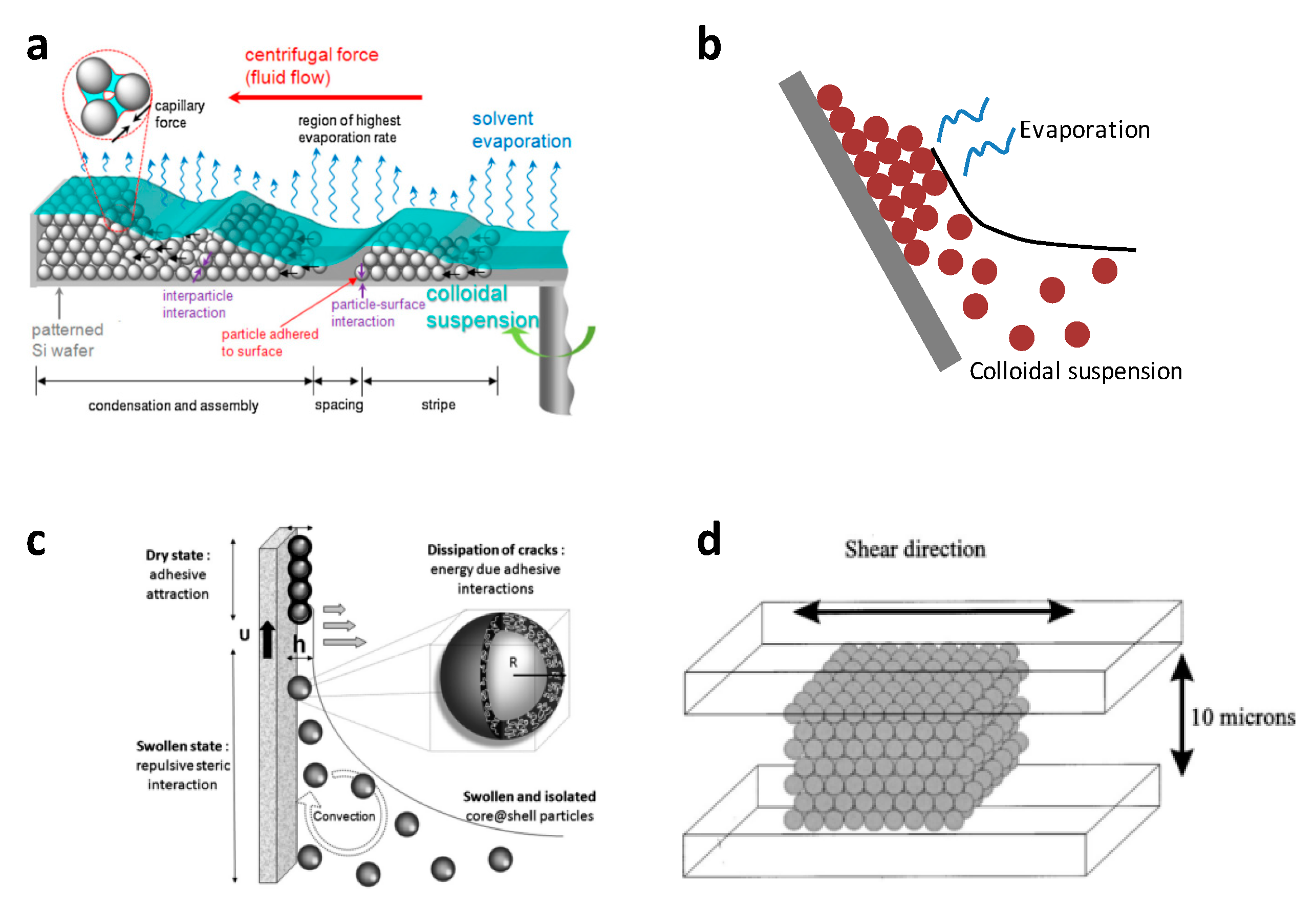
Figure 4.
(a) SEM image of close packed PS monolayer. Scale bar is 2 µm (b) Photographs of PS monolayer on a 1 m² glass substrate, Adapted with permission from Nano Lett. 15, 4591–4598. Copyright (2015) American Chemical Society [48]. (c) PS monolayers of 420 nm spheres. (d) PS monolayers of 337 nm spheres. (e) (2 + 1)D colloidal photonic crystal superlattice formed by stacking colloidal monolayers of 420 nm and 337 nm in ABABAB arrangement [57]. (f) Photograph of a non-closed pack PS monolayer deposited on a four inch wafer. (g) SEM image of a non close-packed PS monolayer [34].
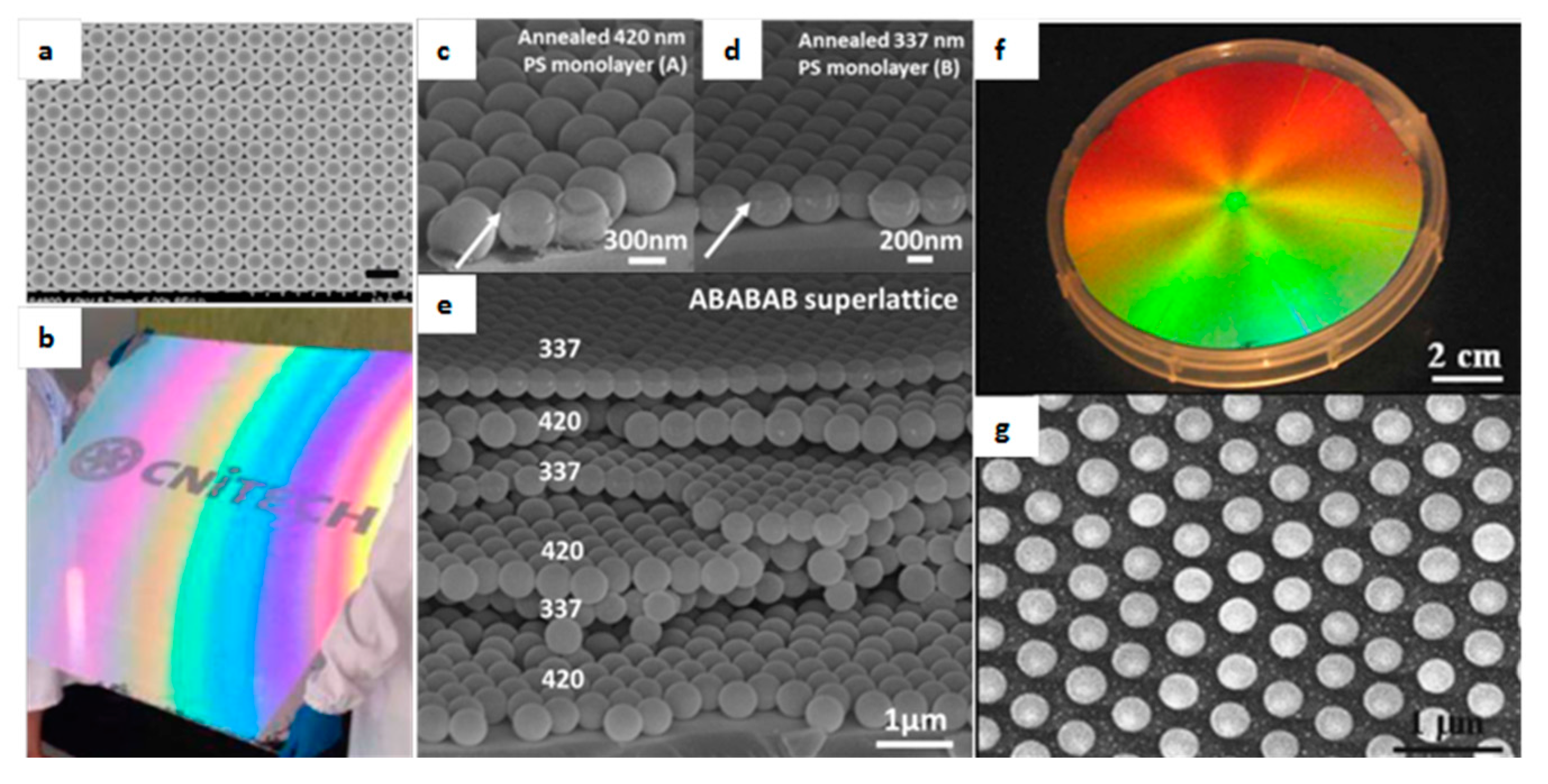
Figure 5.
Making of non-closed packed polystyrene monolayer arrays by oxygen plasma etching under different etching conditions [45]. Scale bars: 200 nm, insets: 500 nm.
Figure 5.
Making of non-closed packed polystyrene monolayer arrays by oxygen plasma etching under different etching conditions [45]. Scale bars: 200 nm, insets: 500 nm.

Figure 6.
(a) Nanoring and (b) nanodot arrays by shadow nanosphere lithography [68].
Figure 6.
(a) Nanoring and (b) nanodot arrays by shadow nanosphere lithography [68].

Figure 7.
(a,b) Nanopillar [65] (adapted with permission from J. Phys. Chem. C 120, 1178–1185. Copyright (2015) American Chemical Society) and (c,d) nanopyramid [64] arrays made by nanosphere lithography (adapted with permission from J. Phys. Chem. C 117, 14778–14786. Copyright (2013) American Chemical Society).

Figure 8.
(a) SEM images of polystyrene opaline structure and (b) titanium dioxide inverse opal structure [116]. Adapted with permission from Langmuir, 24, 1796–1800. Copyright (2008) American Chemical Society.
Figure 8.
(a) SEM images of polystyrene opaline structure and (b) titanium dioxide inverse opal structure [116]. Adapted with permission from Langmuir, 24, 1796–1800. Copyright (2008) American Chemical Society.

Figure 9.
(a–e) Fabrication process for a sik inverse opal. (f) Green and blue silk inverse opals and (g,h) their corresponding SEM images [101].
Figure 9.
(a–e) Fabrication process for a sik inverse opal. (f) Green and blue silk inverse opals and (g,h) their corresponding SEM images [101].

Figure 10.
(a) Monolayer of silica beads on a silicon wafer. Scale bar: 10 µm, inset: 1 µm SEM images: (b) Top view and (c) side view of silicon nanopillars after reactive ion etching. Scale bars are 1 µm (d) Tilted photograph of silicon nanowire radial p-n junction solar cell arrays [75]. Scale bar is 4 cm. Adapted with permission from Nano Lett., 10, 1082–1087. Copyright (2010) American Chemical Society.
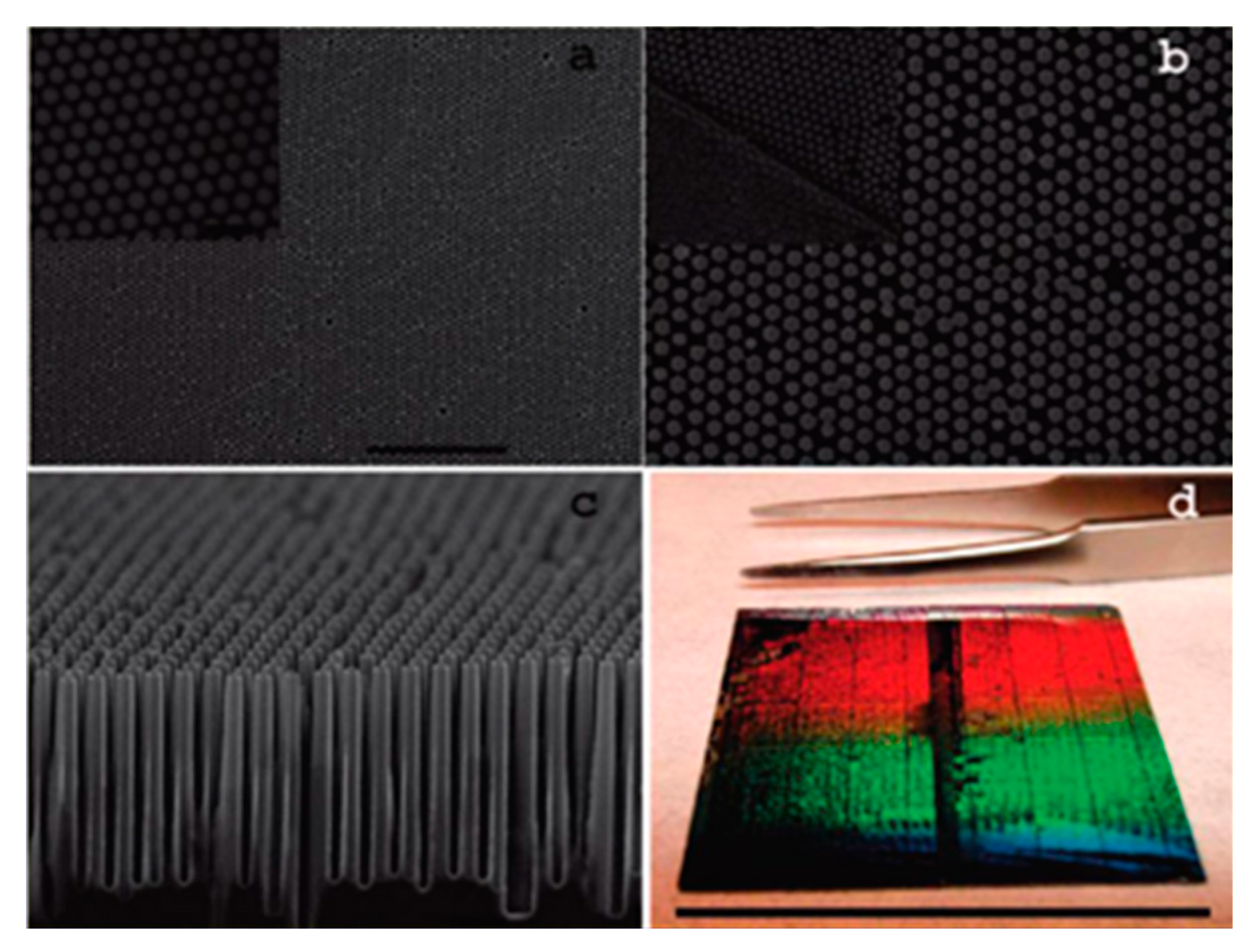
Figure 11.
SEM images of: (a) one; (b) two; and (c) three layers of nanoshells [125]. Scale bars are 300 nm.
Figure 11.
SEM images of: (a) one; (b) two; and (c) three layers of nanoshells [125]. Scale bars are 300 nm.

Figure 12.
(a–c) Cross section SEM images of increasing amounts of gold electrodeposited into a monolayer of polystyrene beads with a diameter D. Scale bars are 300 nm. (d–i) Incidence-angle dependent absorption of gold films containing a monolayer polystyrene beads under (d–f) p- and (g–i) s-polarized incident light. D = 260 nm (d,g); 460 nm (e,h); and 595 nm (f,i) [97].
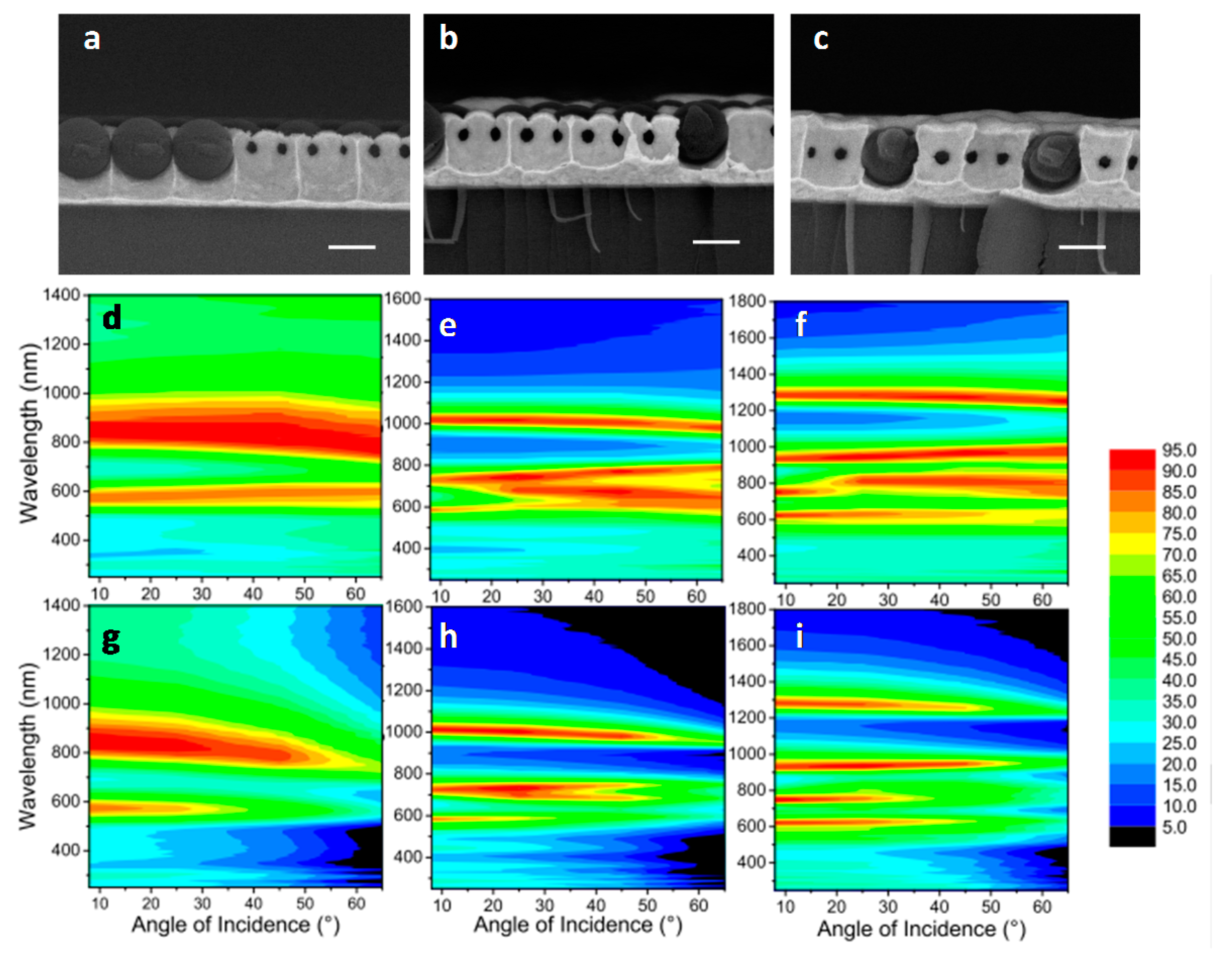
Figure 13.
(a) Schematic illustration of the photovoltaic system with a photonic crystal concentrator. The insert is a SEM image of the photonic crystal concentrator. (b) Photographs of the PC concentrators with different colours [135].
Figure 13.
(a) Schematic illustration of the photovoltaic system with a photonic crystal concentrator. The insert is a SEM image of the photonic crystal concentrator. (b) Photographs of the PC concentrators with different colours [135].

Figure 14.
(a) Photographs of composite Polystyrene/TiO2 films templated with different sizes of PS microspheres and the corresponding TiO2 inverse opal films after calcination. (b) Reflectance spectra of three selected samples from the films shown in the photographs [133].
Figure 14.
(a) Photographs of composite Polystyrene/TiO2 films templated with different sizes of PS microspheres and the corresponding TiO2 inverse opal films after calcination. (b) Reflectance spectra of three selected samples from the films shown in the photographs [133].
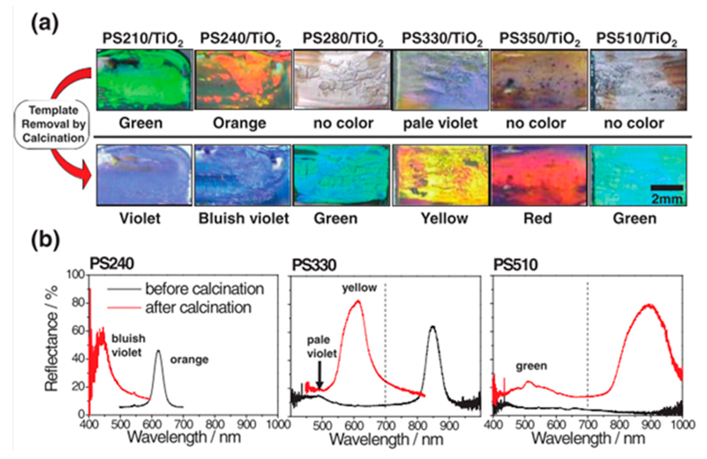
Figure 15.
Transfer of a silicon inverse opal photonic crystal onto dye sensitized ZnO nanowire electrodes [108].
Figure 15.
Transfer of a silicon inverse opal photonic crystal onto dye sensitized ZnO nanowire electrodes [108].
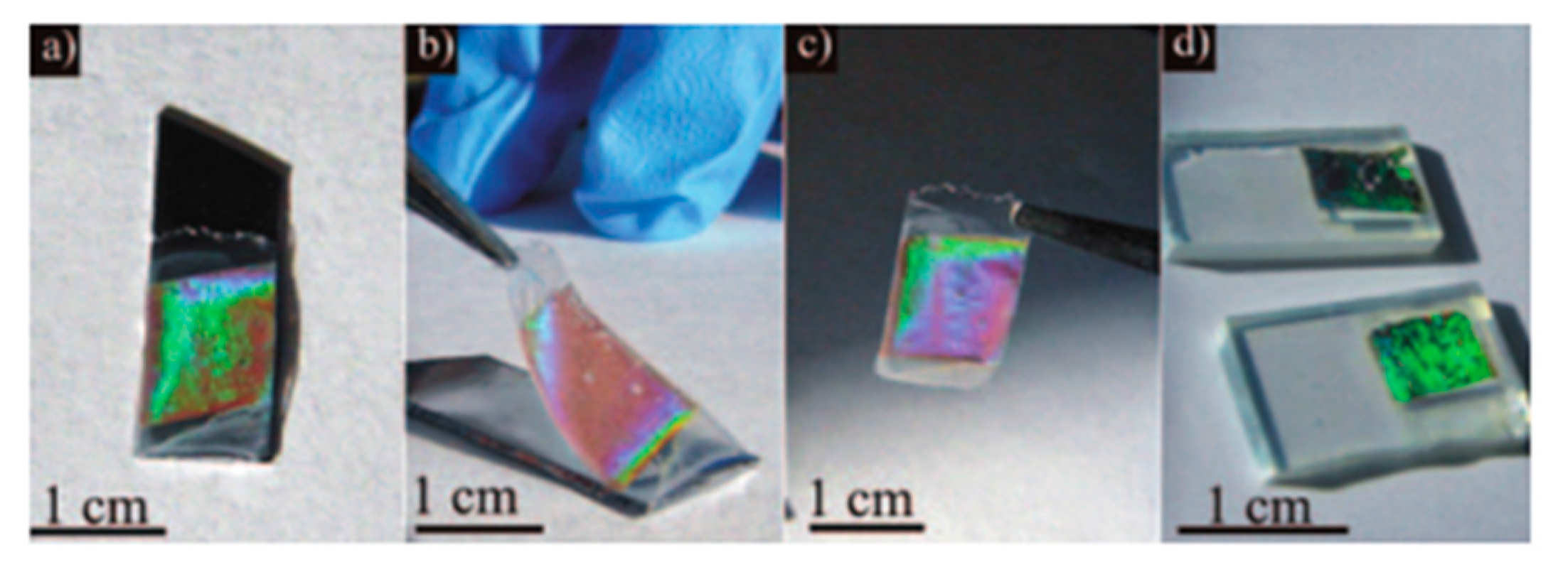
Figure 16.
Schematic of procedure for preparing FTO/nc-TiO2/PC-TiO2 electrodes (a–e); (f) SEM image of the top of the TiO2 inverse opal layer; (g) cell configuration; (h) XRD pattern for TiO2 inverse opal; and (i) cross section SEM image of FTO/nc-TiO2/PC-TiO2 electrodes [136].
Figure 16.
Schematic of procedure for preparing FTO/nc-TiO2/PC-TiO2 electrodes (a–e); (f) SEM image of the top of the TiO2 inverse opal layer; (g) cell configuration; (h) XRD pattern for TiO2 inverse opal; and (i) cross section SEM image of FTO/nc-TiO2/PC-TiO2 electrodes [136].

Figure 17.
Honeycomb-type VLED with a textured cone-shaped deep-pillar surface [139].
Figure 17.
Honeycomb-type VLED with a textured cone-shaped deep-pillar surface [139].
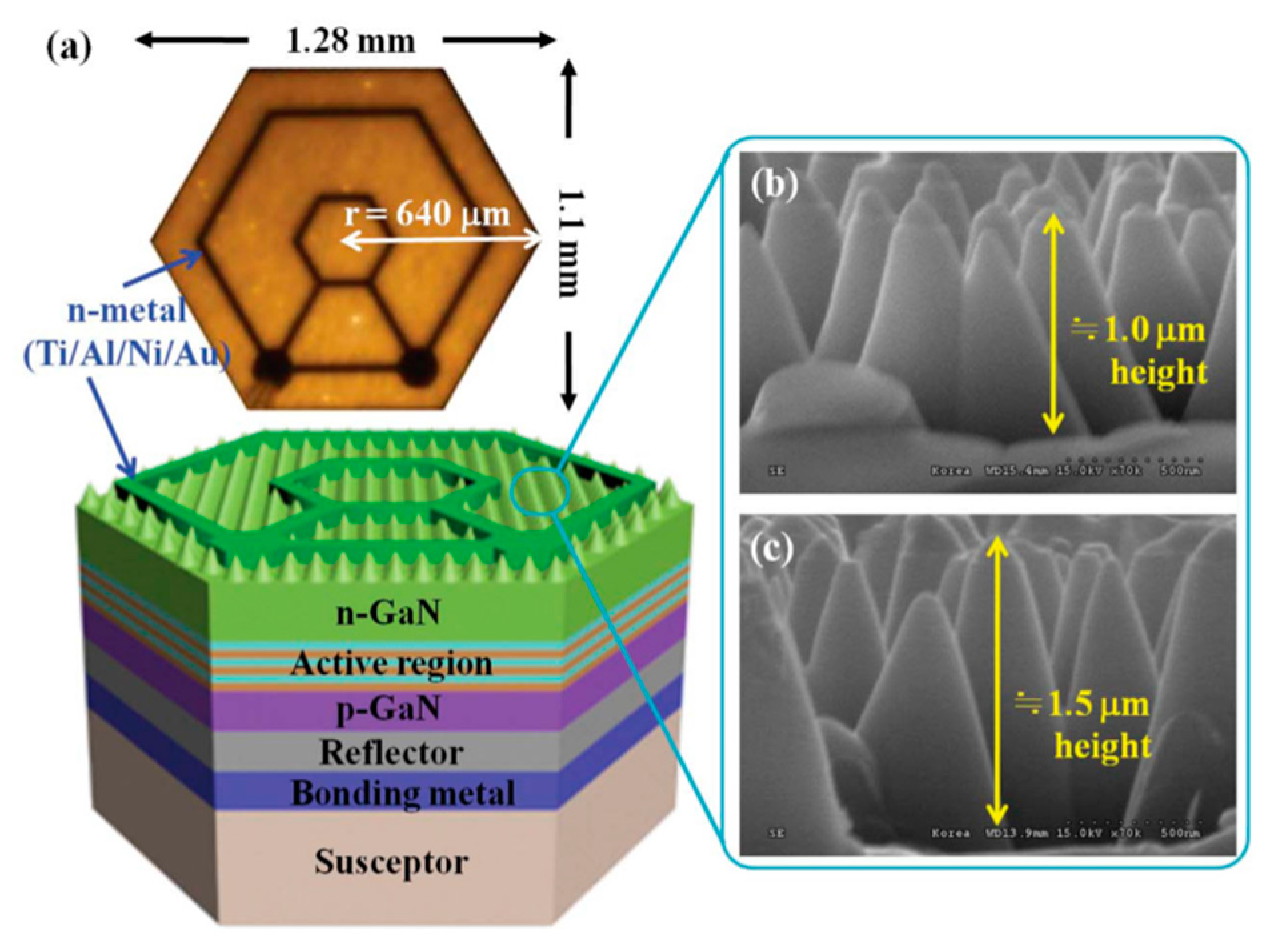
Figure 18.
(a) Schematic illustration and (b) SEM of the structure of the LED with the embedded photonic crystal layer [140].
Figure 18.
(a) Schematic illustration and (b) SEM of the structure of the LED with the embedded photonic crystal layer [140].

Figure 19.
Diffraction wavelength versus sodium dodecyl sulphate (SDS) concentration. Inset: photographs taken close to the Littrow configuration at a 28° angle between source and camera to the 2D array normal [148]. Adapted with permission from Anal. Chem. 84, 6416–6420. Copyright (2012) American Chemical Society.
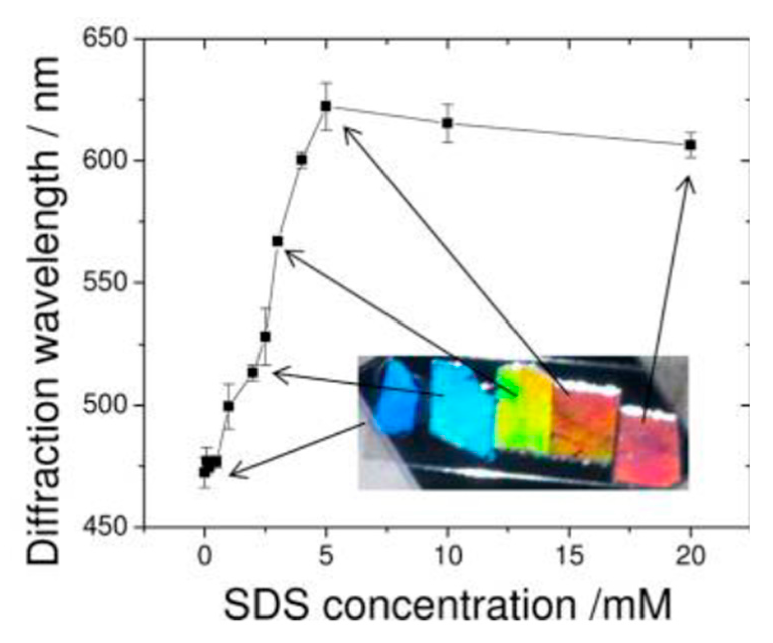
Figure 20.
Reflection spectra of the various non-modified (solid lines) and porphyrin-modified (dotted lines) colloidal crystals [149]. Adapted with permission from ACS Appl. Mater. Interfaces, 4, 6752–6757. Copyright (2012) American Chemical Society.
Figure 20.
Reflection spectra of the various non-modified (solid lines) and porphyrin-modified (dotted lines) colloidal crystals [149]. Adapted with permission from ACS Appl. Mater. Interfaces, 4, 6752–6757. Copyright (2012) American Chemical Society.
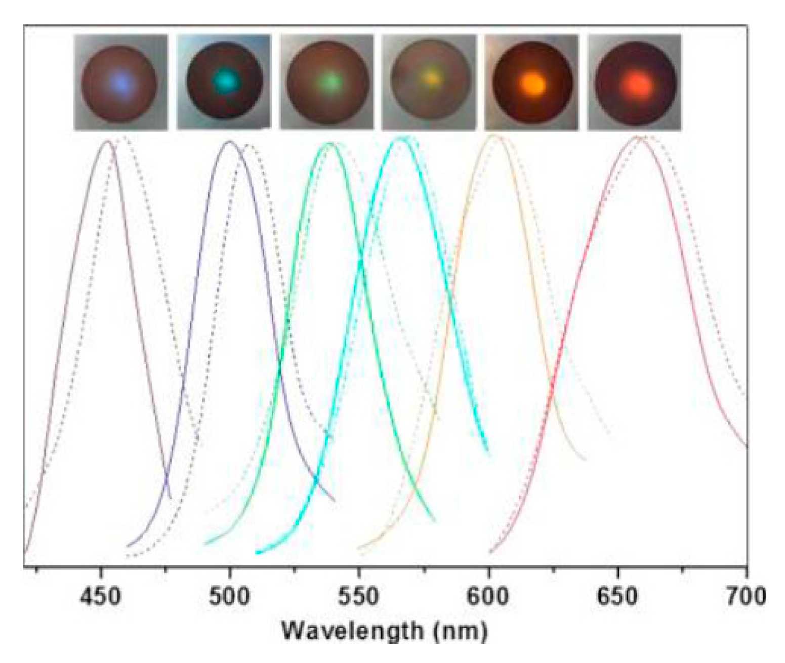
Figure 21.
(a) pH-dependent color change and respective reflectance spectra of hydrogel pH sensors between pH of 1.26 and 6.99. A series of spectra were measured during pH increase (solid curves) and during pH decrease (dashed curves). (b) Plot of λmax change during pH increase and decrease showing a weak hysteresis [152].


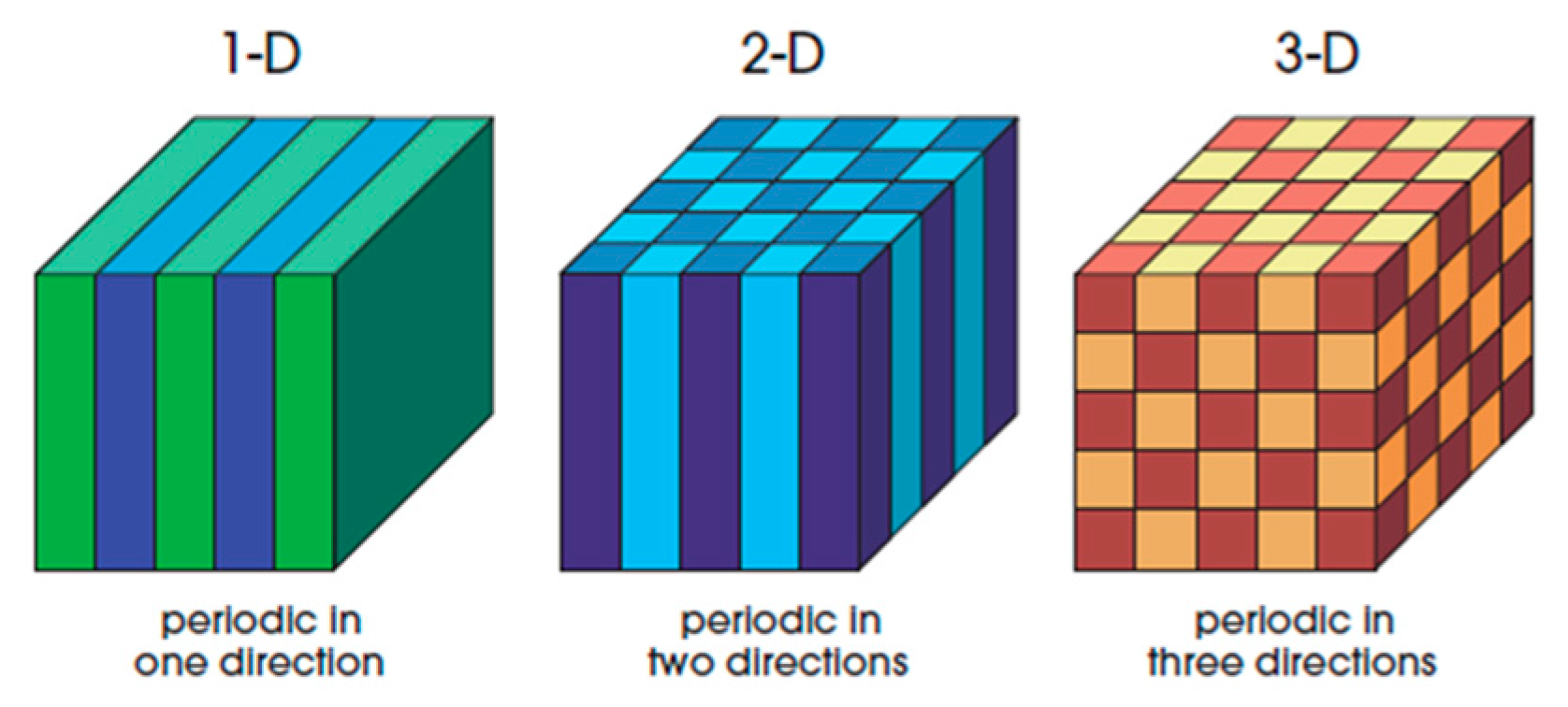
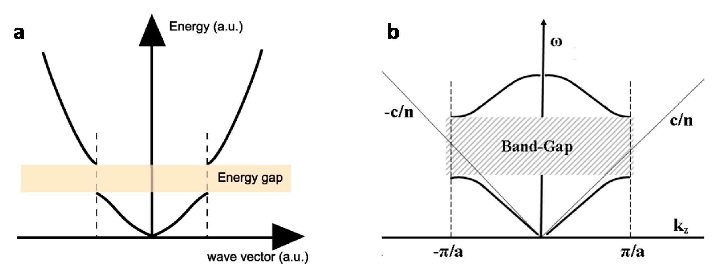
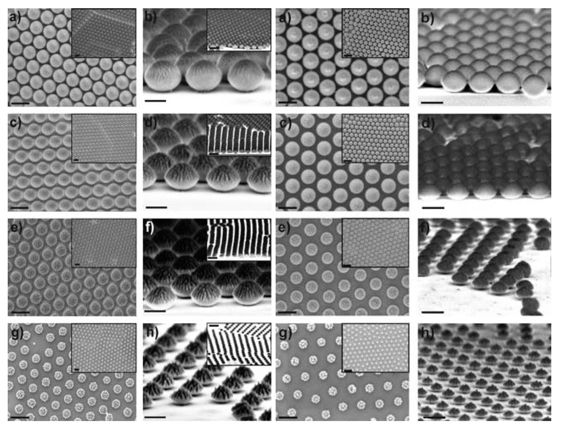
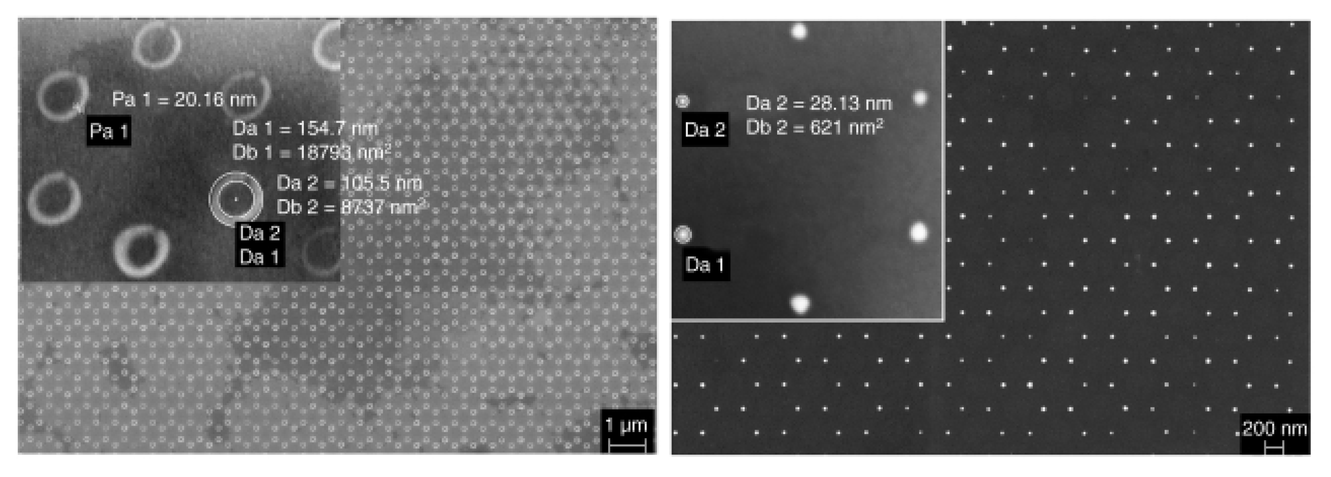
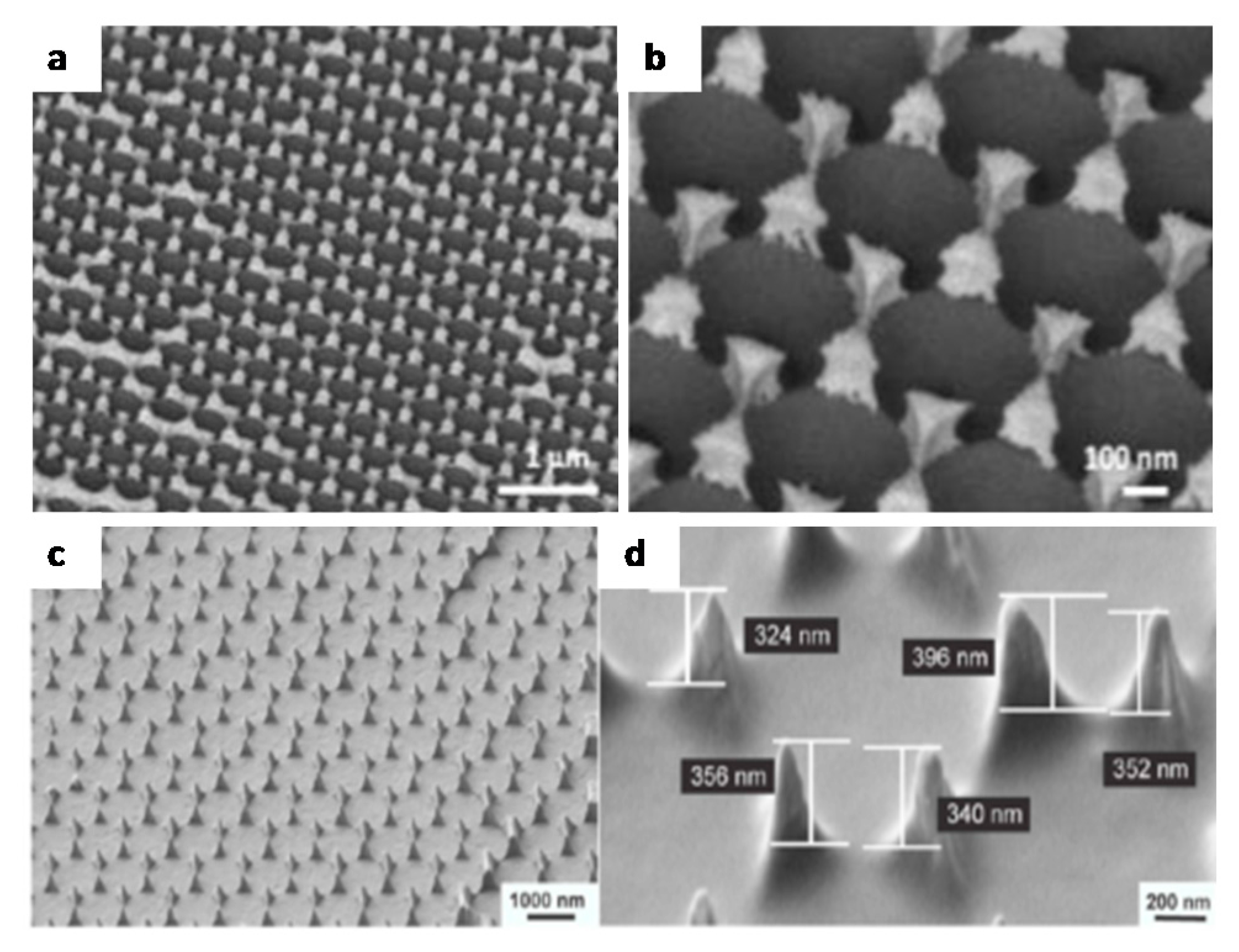
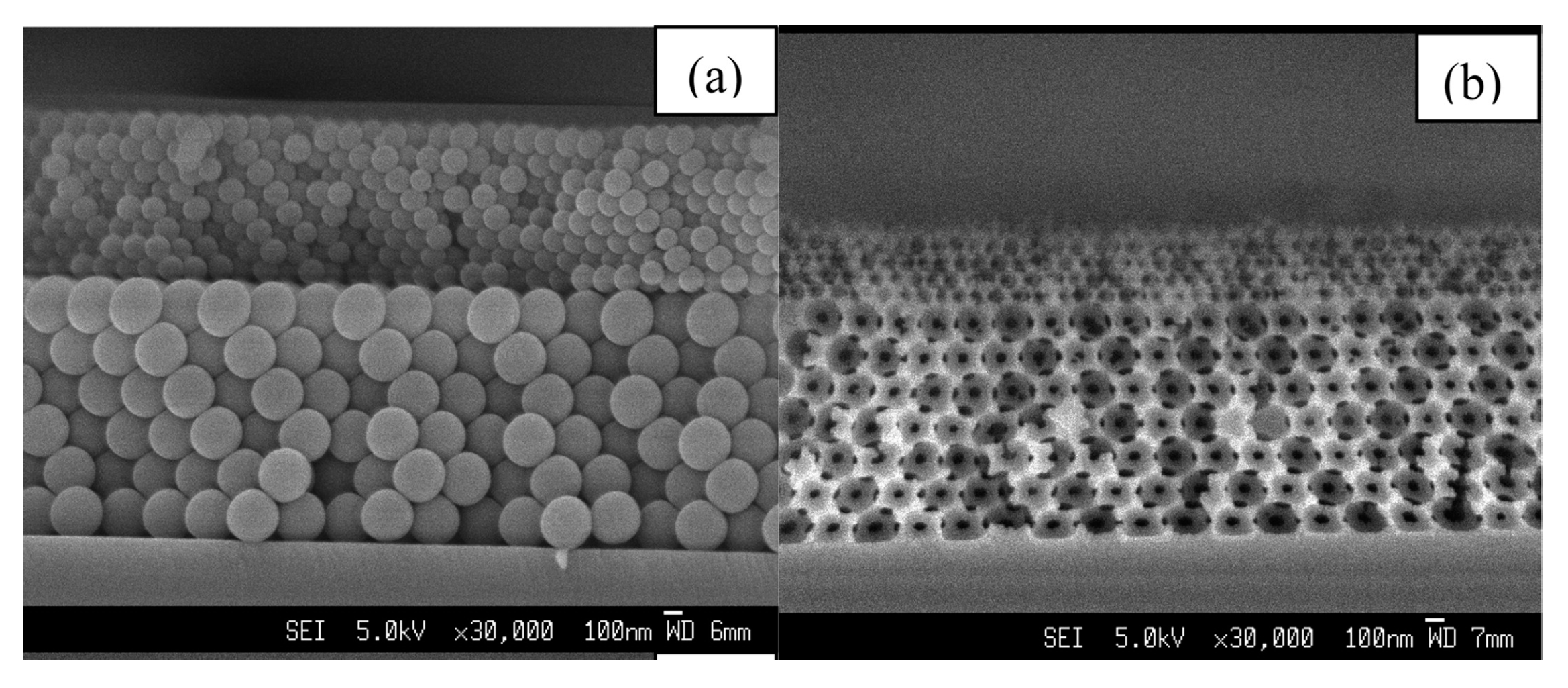
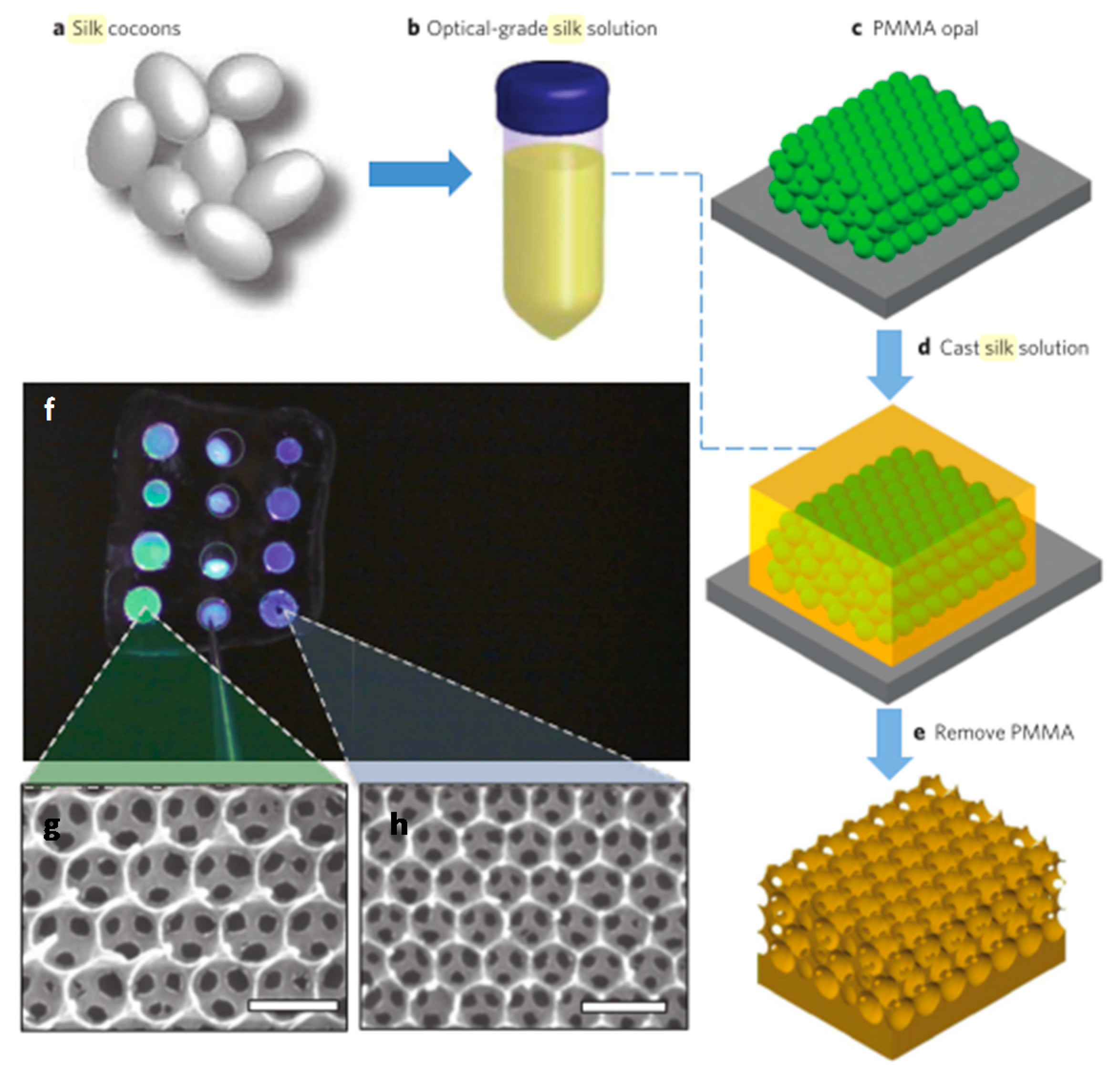
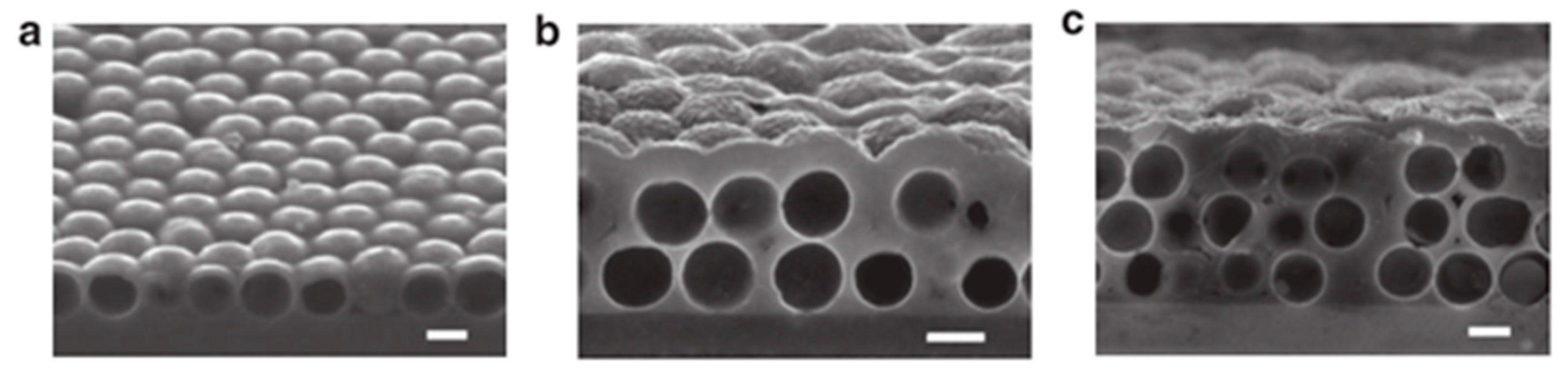
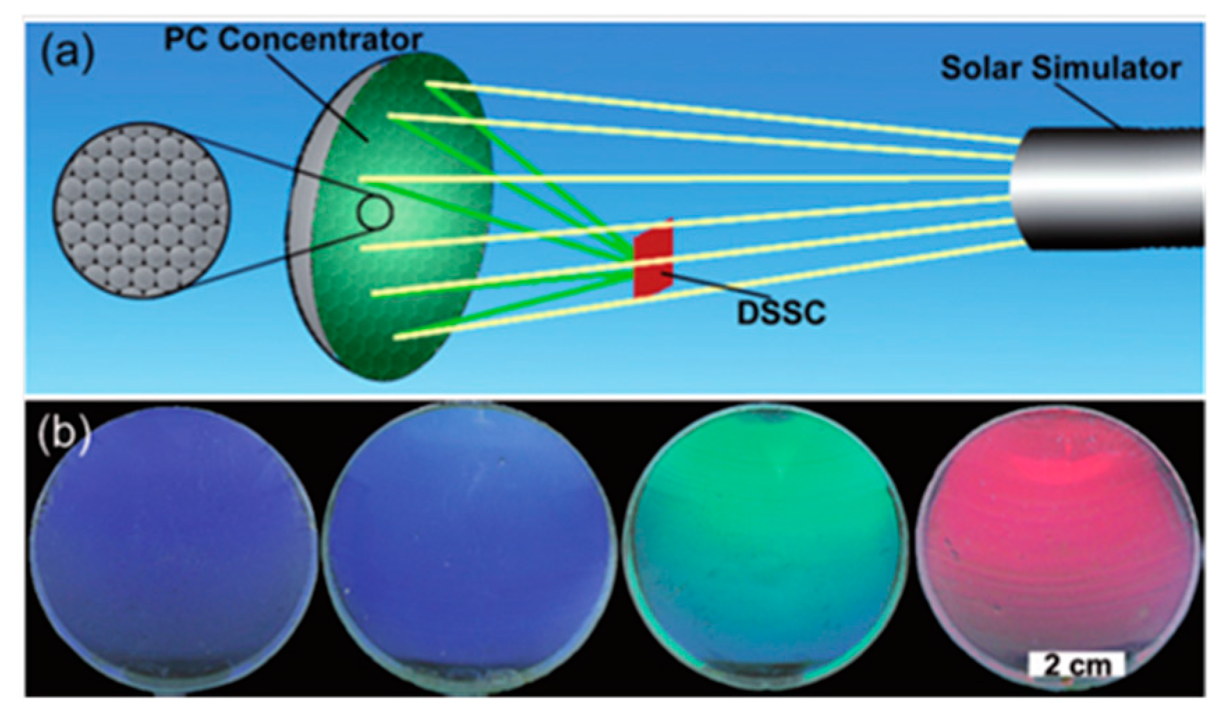
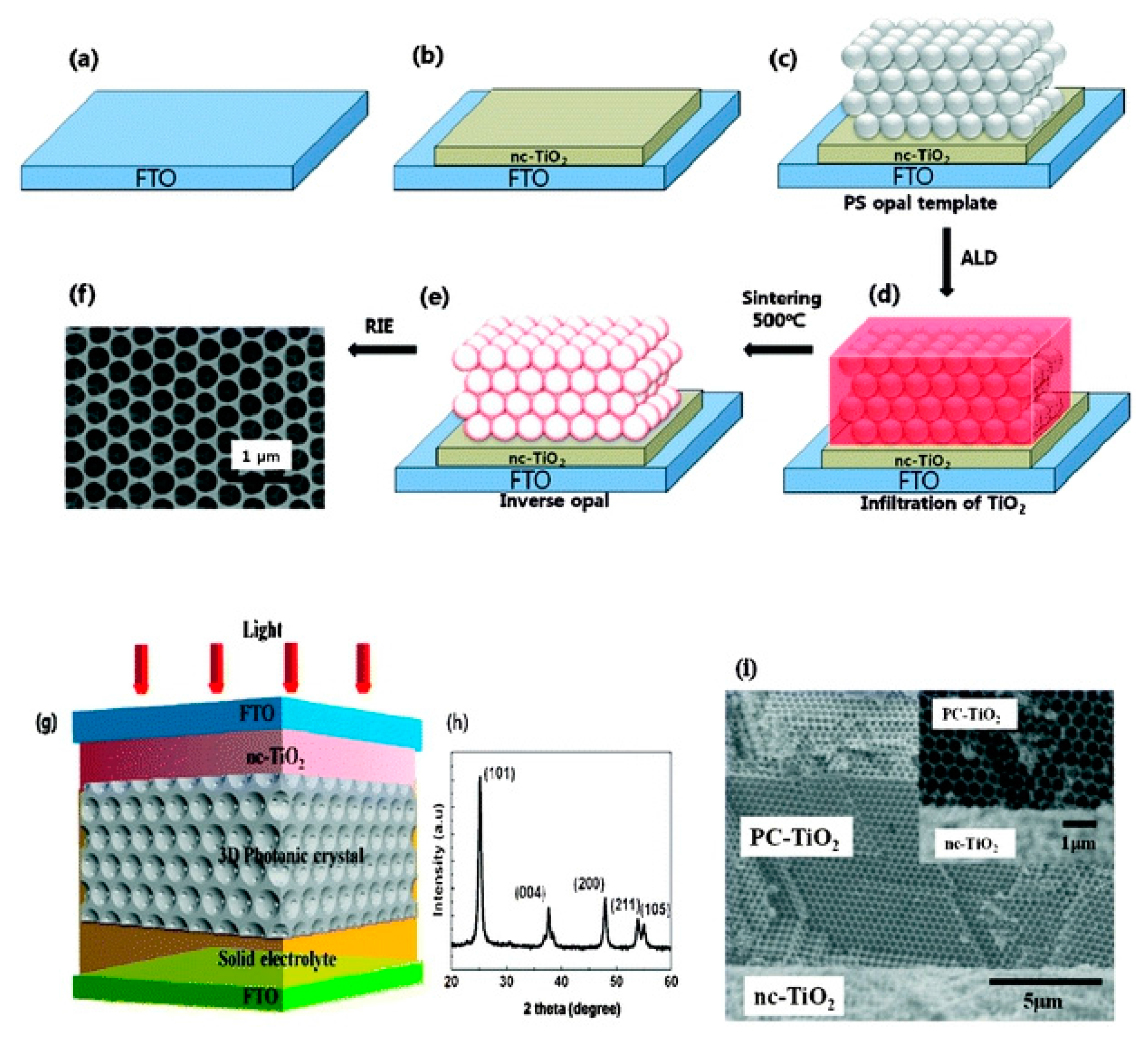
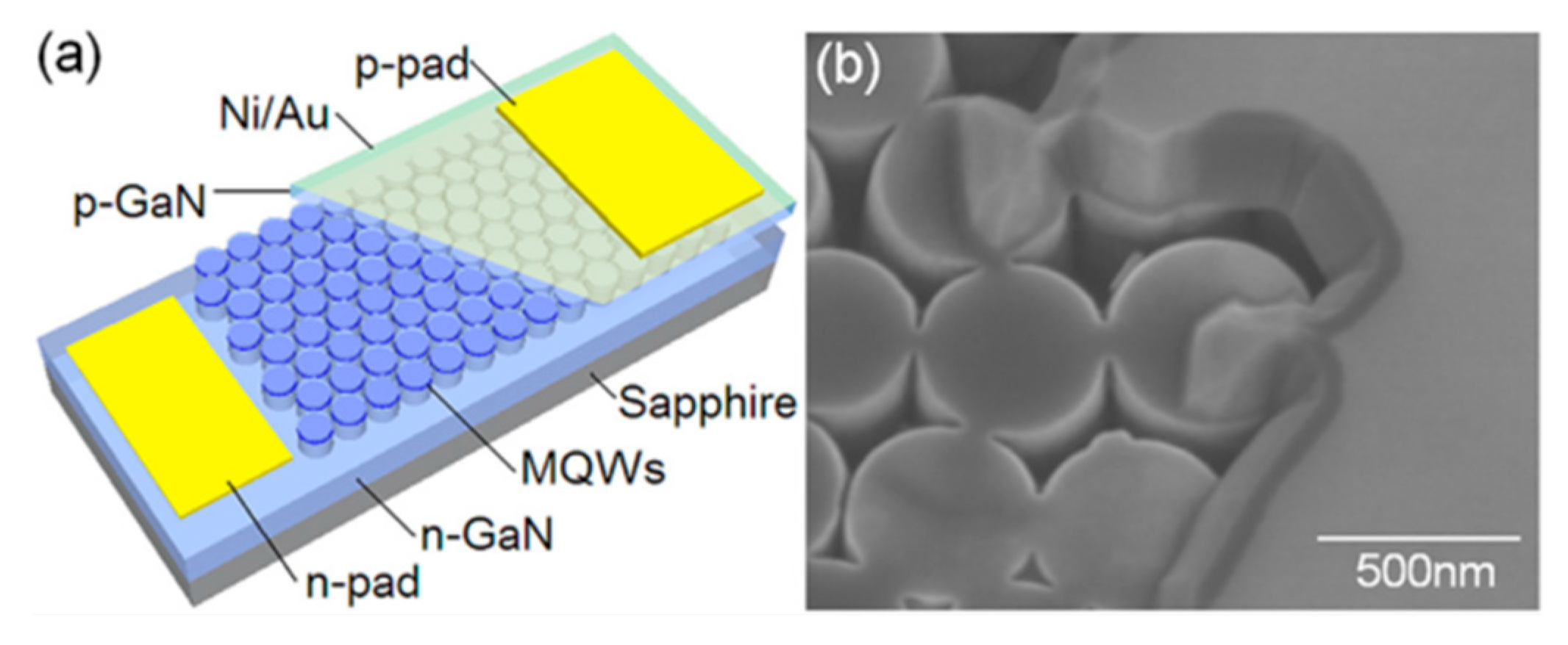
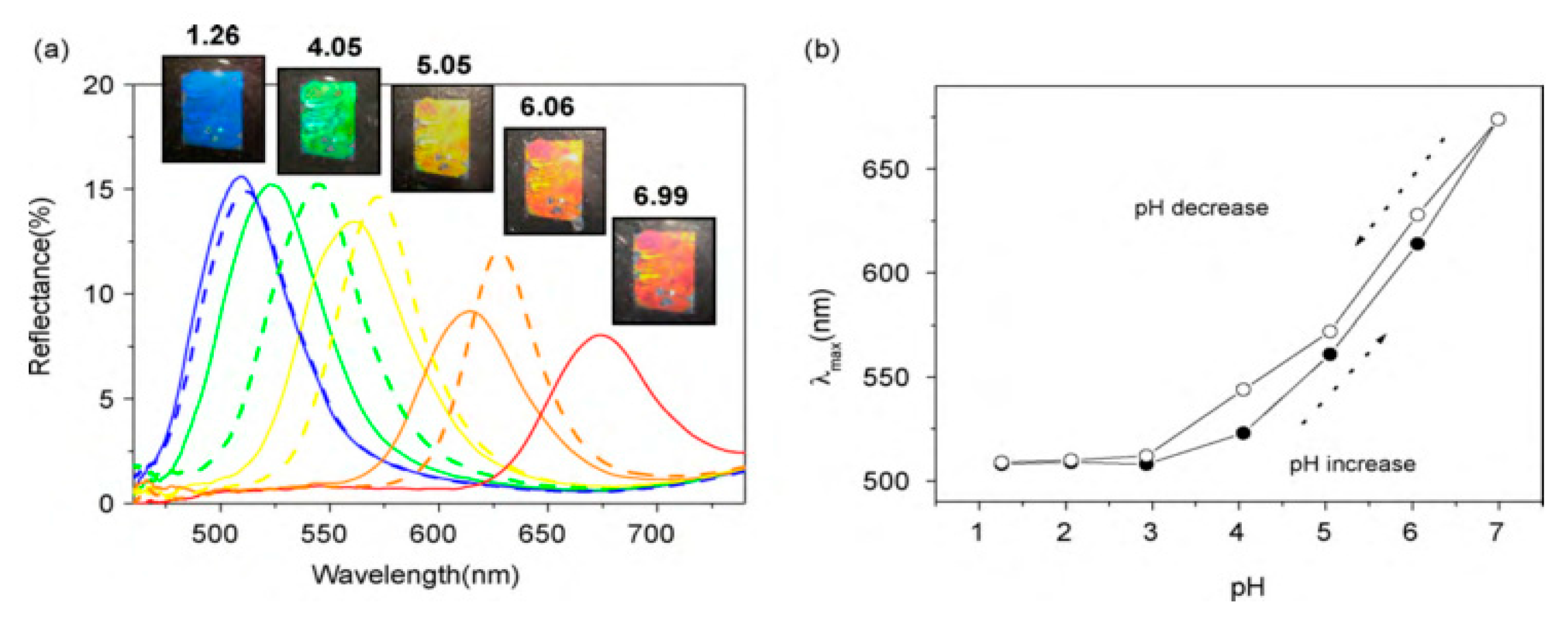
| Method | Remarks |
|---|---|
| Drop casting (Sedimentation) [24,25] | Simple but slow process. Patches of colloidal crystals formed. Difficult to control exact conditions |
| Vertical deposition [26,27,28] | Requires very good control of evaporation conditions (i.e., temperature and humidity) for a good deposition. Slow process (days). Very good quality of colloidal crystals formed under the proper conditions Gradient in the thickness of colloidal crystal formed |
| Centrifugation [29] | Simple and fast process. Generally big bulky colloidal crystals formed. |
| Spin-coating [30,31,32,33,34,35] | Simple and fast process. Monolayer formation possible. Patches of small coating area of monolayers. |
| Dip-coating [36,37,38] | Can control thickness of layers by the speed of withdrawal. Gradient in layer thickness. [27] |
| Shear ordering [39] | Requires very good control of process parameters Slow process Makes thin films |
| Langmuir-Blodgett [40,41,42,43,44] | Monolayer compressed on water surface by mobile arms. Short range order of closed packed regions within the monolayer. Monolayer transfer onto substrate can be repeated to deposit multilayers exactly as desired. Takes time for preparation of equipment and spreading of particles. |
| Direct assembly on water surface [45,46,47,48] | Simple and fast process. Good two-dimensional closed pack array on water surface. One monolayer at a time can be transferred. Can be repeated to deposit multilayers exactly as desired. |
| Magnetic self-assembly [49,50,51] | Requires highly-charged monodisperse magnetic colloidal particles Self-assembly occurs inside liquid medium Can be controlled by external magnetic field |
© 2016 by the authors; licensee MDPI, Basel, Switzerland. This article is an open access article distributed under the terms and conditions of the Creative Commons Attribution (CC-BY) license (http://creativecommons.org/licenses/by/4.0/).
Share and Cite
MDPI and ACS Style
Zheng, H.; Ravaine, S. Bottom-Up Assembly and Applications of Photonic Materials. Crystals 2016, 6, 54. https://doi.org/10.3390/cryst6050054
AMA Style
Zheng H, Ravaine S. Bottom-Up Assembly and Applications of Photonic Materials. Crystals. 2016; 6(5):54. https://doi.org/10.3390/cryst6050054
Chicago/Turabian StyleZheng, Hanbin, and Serge Ravaine. 2016. "Bottom-Up Assembly and Applications of Photonic Materials" Crystals 6, no. 5: 54. https://doi.org/10.3390/cryst6050054
Note that from the first issue of 2016, this journal uses article numbers instead of page numbers. See further details here.