Review

Topological Insulator Film Growth by Molecular Beam Epitaxy: A Review

Department of Materials Science and Engineering, University of Delaware, 127 The Green Room 201, Newark, DE 19716, USA
*
Author to whom correspondence should be addressed.
Crystals 2016, 6(11), 154; https://doi.org/10.3390/cryst6110154
Submission received: 4 October 2016 / Revised: 16 November 2016 / Accepted: 18 November 2016 / Published: 23 November 2016

Abstract

:
In this article, we will review recent progress in the growth of topological insulator (TI) thin films by molecular beam epitaxy (MBE). The materials we focus on are the V2-VI3 family of TIs. These materials are ideally bulk insulating with surface states housing Dirac excitations which are spin-momentum locked. These surface states are interesting for fundamental physics studies (such as the search for Majorana fermions) as well as applications in spintronics and other fields. However, the majority of TI films and bulk crystals exhibit significant bulk conductivity, which obscures these states. In addition, many TI films have a high defect density. This review will discuss progress in reducing the bulk conductivity while increasing the crystal quality. We will describe in detail how growth parameters, substrate choice, and growth technique influence the resulting TI film properties for binary and ternary TIs. We then give an overview of progress in the growth of TI heterostructures. We close by discussing the bright future for TI film growth by MBE.

Graphical Abstract

1. Introduction

Topological insulators (TIs) are materials with a band structure comprising a bulk bandgap crossed by surface states with linear dispersion [1,2,3,4]. These surface states exhibit spin-momentum locking, implying that the spin of a particle in these surface states is determined by its momentum [5]. This leads to a prohibition on backscattering and a reduction in scattering at other angles from nonmagnetic impurities, vacancies, and other defects, since a change in momentum requires a change in spin. However, surface electrons may still exhibit phonon scattering (though the strength of this interaction is not well-known) as well as interactions with bulk states, if available [6,7]. The linear dispersion of these states leads to essentially massless particles with a large Fermi velocity. If the Fermi energy of the TI can be placed within the bulk bandgap, all conduction will ideally take place on the surfaces, enabling the creation of devices which exploit the unusual properties of these surfaces. Applications of TIs include a platform for housing Majorana fermions, the creation of a large variety of spin devices, topological quantum computation, and others [8,9,10,11,12].
TIs were first predicted theoretically in two-dimensional HgTe/CdTe quantum wells [13,14]. The realization that three-dimensional TIs could exist followed soon after [15,16,17]. Three-dimensional TIs were first experimentally demonstrated by imaging the band structure of the alloy BixSb1−x using angle resolved photoemission spectroscopy (ARPES) [18,19], closely followed by measurements of bulk crystals of Bi2Se3, Bi2Te3, and Sb2Te3 [1,2,3,4]. This confirmation of the existence of TIs led to an explosion of research in this field, both theoretically and experimentally. For a review of the history of the field, the reader is referred to [20]. As mentioned above, TI materials can be grown in bulk crystal form, from which thin films can be exfoliated. Additionally, thin films can be grown directly on a variety of substrates using chemical vapor deposition (CVD) techniques as well as molecular beam epitaxy (MBE), which will be the focus of this review [21]. MBE-grown films have a number of advantages over exfoliated films, including large area growth and the ability to controllably dope the materials, resulting in recent observations of the quantum anomalous Hall effect [22,23,24,25,26,27]. Unfortunately, both bulk crystals and thin films tend to exhibit significant conductivity from non-topological electrons, either from bulk states and/or from surface accumulation layers [28,29]. This is a particular problem for electrical measurements and applications, as the electrical signal from the non-topological electrons can overwhelm the signal from the surface states even in very thin films. Additionally, TIs frequently exhibit aging effects in which the film properties change over time, even in vacuum. In this review, we will discuss recent progress in the growth of TIs by MBE. First we will show the crystal structure of the V2VI3 compounds of interest, followed by a discussion of van der Waals epitaxy and substrate choice. We will then discuss each family of compounds in order, including binary and ternary films. We will end with a discussion of heterostructures, including TI structures and combined TI/band insulator (BI) materials.

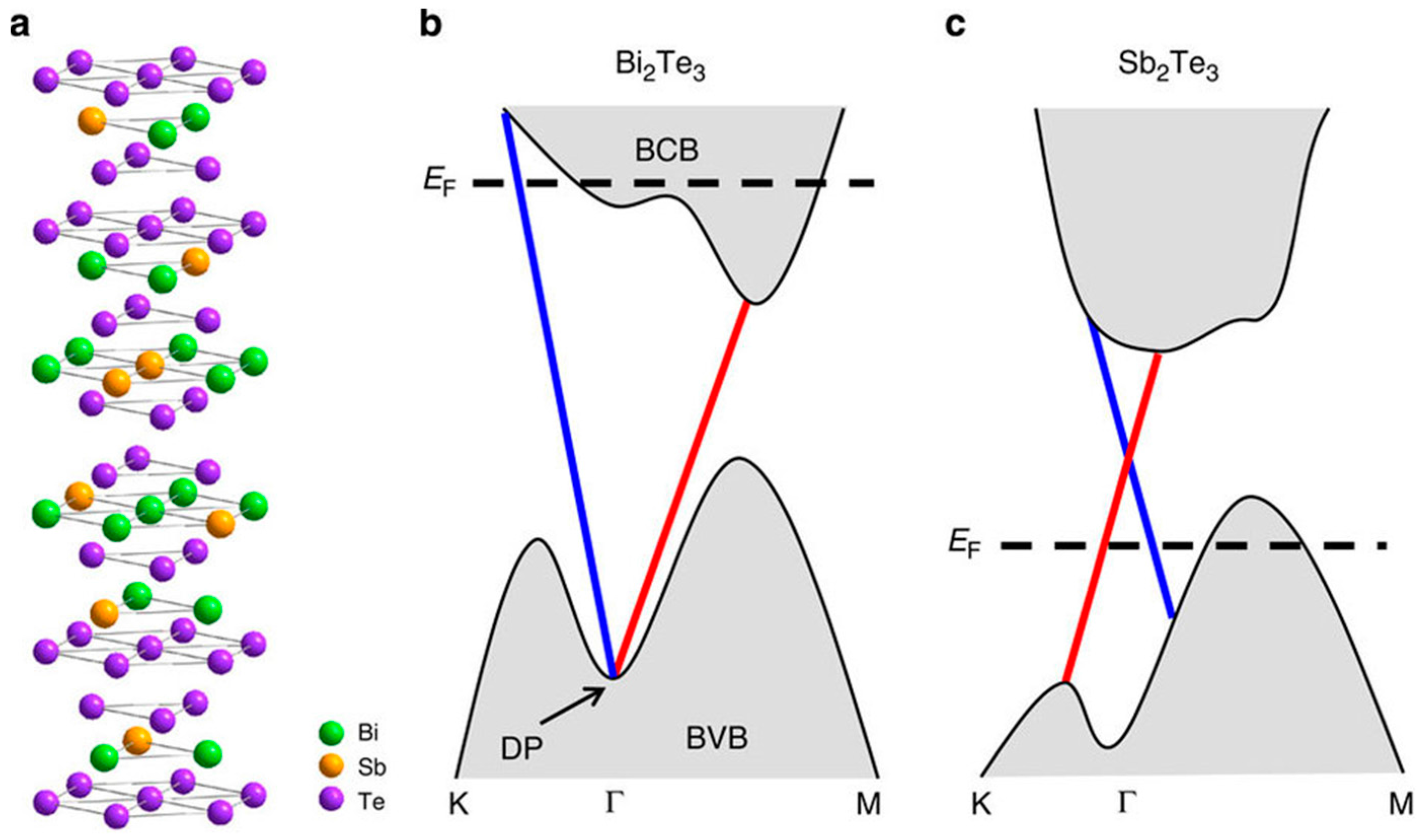
1.1. Crystal Structure

Topological insulators are comprised of heavy elements with strong spin-orbit coupling. The strong spin-orbit coupling causes the valence band states to be pushed higher in energy than the conduction band states, leading to a band renormalization. As a first approximation, one can now imagine that the bottom of the conduction band near the Γ point is comprised of states with the symmetry of the valence band, and the top of the valence band is comprised of states with the symmetry of the conduction band. This is an inverted band structure. At the surfaces of the TI, this inverted band structure interfaces with a normal band structure. Boundary conditions require that the valence band states in the TI which have conduction band character connect with the conduction band in the normal material, and vice versa. This leads to the surface states which are of interest in TI materials. These surface states are depicted in the calculated Bi2Se3 band structure shown in Figure 1. To first order, the spin-momentum locking of the surface electrons comes from the strong spin-orbit coupling of the heavy elements that comprise the material. This explanation of TI behavior is quite basic and ignores many complications, but it is sufficient to see that strong spin-orbit coupling is required for the formation of a strong TI. For a more thorough treatment of the theory behind the TI band structure, the reader is referred to [12]. The prototypical TI materials are Bi2Se3, Bi2Te3, Sb2Te3, and their alloys. These materials have been known for many years as good thermoelectrics and were grown by MBE for that purpose long before they were investigated for their topological properties.
The crystal structure of Bi2Se3 is shown in Figure 2. It is a tetradymite structure with space group D 3 d 5 ( R 3 ¯ m ) . The other TI materials discussed in this review have the same structure. The basic building block of the chalcogenide TIs is the quintuple layer (QL); two QLs are shown in Figure 2(a). Each QL is ~1 nm, though precise values vary from compound to compound. The stacking structure within a QL is Se1-Bi-Se2-Bi-Se1. Each QL is chemically stable, leading to a van der Waals gap between QLs. This weak interlayer bonding allows TI layers to easily be exfoliated from bulk crystals. It also allows MBE growth to take place on a wide variety of substrates, since the film is only weakly bound to the substrate. This type of growth is traditionally called van der Waals epitaxy [30,31]. However, there is evidence that choosing lattice-matched substrates can significantly improve the film growth, as will be discussed in detail in this article.

1.2. Substrate Choice
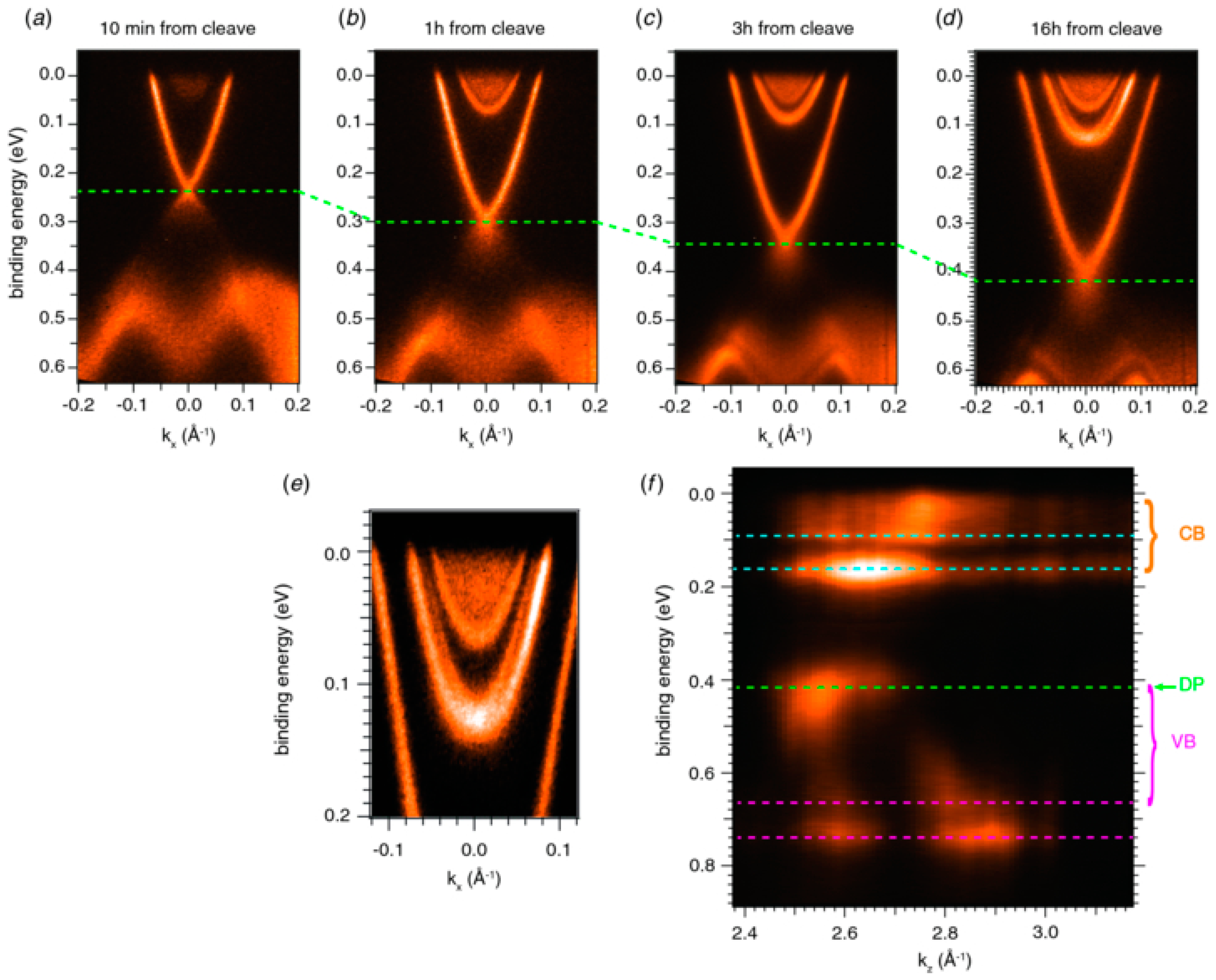
The most common substrate used for MBE growth of TIs is c-plane sapphire (Al2O3) which has the same in-plane structure as the TIs. Almost all Bi2Se3 growth takes places on sapphire [33], though other materials are frequently grown on other substrates, as described in detail in Section 2. Sapphire has a variety of advantages, including its low cost, easy availability, high surface quality, and general chemically inert behavior. However, there is some evidence that the large lattice mismatch between sapphire and TIs (almost 15% for Bi2Se3) can lead to a variety of structural defects, including mosaicity-tilt, mosaicity-twist, antiphase domain boundaries (APBs), and twin defects [34,35,36,37]. In Figure 3, we present a plot of lattice constant for some of the common TIs and the available substrates.
The difficulty in using many of the more closely lattice-matched substrates is the presence of dangling bonds and surface oxide layers. InP (111), for example, is closely lattice-matched to Bi2Se3. However, InP has a surface oxide that is normally thermally desorbed at a relatively high temperature. This high temperature leads to phosphorous outgassing from the sample, which must be compensated. In a traditional III/V chamber, a phosphorous flux is easy to supply, but this becomes much more difficult in a chalcogenide-only chamber. Some success has been obtained by supplying the chalcogenide atom in excess when desorbing surface oxides from III/V and other substrates [38]. In addition to surface oxides, a large fraction of the available substrates have surface dangling bonds which must be satisfied. Again, there has been some success in passivating these surfaces by supplying a chalcogenide overpressure [39,40,41] or by depositing a monolayer of bismuth [42]. These growth challenges as well as the relatively high cost of many lattice-matched substrates is why most growth continues on sapphire.
There have been recent promising reports of Bi2Se3 grown using buffer layers or virtual substrates. In2Se3 is a trivial band insulator with the same layered crystal structure and similar lattice constant to the TIs discussed in this article. Thus, theoretically, using In2Se3 as a buffer layer could enhance the crystal quality of Bi2Se3 films. Systematic optimization of MBE growth parameters of In2Se3 on Si(111) substrate was reported by Rathi et al. [43]. The authors concluded that the In2Se3 layers that are most suitable for Bi2Se3 growth resulted from a three-step growth sequence: Se passivation of the Si substrate at 100 °C, In2Se3 codeposition with a temperature ramp from 100 °C to 400 °C, followed by Se anneal at 400 °C. They also successfully grew Bi2Se3 on top of In2Se3 with a sharp interface. Koirala et al. [44] reported that using (InxBi1−x)2Se3 as a buffer layer between Bi2Se3 and sapphire substrate reduced defects in the Bi2Se3 crystal and caused an order of magnitude enhancement in the mobility over films grown without the buffer layer. Further discussion of substrate choice for different material systems will be described within each topic below, but these results indicate that substrate choice and preparation is crucial for high-quality growth of TIs.

1.3. Aging Effects

One of the other challenges when working with TIs is the effect of aging. ARPES measurements performed on newly grown thin films and freshly cleaved bulk crystals for Bi2Se3 and Bi2Te3 frequently show a surface Fermi level within the bulk bandgap, above the Dirac point. Over the course of a few days in vacuum or a few hours in air, the Fermi level rises into the conduction band [45,46,47,48,49,50,51]. The case of Sb2Te3 is somewhat different, with the Fermi level of new films and freshly cleaved crystals residing below the Dirac point, frequently in the valence band. There are few reports of how the band structure of these material changes over time, but the existing data indicate a relatively stable Fermi energy despite the large background doping, in contrast to the bismuth-based materials [4,52,53,54]. The exact mechanism behind the change in Fermi level in Bi2Se3 and Bi2Te3 is not well known, but it is thought to be due to a combination of selenium/tellurium outgassing from the film, oxygen diffusing into vacancies, and adsorption of other gasses on the film surface. This results in bands which normally bend downward at the surface, leading to a surface accumulation layer with the Fermi level in the conduction band and a trivial two-dimensional electron gas (2DEG) at the surface, as shown in Figure 4. Although this aging effect makes it more difficult to observe the effects of the surface states due to the increase in the trivial carrier density, the surface states still exist within the film.

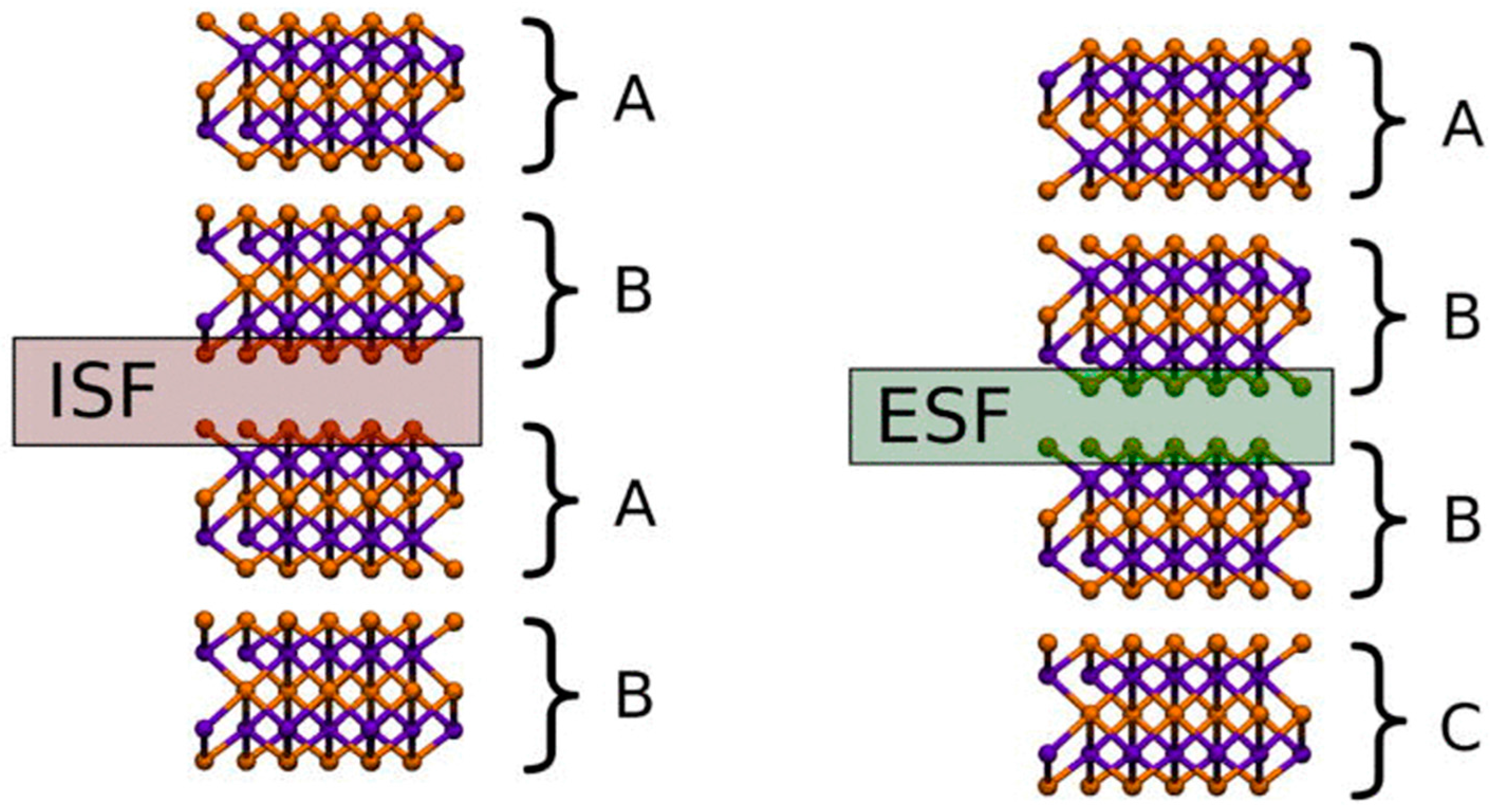
1.4. TI Film Structural Quality

As mentioned previously, TI films can suffer from a variety of structural defects, including mosaicity-tilt, mosaicity-twist, antiphase domain boundaries (APBs), stacking faults, and twin defects [34,35,36,37]. Details about these defects and strategies to reduce them will be discussed for each material class separately in Section 2, but we will give an overview of the subject here. It should be emphasized that the topological surface state is robust and exists even in defective films. For electrical devices, the most important metrics of film quality are carrier density and mobility—high quality TI films should have a low trivial carrier density and a high mobility for the electrons in the surface states. Trivial carrier density tends to be determined by point defects, including vacancies and antisite defects, as well as surface band bending, as discussed in detail in Section 2. Mobility is determined both by point defects as well as by the line and planar defects as listed above.
Due to the in-plane three-fold symmetry of the crystal (shown in Figure 2b), TI materials are highly susceptible to structural defects. There are three possible orientations for a TI domain, A, B, and C. A perfect stacking sequence in the growth direction would be ABCABCABC, with each QL rotated 120° from the previous QL. A stacking fault occurs when a single QL is removed, leading to a sequence of e.g., ABABCABC, or when a single QL is added, leading to a sequence of e.g., ABBCABCABC, as shown schematically in Figure 5. Stacking faults may have profound effects on the electrical properties of the film, including forming topologically protected states along the fault or shifting the Dirac point with respect to the pristine band structure [55]. These types of defects are generally difficult to prevent.
Twin defects occur when two domains with different stacking sequences meet. Twin defects occur over a much larger area than stacking faults. A change in stacking in the vertical direction leads to a lamellar twin, while a change in stacking in the plane leads to a rotational twin. Rotational twin defects appear as oppositely-oriented triangular domains in atomic force microscopy (AFM) scans (see Section 2.1.3; both types of twin defects can be viewed using transmission electron microscopy (TEM) [34,42,56]. In general, a higher structural quality film will show fewer, larger triangular domains, which correlates with a higher mobility (see Table 1). The domain size generally becomes larger when the film is grown on a lattice-matched substrate or through optimizing the substrate temperature, growth rate, and flux ratios [34,37,42,57,58]. Details regarding growth techniques to reduce twinning are given in Section 2.
Antiphase domains occur due the difference in unit cell height between the substrate and the TI film. The substrate is comprised of large, flat terraces with step heights equal to the substrate unit cell size. One TI film domain may nucleate on a terrace that is higher than the terrace on which the next TI film domain nucleates. When these two domains meet, an antiphase domain will form in which the unit cell of the TI is shifted vertically by the height of one atomic step in the underlying substrate. This type of defect has a negative influence on the electrical properties of the film [34,41] and is difficult to remove without growing on isostructural substrates, though ideas for reducing antiphase domains are discussed below.
Finally, mosaicity-twist and mosaicity-tilt both occur when the film nucleates in many small domains. If these domains are slightly rotated with respect to one another in the plane of the film, that is mosaicity-twist. If the domains are slightly misaligned out-of-plane, that is mosaicity-tilt. The degree of mosaicity can be measured by x-ray diffraction studies. For Bi2Se3 films, mosaicity is generally low and does not have a strong effect on the film transport properties, though the roughness of the substrate can increase this effect [34,37].
In general, structural defects in TI films can have large, negative effects on the transport properties of the film. Although the topological surface states will still exist even in a defective film, the mobility of those states may be lower than in a perfect film and the topologically protected states may be more difficult to distinguish from trivial states. In the next Section, techniques for reducing structural defects are discussed for a variety of TI materials on a variety of substrates.

2. Binary Materials (E.G. Bi2Se3, Bi2Te3, Sb2Te3)

We will begin our discussion of specific TI material growth with the common binary compounds: Bi2Se3, Bi2Te3, and Sb2Te3. A great deal of promising work has been done on binary compounds since the growth parameters for these materials are relatively easy to determine. Many groups have been able to achieve high quality binary topological insulators, however each of these compounds have drawbacks that limit their individual quality. Bi2Se3 has a tendency to form selenium vacancies. Bi2Te3 forms antisite defects and has a Dirac point buried in the valence band, making it difficult to access. These will be discussed in further detail in later sections. Once the binary growths are optimized and the materials well-characterized, alloys can be formed to further tailor materials and highlight TI properties, as discussed in Section 3.

2.1. Bi2Se3

Bismuth selenide is perhaps the most widely studied of the binary topological insulators due to its relatively large bulk band gap of ~0.3 eV around the Dirac point [5]. This band structure can provide clear access to the topological surface states and the Dirac point if the Fermi level can be tailored to lie in the bandgap. Unfortunately, this has proven to be quite challenging, and MBE grown Bi2Se3 tends to remain bulk n-type. The most commonly accepted explanation for the bulk conductivity is that these films are prone to selenium vacancy defects, resulting in electron-type doping [59,60]. Bi2Se3 also tends to exhibit aging effects in which the film electrical properties change with time. Selenium vacancies may also be to blame in this case, as these missing atoms may make it easier for oxygen to diffuse into the films. In this section, we will review standard growth procedures for Bi2Se3 and the resulting material properties, followed by unconventional approaches and their results.

2.1.1. Standard Growth Parameters

As discussed in Section 1.2, most growth of Bi2Se3 take place on sapphire substrates, relying on van der Waals epitaxy to overcome the lattice mismatch of ~15%. Standard Knudsen-type effusion cells (K-cells) are conventionally used to supply the selenium. K-cells evaporate large selenium molecules (Se6, Se7, Se8 …) which must break apart at the growth surface to incorporate into the film [61]. Selenium also outgasses easily from the films during growth, despite the relatively low substrate temperatures (typically 250–350 °C). To overcome both the inefficient incorporation and the persistent outgassing, films are typically grown using a large selenium over pressure (15:1–20:1 Se:Bi) and the bismuth flux is used to control the growth rate, similar to standard III/V semiconductor growth protocols. The selenium flux is usually maintained after the growth to prevent outgassing while the substrate is cooling. As discussed in Section 2.1.5, a cracking source can be used to break apart the large selenium molecules to improve incorporation into the film, though cracked selenium is somewhat corrosive to the metallic MBE components. Growth rates for Bi2Se3 are usually around 1 QL/min (~0.8–0.9 nm/min) [42,62].

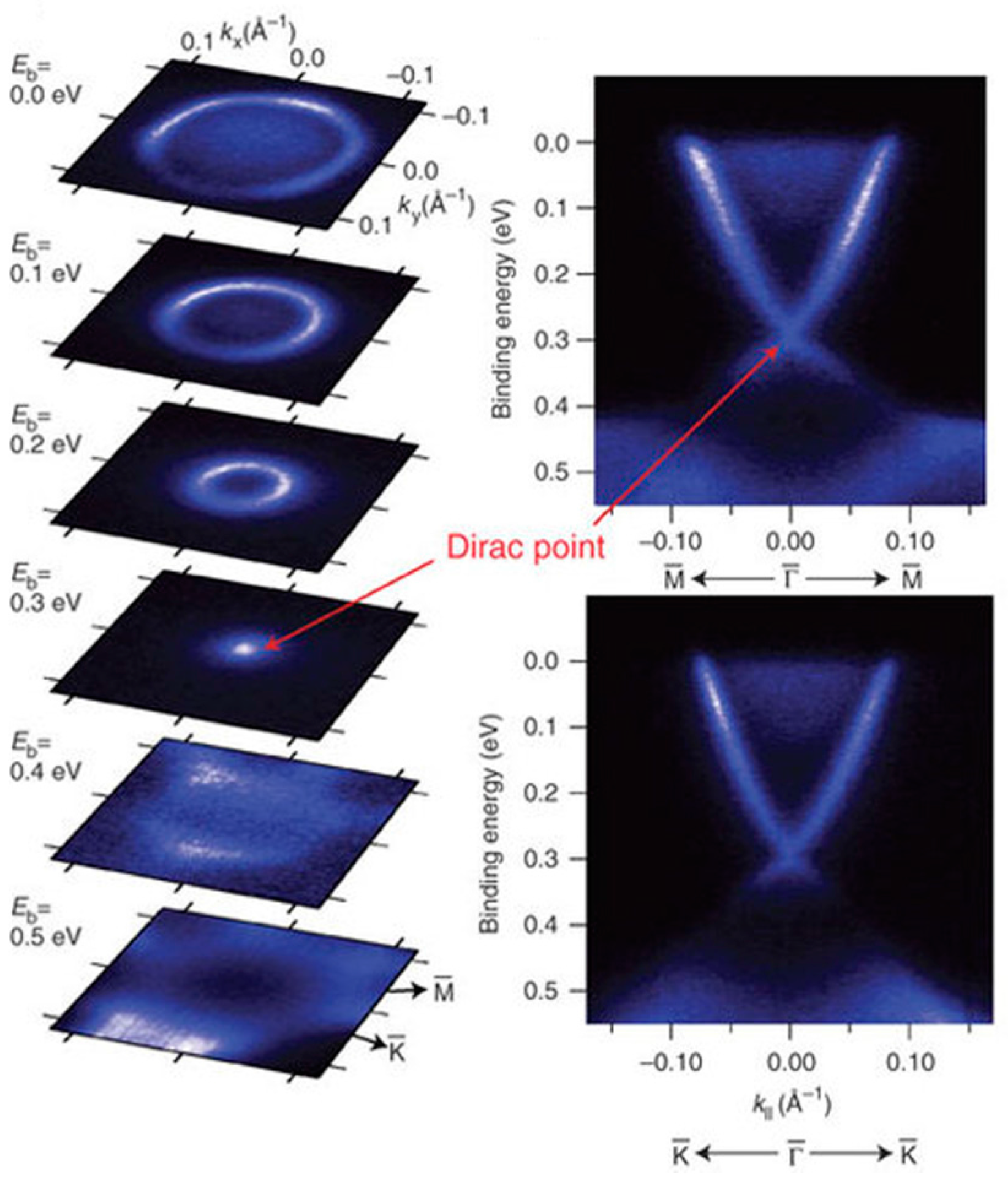
2.1.2. Electrical Properties/ARPES

The growth parameters discussed in Section 2.1.1 have yielded good-quality films and serve as a baseline for comparing different growth methods. For electrical device applications, the most important film characteristics are carrier mobility and concentration. An ideal topological insulator will have unimpeded electron flow through the surface states and no bulk carriers, so the MBE grown films should display high mobility and low carrier concentration. Using standard growth parameters, mobilities of 500–1000 cm2/Vs are usually reported with corresponding sheet densities in the mid 1013 cm−2. While these findings are promising, they all demonstrate the presence of non-topological carriers upon exposure to atmosphere and suggest a Fermi level residing in the bulk conduction band. This can be confirmed by angle resolved photoemission spectroscopy (ARPES) studies of the films. ARPES measures photoelectrons emitted after excitation via soft x-ray to map the electron distribution (and therefore the band structure) in a material relative to the Fermi level. It is an extremely surface sensitive measurement that is able to show the bulk bands, the topological surface states, and whether the Fermi level lies in the band gap. ARPES results confirm that even the best films grown via K-cell on sapphire substrates have their Fermi level pinned at best near the bottom of the conduction band. A typical ARPES scan of Bi2Se3 is shown in Figure 6.

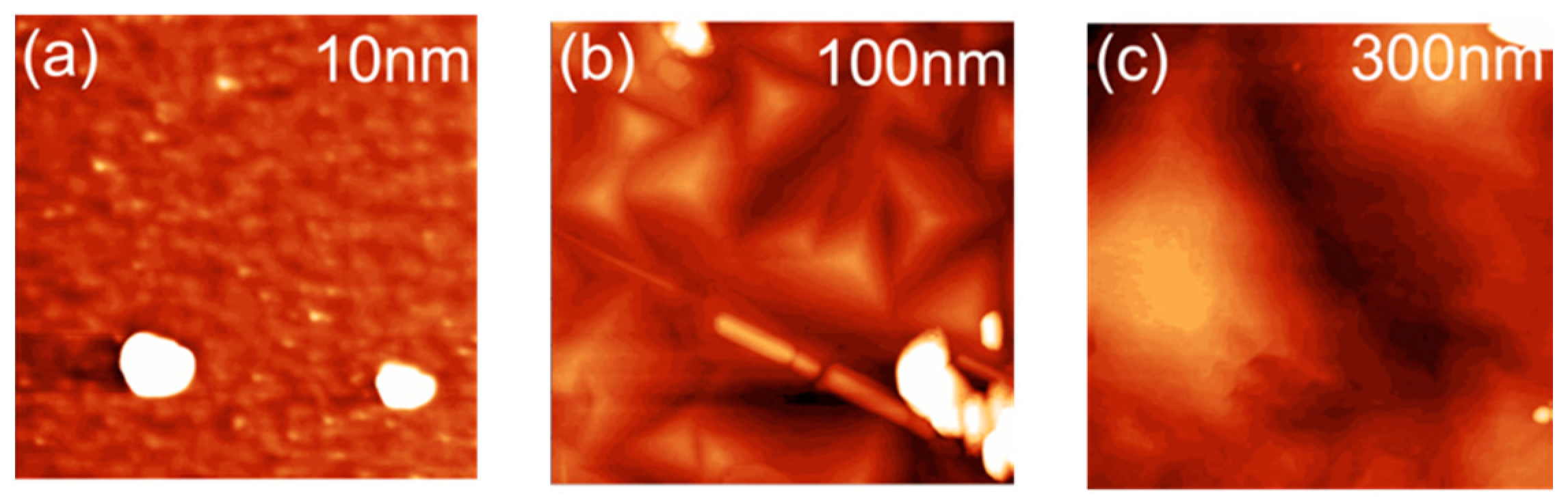
2.1.3. Atomic Force Microscopy

AFM scans done on Bi2Se3 films typically exhibit pyramid structures, as shown in Figure 7. The pyramids are likely caused by the rotational symmetry of the triangular in-plane lattice of the Bi2Se3 film, allowing islands to nucleate in different orientations, creating twining and other structural defects. Growth on vicinal or rough surfaces forces the nucleated islands to align along step edges and reduces twin defects [57]. Films with the best electrical properties tend to have fewer yet larger pyramids. This can be attributed to different growth conditions. When the surface mobility during growth is high enough, the bismuth and selenium adatoms have time to diffuse to the most energetically favorable positions. This will reduce the number of vacancy defects (improving electrical properties) and allow individual domains to grow larger (resulting in fewer but lager pyramids). If surface mobility is low, due to a low substrate temperature or high growth rate, adatoms will have less time to find favorable positions and more vacancy defects and pyramids will form. In very thin films (6–20 nm), Bi2Se3 tends to form many small triangular terraces, which is indicative of island formation in the early stages of growth. Island formation, or Volmer-Weber growth, is due to the domination of adatom-adatom interactions over adatom-substrate interactions. As films become thicker, the islands grow and merge, leading to fewer but larger pyramids. This is indicative of a switch to step flow growth along the edges of the terraces. The changeover to step flow growth indicates that the adatoms have a higher mobility on a completed Bi2Se3 QL than on the substrate, most likely due to the van der Waals bonding between QLs.

2.1.4. Substrate Choice

As previously mentioned, the van der Waals bonding between QLs allows Bi2Se3 to be grown on a wide range of substrates regardless of lattice mismatch. This is an extremely useful property for incorporating TIs into devices or studying their optical or electrical properties. Substrate choice is extremely customizable for specific applications. Growth parameters on different substrates tend to be very similar, with the largest differences being substrate preparation and temperature during growth. For example, growth on GaAs (111)B [36] and GaAs (001) [63,64] is best when a slightly higher substrate temperature is used than for growth on sapphire. Using these substrates also requires more careful substrate preparation, including desorption of the surface oxide layer in an arsenic flux followed by growth of a GaAs a buffer layer to create an extremely flat surface. These growth parameters yielded films with carrier densities of 8.06 × 1018 cm−3 to 4 × 1019 cm−3 and mobilities in the range ∼100−∼1000 cm2/(Vs). Similar results have been found for growths on Si(111), SiO2/Si, GaN [42], BaF2, InP, SrTiO3, and graphene [65,66]. An overview of film properties as a function of substrate choice can been seen in Table 1. Below, interesting findings and substrates for unique applications will be discussed in greater detail.
A study of TIs grown on InP with varying substrate surface roughness provided valuable insight into the effect of substrate roughness on TI film quality [34]. The study showed that substrates with rougher surfaces led to fewer twin boundaries and decreased surface roughness in the TI films. These results led to the conclusion that Bi2Se3 aligns itself to rough substrates by beginning growth in the hollows. While this does help to decrease twin defects, it also increases antiphase domain boundaries since not all of the hollows will be of equal depth. Xie et al. also did studies on InP(111) that support this finding [67]. When substrates were prepared to have large flat terraces, the Bi2Se3 film grew via island nucleation and twin domains were observed. However, on rougher substrates, Bi2Se3 films grew via a step flow growth method, and single-domain films were consistently observed. The strong interaction between InP substrates and Bi2Se3 films has led Guo et al. to suggest that these films are not grown by van der Waals epitaxy at all [38]. It may be that the low lattice mismatch between Bi2Se3 and InP (~3%) allows the substrate to have a greater influence on the subsequent film growth. These findings suggest that a film patterned to have controlled roughness of equal depth across the substrate would result in a film with very few structural defects. Growing on vicinal substrates has yielded similar results, with the step edges serving as nucleation points and forcing an orientation in the initial Bi2Se3 layer. Growth on vicinal Si(111) resulted in a mobility of~1600 cm2·V−1·s−1 and a 3D carrier concertation of ~5 × 1018 cm−3, as compared to ~1200 cm2· V−1· s−1 and ~3 × 1019 cm−3 on nonvicinal Si(111) by the same group [57].
Silicon is an attractive choice of substrate material for TI films due to its prevalence in electronic devices. One difficulty in using silicon is the presence of dangling bonds after the removal of the native oxide. If the dangling bonds are left unpassivated before TI growth begins, a layer of SiSe2 may form at the substrate interface [40] or a single crystal Bi2Se3 film may never be achieved [42]. One way to passivate the dangling bonds is to expose the film to a bismuth or selenium flux after the oxide is removed but before the TI growth begins. While bismuth exposure only provides a slight improvement over passivated Si films [42], selenium exposure has shown very promising results given the correct conditions. Bansal et al. found that a substrate temperature of approximately 100 °C during selenium exposure produced a self-limiting selenium passivation layer leading to an atomically sharp interface with the substrate [40]. Selenium passivation has also been successfully demonstrated on GaAs [68] and SiO2/Si films. Another approach to surface passivation is the growth of a buffer layer with a layered structure, such as GaSe, ZnSe, or In2Se3. The latter in particular has shown very promising results due to its similar structure and small lattice misfit (~3.4) to Bi2Se3 [69]. Even when substrate passivation is not needed, using an In2Se3/(BixIn1−x)2Se3 buffer layer has resulted in greatly improved electrical properties. The use of such a buffer between a sapphire substrate and a Bi2Se3 film resulted in 2D sheet densities as low as 1–3 × 1012 cm–2, allowing for the first successful observation of the Quantum Hall Effect in Bi2Se3 films [44]. However, incorporating a buffer layer can prove challenging if growth temperatures for the buffer layer and the TI film differ greatly. This is especially important for growth on Si substrates, which require a substrate temperature as low as 150 °C for Bi2Se3 growth [39]. For an overview of silicon passivation and buffer layers for Bi2Se3, see Wang et al. [42]. The methods used to prepare silicon substrates for good growths shed light on the importance of the substrate/film interface for the growth of good TI films, despite the use of van der Waals epitaxy. Applying similar techniques to other substrates may allow Bi2Se3 to be grown on an even wider variety of substrates.
Finally, dielectric SiO2/Si substrates have been widely used to back gate Bi2Se3 flakes [90,91,92], prompting many attempts to directly grow on these substrates [73,74,93]. Although the amorphous nature of SiO2/Si would hinder traditional MBE growth, Bi2Se3 can still be grown by taking advantage of van der Waals epitaxy. Like silicon substrates, the SiO2 surface has dangling bonds which must be passivated before growth, usually through an initial exposure to a selenium flux. By using a selenium capping layer to protect the film, a sheet density of ∼1.5  ±  0.04 × 1013/cm2 at low temperatures was reported, implying the Fermi level is close to the edge of the conduction band. More importantly, a carrier concentration as low as ∼3.5  × 1012/cm2 was achieved by applying a gate voltage of −170 V. A large enhancement of the peak resistance and the saturation of the sheet density suggest that this gate voltage fully depleted the bulk carriers and transport properties are now dominated by the topological surface states [74]. Controllable switching between dominating bulk or surface states is an important step toward real device applications.

2.1.5. Cracking Source
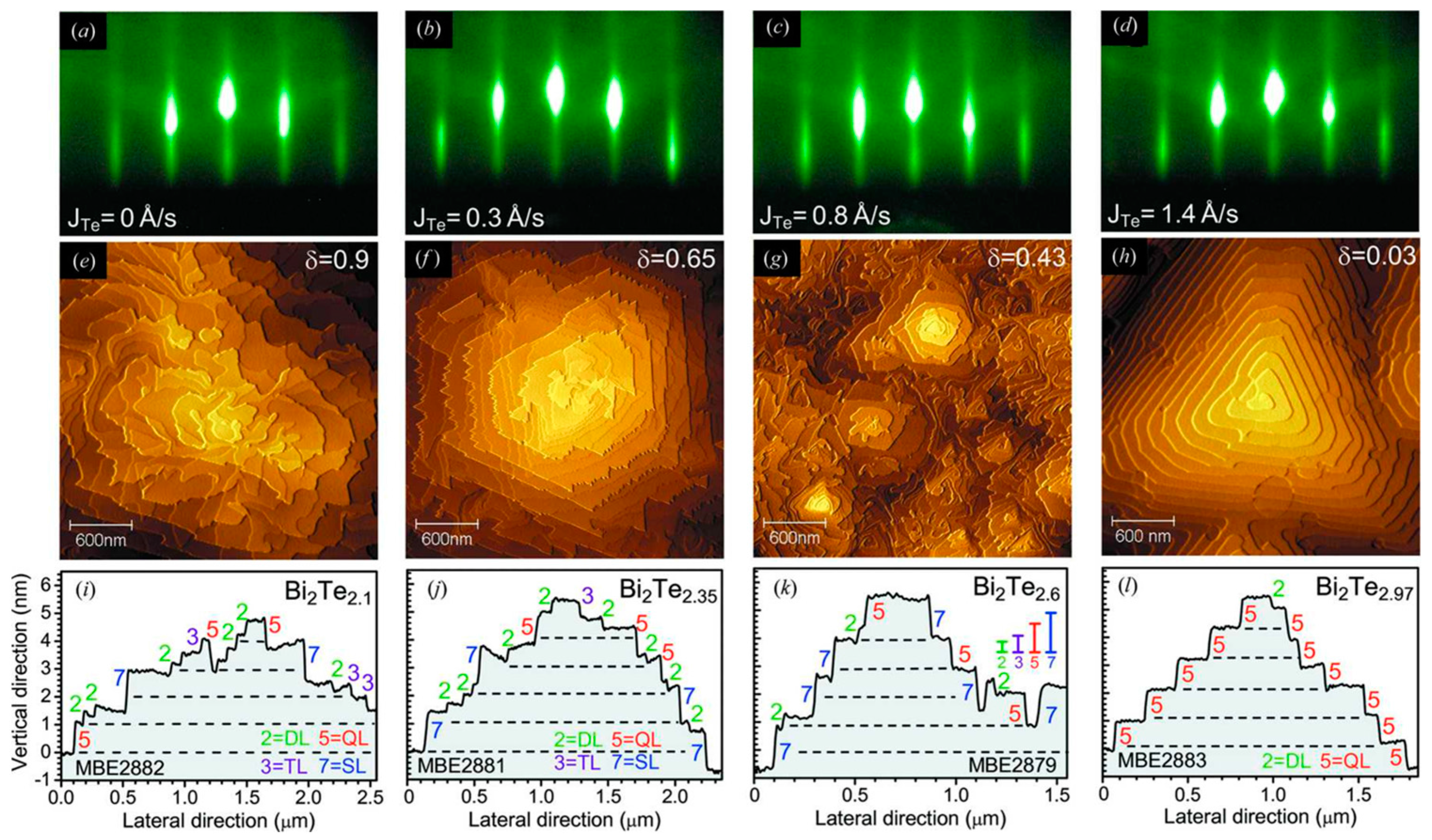
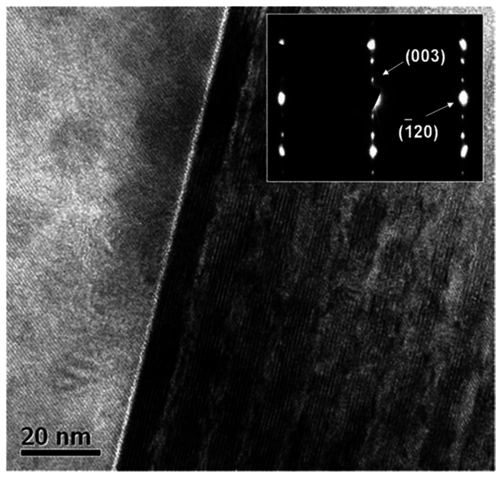
As discussed in Section 2.1.1, traditional K-cell selenium sources evaporate large molecules which are inefficiently incorporated into the films during growth, necessitating large selenium to bismuth ratios to create high quality films. Using a cracking source helps to overcome this problem by using a second heating zone held much hotter than the bulk evaporation zone or through the use of a radio-frequency cracker [94,95]. The cooler bulk evaporation zone is used to control the flux, while the large molecules that evaporate from the bulk are thermally cracked into monomers, dimers, and trimers in the cracking zone. These small molecules can be incorporated much more readily into the films, allowing Se:Bi ratios as low as 4:1 to be used while still achieving electrical properties comparable to samples grown via K-cell. While traditionally-grown films are prone to electrical aging effects, films grown with a cracker source have been demonstrated to maintain their electrical properties over a span of 60 days [62]. Better incorporation of selenium during growth is theorized to result in a smaller density of selenium vacancies, prohibiting oxygen from diffusing into the film as readily as in conventionally grown films.

2.2. Bi2Te3

Unlike the case of Bi2Se3, most growths of Bi2Te3 have been conducted on Si(111) substrates [83,96,97,98,99,100]. As discussed in Section 2.1.4, silicon substrates have dangling bonds which must be satisfied before growth can occur. As shown by Borisova et al. [41], these bonds can be terminated using a monolayer of Te upon which Bi2Te3 can nucleate in one of six possible orientations. The van der Waals bonding between the Te monolayer used to passivate the silicon substrate and the Bi2Te3 overlayer leads to a fully relaxed film within the first or second monolayer. In Situ x-ray scattering measurements by Liu et al. corroborate this finding and show the formation of a Te buffer layer in Te rich growth conditions even when the surface was not purposefully passivated [101]. Growth begins by the formation of many triangular islands which are only weakly bonded to the surface and are thus able to laterally diffuse along the surface. As film thickness increases, these islands coalesce until the substrate is completely covered, at which point the growth proceeds in a step flow mode, resulting in a similar pyramid structure as in Bi2Se3. This abrupt change in growth mode suggests that the diffusion length of adatoms is much larger on a completed QL than on the substrate. Much as in Bi2Se3 growths, growth of a high quality first QL is perhaps the most important factor in producing good films. Growing via van der Waals epitaxy allow for the use of substrates with large lattice mismatches, however controlling the initial nucleation is vital for reduction of defects and creation of an interface capable of supporting topological states. A counterintuitive advantage of silicon substrates is therefore their dangling bonds, which can be passivated by a tellurium monolayer, producing a surface that will support the growth of high-quality Bi2Te3.
If the substrate chosen does not have dangling bonds that can be satisfied with a Te monolayer, a two-step growth can be used to improve the interface at the substrate. High-quality topological insulators have been demonstrated on both sapphire [102,103] and SrTiO3 [104] using a two-step growth method. A nucleation layer is first deposited at a low substrate temperature (~190C) and then slowly annealed to the higher growth temperature (~230C), after which the rest of the film is deposited. After growth, the film is annealed at the growth temperature for an additional 30 minutes. This method resulted in films with a flatter morphology and reduced 3D growth defects than single-step TI growths. High-quality films have been grown on a number of different substrates including GaAs(001) [63], GaAs(111)B [36], GaN [105], graphene [65], amorphous fused silica [106], and mica (110) [86,107]. It is possible that adapting the two-step growth method will facilitate bulk insulating Bi2Te3 films on a wide variety of substrates.
Several studies of Bi2Te3 grown on BaF2 [80,108] have reported that small Te/Bi BEP ratios during growth led to the formation of bismuth bilayers between QLs, resulting in either the BiTe or Bi4Te3 phases in addition to or in place of the desired Bi2Te3 TI phase. Both alternate phases have considerably lower mobilities and higher carrier concentrations than Bi2Te3. In addition, neither phase shows evidence of the TI surface states. It is, therefore, extremely important to ensure the correct phase has been grown when studying these materials. The formation of alternate phases is most likely due to growth conditions with a deficit of tellurium. Fulop et al. [81] found that a beam equivalent pressure ratio below 17 favored the growth of Bi4Te3, though this growth was not conducted using a cracking source. When Steiner et al. [85] studied Bi2Te3-δ (where δ is the Te deficit) they found that δ close to 0 produced the most uniform quintuple layer steps despite good streaky reflection high energy electron diffraction (RHEED) being present for δ from 1 to 0, as shown in Figure 8. Therefore, RHEED may not be a reliable metric for achieving the correct composition. In addition, it is best to err on the tellurium-rich side of the phase diagram to insure the best film growth.
Li et al. report that the ideal condition for growing low carrier density Bi2Te3 thin films is a Te-rich growth environment where the bismuth Knudsen cell temperature is greater than the silicon substrate temperature which is greater than or equal to the tellurium Knudsen cell temperature (Tbi > TSi ≥ TTe) [99]. Keeping the substrate temperature equal to or above the tellurium cell temperature insures that Te2 molecules do not stick to the growth surface and film growth only occurs in the presence of a Bi flux. With the right growth conditions, carrier densities of ~1012 cm−2 and mobilities of 4600 cm2/Vs have been achieved, as calculated from ARPES data [51].
Finally, Wang et al. [109] demonstrated that it is possible to transition from n-type to p-type doped films by varying substrate temperature. Using a silicon substrate and a growth temperature below 580 K, films were n-type doped. Substrate temperatures between 580 K and 620 K produced relatively insulating films, while films grown above 620 K were p-type. In all cases, the carrier type was determined by monitoring the position of the Fermi energy with respect to the Dirac point through ARPES measurements performed in vacuum; no electrical measurements were performed. At high temperatures, the growth regime is step flow. Tellurium adatoms will have high mobility on the growth surface, increasing the probability of two adatoms combining to from Te2 and outgassing from the films. This results in a Te poor growth environment where Bi-on-Te antisite defects (acceptors) have a high probability of forming. At lower substrate temperatures the growth regime changes to layer by layer, as demonstrated by the presence of RHEED oscillations, and Te-on-Bi (donor) becomes the primary defect. The ability to control the transition from p-type to n-type films without the introduction of dopants is extremely useful for future device applications.

2.3. Sb2Te3

MBE-grown Sb2Te3 has not been as widely studied as either Bi2Se3 or Bi2Te3 and is most extensively studied as part of a ternary compound or heterostructure. As discussed Section 3 and Section 4, the intrinsic p-type doping of Sb2Te3 makes it an ideal candidate for alloying with n-type Bi2Se3 or Bi2Te3 to create net undoped films or for use in heterostructures to create p-n junctions. The reported ideal growth parameters for Sb2Te3 vary widely. Growth rates range from 0.2–2 QL/min, substrate temperatures from 200–320℃, and Te:Sb flux ratios from 2:1 to 20:1. Successful growths have been reported on many substrates including CdTe(111)B [88], graphene [110], sapphire (0001) [111], SiO2 [79], prestructured Si(111) SOI [82], and vicinal GaAs (111) (both A and B terminated) [89]. Where available, the electrical properties for each substrate are listed in Table 1. Bulk insulating Sb2Te3 has been demonstrated on Si(111) 7 × 7 substrates with robust TI surfaces states in films as thin as 6 QL [52]. While Bi2Se3 requires a minimum of 6 QL to display TI behavior, Sb2Te3 requires only 5 QL to form gapless surface states [52].
While the ideal growth parameters are still being debated, there have been several studies on the effect of growth parameters on defect types. Using scanning tunneling microscopy (STM) in conjunction with density functional theory (DFT) calculations, Jiang et al. [110] studied vacancy and antisite defects in Sb2Te3. These STM images are shown in Figure 9. They found that Sb vacancies are the primary source of doping for films grown at temperatures below ~200 °C. Unlike the case of Bi2Se3 or Bi2Te3, where Bi exists mostly in its atomic form, Sb exists mostly as a tetramer (Sb4) if a cracking source is not used. Due to its low mobility, Sb tends to form clusters on the growth surface. At low growth temperatures, this mobility is further reduced and Te is less likely to reevaporate, leading to Te-rich conditions and an increase in Sb vacancies. At higher temperatures, SbTe antisite defects on the outer Te sites become the dominant defect. Both defects types are acceptors, leading to the characteristic p-type doping observed in these films. Carrier concentration can be minimized by carefully selecting the substrate temperature during growth.
Kim et al. [88] conducted a similar study by looking at the effect for Te:Sb flux ratio on the electronic properties and c-axis lattice constant of Sb2Te3 films. Bulk Sb2Te3 has a lattice constant of 30.458 Å. In thin films at flux ratios below 3:1, the lattice constant varies from 30.572 to 30.385 Å, while above 3:1, it decreases to between 30.385 to 30.404 Å. This can be explained by a switch from TeSb to SbTe antisite defects. Sb is a larger atom than Te, so when it occupies a Te site, the lattice constant will increase to accommodate it. When Te on Sb defects start to dominate, the lattice constant decreases in response to the smaller atoms. Room temperature Hall measurements reveal the best electrical properties at a flux ratio of 3.6:1. Here the mobility has its maximum value of 279 cm2·V−1·s−1 and the 3D carrier concentration has its minimum value of 7.48 × 1018 cm−3. Both of these studies highlight the importance of understanding defect formation as a guide to finding the best growth parameters.

2.4. A Discussion on Carrier Density Determination

Many of the most interesting applications for topological insulator films are in electronic devices. This necessitates films that exhibit conductivity only through the surface states with few to no trivial carriers and a high mobility of the topological carriers. Unfortunately, many reports on the quality of TI films show only ARPES data, from which the authors extract a variety of information such as the position of the Fermi energy with respect to the Dirac point as well as the overall carrier density and mobility. Many of these ARPES measurements are performed in vacuum immediately following growth or on freshly-cleaved surfaces. While APRES is an excellent technique for characterizing the surface band structure of TI films, it is our opinion that ARPES measurements are of limited utility for determining the electrical quality of TI films. ARPES is inherently a surface-sensitive technique and generally only samples the first few layers of any material. This is, of course, quite useful for understanding the properties of the surfaces of TI films including the dispersion of the topological states, the presence or absence of a trivial band-bending 2DEG, and the position of the surface Fermi energy. However, this small penetration depth means that ARPES measurements are not able to probe the bulk behavior of a material. When discussing electrical conductivity, understanding the behavior of the bulk of the sample is crucial to understanding the overall properties. In this regard, traditional Hall measurements provide a much clearer picture of the carrier density and mobility in the film. High-field Schubnikov-de Haas measurements and low-field Hall measurement using a parallel conduction model have also been used to good effect to separate electrical contributions from the various conducting channels in TI films and crystals [112,113,114]. In addition, electrical measurements tend to be performed after exposure to air, giving a measurement that is more relevant to those wishing to create electronic devices based on TIs. In Table 1 we therefore put more emphasis on carrier density and mobility reports as determined using electrical measurements than those determined from ARPES analyses. For a comprehensive discussion of the electrical properties of TI films, including the role of surface accumulation and depletion layers, the reader is referred to reference [115].

3. Ternary Materials (E.G. Bi2(Se1–xTex)3, (BixSb1–x)2Te3)

MBE-grown binary TIs have been widely explored, but the ideal bulk-insulating state remains difficult to achieve. Recently, a variety of studies on ternary compounds Bi2(TexSe1−x)3 and (BixSb1−x)2Te3 have been performed in an attempt to further reduce the bulk conductance of TI films
Compared with Bi2Se3 or Bi2Te3, Bi2Te2Se is predicted to be much more bulk-insulating due to its -Te-Bi-Se-Bi-Te- quintuple unit structures. It not only limits the formation of Se vacancies but also suppresses the Bi/Te antisite defects [116]. Bi2Te2Se single crystals [117] and nanostructures [118] have already been widely explored, but reports on MBE growth of Bi2(TexSe1−x)3 alloys are still very limited. Y. Tung et al. [116] systematically studied the growth conditions of Bi2(TexSe1−x)3 in an MBE system. They successfully grew Bi2(TexSe1−x)3 on a sapphire substrate with a substrate temperature at 290 °C. The composition was tuned by varying the Se:Te flux ratio. The ARPES data clearly indicated that the Fermi level moved downward to the bottom of the conduction band at the composition around Bi2Te2Se. Their study supports the idea of reducing bulk carrier density by growing Bi2(TexSe1−x)3 alloys. However, no electrical measurements were performed, making it difficult to determine the bulk carrier density in these films. Despite the difficulty in growing, it is still possible to make more improvements based on this work. Choosing a more lattice matched substrate to reduce defects, or controlling the growth conditions more carefully are both possible ways to make further progress.
According to the band structure of pure Bi2Te3 and Sb2Te3 shown in Figure 10, Bi2Te3 is n-type doped due to Te vacancies while Sb2Te3 is p-type doped due to Sb/Te antisite defects. Therefore, it may be possible to tune the bulk carrier density and the position of the Fermi level by alloying the two compounds. Among the reports of (BixSb1−x)2Te3, the tuning of the Dirac point with composition was widely observed, but the exact composition where the carrier density was minimized is still under debate. Zhang et al. [119] engineered the band structure of the TI films by the MBE growth of (BixSb1−x)2Te3 alloys on sapphire substrates. The ARPES data indicated that the Fermi energy moved across the Dirac point as the Sb content was increased. The minimum bulk carrier sheet density was 1.4 × 1012 cm−2 obtained at x = 0.96. J. Kellner et al. [120] reported that among their films grown on highly doped Si(111) substrates, the Fermi level crosses the Dirac point at x = 0.94. X. He et al. [121] reported MBE grown (BixSb1−x)2Te3 on SrTiO3 substrates. In their work, a sheet density as low as 3 × 1012 cm−2 was obtained at around x = 0.5. Similar to their result, an Sb content of 0.47 was found to minimize the bulk conductance in a study on the surface spin polarizing behavior of (BixSb1−x)2Te3 grown on GaAs (111)B substrates [122]. C. Weyrich et al. [123] grew (BixSb1–x)2Te3 with various Sb content on Si(111) substrates. They reported the lowest sheet carrier density of 5 × 1012 cm−2 with an Sb content of 0.42. There clearly exists a dispute on the critical Sb content which is typically found to be either around 0.5 or around 0.9. This disagreement may be attributed to a difference in growth conditions or substrate choice, but further research is required to consistently obtain bulk insulating TI films. However, the existing data clearly shows that alloying TI materials can result in improved film properties and shows one possible way of obtaining the bulk insulating materials needed for many device applications. The ability to precisely control flux ratios and growth dynamics make MBE an excellent technique for growing these high quality films.

4. Heterostructures and Superlattices

MBE is also a good method to grow layered structures such as heterostructures and superlattices. Heterostructures include any structure with two or more dissimilar crystalline materials with sharp interfaces between them. Superlattices are periodic structures of two or more material layers. By controlling the material composition, layer thickness, or doping densities of each layer, the electronic and optical properties of the whole structure can be modified. For heterostructures and superlattices that include TI components, the unique surface states of the TI layers generate many interesting phenomena at the interfaces. Recently, there have been a variety of theoretical calculations and experimental realizations of heterostructures or superlattices that combine TIs with other kinds of materials. In this section, we will discuss the progress in TI heterostructure and superlattices grown by MBE.
As previously discussed in Section 3, the alloying of p-type and n-type binary topological insulators can result in samples with a reduced bulk conductivity. In addition to growing ternary alloys, topological insulator p-n junctions have also been grown, typically using the binary compounds Sb2Te3/Bi2Te3. Sb2Te3 tends to be p-type doped due to Sb/Te antisite defects, while Bi2Te3 tends to be n-type doped due to Te vacancies. Zeng et al. [89] grew Bi2Te3 and Sb2Te3 on GaAs (111) substrates successfully and pointed out the possibility to grow an Sb2Te3/Bi2Te3 p-n junction. Their work demonstrated that non-vincinal GaAs substrates produce higher quality Q2Te3 (Q = Sb, Bi) films than vicinal substrates. Sb2Te3/Bi2Te3 heterostructures on Si(111) substrates were first grown by Eschbach et al. [124]. By changing the thickness of Sb2Te3 layer, they were able to tune the chemical potential in the Bi2Te3 underlayer. ARPES data revealed that Dirac cone surface states still exist at the surface of Sb2Te3. Another group also reported Sb2Te3/Bi2Te3 heterostructures grown on Si(111) [125]. They found that ternary compounds formed at the interfaces due to Sb/Bi diffusion between layers. The tunability of bulk carrier density in Bi2Te3 layer via variation of Sb2Te3 layer thickness was also demonstrated. MBE-grown p-n junctions in TI films show great promise for studying novel quantum phenomena as well as potential applications in spintronics.
In addition to growing binary TI heterostructures, TI materials can also be grown in combination with other semiconductor or band insulator materials. Currently, the most promising band insulator material is In2Se3, which has the same QL structure as Bi2Se3, a relatively low lattice mismatch (~3.4%), and a reasonably large bandgap of ~1.3 eV. A study on MBE grown In2Se3/Bi2Se3 superlattices revealed that by tuning the thickness of TI layer, the transport of the whole material could switch between 2D and 3D [126]. Wang et al. [127] grew Bi2Se3/In2Se3 superlattices on Si(111) substrates with good film uniformity and sharp interfaces. The TEM image in Figure 11 showed clear interfaces between layers of their samples. More importantly, they were able to switch In2Se3 and Bi2Se3 growth by switching In and Bi fluxes while the Se flux was kept unchanged. Brahlek et al. [128] developed a superlattice system by sandwiching a layer of In2Se3 between two layers of Bi2Se3. By varying the thickness of the interlayer, the coupling between the two TI layers could be tuned from strongly coupled to totally decoupled. Using (InxBi1−x)2Se3 as the interlayer gave similar results. By tuning the indium composition from 1 down to 0.3, the coupling strength between bordering TI layers gradually increased at fixed interlayer thickness. These studies clearly revealed not only the eligibility of In2Se3 or (InxBi1−x)2Se3 as a buffer layer in Bi2Se3 growth, but also the tunability of transport properties.
In addition to band insulators, II-VI semiconductor layers have also been grown in combination with TI materials. These structures are of interest since superlattices contain multiple buried topological/trivial interfaces, allowing the intrinsic transport behavior to be observed even after the film was removed from the MBE chamber. In addition, employing the II–VI family enables band structure engineering, resulting in devices with a variety of band gaps and band alignments between the TI layers and the normal materials. This material class also allows for the creation of multiple types of band alignment within the semiconductor layers, enabling unique functionality in the TI heterostructure device. The first attempt at a TI/II–VI heterostructure used ZnSe as the semiconductor layer due to its relatively small lattice mismatch with Bi2Se3(~3.2%) [129]. Unfortunately, a rough interface between the Bi2Se3 and the ZnSe was observed under high resolution SEM, making this heterostructure unsuitable for applications. This first attempt was followed by the growth of II–VI alloys by Zhiyi Chen et al. [130]. They grew ZnxCd1−xSe/Bi2Se3, and ZnxCdyMg1−x−ySe/Bi2Se3 superlattices on sapphire substrates. Tuning the composition in the II–VI layer results in layers that are lattice matched to Bi2Se3, hence reducing the strain at the interface. They reported that Zn0.49Cd0.51Se and Zn0.23Cd0.25Mg0.52Se layers had improved quality relative to ZnSe. Another work by the same group reported that in MBE grown Zn0.49Cd0.51Se/Bi2Se3 superlattices, a single topological Dirac cone per TI layer was realized [28]. Leveraging the wide range of band gaps and band alignments in II–VI materials lattice-matched to TIs opens the door to the creation of multifunctional devices.
In addition to the creation of heterostructures using traditional insulators and semiconductors, TIs can also be layered with magnetic insulators (MIs). In this case, the surface state of TI could become gapped due to the breaking of time reversal symmetry (TRS) through exchange coupling with the MI. Luo et al. [131] calculated a series of heterostructures of Bi2Se3 and magnetic or antiferromagnetic insulators. In their study, the Bi2Se3/MnSe heterostructure was concluded to be the most ideal for relatively strong exchange coupling and a simple surface band structure. An experimental study on Bi2Se3/MnSe heterostructures supported this prediction. Matetskiy et al. [132] revealed that in the MBE-grown Bi2Se3/MnSe heterostructure, an energy gap of 90 meV is observed at the TI surface state, possibly due to the breaking of TRS. More complicated materials have also been attempted, including a (BixSb1−x)2Te3/yttrium iron garnet (YIG) heterostructure. This sample was made by directly growing (BixSb1−x)2Te3 onto a YIG substrate [133]. YIG was chosen as an under-layer because of its relatively large bulk band gap (2.85 eV). The advantage of such a system is its tunability in the magnetic properties at the interface.
Newer materials, including 2D materials, have also been grown in proximity to TI materials. Chang et al. [134] engineered the band structure of Bi2Se3 by growing another 2D material atop it. They investigated two types of structures: Bi2Se3 or Sb2Te3 grown on a graphene terminated 6H-silicon carbide (0001) substrate covered by 1 QL of Bi2Te3, and Bi2Se3 covered by 1 bilayer (BL) of Bi(111). ARPES data showed that both Bi2Te3/Bi2Se3 and Bi2Te3/Sb2Te3 showed similar surface states to Bi2Te3. This phenomenon can be understood by realizing that Bi2Se3, Sb2Te3, and Bi2Te3 all have the same Z2 number, which determines the surface topology [135]. However, the band structure changed significantly when the Bi2Se3 film was covered by BL Bi(111). ARPES data showed that the Dirac points from both BL Bi(111) and Bi2Se3 film coexisted, but the band dispersion was significantly modified. Another work on MBE grown BL Bi(111) atop Bi2Te3 heterostructures reported a shift of the Dirac point and a band bending effect at the Bi2Te3 and Bi BL interface [136]. They proposed the band structure of the system, and demonstrated the possibility of building band engineering devices based on such a structure.
Finally, it is predicted to be possible to find Majorana fermions if superconductivity can be introduced to TI through the proximity effect. Mei-Xiao Wang et al. [137] prepared atomically-flat Bi2Se3 films using MBE on top of 2H-NbSe2(0001), which is an s-wave superconductor substrate. This heterostructure exhibited a superconducting gap at the Bi2Se3 surface. A detailed ARPES study followed, indicating a deviation from idealized theoretical model in Bi2Se3/NbSe2 heterostructure due to the coexistence of multiple bands at the chemical potential [138]. Bi2Te3/NbSe2 heterostructures have also been reported [139,140]. These results showed that superconducting order was induced in the TI surface states through the proximity effect. In addition, evidence for a Majorana mode in a magnetic vortex in the Bi2Se3/NbSe3 heterostructure was observed. Su-Yang Xu et al. [141] reported epitaxially growing Bi2Se3 on a cuprate-superconductor Bi2Sr2CaCu2O8+δ (BSCCO) substrate. The electronic structure near the Fermi level of the system was studied. Their ARPES data provided evidence for the coexistence of two crystal phases in the film. However, despite the crystalline nature of the film, they were unable to observe the superconducting proximity effect in the TI film. This absence of proximity effect was confirmed by another study on MBE grown Bi2Se3/BSCCO heterostructure [142]. The absence of proximity effect, as stated in both studies, could be possibly attributed to a small superconducting coherence length, the presence of the topological surface state, and the different symmetries at the interface.

5. Conclusions

In conclusion, MBE is an excellent technique for the growth of TI thin films, heterostructures, and superlattices. The growth techniques used to obtain thin films of Bi2Se3, Bi2Te3, Sb2Te3, and alloys have been discussed in detail in this review, including the electrical properties that result when the substrate or growth conditions are changed. Although TIs are theorized to grow by van der Waals epitaxy, we find that there is significant evidence suggesting that the substrate strongly influences the quality of the resulting TI film. Choosing more lattice-matched substrates, careful preparation of the substrate surface, and the use of buffer layers have all resulted in an improvement in TI film properties. We believe that further experimentation will result in high structural quality films with a simultaneous low bulk carrier density, suitable for device applications. In addition, MBE is perfectly suited for the growth of a variety of superlattices and heterostructures, which can lead to new physics and new devices. We therefore conclude that there is a bright future for the MBE growth of the V2VI3 topological insulator family.

Acknowledgments

Theresa P. Ginley acknowledges funding from the University of Delaware Research Foundation, Grant No. 15A00862. Yong Wang and Stephanie Law are partially supported by the U.S. Department of Energy, Office of Science, Office of Basic Energy Sciences, under Award Number DE-SC0016380.

Author Contributions

Theresa P. Ginley, Yong Wang and Stephanie Law all wrote the paper.

Conflicts of Interest

The authors declare no conflict of interest.

References

  1. Chen, Y.L.; Analytis, J.G.; Chu, J.-H.; Liu, Z.K.; Mo, S.-K.; Qi, X.L.; Zhang, H.J.; Lu, D.H.; Dai, X.; Fang, Z.; et al. Experimental realization of a three-dimensional topological insulator, Bi2Te3. Science 2009, 325, 178–181. [Google Scholar] [CrossRef] [PubMed]
  2. Xia, Y.; Qian, D.; Hsieh, D.; Wray, L.; Pal, A.; Lin, H.; Bansil, A.; Grauer, D.; Hor, Y.S.; Cava, R.J.; et al. Observation of a large-gap topological-insulator class with a single Dirac cone on the surface. Nat. Phys. 2009, 5, 398–402. [Google Scholar] [CrossRef]
  3. Hsieh, D.; Xia, Y.; Qian, D.; Wray, L.; Dil, J.H.; Meier, F.; Osterwalder, J.; Patthey, L.; Checkelsky, J.G.; Ong, N.P.; et al. A tunable topological insulator in the spin helical Dirac transport regime. Nature 2009, 460, 1101–1105. [Google Scholar] [CrossRef] [PubMed] [Green Version]
  4. Hsieh, D.; Xia, Y.; Qian, D.; Wray, L.; Dil, J.H.; Osterwalder, J.; Patthey, L.; Fedorov, A.V.; Lin, H.; Bansil, A.; et al. Observation of Time-Reversal-Protected Single-Dirac-Cone Topological-Insulator States. Phys. Rev. Lett. 2009, 103, 146401. [Google Scholar] [CrossRef] [PubMed]
  5. Zhang, H.; Liu, C.-X.; Qi, X.-L.; Dai, X.; Fang, Z.; Zhang, S.-C. Topological insulators in Bi2Se3, Bi2Te3 and Sb2Te3 with a single Dirac cone on the surface. Nat. Phys. 2009, 5, 438–442. [Google Scholar] [CrossRef]
  6. Zhu, X.; Santos, L.; Howard, C.; Sankar, R.; Chou, F.C.; Chamon, C.; El-Batanouny, M. Electron-Phonon Coupling on the Surface of the Topological Insulator Bi2Se3 Determined from Surface-Phonon Dispersion Measurements. Phys. Rev. Lett. 2012, 108, 185501. [Google Scholar] [CrossRef] [PubMed]
  7. Pan, Z.-H.; Fedorov, A.V.; Gardner, D.; Lee, Y.S.; Chu, S.; Valla, T. Measurement of an Exceptionally Weak Electron-Phonon Coupling on the Surface of the Topological Insulator Bi2Se3 Using Angle-Resolved Photoemission Spectroscopy. Phys. Rev. Lett. 2012, 108, 187001. [Google Scholar] [CrossRef] [PubMed]
  8. Nemec, P.; Novák, V.; Sinova, J.; Jungwirth, T. Spin Hall Effect Transistor. Science 2010, 330, 1801–1804. [Google Scholar]
  9. Appelbaum, I.; Drew, H.D.; Fuhrer, M.S.; Appelbaum, I.; Drew, H.D.; Fuhrer, M.S. Proposal for a topological plasmon spin rectifier. Appl. Phys. Lett. 2011, 98, 23103. [Google Scholar] [CrossRef]
  10. Fu, L.; Kane, C. Superconducting Proximity Effect and Majorana Fermions at the Surface of a Topological Insulator. Phys. Rev. Lett. 2008, 100, 96407. [Google Scholar] [CrossRef] [PubMed]
  11. Akhmerov, A.R.; Nilsson, J.; Beenakker, C.W.J. Electrically Detected Interferometry of Majorana Fermions in a Topological Insulator. Phys. Rev. Lett. 2009, 102, 216404. [Google Scholar] [CrossRef] [PubMed]
  12. Hasan, M.Z.; Kane, C.L. Colloquium: Topological insulators. Rev. Mod. Phys. 2010, 82, 3045–3067. [Google Scholar] [CrossRef]
  13. Bernevig, B.A.; Zhang, S. Quantum Spin Hall Effect. Phys. Rev. Lett. 2006, 96, 106802. [Google Scholar] [CrossRef] [PubMed]
  14. Bernevig, B.A.; Hughes, T.L.; Zhang, S.-C. Quantum spin hall effect and topological phase transition in HgTe quantum wells. Science 2006, 314, 1757–1761. [Google Scholar] [CrossRef] [PubMed]
  15. Fu, L.; Kane, C.L.; Mele, E.J. Topological Insulators in Three Dimensions. Phys. Rev. Lett. 2007, 98, 106803. [Google Scholar] [CrossRef] [PubMed]
  16. Moore, J.E.; Balents, L. Topological invariants of time-reversal-invariant band structures. Phys. Rev. B 2007, 75, 121306(R). [Google Scholar] [CrossRef]
  17. Roy, R. Topological phases and the quantum spin Hall effect in three dimensions. Phys. Rev. B 2009, 79, 195322. [Google Scholar] [CrossRef]
  18. Hsieh, D.; Qian, D.; Wray, L.; Xia, Y.; Hor, Y.S.; Cava, R.J.; Hasan, M.Z. A topological Dirac insulator in a quantum spin Hall phase. Nature 2008, 452, 970–974. [Google Scholar] [CrossRef] [PubMed]
  19. Hsieh, D.; Xia, Y.; Wray, L.; Qian, D.; Pal, A.; Dil, J.H.; Osterwalder, J.; Meier, F.; Bihlmayer, G.; Kane, C.L.; et al. Observation of Unconventional Quantum Spin Textures in Topological Insulators. Science 2009, 323, 919–922. [Google Scholar] [CrossRef] [PubMed] [Green Version]
  20. Moore, J.E. The birth of topological insulators. Nature 2010, 464, 194–198. [Google Scholar] [CrossRef] [PubMed]
  21. Guo, Y.; Liu, Z.; Peng, H. A Roadmap for Controlled Production of Topological Insulator Nanostructures and Thin Films. Small 2015, 11, 3290–3305. [Google Scholar] [CrossRef] [PubMed]
  22. Chang, C.; Zhang, J.; Feng, X.; Shen, J.; Zhang, Z.; Guo, M.; Li, K.; Ou, Y.; Wei, P.; Wang, L.; et al. Experimental Observation of the Quantum Anomalous Hall Effect in a Magnetic Topological Insulator. Science 2013, 340, 167–171. [Google Scholar] [CrossRef] [PubMed]
  23. Qi, S.; Qiao, Z.; Deng, X.; Cubuk, E.D.; Chen, H.; Zhu, W.; Kaxiras, E.; Zhang, S.B.; Xu, X.; Zhang, Z. High-Temperature Quantum Anomalous Hall Effect in n-p Codoped Topological Insulators. Phys. Rev. Lett. 2016, 117, 056804. [Google Scholar] [CrossRef] [PubMed]
  24. Chang, C.Z.; Zhang, J.; Liu, M.; Zhang, Z.; Feng, X.; Li, K.; Wang, L.L.; Chen, X.; Dai, X.; Fang, Z.; et al. Thin films of magnetically doped topological insulator with carrier-independent long-range ferromagnetic order. Adv. Mater. 2013, 25, 1065–1070. [Google Scholar] [CrossRef] [PubMed]
  25. Chang, C.-Z.; Zhao, W.; Kim, D.Y.; Zhang, H.; Assaf, B.A.; Heiman, D.; Zhang, S.-C.; Liu, C.; Chan, M.H.W.; Moodera, J.S. High-precision realization of robust quantum anomalous Hall state in a hard ferromagnetic topological insulator. Nat. Mater. 2015, 14, 473–477. [Google Scholar] [CrossRef] [PubMed]
  26. Kou, X.; Guo, S.T.; Fan, Y.; Pan, L.; Lang, M.; Jiang, Y.; Shao, Q.; Nie, T.; Murata, K.; Tang, J.; et al. Scale-invariant quantum anomalous hall effect in magnetic topological insulators beyond the two-dimensional limit. Phys. Rev. Lett. 2014, 113, 137201. [Google Scholar] [CrossRef] [PubMed]
  27. Checkelsky, J.G.; Yoshimi, R.; Tsukazaki, A.; Takahashi, K.S.; Kozuka, Y.; Falson, J.; Kawasaki, M.; Tokura, Y. Trajectory of the anomalous Hall effect towards the quantized state in a ferromagnetic topological insulator. Nat. Phys. 2014, 10, 731–736. [Google Scholar] [CrossRef]
  28. Chen, Z.; Zhao, L.; Park, K.; Garcia, T.A.; Tamargo, M.C.; Krusin-Elbaum, L. Robust Topological Interfaces and Charge Transfer in Epitaxial Bi2Se3/II-VI Semiconductor Superlattices. Nano Lett. 2015, 15, 6365–6370. [Google Scholar] [CrossRef] [PubMed]
  29. Bianchi, M.; Guan, D.; Bao, S.; Mi, J.; Iversen, B.B.; King, P.D.C.; Hofmann, P. Coexistence of the topological state and a two-dimensional electron gas on the surface of Bi2Se3. Nat. Commun. 2010, 1, 128. [Google Scholar] [CrossRef] [PubMed]
  30. Koma, A.; Sunouchi, K.; Miyajima, T. Fabrication and characterization of heterostructures with subnanometer thickness. Microelectron. Eng. 1984, 2, 129–136. [Google Scholar] [CrossRef]
  31. Koma, A. Van der Waals epitaxy—A new epitaxial growth method for a highly lattice-mismatched system. Thin Solid Films 1992, 216, 72–76. [Google Scholar] [CrossRef]
  32. Momma, K.; Izumi, F. VESTA 3 for three-dimensional visualization of crystal, volumetric and morphology data. J. Appl. Crystallogr. 2011, 44, 1272–1276. [Google Scholar] [CrossRef]
  33. Chang, C.-Z.; He, K.; Wang, L.-L.; Ma, X.-C.; Liu, M.-H.; Zhang, Z.-C.; Chen, X.; Wang, Y.-Y.; Xue, Q.-K. Growth of quantum well films of topological insulator Bi2Se3 on insulating substrate. SPIN 2011, 1, 21. [Google Scholar] [CrossRef]
  34. Tarakina, N.V.; Schreyeck, S.; Luysberg, M.; Grauer, S.; Schumacher, C.; Karczewski, G.; Brunner, K.; Gould, C.; Buhmann, H.; Dunin-Borkowski, R.E.; et al. Suppressing Twin Formation in Bi2Se3 Thin Films. Adv. Mater. Interfaces 2014, 1, 1400134. [Google Scholar] [CrossRef]
  35. Kampmeier, J.; Borisova, S.; Plucinski, L.; Luysberg, M.; Mussler, G.; Grutzmacher, D. Suppressing Twin Domains in Molecular Beam Epitaxy Grown Bi2Te3 Topological Insulator Thin Films. Cryst. Growth Des. 2015, 15, 390–394. [Google Scholar] [CrossRef]
  36. Richardella, A.; Zhang, D.M.; Lee, J.S.; Koser, A.; Rench, D.W.; Yeats, A.L.; Buckley, B.B.; Awschalom, D.D.; Samarth, N. Coherent heteroepitaxy of Bi2Se3 on GaAs (111)B. Appl. Phys. Lett. 2010, 97, 262104. [Google Scholar] [CrossRef]
  37. Schreyeck, S.; Tarakina, N.V.; Karczewski, G.; Schumacher, C.; Borzenko, T.; Brüne, C.; Buhmann, H.; Gould, C.; Brunner, K.; Molenkamp, L.W.; et al. Molecular beam epitaxy of high structural quality Bi2Se3 on lattice matched InP(111) substrates. Appl. Phys. Lett. 2013, 102, 041914. [Google Scholar] [CrossRef]
  38. Guo, X.; Xu, Z.J.; Liu, H.J.C.; Zhao, B.; Dai, X.Q.; He, H.T.; Wang, J.N.; Liu, H.J.C.; Ho, W.K.; Xie, M.H. Single domain Bi2Se3 films grown on InP(111)A by molecular-beam epitaxy. Appl. Phys. Lett. 2013, 102, 151604. [Google Scholar] [CrossRef]
  39. He, L.; Xiu, F.; Wang, Y.; Fedorov, A.V.; Huang, G.; Kou, X.; Lang, M.; Beyermann, W.P.; Zou, J.; Wang, K.L. Epitaxial growth of Bi2Se3 topological insulator thin films on Si(111). J. Appl. Phys. 2011, 109, 103702. [Google Scholar] [CrossRef]
  40. Bansal, N.; Kim, Y.S.; Edrey, E.; Brahlek, M.; Horibe, Y.; Iida, K.; Tanimura, M.; Li, G.-H.; Feng, T.; Lee, H.-D.; et al. Epitaxial growth of topological insulator Bi2Se3 film on Si(111) with atomically sharp interface. Thin Solid Films 2011, 520, 224–229. [Google Scholar] [CrossRef]
  41. Borisova, S.; Krumrain, J.; Luysberg, M.; Mussler, G.; Grützmacher, D. Mode of Growth of Ultrathin Topological Insulator Bi2Te3 Films on Si(111) Substrates. Cryst. Growth Des. 2012, 12, 6098–6103. [Google Scholar] [CrossRef]
  42. Wang, Z.Y.; Li, H.D.; Guo, X.; Ho, W.K.; Xie, M.H. Growth characteristics of topological insulator Bi2Se3 films on different substrates. J. Cryst. Growth 2011, 334, 96–102. [Google Scholar] [CrossRef]
  43. Rathi, S.J.; Smith, D.J.; Drucker, J. Optimization of In2Se3/Si(111) Heteroepitaxy To Enable Bi2Se3/In2Se3 Bilayer Growth. Cryst. Growth Des. 2014, 14, 4617–4623. [Google Scholar] [CrossRef]
  44. Koirala, N.; Brahlek, M.; Salehi, M.; Wu, L.; Dai, J.; Waugh, J.; Nummy, T.; Han, M.-G.; Moon, J.; Zhu, Y.; et al. Record Surface State Mobility and Quantum Hall Effect in Topological Insulator Thin Films via Interface Engineering. Nano Lett. 2015, 15, 8245–8249. [Google Scholar] [CrossRef] [PubMed]
  45. Valdés Aguilar, R.; Wu, L.; Stier, A.V.; Bilbro, L.S.; Brahlek, M.; Bansal, N.; Oh, S.; Armitage, N.P. Aging and reduced bulk conductance in thin films of the topological insulator Bi2Se3. J. Appl. Phys. 2013, 113, 153702. [Google Scholar] [CrossRef]
  46. Bianchi, M.; Hatch, R.C.; Mi, J.; Iversen, B.B.; Hofmann, P. Simultaneous quantization of bulk conduction and valence states through adsorption of nonmagnetic impurities on Bi2Se3. Phys. Rev. Lett. 2011, 107, 086802. [Google Scholar] [CrossRef] [PubMed]
  47. King, P.D.C.; Hatch, R.C.; Bianchi, M.; Ovsyannikov, R.; Lupulescu, C.; Landolt, G.; Slomski, B.; Dil, J.H.; Guan, D.; Mi, J.L.; et al. Large Tunable Rashba Spin Splitting of a Two-Dimensional Electron Gas in Bi2Se3. Phys. Rev. Lett. 2011, 107, 096802. [Google Scholar] [CrossRef] [PubMed]
  48. Chen, C.; He, S.; Weng, H.; Zhang, W.; Zhao, L.; Liu, H.; Jia, X.; Mou, D.; Liu, S.; He, J.; et al. Robustness of topological order and formation of quantum well states in topological insulators exposed to ambient environment. Proc. Natl. Acad. Sci. USA 2012, 109, 3694–3698. [Google Scholar] [CrossRef] [PubMed]
  49. Benia, H.M.; Lin, C.; Kern, K.; Ast, C.R. Reactive Chemical Doping of the Bi2Se3 Topological Insulator. Phys. Rev. Lett. 2011, 107, 177602. [Google Scholar] [CrossRef] [PubMed]
  50. Bianchi, M.; Hatch, R.C.; Guan, D.; Planke, T.; Mi, J.; Iversen, B.B.; Hofmann, P. The electronic structure of clean and adsorbate-covered Bi2Se3: An angle-resolved photoemission study. Semicond. Sci. Technol. 2012, 27, 124001. [Google Scholar] [CrossRef]
  51. Hoefer, K.; Becker, C.; Rata, D.; Swanson, J.; Thalmeier, P.; Tjeng, L.H. Intrinsic conduction through topological surface states of insulating Bi2Te3 epitaxial thin films. Proc. Natl. Acad. Sci. USA 2014, 111, 14979–14984. [Google Scholar] [CrossRef] [PubMed]
  52. Wang, G.; Zhu, X.; Wen, J.; Chen, X.; He, K.; Wang, L.; Ma, X.; Liu, Y.; Dai, X.; Fang, Z.; et al. Atomically smooth ultrathin films of topological insulator Sb2Te3. Nano Res. 2010, 3, 874–880. [Google Scholar] [CrossRef]
  53. Plucinski, L.; Herdt, A.; Fahrendorf, S.; Bihlmayer, G.; Mussler, G.; Döring, S.; Kampmeier, J.; Matthes, F.; Bürgler, D.E.; Grützmacher, D.; et al. Electronic structure, surface morphology, and topologically protected surface states of Sb2Te3 thin films grown on Si(111). J. Appl. Phys. 2013, 113, 053706. [Google Scholar] [CrossRef]
  54. Pauly, C.; Bihlmayer, G.; Liebmann, M.; Grob, M.; Georgi, A.; Subramaniam, D.; Scholz, M.R.; Sánchez-Barriga, J.; Varykhalov, A.; Blügel, S.; et al. Probing two topological surface bands of Sb2Te3 by spin-polarized photoemission spectroscopy. Phys. Rev. B Condens. Matter Mater. Phys. 2012, 86, 235106. [Google Scholar] [CrossRef]
  55. Seixas, L.; Abdalla, L.B.; Schmidt, T.M.; Fazzio, A.; Miwa, R.H. Topological states ruled by stacking faults in Bi2Se3 and Bi2Te3. J. Appl. Phys. 2013, 113, 023705. [Google Scholar] [CrossRef]
  56. Tarakina, N.V.; Schreyeck, S.; Borzenko, T.; Schumacher, C.; Karczewski, G.; Brunner, K.; Gould, C.; Buhmann, H.; Molenkamp, L.W. Comparative Study of the Microstructure of Bi2Se3 Thin Films Grown on Si(111) and InP(111) Substrates. Cryst. Growth Des. 2012, 12, 1913–1918. [Google Scholar] [CrossRef]
  57. Li, H.D.; Wang, Z.Y.; Kan, X.; Guo, X.; He, H.T.; Wang, Z.; Wang, J.N.; Wong, T.L.; Wang, N.; Xie, M.H. The van der Waals epitaxy of Bi2Se3 on the vicinal Si(111) surface: An approach for preparing high-quality thin films of a topological insulator. New J. Phys. 2010, 12, 103038. [Google Scholar] [CrossRef]
  58. Takagaki, Y.; Jenichen, B. Epitaxial growth of Bi2Se3 layers on InP substrates by hot wall epitaxy. Semicond. Sci. Technol. 2012, 27, 35015. [Google Scholar] [CrossRef]
  59. Alpichshev, Z.; Biswas, R.R.; Balatsky, A.V.; Analytis, J.G.; Chu, J.-H.; Fisher, I.R.; Kapitulnik, A. STM Imaging of Impurity Resonances on Bi2Se3. Phys. Rev. Lett. 2012, 108, 206402. [Google Scholar] [CrossRef] [PubMed]
  60. Analytis, J.G.; Chu, J.-H.; Chen, Y.; Corredor, F.; Mcdonald, R.D.; Shen, Z.X.; Fisher, I.R. Bulk Fermi surface coexistence with Dirac surface state in Bi2Se3: A comparison of photoemission and Shubnikov–de Haas measurements. Phys. Rev. B 2010, 81, 205407. [Google Scholar] [CrossRef]
  61. Berkowitz, J. Equilibrium Composition of Selenium Vapor; the Thermodynamics of the Vaporization of HgSe, CdSe, and SrSe. J. Chem. Phys. 1966, 45, 4289. [Google Scholar] [CrossRef]
  62. Ginley, T.P.; Law, S. Growth of Bi2Se3 topological insulator films using a selenium cracker source. J. Vac. Sci. Technol. B Nanotechnol. Microelectron. Mater. Process. Meas. Phenom. 2016, 34, 02L105. [Google Scholar] [CrossRef]
  63. Liu, X.; Smith, D.J.; Fan, J.; Zhang, Y.-H.; Cao, H.; Chen, Y.P.; Leiner, J.; Kirby, B.J.; Dobrowolska, M.; Furdyna, J.K. Structural properties of Bi2Te3 and Bi2Se3 topological insulators grown by molecular beam epitaxy on GaAs(001) substrates. Appl. Phys. Lett. 2011, 99, 171903. [Google Scholar] [CrossRef]
  64. Liu, X.; Smith, D.J.; Cao, H.; Chen, Y.P.; Fan, J.; Zhang, Y.-H.; Pimpinella, R.E.; Dobrowolska, M.; Furdyna, J.K. Characterization of Bi2Te3 and Bi2Se3 topological insulators grown by MBE on (001) GaAs substrates. J. Vac. Sci. Technol. B 2012, 30, 02B103. [Google Scholar] [CrossRef]
  65. Kim, N.; Lee, P.; Kim, Y.Y.; Kim, J.S.; Kim, Y.Y.; Noh, D.Y.; Yu, S.U.; Chung, J.; Kim, K.S. Persistent Topological Surface State at the Interface of Bi2Se3 Film Grown on Patterned Graphene. ACS Nano 2014, 8, 1154–1160. [Google Scholar] [CrossRef] [PubMed]
  66. Song, C.-L.; Wang, Y.Y.-L.; Jiang, Y.-P.; Zhang, Y.; Chang, C.-Z.; Wang, L.; He, K.; Chen, X.; Jia, J.-F.; Wang, Y.Y.-L.; et al. Topological insulator Bi2Se3 thin films grown on double-layer graphene by molecular beam epitaxy. Appl. Phys. Lett. 2010, 97, 143118. [Google Scholar] [CrossRef]
  67. Xie, M.-H.; Guo, X.; Xu, Z.-J.; Ho, W.-K. Molecular-beam epitaxy of topological insulator Bi2Se3 (111) and (221) thin films. Chin. Phys. B 2013, 22, 68101. [Google Scholar] [CrossRef]
  68. Pashley, M.D.; Li, D. Control of the Fermi-level position on the GaAs(001) surface: Se passivation. J. Vac. Sci. Technol. A 1994, 12, 1848. [Google Scholar] [CrossRef]
  69. Emziane, M.; Marsillac, S.; Bernède, J.C. Preparation of highly oriented α-In2Se3 thin films by a simple technique. Mater. Chem. Phys. 2000, 62, 84–87. [Google Scholar] [CrossRef]
  70. Jing, Y.; Huang, S.; Zhang, K.; Wu, J.; Guo, Y.; Peng, H.; Liu, Z.; Xu, H.Q. Weak antilocalization and electron–electron interaction in coupled multiple-channel transport in a Bi2Se3 thin film. Nanoscale 2016, 8, 1879–1885. [Google Scholar] [CrossRef] [PubMed]
  71. Wang, X.; He, X.; Guan, T.; Liao, J.; Lin, C.; Wu, K.; Li, Y.; Zeng, C. Transport properties of topological insulator Bi2Se3 thin films in tilted magnetic fields. Physica E 2012, 46, 236–240. [Google Scholar] [CrossRef]
  72. Li, C.H.; van't Erve, O.M.J.; Robinson, J.T.; Liu, Y.; Li, L.; Jonker, B.T. Electrical detection of charge-current-induced spin polarization due to spin-momentum locking in Bi2Se3. Nat. Nanotechnol. 2014, 9, 218–224. [Google Scholar] [CrossRef] [PubMed]
  73. Jerng, S.-K.; Joo, K.; Kim, Y.S.Y.; Yoon, S.-M.; Lee, J.H.; Kim, M.; Kim, J.S.; Yoon, E.; Chun, S.-H.; Kim, Y.S.Y. Ordered growth of topological insulator Bi2Se3 thin films on dielectric amorphous SiO2 by MBE. Nanoscale 2013, 5, 10618. [Google Scholar] [CrossRef] [PubMed]
  74. Liu, Y.H.; Chong, C.W.; Jheng, J.L.; Huang, S.Y.M.; Huang, J.C.A.; Li, Z.; Qiu, H.; Huang, S.Y.M.; Marchenkov, V.V. Gate-tunable coherent transport in Se-capped Bi2Se3 grown on amorphous SiO2/Si. Appl. Phys. Lett. 2015, 107, 12106. [Google Scholar] [CrossRef]
  75. Tabor, P.; Keenan, C.; Urazhdin, S.; Lederman, D.; Urazdhin, S.; Lederman, D. Molecular beam epitaxy and characterization of thin Bi2Se3 films on Al2O3 (110). Appl. Phys. Lett. 2011, 99, 13111. [Google Scholar] [CrossRef]
  76. Glinka, Y.D.; Babakiray, S.; Lederman, D. Plasmon-enhanced electron-phonon coupling in Dirac surface states of the thin-film topological insulator Bi2Se3. J. Appl. Phys. 2015, 118, 135713. [Google Scholar] [CrossRef]
  77. He, L.; Xiu, F.; Yu, X.; Teague, M.; Jiang, W.; Fan, Y.; Kou, X.; Lang, M.; Wang, Y.; Huang, G.; et al. Surface-Dominated Conduction in a 6 nm thick Bi2Se3 Thin Film. Nano Lett. 2012, 12, 1486–1490. [Google Scholar] [CrossRef] [PubMed]
  78. Park, B.C.; Kim, T.-H.; Sim, K.I.; Kang, B.; Kim, J.W.J.H.; Cho, B.; Jeong, K.-H.; Cho, M.-H.; Kim, J.W.J.H. Terahertz single conductance quantum and topological phase transitions in topological insulator Bi2Se3 ultrathin films. Nat. Commun. 2015, 6, 6552. [Google Scholar] [CrossRef] [PubMed]
  79. Aabdin, Z.; Peranio, N.; Winkler, M.; Bessas, D.; König, J.; Hermann, R.P.; Böttner, H.; Eibl, O. Sb2Te3 and Bi2Te3 Thin Films Grown by Room-Temperature MBE. J. Electron. Mater. 2012, 41, 1493–1497. [Google Scholar] [CrossRef]
  80. Caha, O.; Dubroka, A.; Humlíček, J.; Holý, V.; Steiner, H.; Ul-Hassan, M.; Sánchez-Barriga, J.; Rader, O.; Stanislavchuk, T.N.; Sirenko, A.A.; et al. Growth, Structure, and Electronic Properties of Epitaxial Bismuth Telluride Topological Insulator Films on BaF2(111) Substrates. Cryst. Growth Des. 2013, 13, 3365–3373. [Google Scholar] [CrossRef]
  81. Fülöp, A.; Song, Y.; Charpentier, S.; Shi, P.; Ekström, M.; Galletti, L.; Arpaia, R.; Bauch, T.; Lombardi, F.; Wang, S. Phase transition of bismuth telluride thin films grown by MBE. Appl. Phys. Express 2014, 7, 45503. [Google Scholar] [CrossRef]
  82. Kampmeier, J.; Weyrich, C.; Lanius, M.; Schall, M.; Neumann, E.; Mussler, G.; Schäpers, T.; Grützmacher, D. Selective area growth of Bi2Te3 and Sb2Te3 topological insulator thin films. J. Cryst. Growth 2016, 443, 38–42. [Google Scholar] [CrossRef]
  83. Liu, H.W.; Yuan, H.T.; Fukui, N.; Zhang, L.; Jia, J.F.; Iwasa, Y.; Chen, M.W.; Hashizume, T.; Sakurai, T.; Xue, Q.K. Growth of Topological Insulator Bi2Te3 Ultrathin Films on Si(111) Investigated by Low-Energy Electron Microscopy. Cryst. Growth Des. 2010, 10, 4491–4493. [Google Scholar] [CrossRef]
  84. Roy, A.; Guchhait, S.; Sonde, S.; Dey, R.; Pramanik, T.; Rai, A.; Movva, H.C.P.; Colombo, L.; Banerjee, S.K. Two-dimensional weak anti-localization in Bi2Te3 thin film grown on Si(111)-(7 × 7) surface by molecular beam epitaxy. Appl. Phys. Lett. 2013, 102, 163118. [Google Scholar] [CrossRef]
  85. Steiner, H.; Volobuev, V.; Caha, O.; Bauer, G.; Springholz, G.; Holý, V. Structure and composition of bismuth telluride topological insulators grown by molecular beam epitaxy. J. Appl. Crystallogr. 2014, 47, 1889–1900. [Google Scholar] [CrossRef]
  86. Wang, K.L.; Liu, Y.; Wang, W.; Meyer, N.; Bao, L.H.; He, L.; Lang, M.R.; Chen, Z.G.; Che, X.Y.; Post, K.; et al. High-quality Bi2Te3 thin films grown on mica substrates for potential optoelectronic applications. Appl. Phys. Lett. 2013, 103, 31605. [Google Scholar] [CrossRef]
  87. Yu, X.; He, L.; Lang, M.; Jiang, W.; Xiu, F.; Liao, Z.; Wang, Y.; Kou, X.; Zhang, P.; Tang, J.; et al. Separation of top and bottom surface conduction in Bi2Te3 thin films. Nanotechnology 2013, 24, 15705. [Google Scholar] [CrossRef] [PubMed]
  88. Kim, Y.; DiVenere, A.; Wong, G.K.L.; Ketterson, J.B.; Cho, S.; Meyer, J.R. Structural and thermoelectric transport properties of Sb2Te3 thin films grown by molecular beam epitaxy. J. Appl. Phys. 2002, 91, 715–718. [Google Scholar] [CrossRef]
  89. Zeng, Z.; Morgan, T.A.; Fan, D.; Li, C.; Hirono, Y.; Hu, X.; Zhao, Y.; Lee, J.S.; Wang, J.; Wang, Z.M.; et al. Molecular beam epitaxial growth of Bi2Te3 and Sb2Te3 topological insulators on GaAs (111) substrates: A potential route to fabricate topological insulator p–n junction. AIP Adv. 2013, 3, 72112. [Google Scholar] [CrossRef]
  90. Kong, D.; Dang, W.; Cha, J.J.; Li, H.; Meister, S.; Peng, H.; Liu, Z.; Cui, Y. Few-Layer Nanoplates of Bi2Se3 and Bi2Te3 with Highly Tunable Chemical Potential. Nano Lett. 2010, 10, 2245–2250. [Google Scholar] [CrossRef] [PubMed]
  91. Steinberg, H.; Gardner, D.R.; Lee, Y.S.; Jarillo-Herrero, P. Surface State Transport and Ambipolar Electric Field Effect in Bi2Se3 Nanodevices. Nano Lett. 2010, 10, 5032–5036. [Google Scholar] [CrossRef] [PubMed] [Green Version]
  92. Checkelsky, J.G.; Hor, Y.S.; Cava, R.J.; Ong, N.P. Bulk Band Gap and Surface State Conduction Observed in Voltage-Tuned Crystals of the Topological Insulator Bi2Se3. Phys. Rev. Lett. 2011, 106, 196801. [Google Scholar] [CrossRef] [PubMed]
  93. Bansal, N.; Koirala, N.; Brahlek, M.; Han, M.-G.; Zhu, Y.; Cao, Y.; Waugh, J.; Dessau, D.S.; Oh, S. Robust topological surface states of Bi2Se3 thin films on amorphous SiO2/Si substrate and a large ambipolar gating effect. Appl. Phys. Lett. 2014, 104, 241606. [Google Scholar] [CrossRef]
  94. Zhang, L.; Hammond, R.; Dolev, M.; Liu, M.; Palevski, A.; Kapitulnik, A. High quality ultrathin Bi2Se3 films on CaF2 and CaF2/Si by molecular beam epitaxy with a radio frequency cracker cell. Appl. Phys. Lett. 2012, 101, 153105. [Google Scholar] [CrossRef]
  95. Lee, J.J.; Schmitt, F.T.; Moore, R.G.; Vishik, I.M.; Ma, Y.; Shen, Z.X. Intrinsic ultrathin topological insulators grown via molecular beam epitaxy characterized by in-situ angle resolved photoemission spectroscopy. Appl. Phys. Lett. 2012, 101, 13118. [Google Scholar] [CrossRef]
  96. Park, J.; Soh, Y.-A.; Aeppli, G.; Bland, S.R.; Zhu, X.-G.; Chen, X.; Xue, Q.-K.; Grey, F. Crystal structure and epitaxy of Bi2Te3 films grown on Si. Appl. Phys. Lett. 2012, 101, 221910. [Google Scholar] [CrossRef]
  97. Chen, X.; Ma, X.-C.; He, K.; Jia, J.-F.; Xue, Q.-K. Molecular Beam Epitaxial Growth of Topological Insulators. Adv. Mater. 2011, 23, 1162–1165. [Google Scholar] [CrossRef] [PubMed]
  98. Krumrain, J.; Mussler, G.; Borisova, S.; Stoica, T.; Plucinski, L.; Schneider, C.M.; Grützmacher, D. MBE growth optimization of topological insulator Bi2Te3 films. J. Cryst. Growth 2011, 324, 115–118. [Google Scholar] [CrossRef]
  99. Li, Y.-Y.; Wang, G.; Zhu, X.-G.; Liu, M.-H.; Ye, C.; Chen, X.; Wang, Y.-Y.; He, K.; Wang, L.-L.; Ma, X.-C.; et al. Intrinsic topological insulator Bi2Te3 thin films on Si and their thickness limit. Adv. Mater. 2010, 22, 4002–4007. [Google Scholar] [CrossRef] [PubMed]
  100. Liu, Y.; Bian, G.; Miller, T.; Bissen, M.; Chiang, T.-C. Topological limit of ultrathin quasi-free-standing Bi2Te3 films grown on Si(111). Phys. Rev. B 2012, 85, 195442. [Google Scholar] [CrossRef]
  101. Liu, Y.; Wang, H.H.; Bian, G.; Zhang, Z.; Lee, S.S.; Fenter, P.A.; Tischler, J.Z.; Hong, H.; Chiang, T.C. Interfacial bonding and structure of Bi2Te3 topological insulator films on Si(111) determined by surface X-ray scattering. Phys. Rev. Lett. 2013, 110, 226103. [Google Scholar] [CrossRef] [PubMed]
  102. Plucinski, L.; Mussler, G.; Krumrain, J.; Herdt, A.; Suga, S.; Grützmacher, D.; Schneider, C.M. Robust surface electronic properties of topological insulators: Bi2Te3 films grown by molecular beam epitaxy. Appl. Phys. Lett. 2011, 98, 222503. [Google Scholar] [CrossRef]
  103. Harrison, S.E.; Li, S.; Huo, Y.; Zhou, B.; Chen, Y.L.; Harris, J.S. Two-step growth of high quality Bi2Te3 thin films on Al2O3 (0001) by molecular beam epitaxy. Appl. Phys. Lett. 2013, 102, 2011–2015. [Google Scholar] [CrossRef]
  104. Ngabonziza, P.; Heimbuch, R.; de Jong, N.; Klaassen, R.A.; Stehno, M.P.; Snelder, M.; Solmaz, A.; Ramankutty, S.V.; Frantzeskakis, E.; van Heumen, E.; et al. In situ spectroscopy of intrinsic Bi2Te3 topological insulator thin films and impact of extrinsic defects. Phys. Rev. B 2015, 92, 35405. [Google Scholar] [CrossRef]
  105. Xu, H.; Song, Y.; Gong, Q.; Pan, W.; Wu, X.; Wang, S. Raman spectroscopy of epitaxial topological insulator Bi2Te3 thin films on GaN substrates. Mod. Phys. Lett. B 2015, 29, 1550075. [Google Scholar] [CrossRef]
  106. Collins-McIntyre, L.J.; Wang, W.; Zhou, B.; Speller, S.C.; Chen, Y.L.; Hesjedal, T. Growth of Bi2Se3 and Bi2Te3 on amorphous fused silica by MBE. Phys. Status Solidi B 2015, 252, 1334–1338. [Google Scholar] [CrossRef]
  107. Rapacz, R.; Balin, K.; Wojtyniak, M.; Szade, J. Morphology and local conductance of single crystalline Bi2Te3 thin films on mica. Nanoscale 2015, 7, 16034–16038. [Google Scholar] [CrossRef] [PubMed]
  108. Fornari, C.I.; Rappl, P.H.O.; Morelhão, S.L.; Abramof, E. Structural properties of Bi2Te3 topological insulator thin films grown by molecular beam epitaxy on (111) BaF2 substrates. J. Appl. Phys. 2016, 119, 165303. [Google Scholar] [CrossRef]
  109. Wang, G.; Zhu, X.-G.; Sun, Y.-Y.; Li, Y.-Y.; Zhang, T.; Wen, J.; Chen, X.; He, K.; Wang, L.-L.; Ma, X.-C.; et al. Topological insulator thin films of Bi2Te3 with controlled electronic structure. Adv. Mater. 2011, 23, 2929–2932. [Google Scholar] [CrossRef] [PubMed]
  110. Jiang, Y.; Sun, Y.Y.; Chen, M.; Wang, Y.; Li, Z.; Song, C.; He, K.; Wang, L.; Chen, X.; Xue, Q.-K.; et al. Fermi-Level Tuning of Epitaxial Sb2Te3 Thin Films on Graphene by Regulating Intrinsic Defects and Substrate Transfer Doping. Phys. Rev. Lett. 2012, 108, 66809. [Google Scholar] [CrossRef] [PubMed]
  111. Chien, Y.-J.; Zhou, Z.; Uher, C. Growth and transport properties of Sb2−xVxTe3 thin films on sapphire substrates. J. Cryst. Growth 2005, 283, 309–314. [Google Scholar] [CrossRef]
  112. Taskin, A.A.; Sasaki, S.; Segawa, K.; Ando, Y. Manifestation of topological protection in transport properties of epitaxial Bi2Se3 thin films. Phys. Rev. Lett. 2012, 109, 066803. [Google Scholar] [CrossRef] [PubMed]
  113. Bansal, N.; Kim, Y.S.; Brahlek, M.; Edrey, E.; Oh, S. Thickness-Independent Transport Channels in Topological Insulator Bi2Se3 Thin Films. Phys. Rev. Lett. 2012, 109, 116804. [Google Scholar] [CrossRef] [PubMed]
  114. Xiong, J.; Luo, Y.; Khoo, Y.; Jia, S.; Cava, R.J.; Ong, N.P. High-field Shubnikov-de Haas oscillations in the topological insulator Bi2Te2Se. Phys. Rev. B Condens. Matter Mater. Phys. 2012, 86, 045314. [Google Scholar] [CrossRef]
  115. Brahlek, M.; Koirala, N.; Bansal, N.; Oh, S. Transport properties of topological insulators: Band bending, bulk metal-to-insulator transition, and weak anti-localization. Solid State Commun. 2015, 215, 54–62. [Google Scholar] [CrossRef]
  116. Tung, Y.; Chiang, Y.F.; Chong, C.W.; Deng, Z.X.; Chen, Y.C.; Huang, J.C.A.; Cheng, C.-M.M.; Pi, T.-W.W.; Tsuei, K.-D.D.; Li, Z.; et al. Growth and characterization of molecular beam epitaxy-grown Bi2Te3−xSex topological insulator alloys. J. Appl. Phys. 2016, 119, 55303. [Google Scholar] [CrossRef]
  117. Ren, Z.; Taskin, A.A.; Sasaki, S.; Segawa, K.; Ando, Y. Large bulk resistivity and surface quantum oscillations in the topological insulator Bi2Te2Se. Phys. Rev. B 2010, 82, 241306(R). [Google Scholar] [CrossRef]
  118. Cha, J.J.; Kong, D.; Hong, S.-S.; Analytis, J.G.; Lai, K.; Cui, Y. Weak antilocalization in Bi2(Se(x)Te(1−x))3 nanoribbons and nanoplates. Nano Lett. 2012, 12, 1107–1111. [Google Scholar] [CrossRef] [PubMed]
  119. Zhang, J.; Chang, C.; Zhang, Z.; Wen, J.; Feng, X.; Li, K.; Liu, M.; He, K.; Wang, L.; Chen, X.; et al. Band structure engineering in (Bi1−xSbx)2Te3 ternary topological insulators. Nat. Commun. 2011, 2, 574. [Google Scholar] [CrossRef] [PubMed]
  120. Kellner, J.; Eschbach, M.; Kampmeier, J.; Lanius, M.; Młyńczak, E.; Mussler, G.; Holländer, B.; Plucinski, L.; Liebmann, M.; Grützmacher, D.; et al. Tuning the Dirac point to the Fermi level in the ternary topological insulator (Bi1−xSbx)2Te3. Appl. Phys. Lett. 2015, 107, 251603. [Google Scholar] [CrossRef]
  121. He, X.; Li, H.; Chen, L.; Wu, K. Substitution-induced spin-splitted surface states in topological insulator (Bi1−xSbx)2Te3. Sci. Rep. 2015, 5, 8830. [Google Scholar] [CrossRef] [PubMed]
  122. Tang, J.; Chang, L.T.; Kou, X.; Murata, K.; Choi, E.S.; Lang, M.; Fan, Y.; Jiang, Y.; Montazeri, M.; Jiang, W.; et al. Electrical detection of spin-polarized surface states conduction in (Bi0.53Sb0.47)2Te3 topological insulator. Nano Lett. 2014, 14, 5423–5429. [Google Scholar] [CrossRef] [PubMed]
  123. Weyrich, C.; Drögeler, M.; Kampmeier, J.; Eschbach, M.; Mussler, G.; Merzenich, T.; Stoica, T.; Batov, I.E.; Schubert, J.; Plucinski, L.; et al. Growth, characterization, and transport properties of ternary (Bi1−xSbx)2Te3 topological insulator layers. J. Phys. Condens. Matter 2015, 28, 495501. [Google Scholar] [CrossRef] [PubMed]
  124. Eschbach, M.; Młyńczak, E.; Kellner, J.; Kampmeier, J.; Lanius, M.; Neumann, E.; Weyrich, C.; Gehlmann, M.; Gospodarič, P.; Döring, S.; et al. Realization of a vertical topological p–n junction in epitaxial Sb2Te3/Bi2Te3 heterostructures. Nat. Commun. 2015, 6, 8816. [Google Scholar] [CrossRef] [PubMed]
  125. Lanius, M.; Kampmeier, J.; Weyrich, C.; Kölling, S.; Schall, M.; Schüffelgen, P.; Neumann, E.; Luysberg, M.; Mussler, G.; Koenraad, P.M.; et al. pn Junctions in Ultrathin Topological Insulator Sb2Te3/Bi2Te3 Heterostructures Grown by Molecular Beam Epitaxy. Cryst. Growth Des. 2016, 16, 2057–2061. [Google Scholar] [CrossRef]
  126. Zhao, Y.; Liu, H.; Guo, X.; Jiang, Y.; Sun, Y.; Wang, H.; Wang, Y.; Li, H.-D.D.; Xie, M.-H.H.; Xie, X.-C.C.; et al. Crossover from 3D to 2D Quantum Transport in Bi2Se3/In2Se3 Superlattices. Nano Lett. 2014, 14, 5244–5249. [Google Scholar] [CrossRef] [PubMed]
  127. Wang, Z.Y.; Guo, X.; Li, H.D.; Wong, T.L.; Wang, N.; Xie, M.H. Superlattices of Bi2Se3/In2Se3: Growth characteristics and structural properties. Appl. Phys. Lett. 2011, 99, 023112. [Google Scholar] [CrossRef] [Green Version]
  128. Brahlek, M.J.; Koirala, N.; Liu, J.; Yusufaly, T.I.; Salehi, M.; Han, M.G.; Zhu, Y.; Vanderbilt, D.; Oh, S. Tunable inverse topological heterostructure utilizing (Bi1−xInx)2Se3 and multichannel weak-antilocalization effect. Phys. Rev. B 2016, 93, 125416. [Google Scholar] [CrossRef]
  129. Li, H.D.; Wang, Z.Y.; Guo, X.; Wong, T.L.; Wang, N.; Xie, M.H. Growth of multilayers of Bi2Se3/ZnSe: Heteroepitaxial interface formation and strain. Appl. Phys. Lett. 2011, 98, 043104. [Google Scholar] [CrossRef] [Green Version]
  130. Chen, Z.; Garcia, T.A.; Hernandez-Mainet, L.C.; Zhao, L.; Deng, H.; Krusin-Elbaum, L.; Tamargo, M.C. Molecular beam epitaxial growth and characterization of Bi2Se3/II-VI semiconductor heterostructures. Appl. Phys. Lett. 2014, 105, 242105. [Google Scholar] [CrossRef]
  131. Luo, W.; Qi, X.L. Massive Dirac surface states in topological insulator/magnetic insulator heterostructures. Phys. Rev. B 2013, 87. [Google Scholar] [CrossRef]
  132. Matetskiy, A.V.; Kibirev, I.A.; Hirahara, T.; Hasegawa, S.; Zotov, A.V.; Saranin, A.A. Direct observation of a gap opening in topological interface states of MnSe/Bi2Se3 heterostructure. Appl. Phys. Lett. 2015, 107, 091604. [Google Scholar] [CrossRef]
  133. Jiang, Z.; Chang, C.Z.; Tang, C.; Zheng, J.G.; Moodera, J.S.; Shi, J. Structural and proximity-induced ferromagnetic properties of topological insulator-magnetic insulator heterostructures. AIP Adv. 2016, 6, 055809. [Google Scholar] [CrossRef]
  134. Chang, C.Z.; Tang, P.; Feng, X.; Li, K.; Ma, X.C.; Duan, W.; He, K.; Xue, Q.K. Band Engineering of Dirac Surface States in Topological-Insulator-Based van der Waals Heterostructures. Phys. Rev. Lett. 2015, 115, 136801. [Google Scholar] [CrossRef] [PubMed]
  135. Kane, C.L.; Mele, E.J. Z2 topological order and the quantum spin hall effect. Phys. Rev. Lett. 2005, 95, 146802. [Google Scholar] [CrossRef] [PubMed]
  136. Chen, M.; Peng, J.P.; Zhang, H.M.; Wang, L.L.; He, K.; Ma, X.C.; Xue, Q.K. Molecular beam epitaxy of bilayer Bi(111) films on topological insulator Bi2Te3: A scanning tunneling microscopy study. Appl. Phys. Lett. 2012, 101, 081603. [Google Scholar] [CrossRef]
  137. Wang, M.-X.; Li, P.; Xu, J.-P.; Liu, Z.-L.; Ge, J.-F.; Wang, G.-Y.; Yang, X.; Xu, Z.-A.; Ji, S.-H.; Gao, C.L.; et al. Interface structure of a topological insulator/superconductor heterostructure. New J. Phys. 2014, 16, 123043. [Google Scholar] [CrossRef]
  138. Xu, S.-Y.; Alidoust, N.; Belopolski, I.; Richardella, A.; Liu, C.; Neupane, M.; Bian, G.; Huang, S.-H.; Sankar, R.; Fang, C.; et al. Momentum-space imaging of Cooper pairing in a half-Dirac-gas topological superconductor. Nat. Phys. 2014, 10, 943–950. [Google Scholar] [CrossRef]
  139. Xu, J.P.; Liu, C.; Wang, M.X.; Ge, J.; Liu, Z.L.; Yang, X.; Chen, Y.; Liu, Y.; Xu, Z.A.; Gao, C.L.; et al. Artificial topological superconductor by the proximity effect. Phys. Rev. Lett. 2014, 112, 217001. [Google Scholar] [CrossRef]
  140. Xu, J.P.; Wang, M.X.; Liu, Z.L.; Ge, J.F.; Yang, X.; Liu, C.; Xu, Z.A.; Guan, D.; Gao, C.L.; Qian, D.; et al. Experimental detection of a Majorana mode in the core of a magnetic vortex inside a topological insulator-superconductor Bi2Te3/NbSe2 heterostructure. Phys. Rev. Lett. 2015, 114, 017001. [Google Scholar] [CrossRef] [PubMed]
  141. Xu, S.Y.; Liu, C.; Richardella, A.; Belopolski, I.; Alidoust, N.; Neupane, M.; Bian, G.; Samarth, N.; Hasan, M.Z. Fermi-level electronic structure of a topological-insulator/cuprate-superconductor based heterostructure in the superconducting proximity effect regime. Phys. Rev. B 2014, 90, 085128. [Google Scholar] [CrossRef]
  142. Yilmaz, T.; Pletikosic, I.; Weber, A.P.; Sadowski, J.T.; Gu, G.D.; Caruso, A.N.; Sinkovic, B.; Valla, T. Absence of a proximity effect for a thin-films of a Bi2Se3 topological insulator grown on top of a Bi2Sr2CaCu2O8+δ cuprate superconductor. Phys. Rev. Lett. 2014, 113, 067003. [Google Scholar] [CrossRef] [PubMed]
Figure 1. Calculated band structure of Bi2Se3 showing the linear dispersion of the surface states. Reproduced with permission from Zhang et al., Nature Physics; published by Nature Publishing Group, 2009 [5].
Crystals 06 00154 g001
Figure 2. Crystal structure of tetradymite Bi2Se3 (other TI materials are similar). Bi atoms are large and shown in blue while Se atoms are smaller and shown in yellow. (a) Crystal structure along the a-b plane showing two quintuple layers with the van der Waals gap between them. (b) Crystal structure along the c-axis. Structure created with VESTA [32].
Crystals 06 00154 g002
Figure 3. Lattice constants of various substrates compared to lattice constants of binary TIs. For zincblende and cubic structures, the lattice constant of the (111) face is given. For wurtzite structures, graphene, In2Se3 and Al2O3, the lattice constant of the hexagonal (001) face is given.
Crystals 06 00154 g003
Figure 4. ARPES scans of bulk Bi2Se3 crystals taken at (a) 10 min, (b) 1 h, (c) 3 h and (d) 16 h after cleaving. As time passes, the Dirac point shifts lower and additional conduction band states from band bending become visible. (e) Magnification of the conduction band from (d) showing the Rashba split quantum well states. (f) Photoemission intensity at normal emission as a function of binding energy and kz acquired with a photon energy scan. Reproduced with permission from Bianchi et al., Semiconductor Science and Technology; published by IOP Science, 2012 [50].
Crystals 06 00154 g004
Figure 5. The two types of stacking faults (ISF, or intrinsic stacking fault, and ESF, or extrinsic stacking fault) possible in a TI film. Reproduced with permission from Seixas et al., Journal of Applied Physics; published by the American Institute of Physics, 2013 [55].
Crystals 06 00154 g005
Figure 6. ARPES measurement of bulk Bi2Se3(0001). The topological surface states can be seen as the bright lines crossing the bulk bandgap. Reproduced with permission from Bianchi et al., Nature Communications; published by Nature Publishing Group, 2010 [29].
Crystals 06 00154 g006
Figure 7. 2 × 2 μm atomic force microscopy images of Bi2Se3 films of thickness (a) 10 nm, (b) 100 nm, and (c) 300 nm. Color scale for (a) is 0–8 nm, for (b) is 0–10 nm, and for (c) is 0–60 nm. The triangular terraces grow larger and merge as the film becomes thicker. Reproduced with permission from Ginley et al., Journal of Vacuum Science and Technology B; published by the American Vacuum Society, 2016 [62].
Crystals 06 00154 g007
Figure 8. (ad) RHEED patterns for Bi2Te3 growth with varying Te flux as indicated. (eh) AFM images corresponding to the Bi2Te3 films grown with the parameters in panels (ad). (il) Step height measurements for the Bi2Te3 films indicating double layers (DL), triple layers (TL), quintuple layers (QL), and septuple layers (SL) Reproduced with permission from Steiner et al., Journal of Applied Crystallography; published by the International Union of Crystallography, 2014 [85].
Crystals 06 00154 g008
Figure 9. (a)–(c) Large-area STM images showing various types of defects in Sb2Te3, labeled from I to V with tunneling voltages of (a) 1.0 V, 50 pA; (b) 1.0 V, 50 pA; and (c) 0.4 V, 50 pA. (d) High-resolution STM images of defects labeled in (a)–(c) with tunneling conditions: (I) 0.2 V, 100 pA; (II) 0.1 V, 100 pA; (III) 0.2 V, 100 pA; (IV) −0.5 V, 50 pA; and (V) −1.0 V, 50 pA. (e),(f) Schematic drawings of Sb2Te3 (111) crystal structure showing positions of the defects. Te and Sb atoms are denoted by small (green) and large (pink) spheres, respectively. Note that, looking from the top, I is above V and IV is above II and III. Reproduced with permission from Jiang et al., Physical Review Letters; published by the American Physical Society, 2012 [110].
Crystals 06 00154 g009
Figure 10. (a) Crystal structure of (BixSb1−x)2Te3 alloy. Bi2Te3 tends to have a Fermi level above the Dirac point as shown by the band structure diagram in (b) while Sb2Te3 tends to have a Fermi level below the Dirac point as shown by the band structure diagram in (c). Alloys are predicted to have a Fermi level tunable across the Dirac point. Reproduced with permission from Zhang et al., Nature Communications; published by Nature Publishing Group, 2011 [119].
Crystals 06 00154 g010
Figure 11. TEM image of a 3 nm-In2Se3/7 nm-Bi2Se3 superlattice sample. Inset: Transmission electron diffraction data of the same sample. Reproduced with permission from Wang et al., Applied Physics Letters; published by the American Institute of Physics, 2011 [127].
Crystals 06 00154 g011
Table 1. Electrical properties of binary TIs. Where data was available, columns give TI material, the substrate on which it was grown, mobility (μ), sheet density (n2D), bulk density (n3D), film thickness (t), and temperature at which the electrical measurements were performed (T).
MaterialSubstrateμ
cm2/Vs
n2D
cm−2
n3D
cm−3
t
nm
T
K
Reference
Bi2Se3Mica4726.1 × 1013 10 [70]
Bi2Se3Graphene Intrinsic <10 [66]
Bi2Se3SrTiO3(111) 1.9–3.1 × 10¹³ 5–50 [71]
Bi2Se3Graphene and Al2O3(0001) ~1 × 101911–45 [72]
Bi2Se3InP(111)A3500 ~1 × 10¹⁸ 2[38]
Bi2Se3Si(111) Vicinal1600 5 × 10182002[57]
Bi2Se3Si(111) Flat1200 3 × 10192002[57]
Bi2Se3Si(111) 1.25  ×  1013 7200[39]
Bi2Se3SiO2 ~4  ×  1013 202[73]
Bi2Se3Graphene5000 [6] ~1.1 × 101940020[65]
Bi2Se3AlOx623∼3 × 10¹³ 100300[62]
Bi2Se3GaAs (111)B100−1000 8.06–40 × 1018 4.2[36]
Bi2Se3SiO2/Si ∼2.2 × 10¹³ 7 [74]
Bi2Se3Al2O3(110)150 9.4 × 10182013[75]
Bi2Se3Al2O3(0001) 0.5–3.5 × 10192–40 [76]
Bi2Se3Rough InP(111)B2000 9 × 10171004[34]
Bi2Se3CdS(0001)~4000 [6]~6 × 10¹¹ 62[77]
Bi2Se3CdS(0001)~400 [7]~1 × 10¹³ 62[77]
Bi2Se3Si (100)2880 [6]8.4 × 10¹⁰ 8 [78]
Bi2Se3Si (100)54 [8]4.5 × 10¹² 8 [78]
Bi2Te3 [1]SiO22.8 1 × 10²¹~100300[79]
Sb2Te3 [1]SiO242 2.4 × 10¹⁹ [9]~100300[79]
Bi2Te3 [1a]SiO280 2.7 x 10¹⁹~100300[79]
Sb2Te3 [1a]SiO2402 2.6 × 10¹⁹ [9]~100300[79]
Bi2Te3BaF2(111) 1.3 × 10¹⁹ [2][80]
Bi2Te3Si(111)1030 4.7 × 10¹⁹ [81]
Bi2Te3BaF2(111)2000–46002–4 × 10¹² 10–50[3][51]
Bi2Te3Prestructured Si(111) SOI1101.6 × 1014 [5][82]
Sb2Te3Prestructured Si(111) SOI6366.7 × 1013 [9] [5][82]
Bi2Te3Si(111) 7 × 10121.32 × 10195.3300[83]
Bi2Te3n-type Si(111)351.2 × 10¹⁴ 42[84]
Bi2Te3BaF2(111)1500 2–10 × 101835077[85]
Bi2Te3Mica48002.45 × 1012 4[4][86]
Bi2Te3GaAs(111)B 10.6 × 10¹² 2[87]
Sb2Te3CdTe(111)B279 7.48 × 10¹⁸~300290[88]
Sb2Te3V-GaAs(111)B781 9.13 × 10184001.8[89]
[1] Films were grown at room temperature, then annealed, as indicated with the [1a] superscript; [2] Calculated from Seebeck measurements; [3] Calculated from ARPES measurements; [4] Calculated from Schubnikov-de Haas measurements; [5] Data was taken at low temperature, no absolute value given; [6] Calculated for TI surface; [7] Calculated for impurity band; [8] Calculated for trivial quantum well states; [9] Carriers were majority p-type.

