
Temperature-Dependent X-ray Diffraction Measurements of Infrared Superlattices Grown by MBE


Abstract
:
1. Introduction
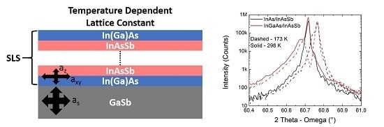
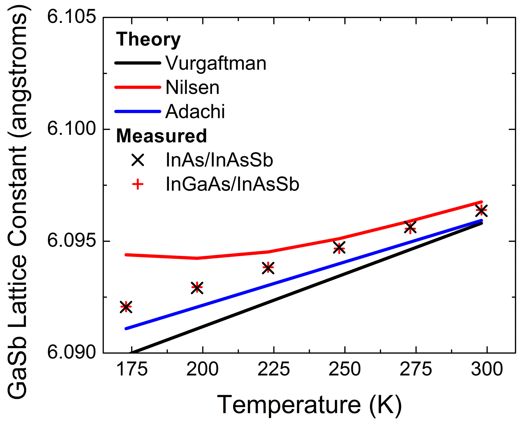
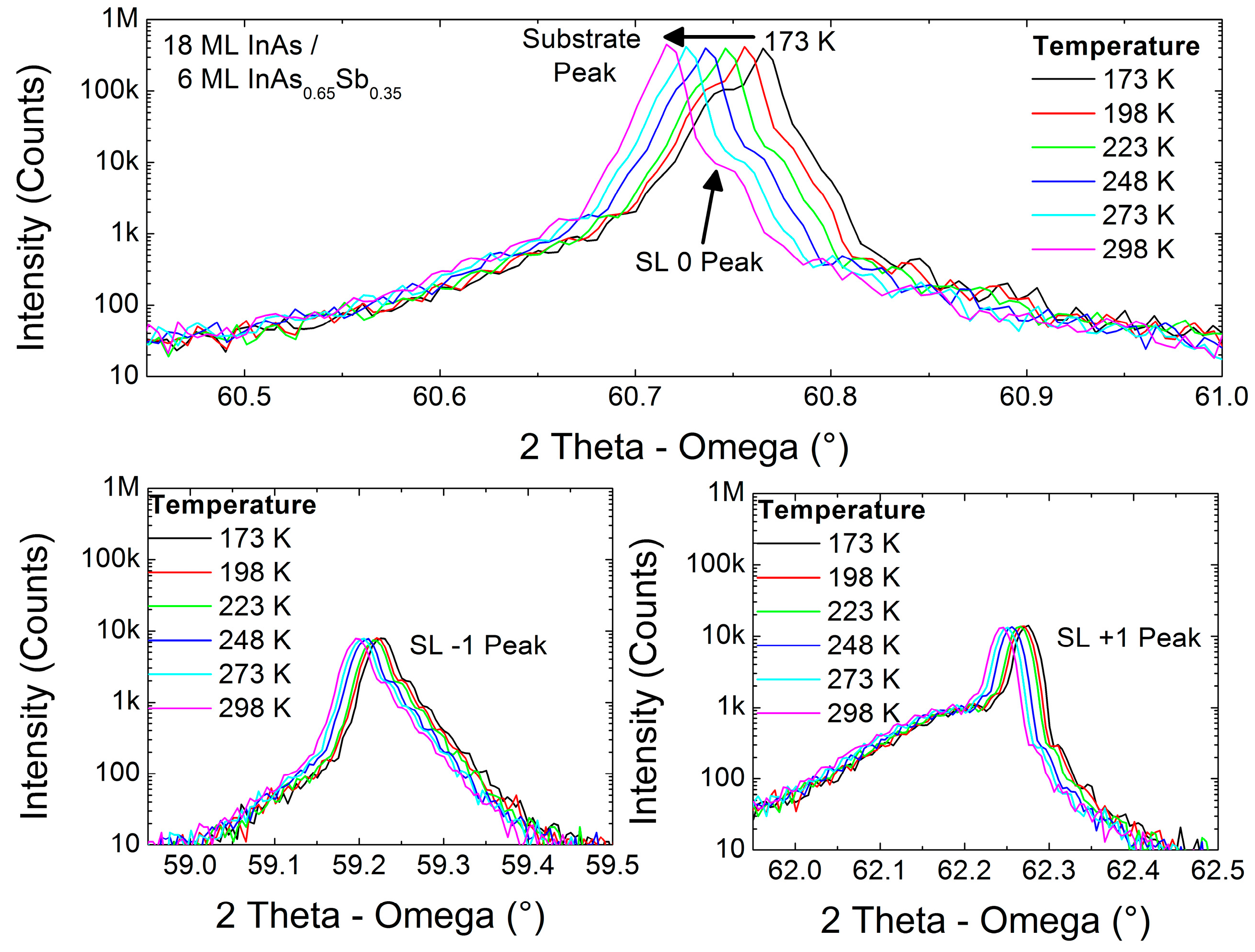
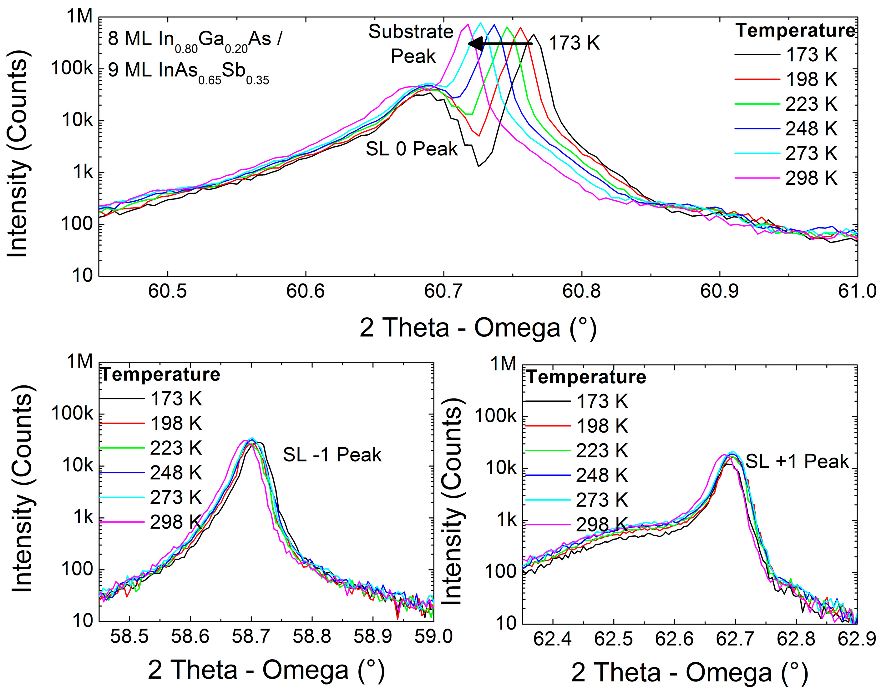
2. Results
3. Discussion
4. Materials and Methods
5. Conclusions
Acknowledgments
Author Contributions
Conflicts of Interest
References
- Steenbergen, E.H.; Connelly, B.C.; Metcalfe, G.D.; Shen, H.; Wraback, M.; Lubyshev, D.; Qiu, Y.; Fastenau, J.M.; Liu, A.W.; Elhamri, S.; et al. Significantly improved minority carrier lifetime observed in a long-wavelength infrared III-V type-II superlattice comprised of InAs/InAsSb. Appl. Phys. Lett. 2011, 99, 251110–251113. [Google Scholar] [CrossRef]
- Hoang, A.M.; Chen, G.; Chevallier, R.; Haddadi, A.; Razeghi, M. High performance photodiodes based on InAs/InAsSb type-II superlattices for very long wavelength infrared detection. Appl. Phys. Lett. 2014, 104. [Google Scholar] [CrossRef]
- Plis, E.A.; Schuler-Sandy, T.; Ramirez, D.A. Dark current reduction in InAs/InAsSb superlattice mid-wave infrared detectors through restoration etch. Electron. Lett. 2015, 51, 2009–2010. [Google Scholar] [CrossRef]
- Klipstein, P.C. XBnn and XBpp infrared detectors. J. Cryst. Growth 2015, 425, 351–356. [Google Scholar] [CrossRef]
- Rhiger, D.R.; Smith, E.P.; Kolasa, B.P.; Kim, J.K.; Klem, J.F.; Hawkins, S.D. Analysis of III–V Superlattice nBn Device Characteristics. J. Electron. Mater. 2016, 45, 4646–4653. [Google Scholar] [CrossRef]
- Olson, B.V.; Kim, J.K.; Kadlec, E.A.; Klem, J.F.; Hawkins, S.D.; Coon, W.T.; Fortune, T.R.; Tauke-Pedretti, A.; Cavaliere, M.A.; Shaner, E.A. Optical and electrical properties of narrow-bandgap infrared W-structure superlattices incorporating AlAs/AlSb/AlAs barrier layers. Appl. Phys. Lett. 2016, 108, 252104. [Google Scholar] [CrossRef]
- Donetsky, D.; Svensson, S.P.; Vorobjev, L.E.; Belenky, G. Carrier lifetime measurements in short-period InAs/GaSb strained-layer superlattice structures. Appl. Phys. Lett. 2009, 95, 212104. [Google Scholar] [CrossRef]
- Ting, D.Z.-Y.; Hill, C.J.; Soibel, A.; Keo, S.A.; Mumolo, J.M.; Nguyen, J.; Gunapala, S.D. A high-performance long wavelength superlattice complementary barrier infrared detector. Appl. Phys. Lett. 2009, 95, 023508. [Google Scholar] [CrossRef]
- Connelly, B.C.; Metcalfe, G.D.; Shen, H.; Wraback, M.; Canedy, C.L.; Vurgaftman, I.; Melinger, J.S.; Affouda, C.A.; Jackson, E.M.; Nolde, J.A.; et al. Investigation of Trap States in Mid-Wavelength Infrared Type II Superlattices Using Time-Resolved Photoluminescence. J. Electron. Mater. 2013, 42, 3203–3210. [Google Scholar] [CrossRef]
- Fuchs, F.; Weimer, U.; Pletschen, W.; Schmitz, J.; Ahlswede, E.; Walther, M.; Wagner, J.; Koidl, P. High performance InAs/Ga1-xInxSb superlattice infrared photodiodes. Appl. Phys. Lett. 1997, 71, 3251–3253. [Google Scholar] [CrossRef]
- Ariyawansa, G.; Reyner, C.J.; Steenbergen, E.H.; Duran, J.M.; Reding, J.D.; Scheihing, J.E.; Bourassa, H.R.; Liang, B.L.; Huffaker, D.L. InGaAs/InAsSb strained layer superlattices for mid-wave infrared detectors. Appl. Phys. Lett. 2016, 108, 022106. [Google Scholar] [CrossRef]
- Canedy, C.L.; Aifer, E.H.; Vurgaftman, I.; Tischler, J.G.; Meyer, J.R.; Warner, J.H.; Jackson, E.M. Antimonide Type-II “W” Photodiodes with Long-Wave Infrared R 0 A Comparable to HgCdTe. J. Electron. Mater. 2007, 36, 852–856. [Google Scholar] [CrossRef]
- Tennant, W.E. “Rule 07” revisited: Still a good heuristic predictor of p/n HgCdTe photodiode performance? J. Electron. Mater. 2010, 39, 1030–1035. [Google Scholar] [CrossRef]
- Ting, D.Z.; Soibel, A.; Gunapala, S.D. Hole effective masses and subband splitting in type-II superlattice infrared detectors. Appl. Phys. Lett. 2016, 108, 183504. [Google Scholar] [CrossRef]
- Ariyawansa, G.; Reyner, C.J.; Duran, J.M.; Reding, J.D.; Scheihing, J.E.; Steenbergen, E.H. Unipolar infrared detectors based on InGaAs/InAsSb ternary superlattices. Appl. Phys. Lett. 2016, 109, 021112. [Google Scholar] [CrossRef]
- Vurgaftman, I.; Meyer, J.R.; Ram-Mohan, L.R. Band parameters for III–V compound semiconductors and their alloys. J. Appl. Phys. 2001, 89, 5815–5875. [Google Scholar] [CrossRef]
- Ekins-Daukes, N.J.; Kawaguchi, K.; Zhang, J. Strain-Balanced Criteria for Multiple Quantum Well Structures and Its Signature in X-ray Rocking Curves. Cryst. Growth Des. 2002, 2, 287–292. [Google Scholar] [CrossRef]
- Timm, R.; Lenz, A.; Eisele, H.; Ivanova, L.; Dähne, M.; Balakrishnan, G.; Huffaker, D.L.; Farrer, I.; Ritchie, D.A. Quantum ring formation and antimony segregation in GaSb/GaAs nanostructures. J. Vacuum Sci. Technol. B Microelectron. Nanometer Struct. 2008, 26, 1492–1503. [Google Scholar] [CrossRef]
- Shapiro, J.N.; Lin, A.; Huffaker, D.L.; Ratsch, C. Potential energy surface of In and Ga adatoms above the (111)A and (110) surfaces of a GaAs nanopillar. Phys. Rev. B 2011, 84, 085322. [Google Scholar] [CrossRef]
- Nilsen, T.A.; Breivik, M.; Myrvågnes, G.; Fimland, B.-O. Thermal expansion of GaSb measured by temperature dependent X-ray diffraction. J. Vacuum Sci. Technol. B 2010, 28, C3I17–C3I20. [Google Scholar] [CrossRef] [Green Version]
- Lumb, M.P.; Vurgaftman, I.; Affouda, C.A.; Meyer, J.R.; Aifer, E.H.; Walters, R.J. Quantum wells and superlattices for III–V photovoltaics and photodetectors. Proc. SPIE 2012, 8471, 84710A. [Google Scholar]
- Adachi, S. Properties of Group-IV, III–V and II–VI Semiconductors; John Wiley & Sons Ltd.: Chichester, UK, 2005. [Google Scholar]
- Proessdorf, A.; Hanke, M.; Jenichen, B.; Braun, W.; Riechert, H. Volmer-Weber growth of AlSb on Si(111). Appl. Phys. Lett. 2013, 102, 041601. [Google Scholar] [CrossRef]
- Jackson, A.W.; Gossard, A.C. Thermal imaging of wafer temperature in MBE using a digital camera. J. Cryst. Growth 2007, 301–302, 105–108. [Google Scholar] [CrossRef]
- Kuech, T.F.; Khandekar, A.A.; Rathi, M.; Mawst, L.J.; Huang, J.Y.T.; Song, X.; Babcock, S.E.; Meyer, J.R.; Vurgaftman, I. MOVPE growth of antimonide-containing alloy materials for long wavelength applications. J. Cryst. Growth 2008, 310, 4826–4830. [Google Scholar] [CrossRef]

© 2016 by the authors; licensee MDPI, Basel, Switzerland. This article is an open access article distributed under the terms and conditions of the Creative Commons Attribution (CC-BY) license (http://creativecommons.org/licenses/by/4.0/).
Share and Cite
Reyner, C.J.; Kiefer, A.M.; Ariyawansa, G.; Duran, J.M.; Scheihing, J.E. Temperature-Dependent X-ray Diffraction Measurements of Infrared Superlattices Grown by MBE. Crystals 2016, 6, 150. https://doi.org/10.3390/cryst6110150
Reyner CJ, Kiefer AM, Ariyawansa G, Duran JM, Scheihing JE. Temperature-Dependent X-ray Diffraction Measurements of Infrared Superlattices Grown by MBE. Crystals. 2016; 6(11):150. https://doi.org/10.3390/cryst6110150
Chicago/Turabian StyleReyner, Charles J., Arnold M. Kiefer, Gamini Ariyawansa, Joshua M. Duran, and John E. Scheihing. 2016. "Temperature-Dependent X-ray Diffraction Measurements of Infrared Superlattices Grown by MBE" Crystals 6, no. 11: 150. https://doi.org/10.3390/cryst6110150