Article

Study of Dislocations in the Minicrystallized Regions in Multicrystalline Silicon Grown by the Directional Solidification Method

1
School of Materials Science and Engineering, Nanchang University, Nanchang 330031, China
2
Department of Science, Nanchang Institute of Technology, Nanchang 330099, China
*
Author to whom correspondence should be addressed.
Crystals 2016, 6(10), 130; https://doi.org/10.3390/cryst6100130
Submission received: 3 September 2016 / Revised: 3 October 2016 / Accepted: 6 October 2016 / Published: 12 October 2016
(This article belongs to the Special Issue Crystal Dislocations)

Abstract

:
Directionally solidified multicrystalline silicon (mc-Si)-based solar cells have dominated the global photovoltaic market in recent years. The photovoltaic performance of mc-Si solar cells is strongly influenced by their crystalline defects. The occurrence of minicrystallization results in much smaller grain size and, therefore, a larger number of grain boundaries in mc-Si ingots. Dislocations in the minicrystallized regions have been rarely investigated in the literature. In this work, optical microscopy was used to investigate dislocations in the mincrystallized regions in mc-Si ingots grown by the directional solidification method. The distribution of dislocations was found to be highly inhomogeneous from one grain to another in the mincrystallized regions. High inhomogeneity of dislocation distribution was also observed in individual grains. Serious shunting behavior was observed in the mc-Si solar cells containing minicrystallized regions, which strongly deteriorates their photovoltaic properties. The shunting was found to be highly localized to the minicrystallized regions.

Graphical Abstract

1. Introduction

Renewable energy technology has been receiving much attention in recent years as a result of severe global warming due to excessive greenhouse gas emission. As one of the most important and advanced renewable energy technologies, the photovoltaic (PV) industry has enjoyed a high growth rate in the last decade [1,2]. At present, solar cells based on crystalline silicon (c-Si), including both multicrystalline (mc) and single crystalline (sc) silicon, dominate the global PV market. Due to the relatively low cost associated with the production of mc-Si ingots, more than half of the c-Si solar cells in the world are based on mc-Si. Production of mc-Si starts with the melting of solar-grade Si feedstock in silica crucibles (coated with Si3N4 on its inner surfaces) in a protected atmosphere of argon. The molten Si is then directionally solidified to form an mc-Si ingot. The weight of an industrial mc-Si ingot for mc-Si solar cells is generally over 500 kg. Wafers with a cross-section area of 156 mm × 156 mm and a thickness about 180~200 μm are obtained using the wire sawing process.
Crystalline defects—such as grain boundaries [3] and dislocations [4,5,6,7,8,9,10,11,12,13,14,15,16,17,18,19]—impurities [20,21], and foreign inclusions [22,23,24] in mc-Si wafers degrade the PV performance of mc-Si solar cells. In order to enhance the PV performance of mc-Si solar cells, a lot of effort has been devoted to reducing the number of grain boundaries and the dislocation densities in mc-Si [7,25,26]. However, the occurrence of minicrystallization [27] in mc-Si ingots that are grown by the directional solidification method introduces much smaller grains within the minicrystallized regions (Figure 1), resulting in a larger number of grain boundaries within these regions, which can degrade the PV performance of mc-Si solar cells.
Up to now, little research has been reported on the dislocation characteristics in the minicrystallized regions in mc-Si ingots grown by the directional solidification method. In this work, the dislocation characteristics in the minicrystallized regions were studied using optical microscopy. The PV properties of mc-Si solar cells containing minicrystallized regions were investigated.

2. Experiment

Mc-Si ingots were grown by a local PV mc-Si wafer manufacturer using an industrial directional solidification system (DSS, GT Solar). These mc-Si ingots were generally over 500 kg in weight. The mc-Si ingots are boron-doped and have a resistivity of about 1.0–2.5 Ω cm. In this work, mc-Si ingots (intended for commercial mc-Si solar cells) containing minicrystallized regions were selected for sample preparation in this study. After the surfaces of these mc-Si samples containing minicrystallized regions were polished, two steps of an etching process—a Secco solution used for the first step followed by a Yang solution etching—were conducted to reveal dislocation etch pits. An optical microscope (VHX 600) was employed to observe the dislocations in the mc-Si samples containing minicrystallized regions.
Mc-Si wafers (156 mm × 156 mm) with or without minicrystallized regions were selected for fabricating solar cells under identical processing conditions. The mc-Si solar cells in this work were manufactured by the standard PV industry manufacturing line [28]. In brief, mc-Si wafers were textured for light trapping, followed by phosphorous diffusion. Phosphosilicate glass (PSG) was removed by diluted hydrofluoric acid (HF) solution. The parasitic pn junctions at the wafer edge and rear were etched off using mixed acid solution. The emitter sheet resistance was about 60 Ω/□. SiNx:H antireflection coatings were deposited on the front surfaces by plasma-enhanced chemical vapor deposition (PECVD, Centrotherm, excitation frequency at 40 kHz). Aluminium and silver pastes were screen-printed on the rear and front surfaces of the mc-Si wafers, respectively. After drying, the metallized mc-Si wafers were then sintered in a belt furnace to form the front and back electrodes as well as the back-surface field (BSF). The PV properties of the solar cells were characterized at room temperature under the air mass (AM) 1.5G illumination.

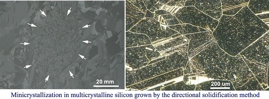
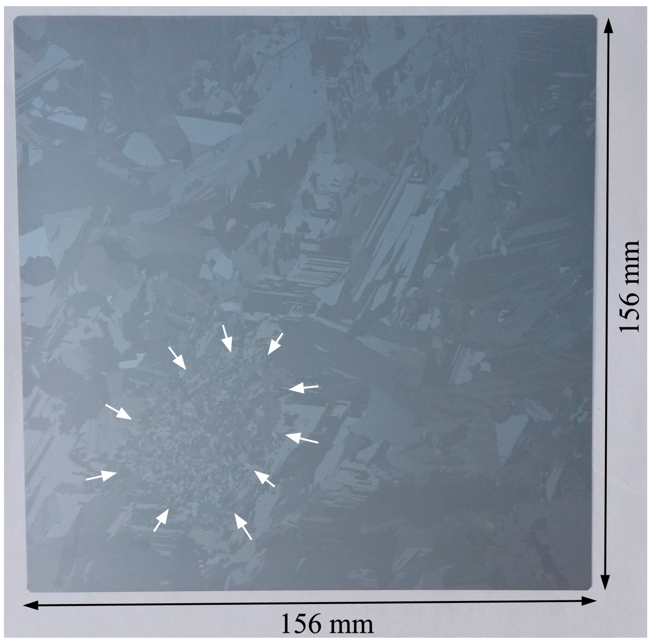
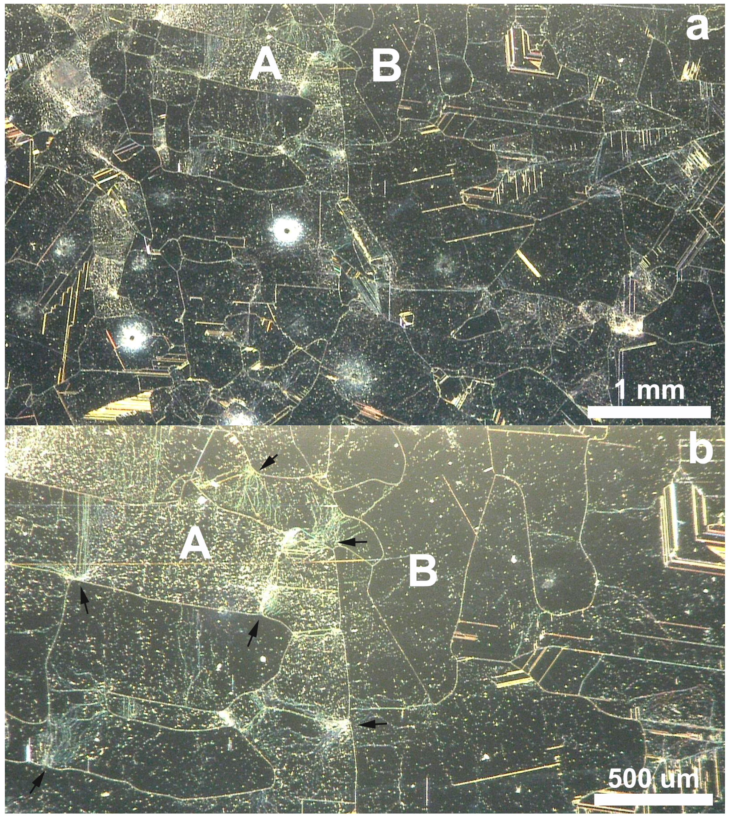
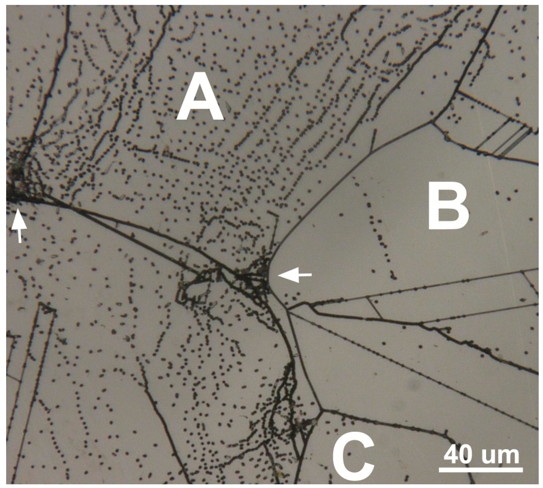
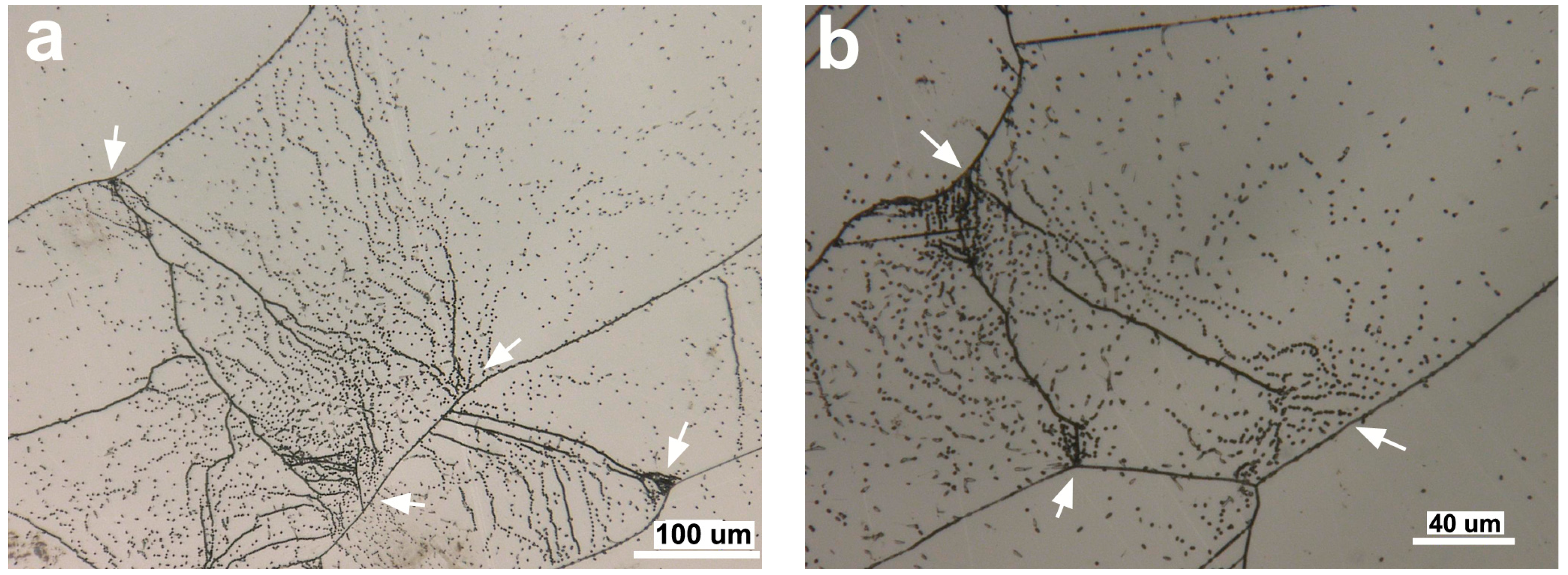
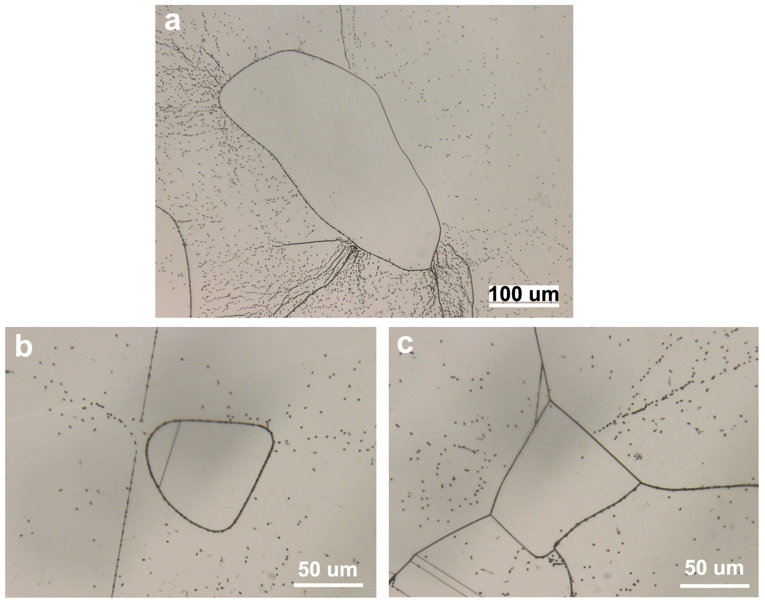
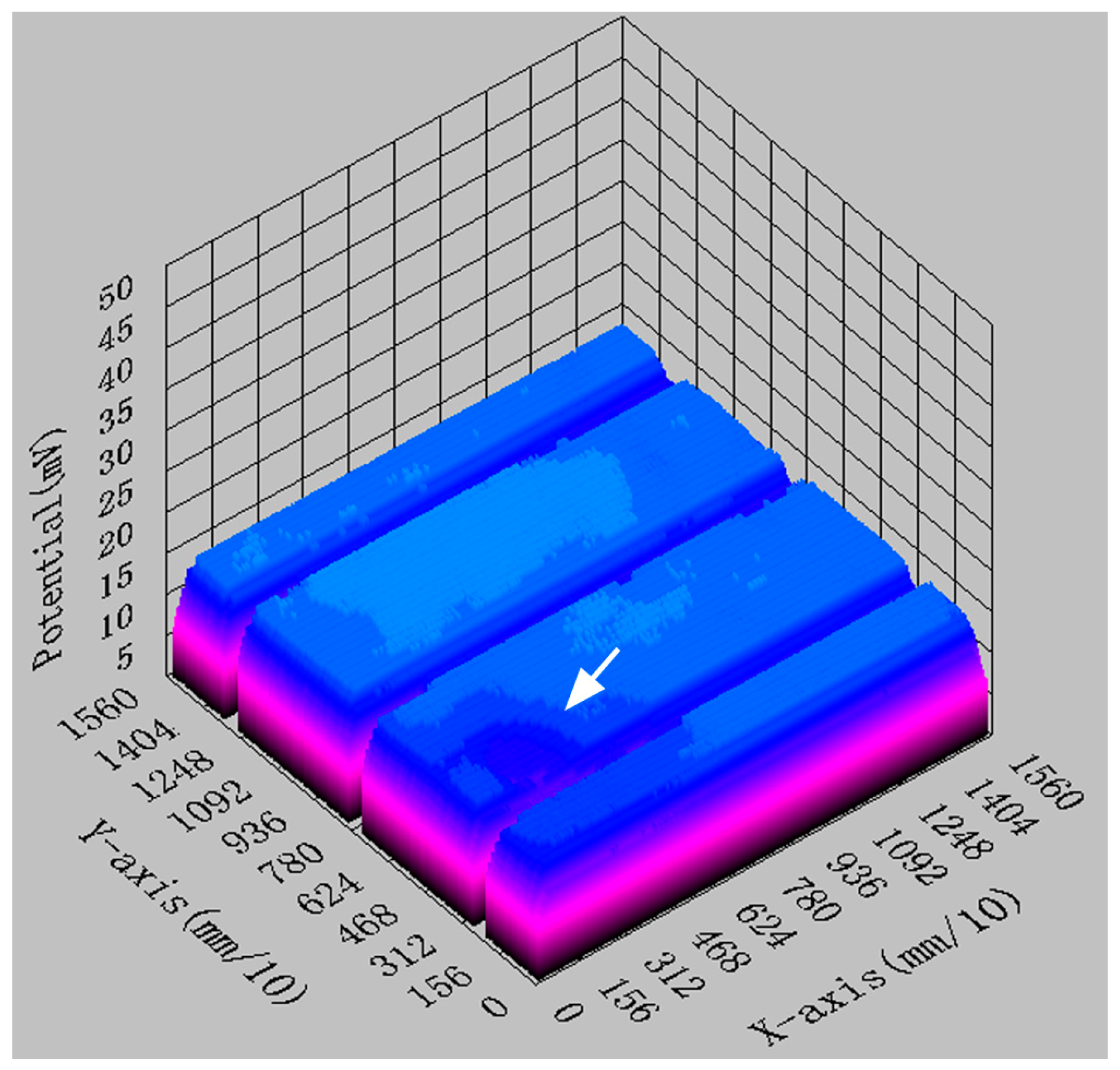
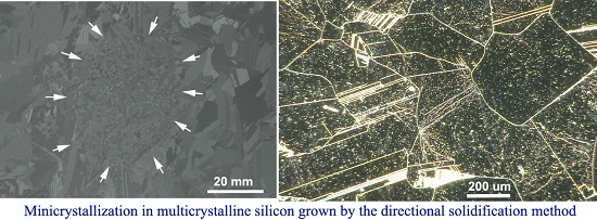
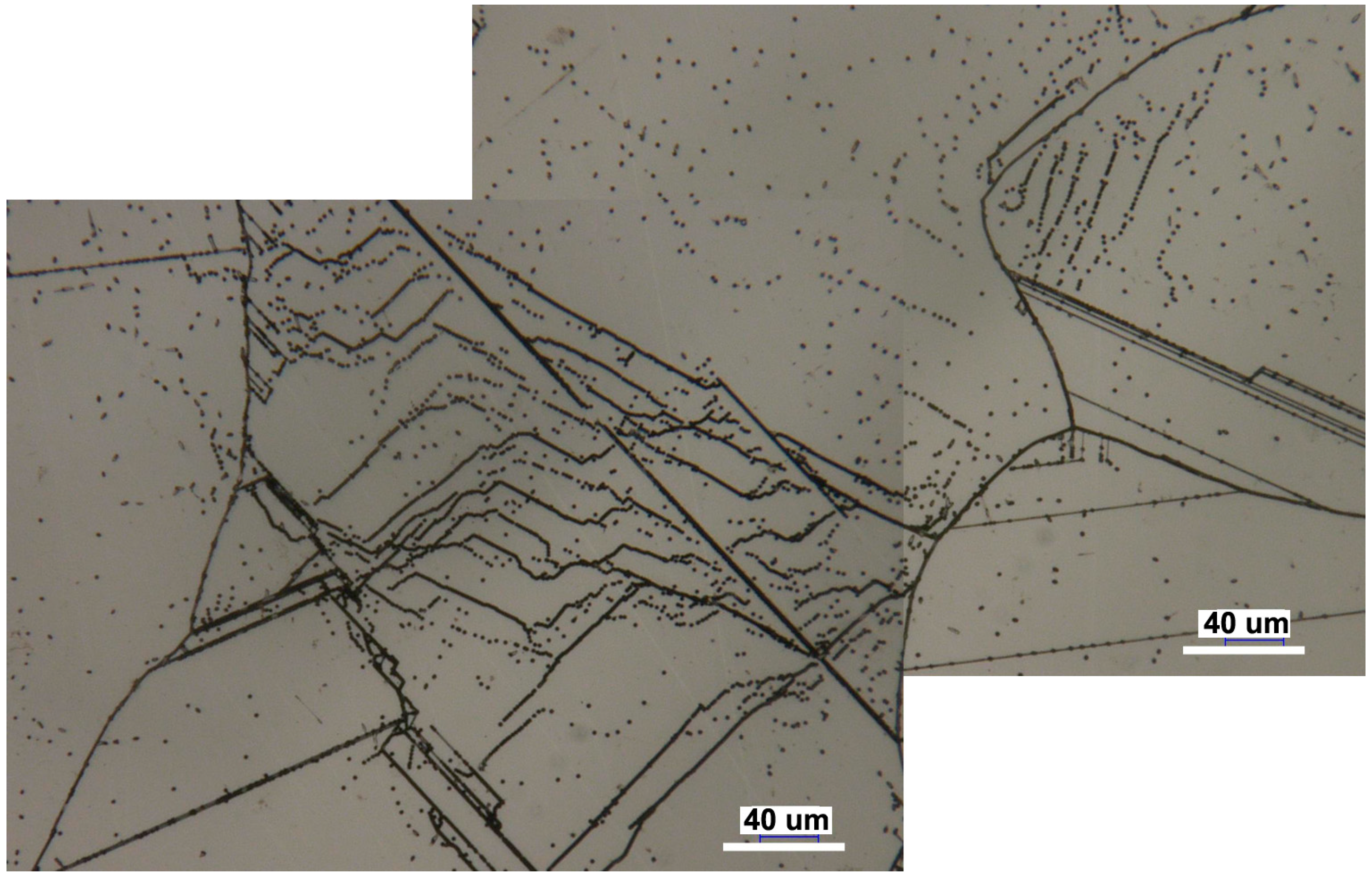
3. Results and Discussion

Figure 2 shows the optical microscopy images for a minicrystallized region in the mc-Si sample grown by the directional solidification method. The distribution of dislocations is highly inhomogeneous among grains in the minicrystallized region. For instance, as shown in Figure 2, grain A has a much higher dislocation density than grain B. Such a highly inhomogeneous distribution of dislocations among grains was also observed in the normal regions of mc-Si samples [19]. This high inhomogeneity of dislocation distribution can be better observed among grains A, B, and C in Figure 3, which was captured at a higher magnification. In Figure 3, the average dislocation density in grains A, B, and C is estimated to be about 9.8 × 106 cm−2, 2.6 × 105 cm−2, and 2.5 × 105 cm−2, respectively. This represents a difference of about 39 times in their dislocation density between grain A and grain C. In addition, the dislocation distribution is also rather inhomogeneous within individual grains. For instance, in grain A, as indicated by the white arrows in Figure 3, two densely distributed dislocation clusters are present, and their dislocation density is over 1 × 108 cm−2.
As indicated by black arrows in Figure 2b, some dense dislocation clusters emanate from the grain boundaries. In Figure 4 with higher magnification, as indicated by the white arrows, this phenomenon can be better observed. This suggests that grain boundaries can be one of the dislocation generation sources. These dislocations are mostly slip dislocations, and they should be generated during the solidification stage due to the thermal stress originating from the neighboring grains [19].
Some small grains in the minicrystallized regions are free of dislocations, while others contain only a rather small number of dislocations. As shown in Figure 5a, only about 10 dislocations can be observed in the central grain. No dislocation is present in the central grain in Figure 5b, and only 3 dislocations are observed in the central grain in Figure 5c. It is noted in Figure 5a,b that each of the two grains is embedded within a larger grain. For the occurrence of such grains that are free of dislocation or containing rather few dislocations, one possible cause is that they originally contained slip dislocations (Figure 6), which could actively move and merge to form grain boundaries during the solidification cooling stage when the temperature is still high. Slip dislocation is an array of dislocation, which in fact can be considered as a low-angle grain boundary [29]. When two arrays of moving slip dislocations meet, they form a new low-angle grain boundary, which has a higher misorientation angle than the previous one. When more arrays of moving slip dislocations join the above two, the misorientation angle of the grain boundary will become higher. Consequently, a new grain with rather low density of dislocations is formed (Figure 5a,b). Nevertheless, the situation for the small grain containing rather few dislocations in Figure 5c is different from these two grains in Figure 5a,b, both of which are embedded in a single grain. It can be seen in Figure 5c that it is located in the junction region of four larger grains. One possible cause for the formation of the small grain containing rather few dislocations in Figure 5c could be a result of recrystallization during the solidification cooling stage when the temperature is still high. Further research will be needed in order to understand the underlying mechanism for the dislocation-free grains and the grain with very low dislocation density.
In order to study the influence of minicrystallization on the PV properties of mc-Si solar cells, two mc-Si wafers (156 mm × 156 mm) were processed into solar cells. One wafer contained a minicrystallized region (Figure 1), while the other was a normal wafer, free of minicrystallization. Table 1 shows the PV properties (open circuit voltage Voc, short circuit current Isc, series resistance Rs, shunt resistance Rsh, fill factor FF, and conversion efficiency η) of the two mc-Si solar cells with and without minicrystallization. Rs and Rsh were determined from the illuminated current–voltage (I–V) curves.
As expected, the mc-Si solar cell free of minicrystallization had a much higher conversion efficiency (η = 16.87%) than the one containing minicrystallization (η = 9.59%). It is interesting to note in Table 1 that Isc of the mc-Si solar cell with minicrystallization was 8.87 A, which is greater than the cell free of minicrystallization (Isc = 8.40 A). However, Voc of the mc-Si solar cell with minicrystallization was 596.2 mV, which is smaller than the cell free of minicrystallization (Voc = 622.4 mV). Thus, Voc and Isc of the two solar cells are different, but their difference is only about 6%. However, the two cells had rather different FF values; FF = 45.25% for the one with minicrystallization and FF = 78.51% for the one without minicrystallization. This large difference in their FF values explains their rather different conversion efficiencies (Table 1). The reason for the much lower FF value for the cell with minicrystallization is because it had a much smaller shunt resistance Rsh [30]. As shown in Table 1, the cell with minicrystallization had Rsh = 0.20 Ω, while the cell free of minicrystallization had Rsh = 149.59 Ω. This indicates that the occurrence of minicrystallization results in a very strong shunting behavior in the mc-Si solar cell. The shunting behavior in the mc-Si solar cell with minicrystallization can be directly viewed in the mapping graph recorded using a Corescan scanner (Figure 7). As indicated by the white arrow in Figure 7, it can be clearly seen that the shunting was highly localized in the minicrystallized region. Some researchers [24] reported that SiC filaments are observed within the grain boundaries of mc-Si grown by the directional solidification method, and the SiC filaments are believed to be responsible for shunting behaviors in mc-Si solar cells. However, no SiC was observed in the minicrystallized region in this work, and this could be because Si feedstock with low carbon concentration was used in this work. The major cause for the severe shunting behavior in the minicrystallized region should be the highly inhomogeneously distributed dislocations and the large number of grain boundaries in this region. It has been shown [31] that the high strain within the dislocation core can cause local distortion of the band structure and result in the formation of a quantum well. This may help explain the occurrence of the local shunting within the minicrystallized region. Nevertheless, further studies will be needed in order to fully understand the underlying mechanism of such localized shunting behavior.

4. Conclusions

Optical microscopy was employed to investigate dislocations in the minicrystallized regions in mc-Si ingots grown by the directional solidification method. The distribution of dislocations was found to be highly inhomogeneous from one grain to another in the mincrystallized regions. Some grains can be free of dislocations, while others can have a dislocation density in the magnitude from 106 cm−2 to 108 cm−2. In addition, high inhomogeneity of dislocation distribution was also observed in individual grains. Serious shunting behavior was observed in the mc-Si solar cells, which contained minicrystallized regions, and it strongly deteriorated their photovoltaic properties. The shunting was found to be highly localized to the minicrystallized regions.

Acknowledgments

This work was supported by the National Natural Science Foundation of China (number 51362020).

Author Contributions

Nan Chen and Guoping Du conceived and designed the experiments; Nan Chen, Shenyu Qiu, Jianhua Huang and Guihua Liu performed the experiments; Nan Chen and Guoping Du analyzed the data and wrote the paper.

Conflicts of Interest

The authors declare no conflict of interest.

References

  1. Swanson, R.M. A vision for crystalline silicon photovoltaics. Prog. Photovolt. Res. Appl. 2006, 14, 443–453. [Google Scholar] [CrossRef]
  2. Budhraja, V.; Misra, D.; Ravindra, N.M. Advancements in PV multicrystalline silicon solar cells from 1980 to 2010—An overview. In Proceedings of the 37th IEEE Photovoltaic Specialists Conference, Seattle, WA, USA, 19–24 June 2011.
  3. Schumann, M.; Haas, T.; Orellana Pérez, T.; Riepe, S. Grain size distribution in multicrystalline silicon for structure characterization of silicon wafers. In Proceedings of the 26th European PV Solar Energy Conference and Exhibition, Hamburg, Germany, 2–9 September 2011.
  4. El Ghitani, H.; Pasquinelli, M.; Martinuzzi, S. Influence of dislocations on photovoltaic properties of multicrystalline silicon solar cells. J. Phys. III 1993, 3, 1941–1946. [Google Scholar] [CrossRef]
  5. Schindler, R.; Räuber, A. Defects in multicrystalline silicon. Solid State Phenom. 1991, 19–20, 341–352. [Google Scholar] [CrossRef]
  6. Sopori, B. Impurities and defects in photovoltaic Si devices: A review. In Proceedings of the 10th International Workshop on the Physics of Semiconductor Devices, Delhi, India, 14–18 December 1999.
  7. Hartman, K.; Bertoni, M.; Serdy, J.; Buonassisi, T. Dislocation density reduction in multicrystalline silicon solar cell material by high temperature annealing. Appl. Phys. Lett. 2008, 93, 122108. [Google Scholar] [CrossRef]
  8. Ryningen, B.; Stokkan, G.; Kivambe, M.; Ervik, T.; Lohne, O. Growth of dislocation clusters during directional solidification of multicrystalline silicon ingots. Acta Mater. 2011, 59, 7703–7710. [Google Scholar] [CrossRef]
  9. Stokkan, G.; Riepe, S.; Lohne, O.; Warta, W. Spatially resolved modeling of the combined effect of dislocations and grain boundaries on minority carrier lifetime in multicrystalline silicon. J. Appl. Phys. 2007, 101, 053515. [Google Scholar] [CrossRef]
  10. Fathi, M.; Bouhafs, D. A new detection technique of crystalline defects by sheet resistance measurement on multicrystalline silicon wafers. Semicond. Sci. Technol. 2006, 21, 437–442. [Google Scholar] [CrossRef]
  11. Kim, D.I.; Kim, Y.K. Characteristics of structural defects in the 240 kg silicon ingot grown by directional solidification process. Sol. Energy Mater. Sol. Cells 2006, 90, 1666–1672. [Google Scholar] [CrossRef]
  12. Istratov, A.A.; Hieslmair, H.; Vyvenko, O.F.; Weber, E.R.; Schindler, R. Defect recognition and impurity detection techniques in crystalline silicon for solar cells. Sol. Energy Mater. Sol. Cells 2002, 72, 441–451. [Google Scholar] [CrossRef]
  13. Luque, A.; Hegedus, S. Handbook of Photovoltaic Science and Engineering; John Wiley & Sons Ltd.: West Sussex, UK, 2003. [Google Scholar]
  14. El Ghitani, H.; Martinuzzi, S. Influence of dislocations on electrical properties of large grained polycrystalline silicon cells. I. Model. J. Appl. Phys. 1989, 66, 1717–1722. [Google Scholar] [CrossRef]
  15. Sopori, B.; Chen, W. Influence of distributed defects on the photoelectric characteristics of a large-area device. J. Cryst. Growth 2000, 210, 375–378. [Google Scholar] [CrossRef]
  16. Donolato, C. Modeling the effect of dislocations on the minority carrier diffusion length of a semiconductor. J. Appl. Phys. 1998, 84, 2656–2664. [Google Scholar] [CrossRef]
  17. Takahashi, I.; Usami, N.; Kutsukake, K.; Stokkan, G.; Morishita, K.; Nakajima, K. Generation mechanism of dislocations during directional solidification of multicrystalline silicon using artificially designed seed. J. Cryst. Growth 2010, 312, 897–901. [Google Scholar] [CrossRef]
  18. Choi, H.; Bertoni, M.; Hofstetter, J.; Fenning, D.; Powell, D.; Castellanos, S.; Buonassisi, T. Dislocation density reduction during impurity gettering in multicrystalline silicon. IEEE J. Photovolt. 2013, 3, 189–198. [Google Scholar] [CrossRef]
  19. Chen, N.; Qiu, S.; Liu, B.; Du, G.; Liu, G.; Sun, W. An optical microscopy study of dislocations in multicrystalline silicon grown by directional solidification method. Mater. Sci. Semicond. Process. 2010, 13, 276–280. [Google Scholar] [CrossRef]
  20. Isenberg, J.; Dicker, J.; Warta, W. Averaging of laterally inhomogeneous lifetimes for one-dimensional modeling of solar cells. J. Appl. Phys. 2003, 94, 4122–4130. [Google Scholar] [CrossRef]
  21. Kieliba, T.; Riepe, S.; Warta, W. Effect of dislocations on open circuit voltage in crystalline silicon solar cells. J. Appl. Phys. 2006, 100, 093708. [Google Scholar] [CrossRef]
  22. Chen, N.; Liu, B.; Qiu, S.; Liu, G.; Du, G. Study of SiC and Si3N4 inclusions in industrial multicrystalline silicon ingots grown by directional solidification method. Mater. Sci. Semicond. Process. 2010, 13, 231–238. [Google Scholar] [CrossRef]
  23. Søiland, A.K.; Ørelid, E.J.; Engh, T.A.; Lohne, O.; Tuset, J.K.; Gjerstad, Ø. SiC and Si3N4 inclusions in multicrystalline silicon ingots. Mater. Sci. Semicond. Process. 2004, 7, 39–43. [Google Scholar] [CrossRef]
  24. Lotnyk, A.; Bauer, J.; Breitenstein, O.; Blumtritt, H. A TEM study of SiC particles and filaments precipitated in multicrystalline Si for solar cells. Sol. Energy Mater. Sol. Cells 2008, 92, 1236–1240. [Google Scholar] [CrossRef]
  25. Yang, Y.M.; Yu, A.; Hsu, B.; Hsu, W.C.; Yang, A.; Lan, C.W. Development of high-performance multicrystalline silicon for photovoltaic industry. Prog. Photovolt. Res. Appl. 2015, 23, 340–351. [Google Scholar] [CrossRef]
  26. Fujiwara, K.; Pan, W.; Sawada, K.; Tokairin, M.; Usami, N.; Nose, Y.; Nomura, A.; Shishido, T.; Nakajima, K. Directional growth method to obtain high quality polycrystalline silicon from its melt. J. Cryst. Growth 2006, 292, 282–285. [Google Scholar] [CrossRef]
  27. Liu, B.; Chen, N.; Du, G.; Liu, G.; Li, Y.; Sun, W.; Rossetto, P. Minicrystallization in directionally solidified multicrystalline silicon and its effect on the photovoltaic properties of solar cells. Phys. Status Solidi A 2011, 208, 2478–2481. [Google Scholar] [CrossRef]
  28. Du, G.; Zhang, Y.; Li, W.; Chen, N.; Liu, B.; Sun, J. Performance enhancement of multicrystalline silicon solar cells and modules using double-layered SiNx:H antireflection coatings. Prog. Photovolt. Res. Appl. 2015, 23, 1806–1814. [Google Scholar] [CrossRef]
  29. Chadwick, G.A.; Smith, D.A. Grain Boundary Structure and Properties; Academic Press Inc.: New York, NY, USA, 1976. [Google Scholar]
  30. Wenham, S.R.; Green, M.A.; Watt, M.E.; Corkish, R. Applied Photovoltaics, 2nd ed.; Earthscan: London, UK, 2007. [Google Scholar]
  31. Reiche, M.; Kittler, M. Electronic and optical properties of dislocations in silicon. Crystals 2016, 6, 74. [Google Scholar] [CrossRef]
Figure 1. Photograph of a multicrystalline silicon (mc-Si) wafer (156 mm × 156 mm) containing a minicrystallized region (indicated by the white arrows).
Crystals 06 00130 g001
Figure 2. Optical microscopy images of the minicrystallized region with relatively low (a) and high (b) magnification. The bar length is 1 mm for (a) and 500 μm for (b).
Crystals 06 00130 g002
Figure 3. Image of grains with different dislocation densities from one grain to another.
Crystals 06 00130 g003
Figure 4. Image of grains with dislocations emanating from grain boundaries: (a) with four regions, and (b) with three regions.
Crystals 06 00130 g004
Figure 5. Image of grains containing few dislocations or free of dislocations: (a) and (b) embedded within a larger grain, and (c) located at the junction of four larger grains.
Crystals 06 00130 g005
Figure 6. Image of slip dislocations in the minicrystallized regions. Two images were combined in this image to show a larger region.
Crystals 06 00130 g006
Figure 7. Image of shunting behavior of the mc-Si solar cell containing a minicrystallized region.
Crystals 06 00130 g007
Table 1. Photovoltaic (PV) properties of the two mc-Si solar cells with and without minicrystallization.
Solar CellMinicrystallizationVoc (mV)Isc (A)Rs (Ω)Rsh (Ω)FF (%)η (%)
1Yes596.28.870.0010.2045.259.59
2No622.48.400.003149.5978.5116.87

