Article

Numerical and Experimental Study of Optoelectronic Trapping on Iron-Doped Lithium Niobate Substrate

1
Department of Electrical, Computer and Biomedical Engineering, University of Pavia, Via Ferrata 5A, 27100 Pavia, Italy
2
Physics and Astronomy Department, University of Padua, via Marzolo 8, 35131 Padova, Italy
3
Currently at Institute of Applied Physics, University of Bern, Sidlerstrasse 5, CH-3012 Bern, Switzerland
4
Currently at Department of Biomedical Science and Translational Medicine, Università di Milano, Via Vanvitelli 32, 20133 Milano, Italy
*
Author to whom correspondence should be addressed.
Crystals 2016, 6(10), 123; https://doi.org/10.3390/cryst6100123
Submission received: 19 July 2016 / Revised: 16 August 2016 / Accepted: 2 September 2016 / Published: 23 September 2016
(This article belongs to the Special Issue Lithium Niobate Crystals)

Abstract

:
Optoelectronic tweezers (OET) are a promising technique for the realization of reconfigurable systems suitable to trap and manipulate microparticles. In particular, dielectrophoretic (DEP) forces produced by OET represent a valid alternative to micro-fabricated metal electrodes, as strong and spatially reconfigurable electrical fields can be induced in a photoconductive layer by means of light-driven phenomena. In this paper we report, and compare with the experimental data, the results obtained by analyzing the spatial configurations of the DEP-forces produced by a 532 nm laser beam, with Gaussian intensity distribution, impinging on a Fe-doped Lithium Niobate substrate. Furthermore, we also present a promising preliminary result for water-droplets trapping, which could open the way to the application of this technique to biological samples manipulation.

1. Introduction

Particle manipulation techniques are fundamental in many research fields, from biology to chemistry or electrical engineering. Among the many solutions that can be found in literature to achieve this target, optically induced micromanipulation is very promising as it allows contactless trapping and gentle movement of objects, a key feature in biology, where cell viability is crucial. The first works on optical micromanipulation appeared in literature about 40 years ago with the idea of optical tweezers [1,2,3], which exploit optical forces induced by laser sources to handle microparticles. Nowadays, many examples of lab-on-chip devices enabling particle trapping and manipulation can be found in the scientific literature with applications in the fields of biology and pharmacology [4,5,6,7]. Moreover, in the last few years, Stokes trapping has been developed to provide a purely hydrodynamic trapping method, allowing for particle manipulation in solution without need of optical, electric, acoustic, or magnetic fields [8].
Those techniques are however generally best suited for single-particle manipulation, whereas many applications, would greatly benefit from the realization of arrays of traps for multiple-particles parallel manipulation. For this reason, in recent years, the possibility to trap and handle objects with electrophoretic and dielectrophoretic (DEP) forces was investigated [9]. In particular DEP forces, generally produced by an electric field (E-field in the following) gradient, created as an example by means of micro-fabricated metal electrodes, attracted a significant interest as they can also be applied to non-charged particles. At the state of art, a promising alternative is offered by optoelectronic tweezers (OET), in which high-intensity E-fields can be achieved thanks to the use of a photoconductive layer, allowing to obtain strong and reconfigurable traps [10,11].
Lithium Niobate (LiNbO3) is an extremely promising material for such applications due to its large availability, its high optical quality and to the possibility to produce large and localized E-fields by exploiting the internal polarization of the material and the photovoltaic current [12,13,14].
Photorefractive properties of LiNbO3 have been extensively studied in the past [15,16,17], as they have a large impact on many applications of this material, especially those related to the fields of optical communications, optical nonlinear effects, and optical memories. The trapping of dielectric particles and droplets on the surface of x-cut or z-cut LiNbO3 crystals using a low-power spatially-modulated green laser was successfully demonstrated a few years ago in iron doped crystals (Fe:LiNbO3) [17,18,19]. By exploiting the photorefractive properties of the substrate, which can be enhanced by doping the LiNbO3 crystal matrix with few ppm of iron, it is possible to significantly increase the space-charge field in LiNbO3 samples with a low light intensity [20,21]; additionally, by tuning the reduction/oxidation degree of the Fe-ion, it is also possible to control the photorefractive effect response-time [18,22,23].
At the state of the art, few papers report numerical simulation and/or experimental results of DEP in Lithium Niobate [24,25,26,27,28,29,30]. In particular theoretical models and numerical results of photorefractivity-induced trapping (an important tool for the evaluation of DEP forces and their spatial distribution) are presented in references [24,25] and [28], while experimental data are reported in reference [26,27]. Additionally, pyroelectricity-induced trapping of water droplets is described in reference [29,30]. The aim of this manuscript is to develop a numerical model to describe the complete phenomenon and to be able to clarify the processes involved when DEP forces are applied on dielectric particles deposited on a bulk-doped Fe:LiNbO3 sample immersed in water. Several discussions are present in the literature concerning biological applications of this technology, but trapping in water has never been demonstrated. Here we clarify that trapping in water is completely hindered by the role of the charges present even in highly purified water and we present an alternative approach that could open a new scenario for LiNbO3 DEP devices. Moreover, the obtained results provide a useful tool for the design and the optimization of OET in real applications, making it possible to determine the physical parameters that impact on the DEP force strength and distribution. Starting from the intensity-profile of a laser beam used to illuminate the photoconductive substrate, we show a simple process allowing us to evaluate the force field and hence the effectiveness of the trapping regions. The numerical results are validated by comparing the numerical predictions with the experimental results obtained by using PMMA (Poly-methyl-methacrylate) spheres in paraffin oil and Milli-Q water suspension, and water micro-droplets in paraffin oil.

2. Results

In the following, the basic concepts and formulas used to build the simulation will be first shown (Subsection 2.1), then the numerical simulation results will be presented (Subsection 2.2).
In Section 3, the simulations results will be compared with the experimental observations. The description of the experimental setup and the material properties are reported in Section 4.

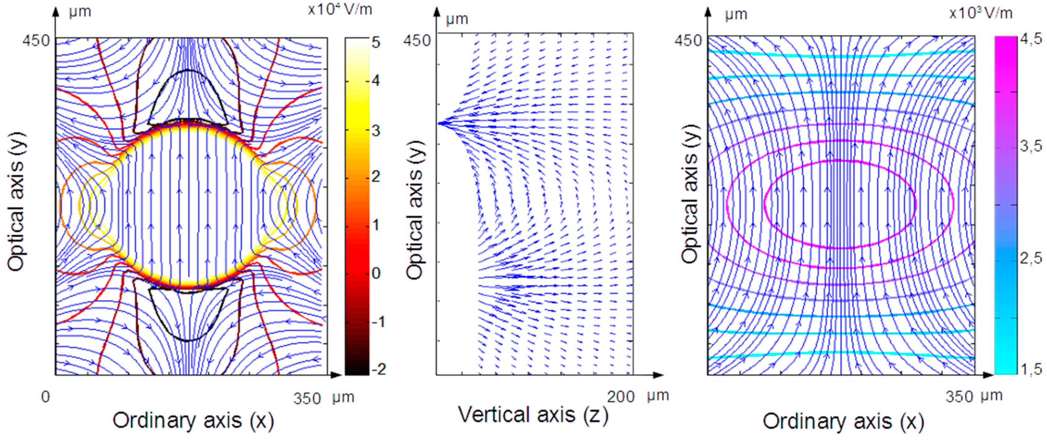
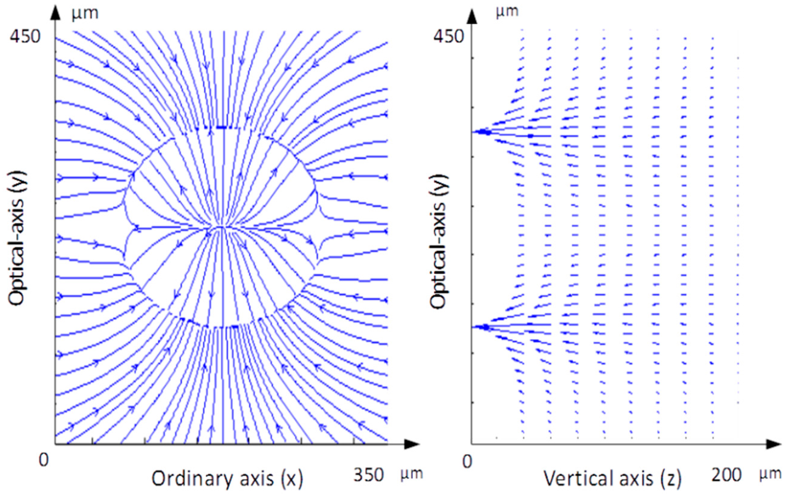
2.1. Photorefractive Field and DEP Force in Lithium Niobate

It is well known that a non-uniform static electric field produces a DEP force FDEP on neutral homogeneous spherical particles (of radius r and dielectric constant ɛp) immersed in a lossless dielectric fluid (dielectric constant ɛm) given by the following equation [31]:
F D E P = 2 π ε m r 3 K E 0 2 ,   K = ( ε p ε m ε p + 2 ε m )
The force depends on the particle volume and on the gradient of the E-field intensity; in general, this is not parallel to the electric field vector E0(r). The force sign, indicating its repulsive or attractive nature, depends on the Clausius-Mossotti factor (K). When the particle permittivity (ɛp) is greater than that of the surrounding medium (ɛm) the force is attractive, and the particle can be trapped in the position where the E-field is maximum, while the force becomes repulsive in the opposite case. The choice of the materials involved in experiments is thus crucial to create a DEP trap, i.e., a position in space characterized by the fact that a “restoring force” brings “escaping particles” back towards the trap point. In our simulations we assume that the space-charge field has reached saturation before depositing the particles on the crystal surface, this allows us to consider the E-field as static (DC), and hence to use the static permittivity value.
The space-charge E-field, originated by the photovoltaic effect, which arises in a Fe:LiNbO3 substrate when it is illuminated by light in the visible range, is the source of the DEP forces in this configuration [18]. We consider the crystal photorefractivity with the so called “single center trap” approach (that is we are considering one single type of free charge carrier and a single impurity center [14]), which is a good approximation under our light intensity condition. Under these hypotheses the field can be calculated by numerically solving the Kukhtarev equation [32,33], where I is the spatial distribution of the laser beam intensity (defined as a function of x and y coordinates for a beam propagating in the z direction: I = I(x,y)), IB is the “background” light-intensity that is introduced in the model to take into account the free carriers thermal generation and e is the electron charge:
[   ( I B   + I ) E + k B T e ( I B + I ) ] = 0
Such an equation can be solved for a LiNbO3 sample (having εo = 84.1, εe = 28.1, Iβ = 1 W/m2) with dimensions Lx and Ly thanks to the boundary conditions for the potential V(x,y) since V = ∇E, considering in this case x and z as ordinary axes and y as the optical axis of the crystal:
V ( x , y = ± L y 2 ) = V B O                                                                                                                     L x 2 < x < + L x 2
V ( x = ± L x 2 , y ) = ( V p h L y ) ( y + L y 2 ) + V B O                                             L y 2 < y < + L y 2
where VBO is a bias voltage (not impacting on the ESC calculation [24]) and Vph is the photovoltaic voltage ideally applied at the border of the crystal along the direction of the optical.
By solving Equation (2), the space-charge field produced in LiNbO3 by laser illumination can be calculated [34]. The charge-distribution created in the region illuminated by the laser beam is the sum of several contributions: diffusion, photovoltaic and drift current [35], which in our case is negligible due to the absence of an external electric field. Additionally, in our case also the diffusion process plays only a minor contribution, given the relatively large size of the beam spot. As it will be explained in the next paragraph the photovoltaic contribution is included in the numerical model as a “bias potential” Vph, which was set to match the standard photovoltaic field of a Fe:LiNbO3 sample.

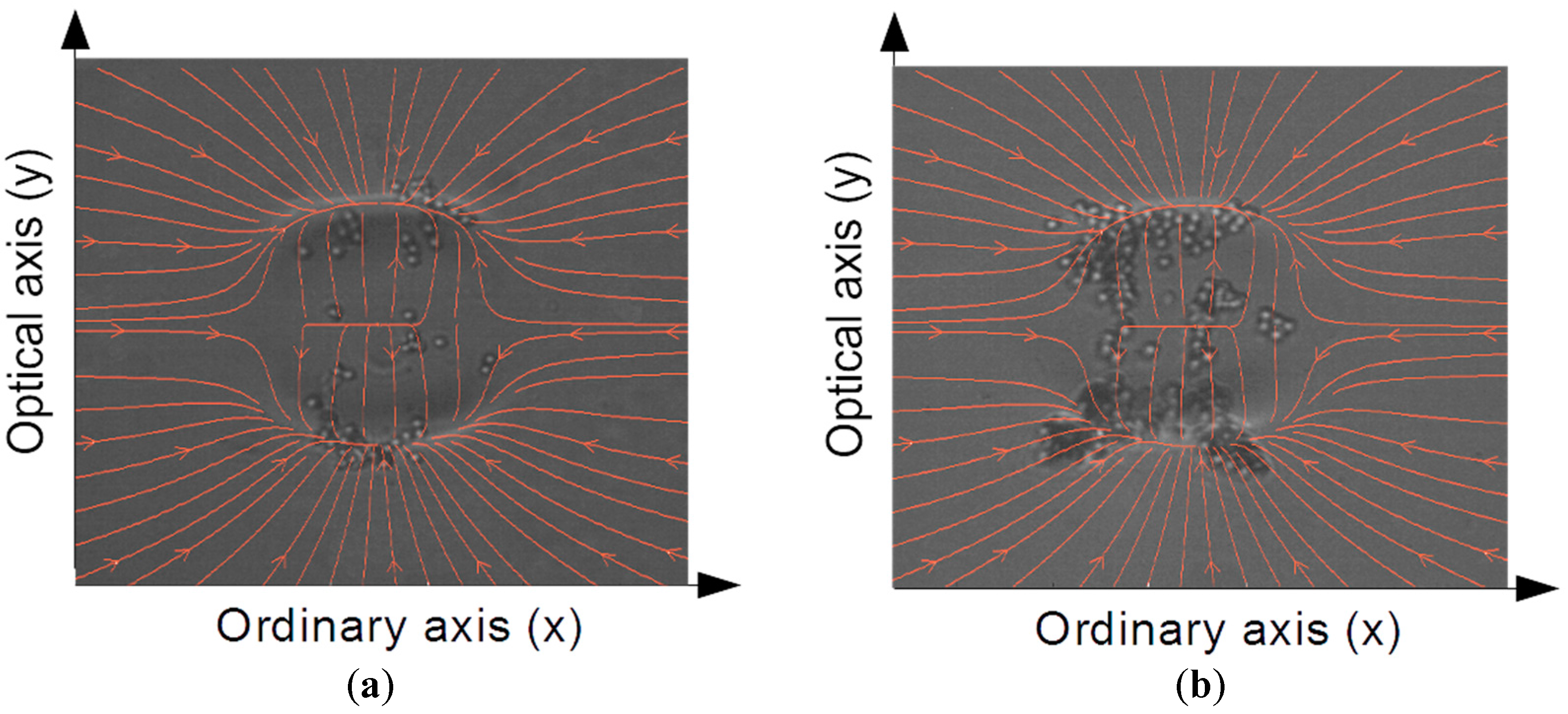
2.2. Numerical Analysis
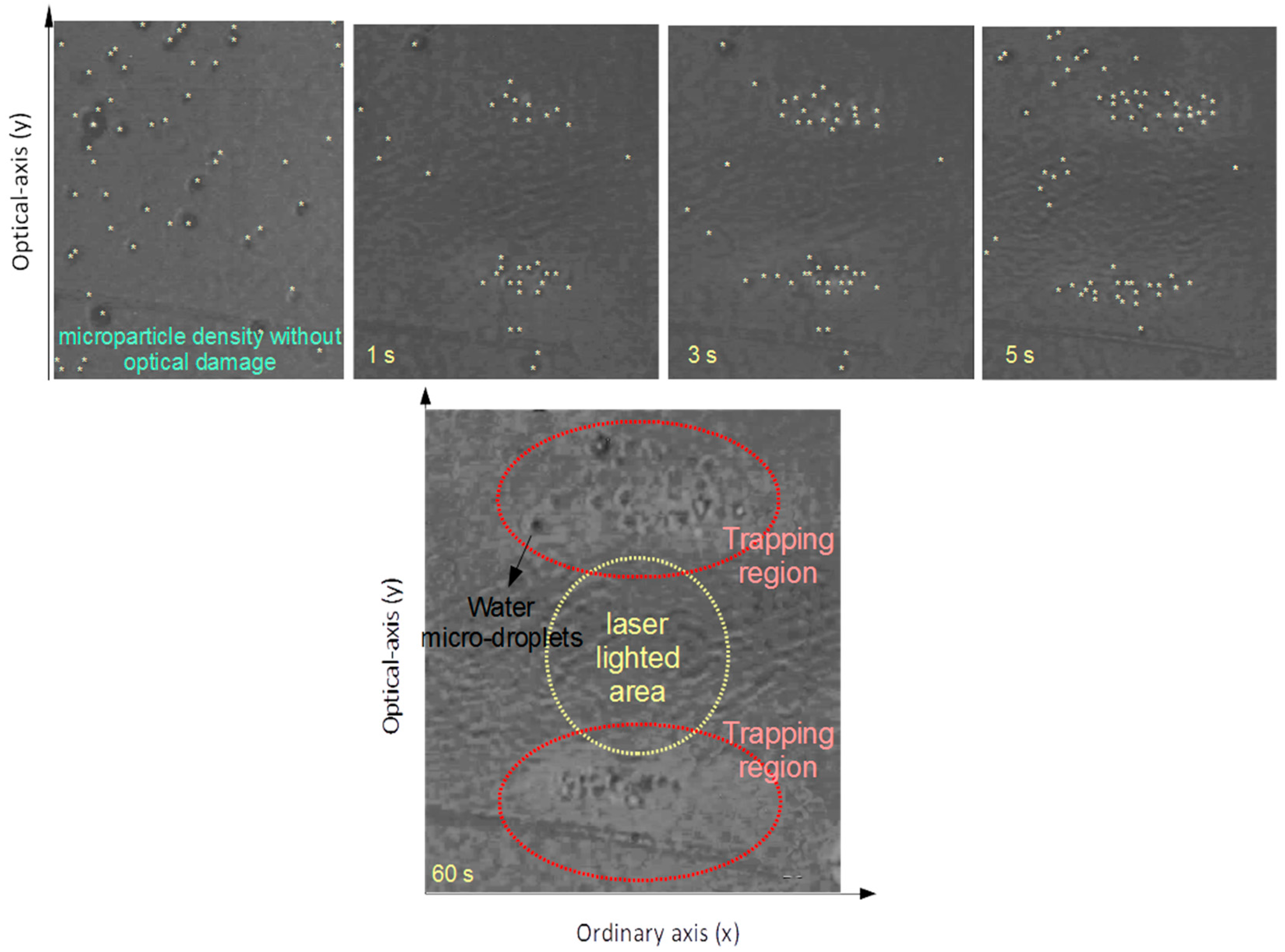
DEP forces are calculated considering, as a reference, 10 µm diameter particles suspended above the surface of a Fe:LiNbO3 crystal. The simulated system is shown in Figure 1. A continuous wave (CW) laser beam (Gaussian profile, w0 = 35 μm) with intensity I = 2600 W/cm2 impinges on the lower surface of a thin Fe:LiNbO3 substrate (size 350 × 450 × 700 μm3, x × y × z, representing a portion of the sample considered in the experiments) and propagates through the crystal along the z-direction, corresponding to a crystal ordinary axis. By considering a crystal thickness (t) much shorter than the beam Rayleigh range (zR), and considering a beam polarized along the crystal x axis (the other ordinary axis), it is possible to assume that the beam spatial profile remains unchanged during the propagation through the crystal, as the photorefractive effect only slightly affects the ordinary refractive index [35]. It must be noticed that these assumptions allow us to consider the beam propagation in the thin crystal slab as “homogeneous” along the z direction, i.e., we assume that for any value of z (in the crystal slab) the same distribution of space charge is produced by the photovoltaic effect.
On the upper surface of the crystal a buffer fluid of height 200 μm and permittivity ɛm, containing dielectric particles (ɛp), is considered; the “force investigation volume” is thus obtained as 350 × 450 × 200 μm3.
There are five main simulation steps required to evaluate the DEP force distribution, described in more details in the following: (i) calculation of the space-charge field (Esc) induced by the laser beam in a single x-y crystal-slab with 1-µm thickness; (ii) computation of the charge distribution Q(x,y) produced in the 1-µm-slab; (iii) calculation of the E-field produced in the space by the previously obtained Q(x,y); (iv) evaluation of the overall E-field by summing up the contributions of all the “1-µm-slabs” in which the crystal substrate is ideally divided; (v) determination of the DEP force field F(x,y,z).
As a first step, the 2D distribution of Esc can be calculated using Equation (2), with the conditions (3a) and (3b). An important parameter to be defined, so as to properly carry out the numerical simulations is the photovoltaic voltage Vph, appearing in (3b), which is responsible for the drift of the free charges generated under illumination of the sample [35]. In our simulations, such parameters can be considered constant, since we are dealing with high-intensity regime for Fe-doped LiNbO3 crystal, and we set it to 107 V/m [18].
Once Esc is known in the 1 µm high crystal slab, it is possible to evaluate the charge distribution Q(x,y), which is assumed to be described by a matrix of point-like charges lying in the crossing points of a 1 × 1 μm grid. This “charge map” was composed by calculating the charge contained in each “discrete element” (1 × 1 × 1 μm3) of the LiNbO3 slab. In particular, we used the integral form of Gauss’ theorem: we calculated the overall flux through the closed surface of each “discrete element” (only due to the x and y E-fields components, as the situation is considered to be uniform in the z direction), which is directly proportional, by the dielectric constant, to the net charge present in the unitary-cell volume.
Figure 2 reports, on the right side, the steady-state charge distribution: as expected the charge distribution is influenced by the presence of the photovoltaic field that makes the photo-induced charges separate along the optical axis direction, resulting in a net accumulation of the positive/negative charge along the borders of the illuminated area.
Starting from the obtained charge distribution Q(x,y), the third step of the process is to evaluate the E-field E(x,y,z) produced by the point-like charges of a 1-µm slab in the region above the crystal surface. The values of the three components of E(x,y,z) along the axes (x,y,z) are calculated by simply applying the point-charge approximation.
In order to obtain the total field E(x,y,z), produced by the whole crystal, we take advantage of the fact that the slab is assumed as “homogeneous” along the z direction. As each slab produces an identical E-field distribution in the space, apart from a translation along the z-direction, we calculate the overall E(x,y,z) present in a volume of 350 × 450 × 200 µm3, by summing up 700 (one for each slab composing the crystal) matrices for each layer of the investigated volume, simply “translated” in the z-direction.
In Figure 3 we show the electric field distribution 1 μm above the crystal surface (left) and on the top of the “investigation volume”, that is 200 μm above the surface (right). As expected, the total electric field decades rapidly while moving away from the crystal; such a fact is also evident plotting E(x,y,z) in the y-z plane cutting the middle of the beam, corresponding to x = 175 µm (central panel of Figure 3).
Finally, starting from the calculated E-field, the DEP force acting on a dielectric particle (with a given εp) in the region above the crystal (where a medium with given εm is present) was determined, as described in Section 2.1. As expected, stronger forces are present where the field gradient is larger and traps are found where the E-field amplitude corresponds to a local maximum. To graphically highlight the trapping positions, we show in Figure 4 the DEP force-lines obtained considering paraffin oil (εm = 2.2) and PMMA micro-particles (εp = 7.9) [36].
It is worth underlining that in this case a “trapping” (or “attractive”) configuration is obtained thanks to the fact that εp > εm; in the opposite case a “repulsive” configuration would be produced.

3. Discussions

In this section we discuss the experimental results obtained using materials with well-known dielectric properties: (i) PMMA spheres (10 µm diameter) in paraffin oil suspension; (ii) PMMA spheres in water suspension; (iii) water micro droplets (2–10 µm diameter) in paraffin oil.
In Figure 5 we show two images showing the optical trap created by a laser beam of intensity I = 2600 W/cm2 after 30 s of irradiation. The microparticles suspension was deposited on the substrate only after that the laser was switched off, thus avoiding possible heating effects, due to laser absorption, and any effect of photo-damaging of the suspended sample. This measurement protocol was selected in order to comply with the stringent requirements for cell preservations in future biological applications. Additionally, in order to evaluate a possible time-dependence of the effect, we also performed some experiments by waiting a few hours between creating the trap and applying the suspension, always obtaining consistent trapping results.
The PMMA microspheres in paraffin oil suspension are attracted to the bottom and top of the previously illuminated area, in correspondence of the same trap regions previously highlighted in the simulations. Furthermore, in (Video S1: MGazzetto_trapping), the particles remarkably follow the force lines geometry calculated in section 2.2.
The same experiments were also done with PMMA particles in Milli-Q water (characterized by a resistivity of 18 MΩ cm at 25 °C) to observe the repulsive behavior calculated before, and to explore the possibility of trapping in water. It was not possible to observe any effect different from thermal convection of the PMMA particles in water or any aqueous solution.
The main reason for such a phenomenon, (often simply explained considering that the forces are reduced because εwater ≈ 40 × εparaffin), is that even in ideally purified water, the natural ionization produces free carriers that can move in order to “screen” the crystal-charges distribution. As in our experiments, the volume of water used as a buffer fluid is a few µL, the free-ions charges are several orders of magnitude larger than the overall charges moved inside the crystal, thus allowing water to completely screen the space-charge field, and thus making this kind of approach impossible. Considering our experimental system, in order to realize effective trapping without modifying the substrate material or the beam characteristics, it would have been necessary to shrink the fluid volume to the fL scale, which is quite impractical in the macroscopic scale, but could be feasible and promising for applications in micro- or nano- fluidic integrated systems for sub-cellular components analysis.
Manipulating micro-scaled objects in water solution would be an important goal for future research on OET, especially in biological applications. We thus performed an additional experiment of water droplets micro-manipulation using as suspension liquid paraffin oil. Demineralized water micro-droplets were created by using a nebulizer, yielding to a droplet diameter in the range 2–10 µm. The micro-droplets were deposited in paraffin oil, making possible the reproduction of the same trapping experiment performed for PMMA micro-spheres in paraffin oil. Indeed, in this situation water micro-droplets undergo positive DEP (ɛp > ɛm) and, as it is shown in Figure 6, it is possible to achieve trapping regions in the upper and bottom side of the area illuminated by the laser beam. This result is very promising as the possibility to trap water micro-droplets in paraffin oil opens up new possibilities in the field of droplets micromanipulation, as well as for the manipulation of biological samples, which could be encapsulated in water droplets.

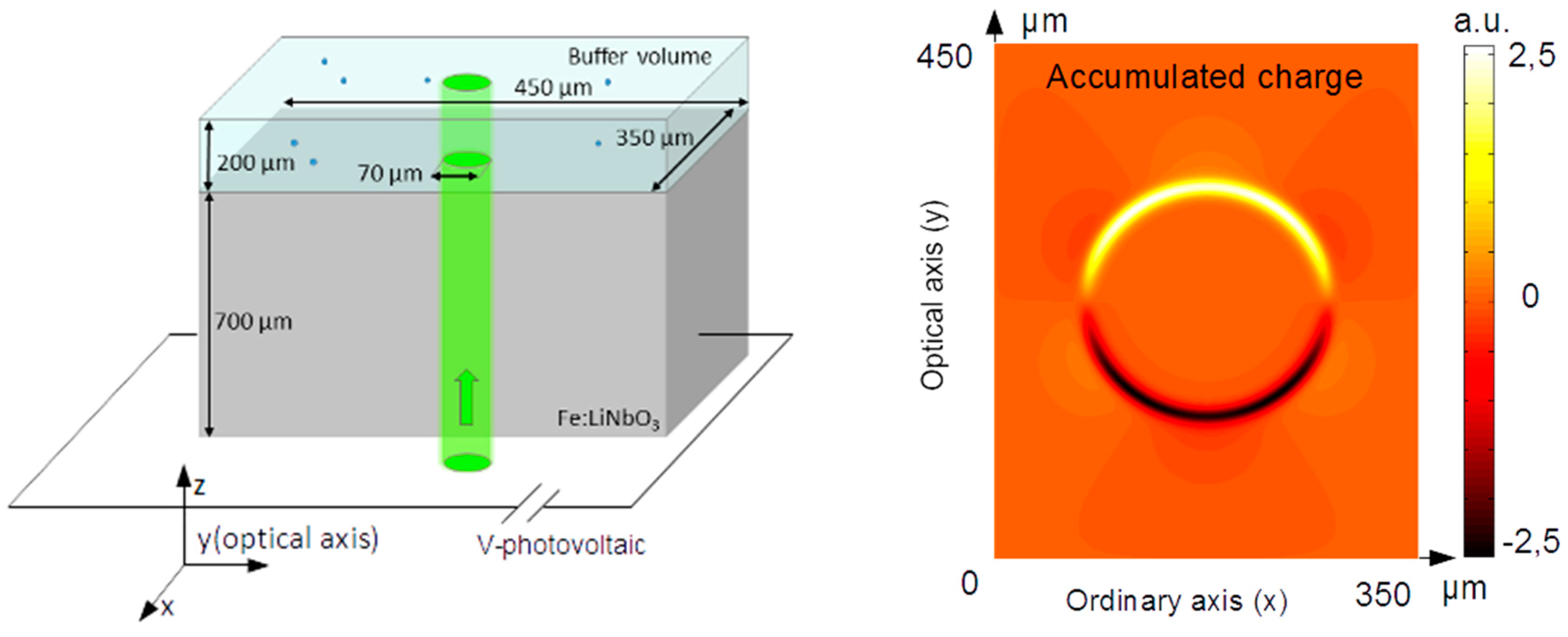
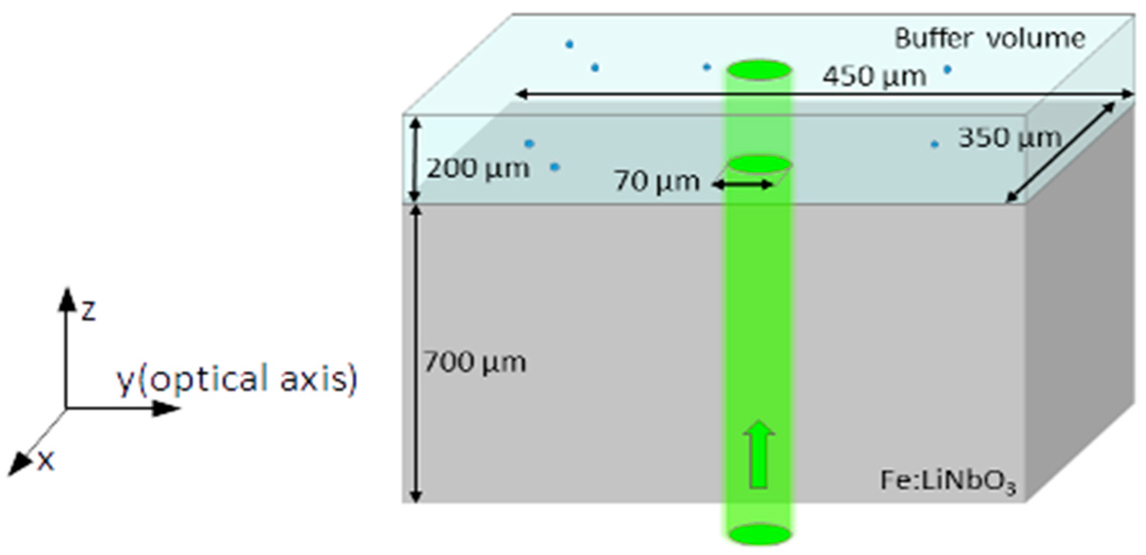
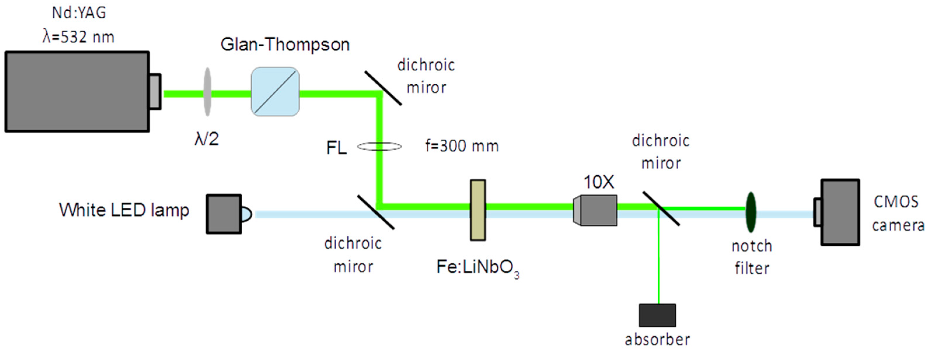
4. Materials and Methods

In order to verify the numerical simulations results, the corresponding experiments were carried out using the setup shown in Figure 7. The Fe:LiNbO3 sample (congruent composition; ciron = 18.8 × 1018 cm−3, 0.1% mol) used for the experiments was grown at the University of Padova by using the Czochralski technique. The growth direction was along the z-axis of the material and the Fe:LiNbO3 boule was poled in air atmosphere at 1200 °C to obtain a single domain structure. The boule was then oriented along the three main axes and the final sample was cut with the main face perpendicular to the y axis (“y-cut sample”).
The crystalline quality of the Fe:LiNbO3 crystal was checked to be comparable with that of commercial crystals, by using the High Resolution X-ray Diffraction technique. Finally, the sample was polished using a Logitech PM5 lapping machine (Logitech, UK) to achieve optical quality surfaces.
The resulting substrate, 700 µm thick, was illuminated by a frequency-doubled CW Nd: YAG laser emitting at 532 nm, and the effects produced on spherical beads dropped on the crystal were monitored by a CMOS camera (Thorlabs Inc., Newton, NJ, USA). We note that the space-charge electric field produced by the photorefractive effect can be erased by means of a uniform illumination or by controlled heating.
The focal length of lens FL was chosen in order to obtain the desired beam waist (w0 = 35 µm). The sample was irradiated in high intensity regime, with I = 2600 W/cm2 for a specified time interval (30 s), long enough to saturate the build-up of the space charge field [25]. The build-up of the space-charge E-field, and of the consequent refractive index modulation, was monitored through an imaging system composed by a generic white led lamp, a 10× objective (Thorlabs Inc., Newton, NJ, USA), and a CMOS camera; a dichroic mirror and a notch filter (both by Thorlabs Inc., Newton, NJ, USA) were used to prevent the laser beam from reaching the camera. The laser was then switched off and a small drop (about 10 µL) of micro-particle suspension was deposited on the crystal surface; thanks to the imaging system it was possible to monitor in real time the micro-particles movement and trapping produced by DEP forces.

5. Conclusions

A direct comparison between numerical simulations and experimental measurements on particle trapping on the surface of a Fe-doped Lithium Niobate crystal was presented. Given the intensity distribution profile of the laser beam inducing the photovoltaic field used to trap particles, we estimated the trapping regions and the geometric properties of the DEP forces applied to a dielectric particles suspension, which were confirmed by the experimental results obtained with PMMA microspheres in paraffin oil suspension. In addition, we highlight that no trapping or repulsive DEP force was ever observed for micro-particles in aqueous medium. However, to overcome this problem a different approach was followed, by using micro-droplets of demineralized water suspended in paraffin oil. In this way it was possible to successfully trap water micro-droplets in the areas predicted by the numerical simulations. This result is remarkable, since it finally paves the way to future biological light-driven applications in Lithium Niobate.

Supplementary Materials

The following are available online at https://www.mdpi.com/2073-4352/6/10/123/s1, Video S1: MGazzetto_trapping.

Acknowledgments

The activity was supported by the Cost Action MP1205, 2012–2016 (“Advances in optofluidics”).

Author Contributions

All the authors participated in conceiving and designing the experiments; the crystal samples were prepared and characterized by Annamaria Zaltron and Cinzia Sada; Michela Gazzetto and Giovanni Nava performed the experiments; the numerical simulations were carried out by Michela Gazzetto, with the help of Giovanni Nava and Paolo Minzioni; Michela Gazzetto, Paolo Minzioni and Giovanni Nava analyzed the data; all the authors participated in extensive discussions and jointly wrote the paper.

Conflicts of Interest

The authors declare no conflict of interest. The founding sponsors had no role in the design of the study; in the collection, analyses, or interpretation of data; in the writing of the manuscript, and in the decision to publish the results.

References

  1. Figeys, D.; Pinto, D. Lab-on-a-chip: A revolution in biological and medical sciences. Anal. Chem. 2000, 72, 330A–335A. [Google Scholar] [CrossRef] [PubMed]
  2. Grier, D.G. A revolution in optical manipulation. Nature 2003, 424, 810–816. [Google Scholar] [CrossRef] [PubMed]
  3. Ashkin, A.; Dziedzic, J.M.; Bjorkholm, J.E.; Chu, S. Observation of a single-beam gradient force optical trap for dielectric particles. Opt. Lett. 1986, 11, 288–290. [Google Scholar] [CrossRef] [PubMed]
  4. Craighead, H. Future lab-on-a-chip technologies for interrogating individual molecules. Nature 2006, 442, 387–393. [Google Scholar] [CrossRef] [PubMed]
  5. Liberale, C.; Cojoc, G.; Bragheri, F.; Minzioni, P.; Perozziello, G.; La Rocca, R.; Ferrara, L.; Rajamanickam, V.; Di Fabrizio, E.; Cristiani, I. Integrated microfluidic device for single-cell trapping and spectroscopy. Sci. Rep. 2013, 3. [Google Scholar] [CrossRef] [PubMed]
  6. Yang, T.; Paiè, P.; Nava, G.; Bragheri, F.; Vazquez, R.M.; Minzioni, P.; Veglione, M.; Di Tano, M.; Mondello, C.; Osellame, R.; et al. An integrated optofluidic device for single-cell sorting driven by mechanical properties. Lab Chip 2015, 15, 1262–1266. [Google Scholar] [CrossRef] [PubMed]
  7. Yang, T.; Nava, G.; Minzioni, P.; Veglione, M.; Bragheri, F.; Lelii, F.D.; Vazquez, R.M.; Osellame, R.; Cristiani, I. Investigation of temperature effect on cell mechanics by optofluidic microchips. Biomed. Opt. Express 2015, 6, 2991–2996. [Google Scholar] [CrossRef] [PubMed]
  8. Shenoy, A.; Rao, C.V.; Schroeder, C.M. Stokes trap for multiplexed particle manipulation and assembly using fluidics. Proc. Natl Acad. Sci. USA 2016, 113, 3976–3981. [Google Scholar] [CrossRef] [PubMed]
  9. Khoshmanesh, K.; Nahavandi, S.; Baratchi, S.; Mitchell, A.; Kalantar-zadeh, K. Dielectrophoretic platforms for bio-microfluidic systems. Biosens. Bioelectron. 2011, 26, 1800–1814. [Google Scholar] [CrossRef] [PubMed]
  10. Chiou, P.Y.; Ohta, A.T.; Wu, M.C. Massively parallel manipulation of single cells and microparticles using optical images. Nature 2005, 436, 370–372. [Google Scholar] [CrossRef] [PubMed]
  11. Pohl, H.A. Some effects of nonuniform fields on dielectrics. J. Appl. Phys. 1958, 29, 1182–1188. [Google Scholar] [CrossRef]
  12. Eggert, H.A.; Kuhnert, F.Y.; Buse, K.; Adleman, J.R.; Psaltis, D. Trapping of dielectric particles with light-induced space-charge fields. Appl. Phys. Lett. 2007, 90, 241909. [Google Scholar] [CrossRef]
  13. Esseling, M.; Holtmann, F.; Woerdemann, M.; Denz, C. Two-dimensional dielectrophoretic particle trapping in a hybrid crystal/PDMS-system. Opt. Express 2010, 18, 17404–17411. [Google Scholar] [CrossRef] [PubMed]
  14. Sturman, P.J. Photovoltaic and Photo-refractive Effects in Noncentrosymmetric Materials; CRC Press: Philadelphia, PA, USA, 1992; Volume 8. [Google Scholar]
  15. Volk, T.R.; Wöhlecke, M. Optical damage resistance in lithium niobate crystals. Ferroelectr. Rev. 1998, 1, 195–262. [Google Scholar]
  16. Razzari, L.; Minzioni, P.; Cristiani, I.; Degiorgio, V.; Kokanyan, E.P. Photorefractivity of Hafnium-doped congruent lithium–niobate crystals. Appl. Phys. Lett. 2005, 86, 131914. [Google Scholar] [CrossRef]
  17. Zhang, X.; Wang, J.; Tang, B.; Tan, X.; Rupp, R.A.; Pan, L.; Kong, Y.; Sun, Q.; Xu, J. Optical trapping and manipulation of metallic micro/nanoparticles via photorefractive crystals. Opt. Express 2009, 17, 9981–9988. [Google Scholar] [CrossRef] [PubMed]
  18. Esseling, M.; Zaltron, A.; Argiolas, N.; Nava, G.; Imbrock, J.; Cristiani, I.; Sada, C.; Denz, C. Highly reduced iron-doped lithium niobate for optoelectronic tweezers. Appl. Phys. B 2013, 113, 191–197. [Google Scholar] [CrossRef]
  19. Esseling, M.; Zaltron, A.; Sada, C.; Denz, C. Charge sensor and particle trap based on z-cut lithium niobate. Appl. Phys. Lett. 2013, 103, 06115. [Google Scholar] [CrossRef]
  20. Esseling, M.; Zaltron, A.; Horn, W.; Denz, C. Optofluidic droplet router. Laser Photon. Rev. 2015, 9, 98–104. [Google Scholar] [CrossRef]
  21. Zaltron, A.; Bazzan, M.; Argiolas, N.; Ciampolillo, M.V.; Sada, C. Depth-resolved photorefractive characterization of lithium niobate doped with iron by thermal diffusion. Appl. Phys. B 2012, 108, 657–663. [Google Scholar] [CrossRef]
  22. Peithmann, K.; Wiebrock, A.; Buse, K. Photorefractive properties of highly-doped lithium niobate crystals in the visible and near-infrared. Appl. Phys. B 1999, 68, 777–784. [Google Scholar] [CrossRef]
  23. Volk, T.; Wöhlecke, M. Lithium Niobate: Defects, Photorefraction and Ferroelectric Switching; Springer Science & Business Media: Berlin, Germany, 2008; Volume 115. [Google Scholar]
  24. Villarroel, J.; Burgos, H.; García-Cabañes, Á.; Carrascosa, M.; Blázquez-Castro, A.; Agulló-López, F. Photovoltaic versus optical tweezers. Opt. Express 2011, 19, 24320–24330. [Google Scholar] [CrossRef] [PubMed]
  25. Arregui, C.; Ramiro, J.B.; Alcázar, Á.; Méndez, Á.; Burgos, H.; García-Cabañes, Á.; Carrascosa, M. Optoelectronic tweezers under arbitrary illumination patterns: Theoretical simulations and comparison to experiment. Opt. Express 2014, 22, 29099–29110. [Google Scholar] [CrossRef] [PubMed]
  26. Miccio, L.; Memmolo, P.; Grilli, S.; Ferraro, P. All-optical microfluidic chips for reconfigurable dielectrophoretic trapping through SLM light induced patterning. Lab Chip 2012, 12, 4449–4454. [Google Scholar] [CrossRef] [PubMed]
  27. Muñoz-Martínez, J.F.; Jubera, M.; Matarrubia, J.; García-Cabañes, A.; Agulló-López, F.; Carrascosa, M. Diffractive optical devices produced by light-assisted trapping of nanoparticles. Opt. Lett. 2016, 41, 432–435. [Google Scholar]
  28. Carrascosa, M.; García-Cabañes, A.; Jubera, M.; Ramiro, J.B.; Agulló-López, F. LiNbO3: A photovoltaic substrate for massive parallel manipulation and patterning of nano-objects. Appl. Phys. Rev. 2015, 2, 040605. [Google Scholar] [CrossRef]
  29. Ferraro, P.; Grilli, S.; Miccio, L.; Vespini, V. Wettability patterning of lithium niobate substrate by modulating pyroelectric effect to form microarray of sessile droplets. Appl. Phys. Lett. 2008, 92, 213107. [Google Scholar] [CrossRef]
  30. Ferraro, P.; Coppola, S.; Grilli, S.; Paturzo, M.; Vespini, V. Dispensing nano-pico droplets and liquid patterning by pyroelectrodynamic shooting. Nat. Nanotechnol. 2010, 5, 429–435. [Google Scholar] [CrossRef] [PubMed]
  31. Jones, T.B. Electromechanics of Particles; Cambridge University Press: Cambridge, UK, 1995. [Google Scholar]
  32. Kukhtarev, N.V.; Markov, V.B.; Odulov, S.G.; Soskin, M.S.; Vinetskii, V.L. Holographic storage in electrooptic crystals. I. Steady state. Ferroelectrics 1978, 22, 949–960. [Google Scholar] [CrossRef]
  33. DelRe, E.; Ciattoni, A.; Crosignani, B.; Tamburrini, M. Approach to space-charge field description in photorefractive crystals. J. Opt. Soc. Am. B 1998, 15, 1469–1475. [Google Scholar] [CrossRef]
  34. Crognale, C.; Rosa, L. Vector analysis of the space-charge field in nonconventionally biased photorefractive crystals. J. Lightwave Technol. 2005, 23, 2175–2185. [Google Scholar] [CrossRef]
  35. Günter, P.; Huignard, J.-P. Photorefractive Materials and Their Applications; Günter, P., Huignard, J.-P., Eds.; Springer: Berlin, Germany, 1989; Volume 2. [Google Scholar]
  36. Khan, F.L.A.; Sivagurunathan, P.; Kamil, S.R.M.; Mehrotra, S.C. Dielectric studies of methyl methacrylate and butyl methacrylate with primary alcohols using time domain reflectometry. Indian J. Pure Appl. Phys. 2007, 45, 754. [Google Scholar]
Figure 1. Scheme of the geometry considered for numerical simulation.
Crystals 06 00123 g001
Figure 2. Scheme of the ideal system, including a photovoltaic potential generator, considered to evaluate Q(x,y) (on the left) and space charge distributions obtained considering the above reported data (on the right).
Crystals 06 00123 g002
Figure 3. Simulation of the electric field above the photorefractive crystal, underlying the field lines. Left: E-field calculated on the transversal x-y plane located 1 µm above the crystal. Right: E-field on the x-y plane 200 µm above the crystal. It is interesting to notice that close to the crystal surface the E-field decreases from about 50 kV/m to less than 4 kV/m within a 200 µm range along the optical axis. Center: E-field distribution estimated in the y-z vertical plane corresponding to the center of the beam at x = 175 µm.
Crystals 06 00123 g003
Figure 4. Simulation of the dielectrophoretic (DEP) force in the x-z layer 1 µm above the sample surface and in the y-z layer for x = 175 µm.
Crystals 06 00123 g004
Figure 5. Two example of superposition of numerical simulation results and the experimental images obtained for PMMA spheres in paraffin oil, (a,b) were obtained by repeating the same experiment twice while increasing the beads density.
Crystals 06 00123 g005
Figure 6. Top: sequence of frames showing the water-droplet movement in paraffin-oil towards the trapping area. The center of each droplet is marked with a small white star to highlight their positions and movement. It can be observed that an increasing number of droplets are attracted in the camera’s area. Bottom: overview of the optical damage with trapped water micro-droplets.
Crystals 06 00123 g006
Figure 7. Scheme of the setup developed for experiment of optical trapping on a lithium niobate crystal, with the laser propagating in a plane perpendicular respect to the large faces of the y-cut sample.
Crystals 06 00123 g007

