
Band Structure of Photonic Crystals Fabricated by Two-Photon Polymerization

Abstract
: We study theoretically the band-gap structures of several types of three-dimensional photonic crystals with the fcc lattice symmetry: synthetic opals, inverted yablonovite and woodpile. The samples of inverted yablonovite, inverted yablonovite with a glassy superstructure and woodpile are fabricated by two-photon polymerization through a direct laser writing technique, which allows the creation of complex three-dimensional photonic crystals with a resolution better than 100 nm. A material is polymerized along the trace of a moving laser focus, thus enabling the fabrication of any desirable three-dimensional structure by direct “recording” into the volume of a photosensitive material. The correspondence of the structures of the fabricated samples to the expected fcc lattices is confirmed by scanning electron microscopy. We discuss theoretically how the complete photonic band-gap is modified by structural and dielectric parameters. We demonstrate that the photonic properties of opal and yablonovite are opposite: the complete photonic band gap appears in the inverted opal, and direct yablonovite is absent in direct opal and inverted yablonovite.1. Introduction
Periodic order in a photonic crystal provides coherent scattering of light from a precise geometrical arrangement of identical scatterers that leads to the formation of band gaps, where destructive wave interference prevents light propagation in specific directions or the formation of the omnidirectional complete photonic band gap over a specific energy range. In the simplest case of a small dielectric contrast, band gaps are associated with the Bragg reflection of light from systems of planes of the photonic crystal lattice. As a result, the transport of the light outside band gaps has a ballistic character, whereas the localization of the light is observed in the region of band gaps [1,2]. Now, investigation of photonic crystals has become one of the modern rapidly developing directions in solid state physics [3–5].
In 1991, Yablonovitch et al. [6] demonstrated the first artificial 3D photonic crystal, which was called, more recently, yablonovite [3,7]. Yablonovite is a dielectric matrix drilled in three directions coinciding with three vectors of a unit cell of the fcc lattice. Such a structure is called direct yablonovite, implying that inverted yablonovite is the structure of filled holes and the air matrix surrounding them. The method of fabrication of original yablonovite proposed in [6], i.e., mechanical drilling of millimeter cylindrical holes in an insulator, determines the microwave spectral range for the photonic band gap, which for the relative permittivity ε = 13 typical of semiconductors, is formed between the second and third photonic branches, with the width being about 20% of its central frequency.
However, the expansion of the photonic band structure to the infrared and visible spectral ranges faced serious technological difficulties. The most convenient technology for the fabrication of 3D photonic crystals for the visible range is the self-assembling growth of colloidal crystal. The well-known members of the colloidal crystal’s family are natural and artificial opals [8]. Opals are made up of nearly spherical particles of amorphous silica a-SiO2 of several hundred nanometers in diameter, which tend to form by self-assembling a close-packed structure with symmetry, to a first approximation, of an fcc lattice. Opals have voids between a-SiO2 spheres, which could be filled by liquid or solid fillers with controlled permittivity values [9–14]. After the opals were found to be 3D PhCs in the visible spectral region [8], inverted opals were synthesized [15–17] with a complete photonic band predicted in [18,19]. The photonic band structure of opals, i.e., the wave vector dependence of the band gaps energy in all high-symmetry directions on the Brillouin zone (BZ), was first experimentally investigated in [10,12]. Unfortunately, all self-assembling crystals, including opals, are characterized by a large concentration of lattice defects and, especially, planar stacking faults. Even in the most perfect samples of opals, it is impossible to completely avoid different defects. In particular, the inhomogeneity of the permittivity over the volume of each individual a-SiO2 particle [13,14,20], as well as a dispersion in the size and permittivity in the ensemble of a-SiO2 particles forming a particular sample of opal [9,14,21–23] is unremovable.
The problem of the fabrication of defect-free photonic crystals of almost arbitrary shape and various dimensions can be solved with the recently developed method of 3D laser lithography, which is also called direct laser writing [24–26]. This method is based on the nonlinear two-photon polymerization of a photosensitive material in the focus of a femtosecond laser beam. In two-photon polymerization, nearly simultaneous absorption of two photons within a small volume in a photosensitive material induces chemical reactions between photo-initiator molecules and monomers, which converts a liquid or gel monomer into a solid polymer. In order to obtain a photonic crystal filled with air, after the polymerization process, the material that was not exposed to an intense laser irradiation should be washed out with the developer [27]. The high resolution of the method is due to the intensity-threshold character of the polymerization process, which occurs in a region with sizes significantly smaller than the size of the focused beam. This technique makes it possible to form a 3D photonic crystal with a transverse resolution below 100 nm [26,28–30].
The unique capability of the direct laser writing method lies in that it allows the fabrication of computer-designed 3D structures of almost arbitrary shape with resolution beyond the diffraction limit. Widely used prototyping techniques, such as 3D inkjet printing and UV laser stereo-lithography, can also produce 3D structures; however, they cannot provide resolution better than a few microns. Lithographic techniques with extremely high resolution, such as e-beam lithography, are limited to producing 2D structures. Moreover, using direct laser writing technique, one can introduce defects into 3D photonic crystals or design a structure with a disordered glassy superstructure; something not possible using other methods [31,32].
2. Photonic Crystals Fabricated by Two-Photon Polymerization
To realize the two-photon polymerization technique for the fabrication of the woodpile photonic crystals, we use a train of femtosecond pulses centered at around 780 nm wavelength and at a repetition frequency of 80 MHz (12.5 ns of time between adjacent pulses). These pulses are derived from a 50-fs TiF-100F laser emitter (Avesta-Project, Moscow, Russia). Laser radiation was focused in the photoresist volume through the glass substrate with a 100× oil-immersion microscope objective with numerical aperture NA = 1.4 (Carl Zeiss MicroImaging GmbH, Jena, Germany). The structure was created using a hybrid organic-inorganic material based on zirconium propoxide with an Irgacure 369 photo-initiator (Ciba Specialty Chemicals Inc., Basel, Switzerland). The advantage of this material is low shrinkage upon polymerization, which guarantees a perfect correspondence of the resulting structure to a suggested mathematical model [26]. To fabricate structures, a photoresist drop was deposited on the surface of a glass substrate 150 μm thick and was dried at 60 °C for 30 min. The employed material is transparent for the used near-infrared laser radiation; therefore, only two-photon absorption can initiate a photo-polymerization process.
Due to the threshold behavior and nonlinear nature of the two-photon polymerization, the light-material interaction region is confined to the small volume within the focus of the laser beam. Resolution beyond the diffraction limit can be realized by controlling the laser pulse energy. The minimum structural feature volume is dependent on several parameters, including laser power, numerical aperture of the objective lens, exposure time, voxel-voxel distance, etc. A voxel, i.e., volumetric pixel, is defined as the unit volume of material cured by the two-photon polymerization process. The highest resolution can be achieved through the use of low exposure time and low laser power at an energy that is near the threshold energy.
Using the two-photon polymerization technology, 3D structures can be fabricated by moving the laser beam focus three-dimensionally through the photoresist volume. Note that there is a compromise between the resolution and sophistication of the structure on one side and processing time on the other side; more complicated shapes of the created structures require longer processing times.
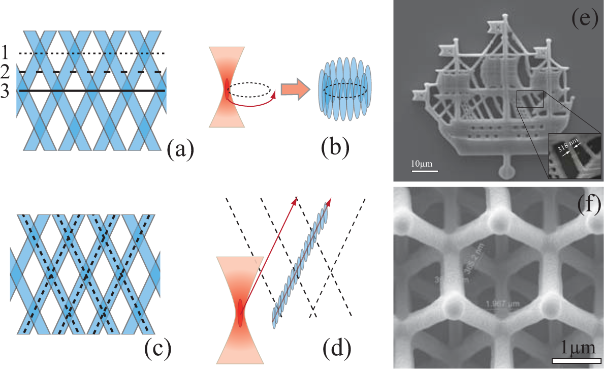
Different structures may be fabricated by means of either raster scanning or vector scanning. In the raster scanning approach, the structure is created in a layer-by-layer format. The scanning path of the laser focus is moved along a 2D scanning path in the xy-plane, while translation of the beam spot in the z-axis enables processing of 3D structures (Figure 1a,b). For this purpose, the sample was mounted on a two-coordinate motorized linear air-bearing translator (Aerotech Inc., Lexington, KY, USA). To avoid the distortion of the focused laser beam by the built structures, 3D structures are fabricated layer-by-layer from bottom to top. The motion of the translators is controlled by a computer with software developed at Laser Zentrum Hanover. This software makes it possible to convert a computer model of the fabricated structure represented in the STLformat to the corresponding trajectory of the motion of the motorized mirror and stages. The raster scanning approach is appropriate for creating structures with complicated shapes. An example of such a structure is presented in Figure 1e and Figure 2d–f. This little ship is a micro-copy of a famous Saint Petersburg (Russia) landmark—the weather-vane from the top of the Admiralty tower.
The vector scanning approach is based on the geometric modeling of the periodic structure. The structure is defined by the vectors of translations, and voxels are superimposed along the required lines. This approach is ideally suited for creating different photonic crystals, as demonstrated in Figure 1f by the example of the inverted yablonovite structure. In the woodpile, the rods in adjacent layers are rotated by 90° relative to each other, and every other layer is shifted by half the rods’ spacing in the direction that is orthogonal to the rods [33–35]. Vector scanning enables structures to be fabricated in a more rapid manner, which is especially important in the case of the preparation of large photonic structures for optical measurements and different applications.
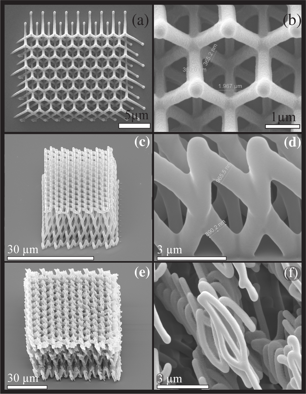
Aside from the problem of the perfect choice of the scanning approach, we must define the boundary of the normal exposure region depending on an average laser power and the structuring speed of the translators. To vary the laser power in the volume of the photoresist, we used a polarizer and half-wave plate situated on a computer-controlled motorized rotary table. An acousto-optic modulator was used to rapidly control the switching on/off of the laser beam. Figure 2 demonstrates the scanning electron microscopy images of the woodpile structure and the little ship obtained at different regimes, including low-, normal- and high-exposure for the woodpile.
In this paper, we discuss the photonic band structures of direct and inverted opals, yablonovite and woodpile structures. The inverted yablonovite structure was fabricated using the vector scanning approach (Figure 3a,b) [36] and the raster scanning approach (Figure 3a,b) [7]. In the raster scanning approach, the software formed cross-sections of the inverted yablonovite structure in the xy planes distributed with a specified step in the z direction and sequentially executed scanning in each of the planes. In order to decrease the fabrication time, the scanning in each xy plane was carried out only in closed contours bounding the structure. In the case of the inverse yablonovite, these contours had the form of circles (Figure 1b). The calculated filling factor of the structure is about 15%. Additionally to the perfect inverted yablonovite structure, the 3D disordered glass-like inverted yablonovite structure can be fabricated by the two-photon polarization technique (Figure 3e,f) [37]. No other competing technology offers such a possibility.
3. Theoretical Analysis of the Photonic Band Structures
To theoretically analyze the features of the band structure of the photonic crystals with the fcc lattice, we calculated the electromagnetic eigenmodes using the vector plane wave method. Following the approach proposed in [38], the magnetic field in the periodic structure can be represented in the reciprocal space basis as:
Here, c is the speed of light in a vacuum and is the positive semidefinite Hermitian operator, whose matrix elements Mg′,g determine the operator −(g′ + k) × εg′−g(g + k) × that acts on the vector hk,g (where εg is the Fourier transform of the inverse relative permittivity). As was shown in [39], it is convenient to calculate the action of the operator on a periodic vector function hk with two fast Fourier transforms (the first and second transforms are performed before and after multiplication by the relative permittivity, respectively). It is noteworthy that the function hk should satisfy not only Equation (1), but also the condition of the transversality of electromagnetic waves. In the chosen plane wave basis, this condition is reduced to the orthogonality of the Fourier transform hk,g and vector g + k.
A series of the lowest eigenfrequencies that is a solution of problem Equation (1) was obtained with a variant of the Lanczos procedure [40]. To accelerate the convergence of the algorithm, the subspace of approximants was expanded by an operator close to (this operator was described in [41]). In addition, to reduce the number of plane waves (i.e., the number of reciprocal lattice vectors used in expansion Equation (1)), we applied the effective dielectric tensor method [39,41]. The effective dielectric tensor at a certain point is determined by calculating the gradient of the permittivity by the finite difference method on a fine mesh near this point.
In order to compare the photonic properties of different fcc structures, we performed the calculation of the electromagnetic eigenmodes using the vector plane-wave method [7,36,42]. For comparison and analysis, we calculated the photonic band structure for direct and inverted opals and yablonovite, as well as for the woodpile structure. The frequencies of the eigenstates were calculated as a function of the wave vector k in the range of 0.0 < a/λ < 1.0. The eigenvalue problem was solved with 203 plane waves in expansion Equation (1) in the reciprocal lattice vectors that are inside the parallelepiped constructed on the primitive reciprocal lattice vectors (the length of the side of the parallelepiped was 20 primitive reciprocal lattice vectors). To calculate the effective dielectric tensor, the unit cell was divided into 1003 elements (using a 100 × 100 × 100 mesh).
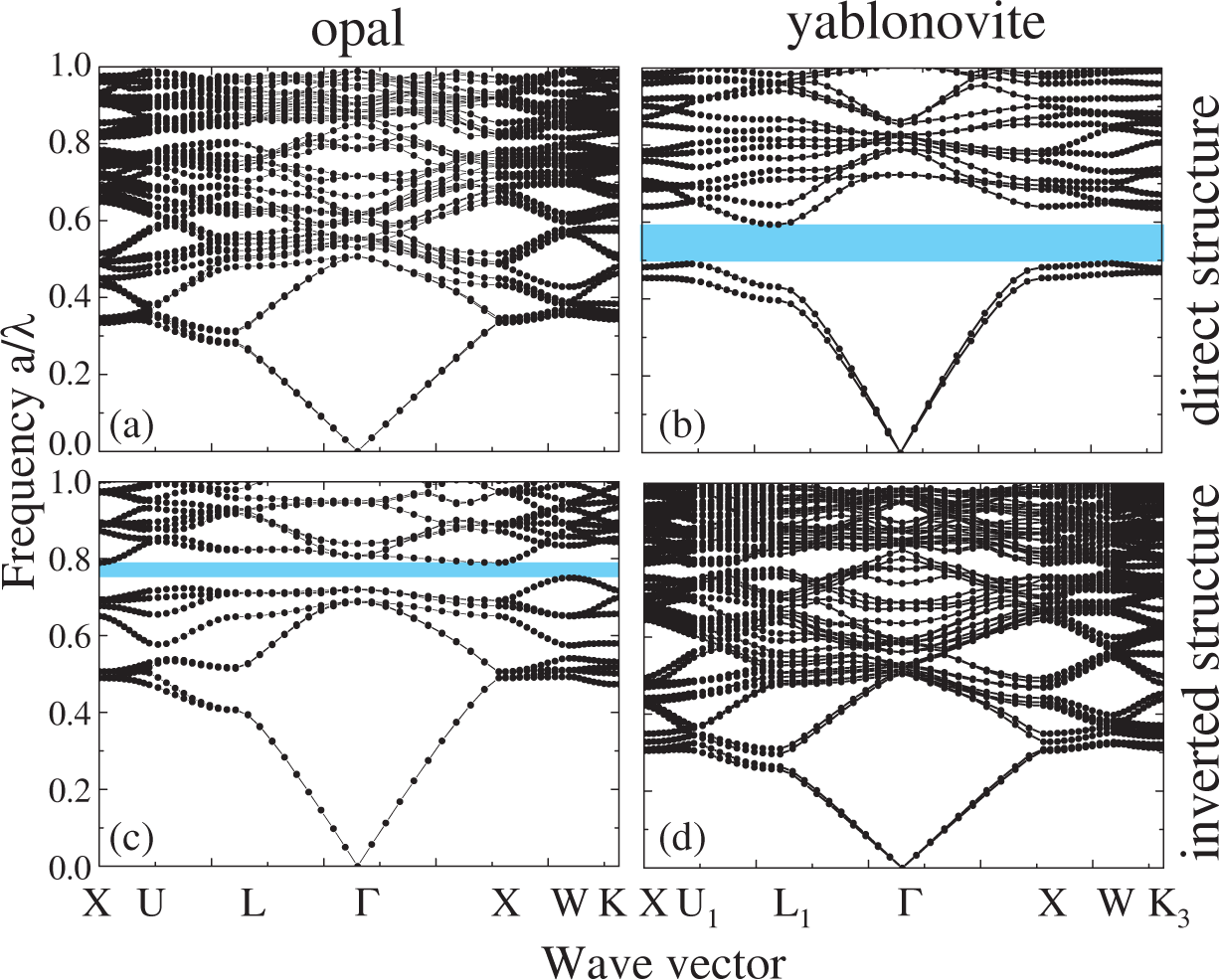
Figures 4 and 6 show the calculation results. Figure 4 presents the photonic band structure for the four discussed photonic crystals with the fcc lattice. As can be seen in the figure, the complete band gap is observed for inverted opal and direct yablonovite with a sufficiently high dielectric contrast. Any complete band gap is absent for direct opal (Figure 4a) and inverted yablonovite (Figure 4e). In the inverted opal structure, the lower gap edge is located in the W direction and the upper edge in X direction; in the direct yablonovite structure, the lower gap edge is located in the W direction and the upper edge in the L direction. Our results (Figure 4) coincide with those reported in the literature [3,6,18,19]: for inverted opals, the complete band gap appears between the eighth and ninth photonic branches with a center frequency of a/λ = 0.794; for direct yablonovite, the complete band gap appears between the second and third photonic branches with a center frequency of a/λ = 0.543.
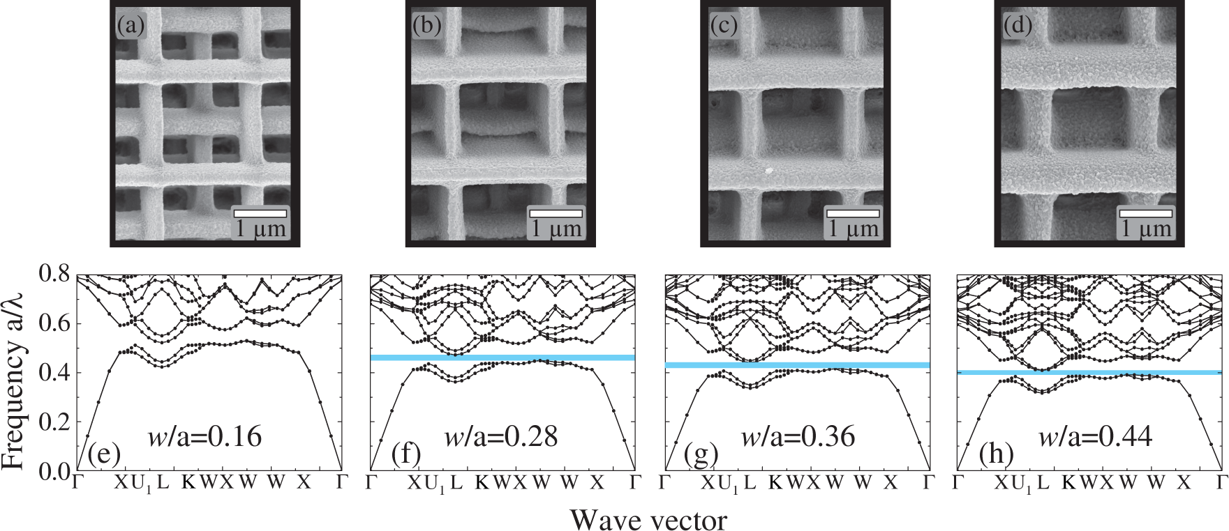
Figure 5 demonstrates the scanning electron microscopy images of a set of woodpile structures with different filling factors obtained by changing the rod cross-section to a lattice constant ratio. We fabricated woodpile structures composed of orthogonal rods with variable width w and a height of c/4 with lattice constants a = 2000 nm and c = 2800 nm (the case of when the woodpile structure has the symmetry of the fcc lattice). The photonic band structure has been calculated with the same relative permittivity ε = 6. As can be seen from the figure, there is a strong dependence of the complete band gap size on the filling factor that is presented in detail in Figure 6.
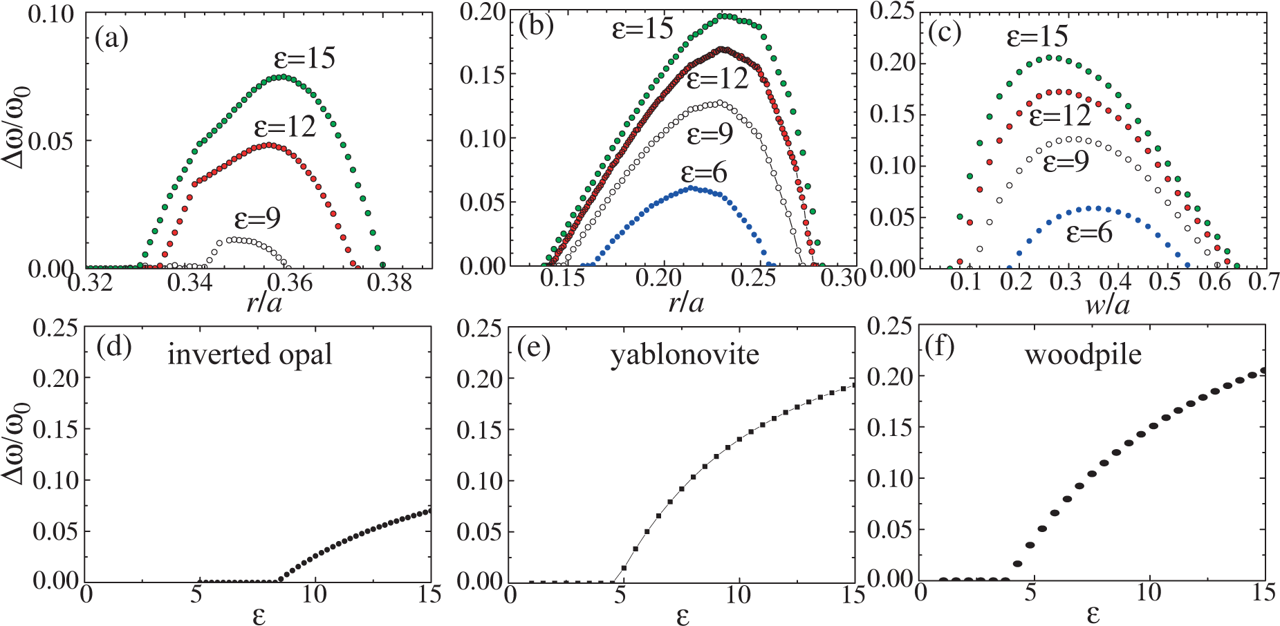
The relations of the structural and dielectric parameters to the relative complete band gap size Δω/ω0 for inverted opals, direct yablonovite and woodpile are presented in Figure 6. Note that the only difference between direct and inverted woodpile lattice is the filling factor of the structure. It can be seen that the complete band gap in the host permittivity scale appears in woodpile with square rods at ε = 4.6, in direct yablonovite with w/a = 0.23 at ε = 4.8 and in inverted opals at ε = 8.7. For all structures, an increase in the permittivity ε is accompanied by the monotonic expansion of the region of existence of the complete band gap (in the ε range under study). Obviously, at any given dielectric contrast, there exists an optimal filling ratio that maximizes the complete band gap. For example, at ε = 15, the structural configuration that would yield the largest gap is obtained when the air spheres in inverted opals have a diameter of about 0.36a, the cylindrical rods in direct yablonovite have a diameter of about 0.23a and the square rods in the fcc woodpile structure have width of about 0.28a. Note that the optimal value of r = 0.23a in the yablonovite structure corresponds to the filling factor of f = 25% (i.e., 75% of the volume of the sample is filled with air). Such a filling factor is very closeto the natural filling factor of opals, where the air spheres in the inverted opal fcc lattice at their point ofcontact occupy 74% of the volume of the sample.
4. Conclusions
We have demonstrated that the direct laser writing in photosensitive materials is a promising technique for rapid and flexible fabrication of three-dimensional computer-designed photonic crystals with a perfect structure and high resolution beyond the diffraction limit. By employing the two-photon polymerization technique, we have fabricated samples with the inverted yablonovite structure by the raster scanning and vector scanning methods. The vector scanning proves its self as a more rapid method for the preparation of photonic crystals with an fcc lattice, which is especially important in the case of the fabrication of large photonic structures for optical measurements and different applications. We have fabricated also the samples of the woodpile structure with different filling factors. The strict correspondence of the resulting materials to the designed structures has been confirmed by scanning electron microscopy.
The photonic band-gap structure of inverted yablonovite and woodpile crystals, as well as synthetic opals with an fcc lattice, has been investigated, depending on the structural and dielectric parameters. The theoretical results have been implemented to fabricate polymeric structures that can be used as templates for photonic crystals with a complete band gap in the near-infrared and visible regions. In particular, the complete photonic band gap will open for ε > 4.6 for the woodpile structure and for ε > 4.8 for the direct yablonovite structure.
The high resolution achieved by the two-photon polymerization technique, combined with the high transparency of sol-gel materials, makes this an ideal technology for the fabrication of nanophotonic devices. Of particular importance is the application of this method to more complicated three-dimensional structures.
Acknowledgments
This work was supported by the Government of the Russian Federation (grant 074-U01) and Russian Foundation for Basic Research (grant 14-29-10172).
Author Contributions
Ivan I. Shishkin, Kirill B. Samusev and Roman V. Kiyan fabricated the samples. Mikhail V. Rybin conducted simulations and data analysis. Mikhail F. Limonov, Pavel A. Belov, Boris N. Chichkov and Yuri S. Kivshar provided guidance on the numerical analysis and fabrication. All authors discussed the results and contributed to the writing of the manuscript.
Conflicts of Interest
The authors declare no conflict of interest.
References
- Yablonovitch, E. Inhibited spontaneous emission in solid-state physics and electronics. Phys. Rev. Lett. 1987, 58, 2059–2062. [Google Scholar]
- John, S. Strong localization of photons in certain disordered dielectric superlattices. Phys. Rev. Lett. 1987, 58, 2486–2489. [Google Scholar]
- Joannopoulos, J.D.; Johnson, S.G.; Winn, J.N.; Meade, R.D. Photonic Crystals: Molding the Flow of Light, 2nd ed; Princeton University Press: Princeton, NJ, USA, 2008. [Google Scholar]
- Sakoda, K. Optical Properties of Photonic Crystals, 2nd ed; Springer: Berlin, German, 2004. [Google Scholar]
- Limonov, M.F.; de La Rue, R.M. Optical Properties of Photonic Structures: Interplay of Order and Disorder; CRC Press, Taylor & Francis Group: Boca Raton, FL, USA, 2012. [Google Scholar]
- Yablonovitch, E.; Gmitter, T.J.; Leung, K.M. Photonic band structure: The face-centered-cubic case employing nonspherical atoms. Phys. Rev. Lett. 1991, 67, 2295–2298. [Google Scholar]
- Shishkin, I.; Samusev, K.; Rybin, M.; Limonov, M.; Kivshar, Y.; Gaidukeviciute, A.; Kiyan, R.; Chichkov, B. Inverted yablonovite fabricated by the direct laser writing method and its photonic structure. JETP Lett. 2012, 95, 457–461. [Google Scholar]
- Astratov, V.N.; Bogomolov, V.N.; Kaplyanskii, A.A.; Prokofiev, A.V.; Samoilovich, L.A.; Samoilovich, S.M.; Vlasov, Y.A. Optical spectroscopy of opal matrices with CdS embedded in its pores—Quantum confinement and photonic band gap effects. Nuovo Cimento D 1995, 17, 1349–1354. [Google Scholar]
- Vlasov, Y.A.; Astratov, V.N.; Baryshev, A.V.; Kaplyanskii, A.A.; Karimov, O.Z.; Limonov, M.F. Manifestation of intrinsic defects in optical properties of self-organized opal photonic crystals. Phys. Rev. E 2000, 61, 5784–5793. [Google Scholar]
- Baryshev, A.V.; Kaplyanskii, A.A.; Kosobukin, V.A.; Samusev, K.B.; Usvyat, D.E.; Limonov, M.F. Photonic band-gap structure: From spectroscopy towards visualization. Phys. Rev. B 2004, 70. [Google Scholar] [CrossRef]
- Rybin, M.V.; Baryshev, A.V.; Inoue, M.; Kaplyanskii, A.A.; Kosobukin, V.A.; Limonov, M.F.; Samusev, A.K.; Selkin, A.V. Complex interaction of polarized light with three-dimensional opal-based photonic crystals: Diffraction and transmission studies. Photonics Nanostruct. Fundam. Appl. 2006, 4, 146–154. [Google Scholar]
- Rybin, M.V.; Samusev, K.B.; Limonov, M.F. High Miller-index photonic bands in synthetic opals. Photonics Nanostruct. Fundam. Appl. 2007, 5, 119–124. [Google Scholar]
- Rybin, M.V.; Baryshev, A.V.; Khanikaev, A.B.; Inoue, M.; Samusev, K.B.; Sel’kin, A.V.; Yushin, G.; Limonov, M.F. Selective manipulation of stop-bands in multi-component photonic crystals: Opals as an example. Phys. Rev. B 2008, 77. [Google Scholar] [CrossRef]
- Rybin, M.V.; Khanikaev, A.B.; Inoue, M.; Samusev, K.B.; Steel, M.J.; Yushin, G.; Limonov, M.F. Fano resonance between Mie and Bragg scattering in photonic crystals. Phys. Rev. Lett. 2009, 103. [Google Scholar] [CrossRef]
- Holland, B.T.; Blanford, C.F.; Stein, A. Synthesis of macroporous minerals with highly ordered three-dimensional arrays of spheroidal voids. Science 1998, 281, 538–540. [Google Scholar]
- Wijnhoven, J.E.G.J.; Vos, W.L. Preparation of photonic crystals made of air spheres in titania. Science 1998, 281, 802–804. [Google Scholar]
- Zakhidov, A.A.; Baughman, R.H.; Iqbal, Z.; Cui, C.; Khairulin, I.; Dantas, S.O.; Marti, J.; Ralchenko, V.G. Carbon structures with three-dimensional periodicity at optical wavelengths. Science 1998, 282, 897–901. [Google Scholar]
- Sözüer, H.S.; Haus, J.W.; Inguva, R. Photonic bands: Convergence problems with the plane-wave method. Phys. Rev. B 1992, 45, 13962–13972. [Google Scholar]
- Busch, K.; John, S. Photonic band gap formation in certain self-organizing systems. Phys. Rev. E 1998, 58, 3896–3908. [Google Scholar]
- Karpov, I.A.; Samarov, E.N.; Masalov, V.M.; Bozhko, S.I.; Emel’chenko, G.A. The intrinsic structure of spherical particles of opal. Phys. Solid State 2005, 47, 347–351. [Google Scholar]
- Palacios-Lidón, E.; Juárez, B.H.; Castillo-Martínez, E.; López, C. Optical and morphological study of disorder in opals. J. Appl. Phys. 2005, 97. [Google Scholar] [CrossRef]
- Koenderink, A.F.; Vos, W.L. Optical properties of real photonic crystals: Anomalous diffuse transmission. J. Opt. Soc. Am. B 2005, 22, 1075–1084. [Google Scholar]
- Samusev, K.B.; Yushin, G.; Rybin, M.V.; Limonov, M.F. Structural parameters of synthetic opals: Statistical analysis of electron microscopy images. Phys. Solid State 2008, 50, 1280–1286. [Google Scholar]
- Kawata, S.; Sun, H.B.; Tanaka, T.; Takada, K. Finer features for functional microdevices. Nature 2001, 412, 697–698. [Google Scholar]
- Ovsianikov, A.; Viertl, J.; Chichkov, B.; Oubaha, M.; MacCraith, B.; Sakellari, I.; Giakoumaki, A.; Gray, D.; Vamvakaki, M.; Farsari, M.; et al. Ultra-low shrinkage hybrid photosensitive material for two-photon polymerization microfabrication. ACS Nano. 2008, 2, 2257–2262. [Google Scholar]
- Farsari, M.; Chichkov, B.N. Materials processing: Two-photon fabrication. Nat. Photonics 2009, 3. [Google Scholar] [CrossRef]
- Ovsianikov, A.; Shizhou, X.; Farsari, M.; Vamvakaki, M.; Fotakis, C.; Chichkov, B.N. Shrinkage of microstructures produced by two-photon polymerization of Zr-based hybrid photosensitive materials. Opt. Exp. 2009, 17, 2143–2148. [Google Scholar]
- Fischer, J.; Wegener, M. Three-dimensional optical laser lithography beyond the diffraction limit. Laser Photonics Rev. 2013, 7, 22–44. [Google Scholar]
- Scott, T.F.; Kowalski, B.A.; Sullivan, A.C.; Bowman, C.N.; McLeod, R.R. Two-color single-photon photoinitiation and photoinhibition for subdiffraction photolithography. Science 2009, 324, 913–917. [Google Scholar]
- Li, L.; Gattass, R.R.; Gershgoren, E.; Hwang, H.; Fourkas, J.T. Achieving λ/20 resolution by one-color initiation and deactivation of polymerization. Science 2009, 324, 910–913. [Google Scholar]
- Haberko, J.; Scheffold, F. Fabrication of mesoscale polymeric templates for three-dimensional disordered photonic materials. Opt. Exp. 2013, 21, 1057–1065. [Google Scholar]
- Ledermann, A.; Cademartiri, L.; Hermatschweiler, M.; Toninelli, C.; Ozin, G.A.; Wiersma, D.S.; Wegener, M.; Von Freymann, G. Three-dimensional silicon inverse photonic quasicrystals for infrared wavelengths. Nat. Mater. 2006, 5, 942–945. [Google Scholar]
- Ho, K.; Chan, C.; Soukoulis, C.; Biswas, R.; Sigalas, M. Photonic band gaps in three dimensions: New layer-by-layer periodic structures. Solid State Commun. 1994, 89, 413–416. [Google Scholar]
- Sözüer, H.; Dowling, J.P. Photonic band calculations for woodpile structures. J. Mod. Opt. 1994, 41, 231–239. [Google Scholar]
- Gralak, B.; de Dood, M.; Tayeb, G.; Enoch, S.; Maystre, D. Theoretical study of photonic band gaps in woodpile crystals. Phys. Rev. E 2003, 67. [Google Scholar] [CrossRef]
- Shishkin, I.; Rybin, M.; Samusev, K.; Limonov, M.; Kiyan, R.; Chichkov, B.; Kivshar, Y.; Belov, P.A. Fabrication of submicron structures by three-dimensional laser lithography. JETP Lett. 2014, 99, 531–534. [Google Scholar]
- Shishkin, I.; Samusev, K.; Rybin, M.; Limonov, M.; Kivshar, Y.; Gaidukeviciute, A.; Kiyan, R.; Chichkov, B. Glassy nanostructures fabricated by the direct laser writing method. Phys. Solid State 2012, 54, 1975–1980. [Google Scholar]
- Ho, K.M.; Chan, C.T.; Soukoulis, C.M. Existence of a photonic gap in periodic dielectric structures. Phys. Rev. Lett. 1990, 65, 3152–3155. [Google Scholar]
- Meade, R.D.; Rappe, A.M.; Brommer, K.D.; Joannopoulos, J.D.; Alerhand, O.L. Accurate theoretical analysis of photonic band-gap materials. Phys. Rev. B 1993, 48. doi: 0.1103/PhysRevB.48.8434. [Google Scholar]
- Watkins, D.S. Fundamentals of Matrix Computations, 3nd ed; John Wiley & Sons, Inc: New York, NY, USA, 2010. [Google Scholar]
- Johnson, S.G.; Joannopoulos, J.D. Block-iterative frequency-domain methods for Maxwell’s equations in a planewave basis. Opt. Express 2001, 8, 173–190. [Google Scholar]
- Moroz, A.V.; Limonov, M.F.; Rybin, M.V.; Samusev, K.B. Multiple Bragg diffraction in low-contrast photonic crystals based on synthetic opals. Phys. Solid State 2011, 53, 1105–1113. [Google Scholar]


© 2015 by the authors; licensee MDPI, Basel, Switzerland This article is an open access article distributed under the terms and conditions of the Creative Commons Attribution license (http://creativecommons.org/licenses/by/4.0/).
Share and Cite
Rybin, M.V.; Shishkin, I.I.; Samusev, K.B.; Belov, P.A.; Kivshar, Y.S.; Kiyan, R.V.; Chichkov, B.N.; Limonov, M.F. Band Structure of Photonic Crystals Fabricated by Two-Photon Polymerization. Crystals 2015, 5, 61-73. https://doi.org/10.3390/cryst5010061
Rybin MV, Shishkin II, Samusev KB, Belov PA, Kivshar YS, Kiyan RV, Chichkov BN, Limonov MF. Band Structure of Photonic Crystals Fabricated by Two-Photon Polymerization. Crystals. 2015; 5(1):61-73. https://doi.org/10.3390/cryst5010061
Chicago/Turabian StyleRybin, Mikhail V., Ivan I. Shishkin, Kirill B. Samusev, Pavel A. Belov, Yuri S. Kivshar, Roman V. Kiyan, Boris N. Chichkov, and Mikhail F. Limonov. 2015. "Band Structure of Photonic Crystals Fabricated by Two-Photon Polymerization" Crystals 5, no. 1: 61-73. https://doi.org/10.3390/cryst5010061