Article

Influence of Semiconductor Nanocrystal Concentration on Polymer Hole Transport in Hybrid Nanocomposites

by
Ryan Pate
and
Adrienne D. Stiff-Roberts
*
Department of Electrical and Computer Engineering, Duke University, Box 90291, Durham, NC 27708, USA
*
Author to whom correspondence should be addressed.
Crystals 2012, 2(1), 78-89; https://doi.org/10.3390/cryst2010078
Submission received: 1 November 2011 / Revised: 30 December 2011 / Accepted: 10 January 2012 / Published: 16 January 2012
(This article belongs to the Special Issue Semiconductor Nanocrystals)

Abstract

:
This article investigates hole transport in poly[2-methoxy-5-(2'-ethyl-hexyloxy)-1,4-phenylene vinylene] (MEH-PPV)/CdSe colloidal quantum dot (CQD) nanocomposites using a modified time-of-flight photoconductivity technique. The measured hole drift mobilities are analyzed in the context of Bässler’s Gaussian disorder model and the correlated disorder model in order to determine the polymer internal morphology of hybrid nanocomposite thin films. This work shows that increasing the CdSe CQD concentration decreases the polymer hole mobility from ~5.9 × 106 cm2/Vs in an MEH-PPV film to ~8.1 × 108 cm2/Vs in a 20:80 (wt%) MEH-PPV:CdSe CQD nanocomposite film (measured at 25 °C and ~2 × 10⁵ V/cm). The corresponding disorder parameters indicate increasing disruption of interchain interaction with increasing CQD concentration. This work quantifies polymer chain morphology in hybrid nanocomposite thin films and provides useful information regarding the optimal use of semiconductor nanocrystals in conjugated polymer-based optoelectronics.

Graphical Abstract

1. Introduction

Organic-inorganic hybrid nanocomposites comprising polymers in combination with semiconductor nanocrystals are an important area of research due to the potential to realize optical and electrical devices with performance comparable to traditional inorganic semiconductor devices but with less processing complexity and lower manufacturing costs [1]. An important advantage of these semiconductor nanocrystals, or colloidal quantum dots (CQDs), is the ability to tune the bandgap throughout the infrared and visible spectra as a function of size. Therefore, CQDs are typically incorporated into conjugated polymer films in order to achieve organic-inorganic hybrid nanocomposite optoelectronic devices with added flexibility in terms of optical absorption and emission [2]. Often, the incorporation of CQDs into a conjugated polymer matrix provides electron transport by percolation pathways [2]. Correspondingly, CQDs have been investigated as inorganic components in hybrid nanocomposites applied to infrared photodetectors [3,4] and infrared- and visible-wavelength photovoltaics [2,5]. With respect to electron conduction in hybrid nanocomposites via CQDs, it has been established that the electron percolation threshold for hopping conduction is approximately 50% to 65% vol. of the electron transporting material [6]; yet, the impact of this CQD concentration on hole transport in the polymer film has not been quantified. Therefore, in this work, the polymer hole drift mobility in poly[2-methoxy-5-(2'-ethyl-hexyloxy)-1,4-phenylene vinylene] (MEH-PPV)/CdSe CQD hybrid nanocomposites is measured using the time-of-flight (TOF) photoconductivity method in order to determine the impact of increasing CQD concentration approaching the electron conduction percolation threshold. The measured polymer hole drift mobilities are further analyzed in the context of amorphous film disorder models, specifically Bässler’s Gaussian disorder model (BGDM) [7] and the correlated disorder model (CDM) [8], in order to quantify the polymer internal morphology in the nanocomposites due to the presence of CQDs.
An important aspect of this work is that a modified TOF method is demonstrated that is uniquely enabled by the ability to deposit multi-layer films using resonant infrared matrix-assisted pulsed laser evaporation (RIR-MAPLE) [9]. In typical TOF photoconductivity measurements, hole drift mobility is measured when photogenerated excitons are dissociated at the interface of the active layer being characterized and a transparent contact, where electrons are immediately collected. An applied voltage bias creates an electric field that sweeps holes as a sheet charge to a top metal contact and produces a transient photocurrent. The time at which a shoulder occurs in the measured current transient corresponds to the transit time for dissociated holes to traverse the device, τ, which is used to determine the drift mobility. Nanocomposite thin films present a greater challenge for characterization by the TOF photoconductivity technique for two important reasons. First, as the amount of CQDs incorporated into the polymer film changes, the net absorption coefficient of the film also changes. Furthermore, depending on the concentration of CQDs, the absorption coefficient of the nanocomposite film could decrease such that there is insufficient photogenerated charge to measure a transient current. Second, in hybrid nanocomposite films, a thin sheet of photogenerated charge is not created such that a clear transit time can be identified by the photocurrent transient. Instead, a volume of photogenerated charge exists due to exciton dissociation at each polymer-CQD interface. Thus, the modified TOF photoconductivity method demonstrated in this work resolves these issues by using a two-layer film, wherein the first layer adjacent to the transparent contact consists of MEH-PPV in order to create a thin sheet of photogenerated charge and the second layer consists of the nanocomposite under measurement. The hole transit time of the pure polymer component is subtracted from the hole transit time of the entire two-layer structure, yielding the transit time of the nanocomposite component for determination of the hole drift mobility; hence τnanocomposite = τheterostructureτpure polymer. The deposition of a multi-layer structure using materials with identical solvent solubilities is a unique capability of RIR-MAPLE, for which it has been demonstrated that solvent exposure of the substrate can be significantly reduced [10,11]. Figure 1 illustrates the modified TOF method that was developed in this study.
Figure 1. (a)Typical time-of-flight (TOF) nanocomposite sample in which a volume of charge is photogenerated instead of a sheet of charge. (b) Modified TOF method uses a layered structure that consists of a poly[2-methoxy-5-(2'-ethyl-hexyloxy)-1,4-phenylene vinylene] (MEH-PPV) scaffold and an MEH-PPV-CdSe nanocomposite. The transit time of the MEH-PPV layer (τpure polymer) is subtracted from the transit time of the heterostructure (τheterostructure) to find the transit time of the nanocomposite (τnanocomposite).
Crystals 02 00078 g001

2. Results and Discussion

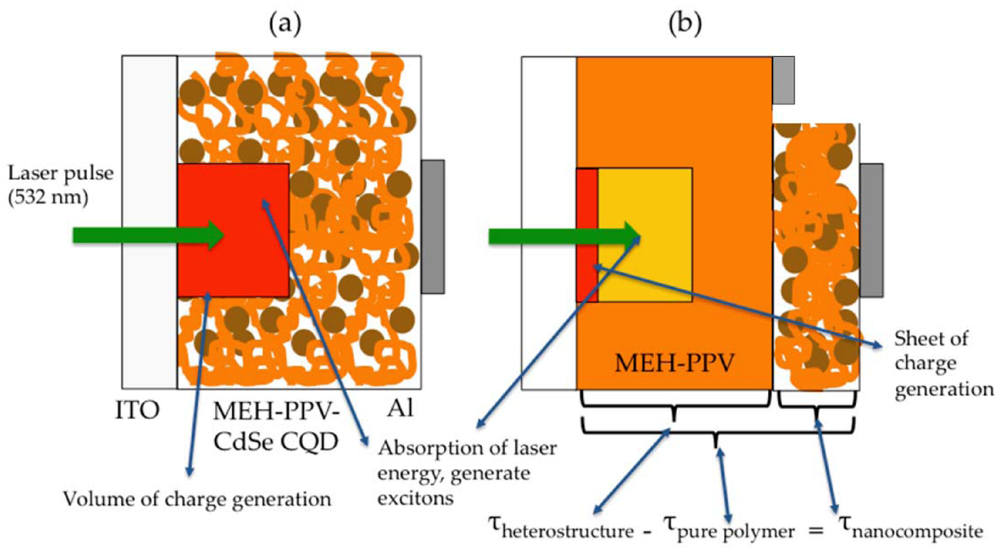
2.1. Time-of-Flight Photoconductivity Measurement of Polymer Hole Drift Mobility in MEH-PPV/CdSe Hybrid Nanocomposites

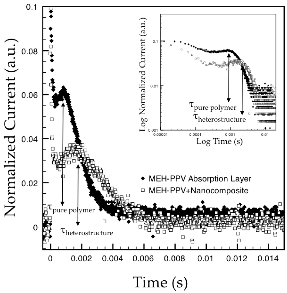
An example of the measured TOF transients for the 80:20 MEH-PPV:CdSe CQD sample (i.e., the overall heterostructure transient and the reference pure polymer transient) is shown in Figure 2. It is important to note that the appearance of the observed shoulders for all measured transients vary in shape from a plateau to a sharp shoulder. Therefore, the transit time is best defined as the roll-off point of the transient current when plotted on a log(I)-log(time) scale, as shown in the inset to Figure 2. It is also important to note that several factors must be considered for the TOF measurement to yield useful data: first, the RC time constant of the entire circuit must be significantly less than the transient decay time; second, the absorption coefficient of the active layer must be large enough such that the laser energy is absorbed in a shallow depth relative to the total thickness of the film; and third, the generated sheet of carriers must be sufficiently thin such that nearly all of the carriers arrive at the far contact (Al contact) at the same time. These factors were considered in selecting the film thickness for the measured samples, as described in the Experimental Section.
The measured transit times for the nanocomposites (τnanocomposite) are used to determine the associated hole drift mobilities according to the following equation:
Crystals 02 00078 i001
where µdrift is the hole drift mobility, d is the sample thickness, and 
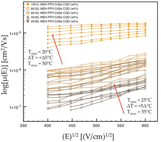
E is the applied electric field. The hole drift mobilities determined using Equation (1) for MEH-PPV-CdSe CQD nanocomposites with different concentration ratios are shown in Figure 3 as a function of the square root of the applied electric field for each measurement temperature. It is important to note that the mobility is plotted against E1/2 because it is advantageous for the disorder model analysis used to correlate mobility to internal morphology. In this figure, the general trend is that as the CdSe CQD content in the hybrid nanocomposite films increases, the hole drift mobility decreases [from ~5.9 × 10⁻⁶ cm2/Vs in MEH-PPV films to ~8.1 × 10⁻⁸ cm2/Vs in a 20:80 (wt%) MEH-PPV:CdSe CQD nanocomposite film at 25 °C and an applied field of ~2 × 10⁵ V/cm].
Figure 2. TOF transients for the entire 80:20 MEH-PPV:CdSe CQD (CdSe colloidal quantum dot) heterostructure and for the pure polymer laser absorption layer at 30 °C and an applied field of 2.6 × 10⁵ V/cm.
Crystals 02 00078 g002
Figure 3. Hole drift mobility vs. temperature and electric field for nanocomposite thin films with different MEH-PPV:CdSe CQD ratios.
Crystals 02 00078 g003

2.2. Amorphous Film Disorder Models

The measured mobility values are related to the polymer internal morphology of each film by using the BGDM and the CDM [12,13,14]. For each disorder model, it is assumed that interchain hopping conduction occurs in a polymer film when charge carriers hop between energy levels associated with two adjacent sites. According to the BGDM, the energy distribution of such hopping states is Gaussian and the energy levels of adjacent sites are uncorrelated. The primary difference in the CDM is that the energy distribution of hopping states for adjacent molecules is correlated with the spatial positions of chain sites. Each disorder model yields a corresponding energy disorder parameter, σ, which describes the energy required for a charge carrier to hop between adjacent sites in the polymer film. Therefore, smaller values of σ indicate more intimately interacting polymer chains. Specifically, according to the BGDM, the hole drift mobility in disordered materials is described by [7]:
Crystals 02 00078 i002
where T is temperature, µ is the zero-field drift mobility at T = ∞, σBGDM is the energy disorder parameter, kb is Boltzmann’s constant, Σ is the positional disorder parameter, and C is a constant, which is approximately 2.9 × 10⁻⁴ (cm/V)1/2 for MEH-PPV [12]. The positional disorder parameter, Σ, describes the fluctuation in the distance and orientation of the hopping sites associated with hopping charge carriers. Therefore, decreasing values of Σ indicate increasing film homogeneity on a sub-nanometer scale. Similarly, according to the CDM, the hole drift mobility in disordered materials is described by [8]:
Crystals 02 00078 i003
where σCDM is the energy disorder parameter,e is the charge of an electron, and a is the hopping distance between two adjacent sites. Smaller values of a also indicate more relaxed polymer chains. Thus, in order to extract information about the MEH-PPV film internal morphology from the measured hole drift mobility data, the BGDM is used to calculate the energy disorder parameter, σBGDM, and the positional disorder parameter, Σ, while the CDM is used to calculate σCDM and the hopping distance, a. By determining the disorder parameters using both models, a more complete picture of the polymer film internal morphology is obtained.

2.3. Disorder Model Parameters

It is important to note that according to Equations (2) and (3), the zero-field drift mobilities should follow the so-called non-Arrhenius temperature dependence for the BDGM and the CDM, respectively [15]:
Crystals 02 00078 i004
and
Crystals 02 00078 i005
These zero-field mobilities, µ0, are determined from the measured electric field-dependent mobilities by extrapolating the measured data to the 
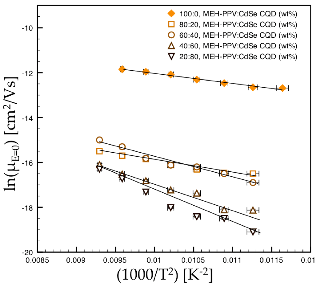
E = 0 value for each temperature and each nanocomposite concentration. The resultant plot of the non-Arrhenius temperature dependence is shown in Figure 4 for the MEH-PPV-CdSe nanocomposite films of different CQD concentration over the entire range of investigated temperatures. The energy disorder parameters for both the BGDM(σBGDM) and the CDM (σCDM) can then be obtained from the gradient of the resultant plot in accordance with Equations (4) and (5), respectively. These energy disorder parameters indicate that the average energy required for holes to hop between two adjacent sites within the MEH-PPV polymer film increases as the CdSe CQD content increases, indicating that the presence of CdSe CQDs in the nanocomposite bulk decreases interchain transport.
Figure 4. Non-Arrhenius plot of the hole drift mobility at zero-field [μ(E = 0)] as a function of inverse temperature.
Crystals 02 00078 g004
The hole drift mobility data presented in Figure 3 is also used to determine the BGDM positional disorder parameter, Σ, and the CDM hopping distance, a. In order to calculate these parameters, it is first necessary to recognize that the electric field- and temperature-dependent mobilities depicted in Figure 3 follow the Poole-Frenkel relationship [12]:
Crystals 02 00078 i006
where µ0(T) is the temperature-dependent zero-field mobility determined experimentally from Figure 3 and Y is a pre-factor corresponding to the slope of the natural log of the measured electric field-dependent mobility. Y can also be determined experimentally from Figure 3 for each temperature and each deposition technique.
In order to extract the BGDM positional disorder parameter, Σ, Equations (2) and (6) are used along with the temperature-dependent Y pre-factors from Figure 3 and the energy disorder parameters from Figure 4. The expression for the positional disorder parameter is:
Crystals 02 00078 i007
Thus, the BGDM positional disorder parameter, Σ, is determined by plotting the Υpre-factors for each temperature and nanocomposite concentration (from Figure 3) as a function of (σBGDM/kbT)2, where σBGDM is determined from Figure 4. 
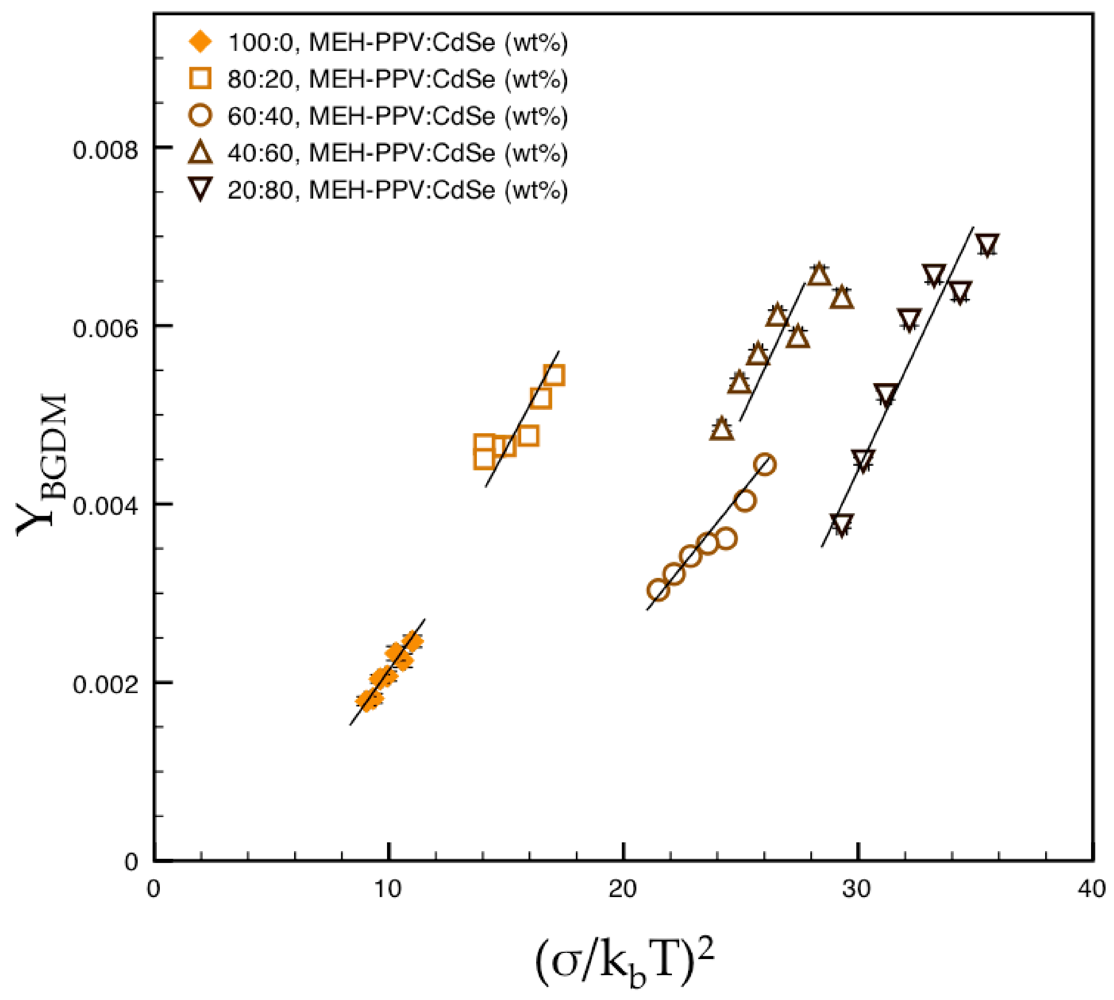
Figure 5 shows the resultant linear plots of the BDGM Υ pre-factor for the films with different MEH-PPV:CdSe ratios. The value of the x-intercept (Y = 0) for each plot is equal to Σ2. The positional disorder parameters increase as a function of increasing CdSe content in the nanocomposite, indicating an increasingly disordered state of the polymer component of the nanocomposite as more CdSe CQDs are added.
Figure 5. The Bässler’s Gaussian disorder model (BGDM) pre-factor, ΥBGDM, as a function of the second power of the energy disorder parameter normalized to kbT.
Crystals 02 00078 g005
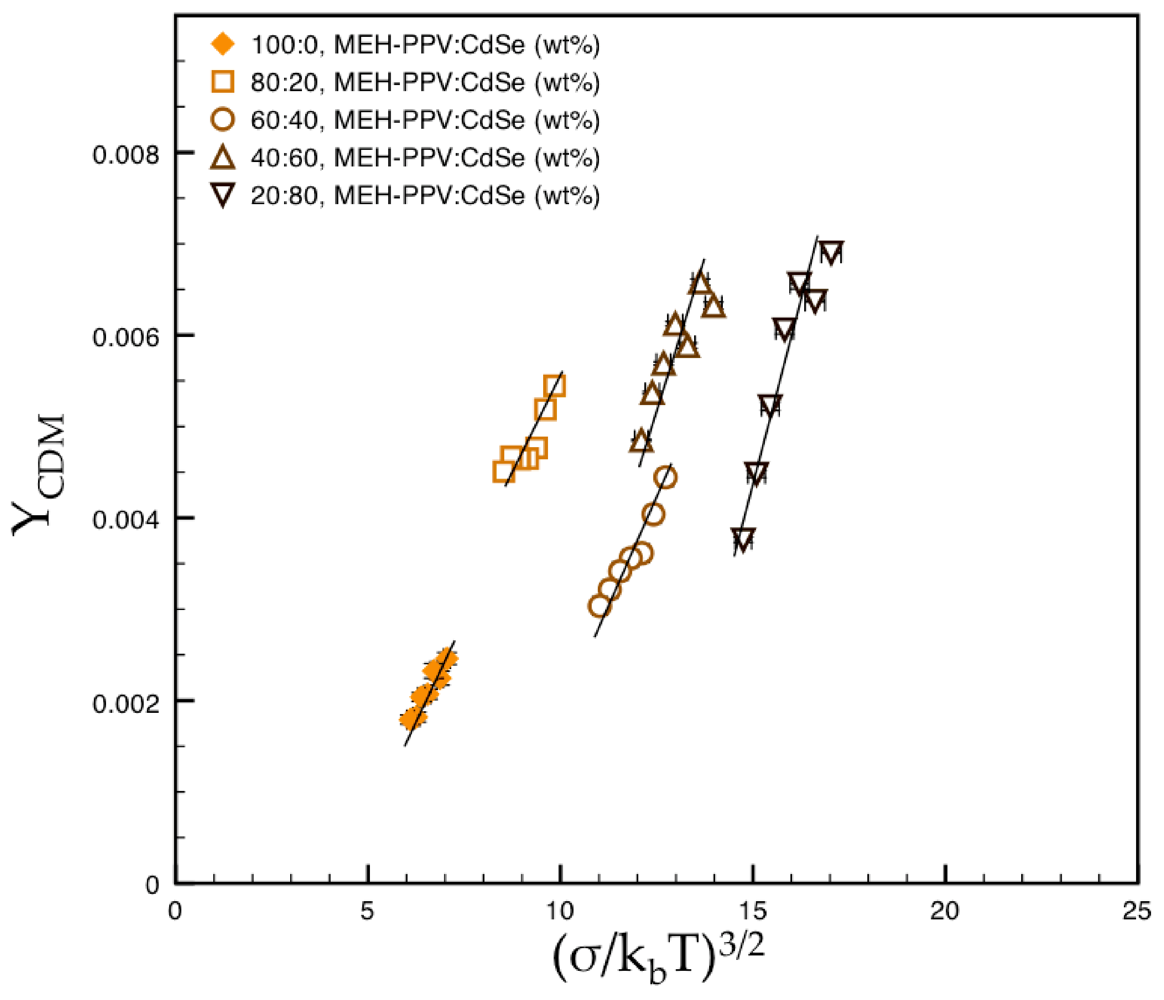
A similar procedure is used to extract the CDM hopping distance, a, the expression for which is:
Crystals 02 00078 i008
Thus, the CDM hopping distance is determined by plotting the Υpre-factorsfor each temperature and nanocomposite concentration (from Figure 3) as a function of CDM/kbT)3/2, where σCDM is determined from Figure 4. Figure 6 shows the resultant linear plots of the CDM Υ pre-factor for the pure polymer and nanocomposite samples. The value of the x-intercept (Y = 0) for each plot is equal to a. The hopping distance increases as a function of increasing CdSe CQD content, which indicates that the polymer chains are less relaxed as more CQDs are incorporated into the nanocomposites.
Figure 6. The correlated disorder model (CDM) pre-factor, ΥCDM, as a function of the 3/2-power of the energy disorder parameter normalized to kbT.
Crystals 02 00078 g006
The BGDM and CDM energy disorder parameters (σBGDM and σCDM), BGDM positional disorder parameters (Σ), and CDM hopping distances (a) extracted from the measured hole drift mobilities are summarized in Table 1. The overall picture provided by the disorder parameters in Table 1 is that increasing the incorporation of CdSe CQDs into the polymer bulk reduces interchain interaction because the polymer chains exhibit more disorder and less relaxation, and the corresponding hole hopping conduction decreases. It is important to point out that surface traps on the CQD are likely to have little influence on hole transport through the nanocomposite in this system. First, holes do not enter the CQD due to the Type-II band line-up between MEH-PPV and CdSe CQDS of this size [4]. Second, theCdSe CQDs are passivated with relatively long ligands (octadecylamine, approximately 2.2 nm in length).
Table 1. The BGDM and CDM disorder model parameters of MEH-PPV-CdSe CQD thin films with different MEH-PPV:CdSe ratios.
MEH-PPV:CdSe ratio (%)BGDM energy disorder parameter (σ, eV)CDM energy disorder parameter (σ, eV)BGDM positional disorder parameter (Σ)CDM hopping distance (a, Å)
100:00.0850.0942.644.7
80:200.1060.1183.466.3
60:400.1260.1403.748.2
40:600.1340.1494.449.5
20:800.1530.1704.9113.1
The hole drift mobility measurements for polymer-CQD nanocomposites reported herein could have important implications for the use of semiconductor nanocrystals in optoelectronic devices. It has been established that the electron percolation threshold for hopping conduction in nanocomposites is approximately 50 vol% to 65 vol% of the electron transporting material (in this case, the CdSe CQDs) relative to the polymer bulk [6]; hence, in the context of this study, a 50:50 MEH-PPV:CdSevol% ratio is approximately 15:85 MEH-PPV:CdSewt% (MEH-PPV, density of 0.98 g/cm and CdSe, density of 5.82 g/cm), which is still slightly more CdSe-rich than the maximum MEH-PPV:CdSe ratio (20:80) investigated in this TOF measurement. As a result, in order to incorporate enough CdSe CQDs into the MEH-PPV so as to achieve electron transport through the CQDs, the MEH-PPV hole transport is markedly degraded. This property of charge conduction in polymer-CQD hybrid nanocomposites is extremely relevant to the performance of optoelectronic devices (especially photovoltaics), and could be a contributing factor to the comparatively lower device performances demonstrated using these materials [2].

3. Experimental Section

MEH-PPV polymer was obtained from American Dye source (product# ADS100RE) and was used as-delivered. CdSe CQDs were obtained from NN-Labs (product# CDSE-620-25), and these CQDs range in diameter from 5.2 to 6.2 nm with an absorption band edge at 620 ± 10 nm. The MEH-PPV was dissolved in toluene (Alfa Aesar, HPLC grade) at a concentration of 1 wt%, and this solution was used for drop-cast deposition of the pure polymer scaffold. Approximately 1 mL of the 1 wt% MEH-PPV-toluene solution was directly drop-cast onto a 3.8 cm × 3.8 cm × 0.1 cm (width × length × height) indium-tin-oxide (ITO)-coated float-glass substrate (Delta Technologies) and allowed to dry in a toluene-rich atmosphere to a final film thickness of 5.5 ± 0.1 µm. Next, MEH-PPV-CdSe CQD hybrid nanocomposite thin films were deposited by emulsion RIR-MAPLE [10,11,16] using the sequential deposition technique [17]. MEH-PPV:CdSe CQD wt% ratios of 80:20, 60:40, 40:60, and 20:80 were deposited for final film thickness of 6.5 ± 0.15 µm (the nanocomposite layer thickness for each dot concentration ratio was approximately 1.0 ± 0.05 µm). This final film thickness was selected for the TOF measurements because it results in a low RC time constant in the polymer film so as to enable a fast charge decay, it guarantees that all of the applied voltage is dropped across the film under measurement, and it ensures that the resultant TOF transients can be clearly discerned and measured. It is important to note that the drop-cast deposition of the pure polymer scaffold for each nanocomposite sample enables the generation of sheet charge for each sample and provides a reference polymer mobility measurement for each sample. Drop-cast deposition was used for these scaffolds in order to increase sample throughput and emulsion-based RIR-MAPLE deposition was used for the nanocomposite deposition because of the similar solubility of the constituent materials. A film of MEH-PPV only was deposited by emulsion-based RIR-MAPLE onto an ITO-coated glass substrate to a final thickness of 6.5 ± 0.1 µm in order to compare the measured mobility of polymer and nanocomposite films.
The deposited heterostructures were characterized by the TOF photoconductivity method [13] to measure hole drift mobility. A nanosecond Nd:YAG pulsed laser at 532 nm was directed normally onto a device consisting of a transparent top contact (indium tin oxide—ITO), the film under measurement (MEH-PPV or the MEH-PPV-CdSe CQD nanocomposite), and a bottom ohmic contact (aluminum). For the nanocomposite samples, separate bottom contacts for the reference MEH-PPV scaffolds were also deposited. The 532 nm laser line was chosen because it is readily absorbed by MEH-PPV. Photogenerated excitons are dissociated at the interface of the active layer and the transparent contact such that electrons are immediately collected by the ITO electrode. An applied voltage bias was provided using a Keithley E3612A power supply in order to create an electric field that sweeps holes to the aluminum contact. The collected holes produce a transient photocurrent that was measured across a 100-kΩ resistor using a Tektronix 2024 200-MHz oscilloscope. For the TOF measurements, the film temperature for each device was maintained using an ITO substrate heater. The measurement temperatures for the pure MEH-PPV film was varied from 20 °C to 50 °C in increments of 5 °C, and the measurement temperatures for the nanocomposite heterostructure devices were varied from 25 °C to 55 °C in increments of 5 °C.

4. Conclusions

MEH-PPV:CdSe hybrid nanocomposite thin films with different CQD concentrations are investigated using a modified TOF technique enabled by RIR-MAPLE deposition. These measurements demonstrate that the hole drift mobilities in MEH-PPV:CdSe nanocomposites decrease as a function of increasing CdSeCQD concentration in the polymer bulk. Moreover, analysis using amorphous film disorder models indicates that the decreased hole drift mobilities derive from disrupted interchain interaction in the MEH-PPV bulk, as evidenced by higher BGDM and CDM energy disorder parameters, larger BGDM positional disorder parameters, and longer CDM hopping distances. The impact of reduced polymer interchain interaction is important because the CQD concentration necessary to establish electron percolation through CQD networks significantly degrades hole transport in the polymer bulk. Better understanding of this property of charge conduction in polymer-CQD hybrid nanocomposites is valuable to optimizing the performance of future optoelectronic devices.

Acknowledgments

This work was supported by the Office of Naval Research under Grant N00014-10-1-0481. The authors would also like to thank Tuan Vo-Dinh, Jon Scaffidi, and Richard A. Palmer, all of Duke University, for their kind assistance in the performance of these experiments.

References and Notes

  1. Sirringhaus, H.; Tessler, N.; Friend, R.H. Integrated optoelectronic devices based on conjugated polymers. Science 1998, 280, 1741–1744. [Google Scholar]
  2. Günes, S.; Neugebauer, H.; Sariciftci, N.S. Conjugated polymer-based organic solar cells. Chem. Rev. 2007, 107, 1324–1338. [Google Scholar]
  3. McDonald, S.A.; Konstantatos, G.; Zhang, S.; Cyr, P.W.; Klem, E.J.D.; Levina, L.; Sargent, E.H. Solution-processed pbs quantum dot infrared photodetectors and photovoltaics. Nat. Mater. 2005, 4, 138–142. [Google Scholar]
  4. Stiff-Roberts, A.D.; Lantz, K.R.; Pate, R. Room-temperature, mid-infrared photodetection in colloidal quantum dot/conjugated polymer hybrid nanocomposites: A new approach to quantum dot infrared photodetectors. J. Phys. D: Appl. Phys. 2009, 42, 234004. [Google Scholar] [CrossRef]
  5. Tang, J.; Sargent, E.H. Infrared colloidal quantum dots for photovoltaics: Fundamentals and recent progress. Adv. Mater. 2010, 23, 12–29. [Google Scholar]
  6. Greenham, N.C.; Peng, X.; Alivisatos, A.P. Charge separation and transport in conjugated-polymer/semiconductor-nanocrystal composites studied by photoluminescence quenching and photoconductivity. Phys. Rev. B 1996, 54, 17628–17637. [Google Scholar] [CrossRef]
  7. Bässler, H. Charage transport in disordered organic photoconductors. Phys. Status Solidi 1993, 175, 15–56. [Google Scholar] [CrossRef]
  8. Parris, P.E.; Kenkre, V.M.; Dunlap, D.H. Nature of charge carriers in disordered molecular solids: Are polarons compatible with observations? Phys. Rev. Lett. 2001, 87, 126601. [Google Scholar]
  9. Pate, R.; McCormick, R.; Chen, L.; Zhou, W.; Stiff-Roberts, A.D. Rir-maple deposition of conjugated polymers for application to optoelectronic devices. Appl. Phys. A: Mater. Sci. Proc. 2011, 105, 555–563. [Google Scholar] [CrossRef]
  10. Pate, R.; Stiff-Roberts, A.D. The impact of laser-target absorption depth on the surface and internal morphology of matrix-assisted pulsed laser evaporated conjugated polymer thin films. Chem. Phys. Lett. 2009, 477, 406–410. [Google Scholar] [CrossRef]
  11. Pate, R.; Lantz, K.R.; Stiff-Roberts, A.D. Tabletop resonant infrared matrix assisted pulsed laser evaporation of light emitting organic thin films. IEEE J. Quantum. Elect. 2008, 14, 1022–1030. [Google Scholar]
  12. Inigo, A.R.; Chang, C.C.; Fann, W.; White, J.D.; Huang, Y.S.; Jeng, U.S.; Sheu, H.S.; Peng, K.Y.; Chen, S.A. Enhanced hole mobility in poly-(2-methoxy-5-(2-ethylhexoxy)-1,4-phenylenevinylene) by elimination of nanometer-sized domains. Adv. Mater. 2005, 17, 1835–1838. [Google Scholar]
  13. Inigo, A.R.; Chiu, H.C.; Fann, W.; Huang, Y.S.; Jeng, U.S.; Lin, T.S.; Hsu, C.H.; Peng, K.Y.; Chen, S.A. Disorder controlled hole transport in meh-ppv. Phys. Rev. B 2004, 69, 075201. [Google Scholar]
  14. Inigo, A.R.; Huang, Y.F.; White, J.D.; Huang, Y.S.; Fann, W.S.; Peng, K.Y.; Chen, S.A. Review of morphology dependent charge carrier mobility in meh-ppv. J. Chin. Chem. Soc. 2010, 57, 459–468. [Google Scholar]
  15. Khan, R.U.A.; Poplavskyy, D.; Kreouzis, T.; Bradley, D.D.C. Hole mobility within arylamine-containing polyflourene copolymers: A time-of-flight transient-photocurrent study. Phys. Rev. B 2007, 75, 035215. [Google Scholar]
  16. Pate, R.; Lantz, K.R.; Dhawan, A.; Vo-Dinh, T.; Stiff-Roberts, A.D. Resonant infrared matrix-assisted pulsed laser evaporation of inorganic nanoparticles and organic/inorganic hybrid nanocomposites. In Proceedings of International Symposium on High Power Laser Ablation, Santa Fe, NM, USA, April 2010; AIP Conference Proceedings: Melville, NY, USA, 2010; 1278, pp. 813–823. [Google Scholar]
  17. Pate, R.; Lantz, K.R.; Stiff-Roberts, A.D. Resonant infrared matrix-assisted pulsed laser evaporation of cdse colloidal quantum dot/poly[2-methoxy-5-(2'-ethylhexyloxy)-1,4-(1-cyano vinylene)phenylene] hybrid nanocomposite thin films. Thin Solid Films 2009, 517, 6798–6802. [Google Scholar]

