Electromagnetically Induced Transparency (EIT) Like Transmission Based on 3 × 3 Cascaded Multimode Interference Resonators

International School (VNU-IS), Vietnam National University (VNU), Hanoi 1000, Vietnam
Micromachines 2018, 9(8), 417; https://doi.org/10.3390/mi9080417
Submission received: 1 July 2018
/
Revised: 27 July 2018
/
Accepted: 1 August 2018
/
Published: 20 August 2018
(This article belongs to the Special Issue Micro-Resonators: The Quest for Superior Performance)
Abstract
:We propose a method for generating the electromagnetically induced transparency (EIT) like-transmission by using microring resonator based on cascaded 3 × 3 multimode interference (MMI) structures. Based on the Fano resonance unit created from a 3 × 3 MMI coupler with a feedback waveguide, two schemes of two coupled Fano resonator unit (FRU) are investigated to generate the EIT like transmission. The theoretical and numerical analysis based on the coupled mode theory and transfer matrix is used for the designs. Our proposed structure has advantages of compactness and ease of fabrication. We use silicon waveguide for the design of the whole device so it is compatible with the existing Complementary Metal-Oxide-Semiconductor (CMOS) circuitry foundry. The fabrication tolerance and design parameters are also investigated in this study.
1. Introduction
The electromagnetically induced transparency (EIT) effect is a nonlinear effect found in the interaction process between light and material. The EIT effect has been intensively investigated in recent years [1,2]. The EIT has wide applications such as in quantum information [3], lasing without inversion [4], optical delay, slow light [5], nonlinearity enhancement [6] and precise spectroscopy [7], pushing frontiers in quantum mechanics and photonics and sensing technology [8]. In order to create the EIT effect, there are some suggested approaches.
There is a significant benefit to determine the optical EIT like transmissions with high modulation depth, which is defined by the difference in intensities between the peak and the dip at resonant wavelengths. The EIT was first observed in atomic media [2]. Then, the EIT-like effects were found in optical coupled resonant systems [9,10,11], mechanics, electrical circuits [12], plasmonics, metamaterials [7,13] and hybrid configurations [14]. In the coupled resonant systems, the basic underlying physical principle is the interference of fields instead of the probability of amplitudes, as in a three-level atomic system [15,16]. Most of the proposed structures so far for the optical EIT generation use metal-insulator-metal (MIM) plasmonic waveguide resonators [17,18], array of fiber optic resonators [19], microspheres [20], metallic arrays of asymmetric dual stripes [21], heptamer-hole array [22], plasmonic nanoring pentamers [23] and microtoroid resonator coupled system [24]. For these systems, the fiber beam splitters, directional couplers or MIM plasmonic waveguide must be used. As a result, such structures bring large size, the complexity of the fabrication process to control exactly the coupling ratios of the directional couplers and sensitivity to fabrication tolerance.
The transparency window of the EIT is caused by reduced absorption, due to the quantum destructive interference between the transitions from the two dressed states, into a common energy level. Similarly, the EIT-like effect generated by optical resonators work by the means of coherent interference between the resonating modes which produce optical transparency inside the absorption window [25]. Compared to the EIT in atomic systems, the analogue of electromagnetically induced transparency with optical resonators based on directional couplers has many remarkable advantages such as simpler structure, smaller device size and easier design. However, due to the small size of these structures, it is challenging to detune optical resonator for controlling the resonant interaction between the two optical pathways and controlling the coupling ratio of the directional couplers [26].
In the literature, only 2 × 2 directional coupler was used for microring resonator based on the EIT effects [25]. However, such structure is very sensitive to the fabrication. It has a large size and requires a complicated fabrication process. It was shown that the integration of multimode interference (MMI) and resonators can provide new physical characteristics. By using the MMIs, we can overcome the disadvantages of devices based on directional couplers such as compactness, ease of fabrication and large fabrication tolerance [27]. One of such structures is a 3 × 3 MMI based microring resonator. We have proposed for the first time microring resonator structures based on 3 × 3 and 4 × 4 MMI couplers for Fano resonance generation [28,29,30]. In this study, we further develop new structures based on only cascaded 3 × 3 multimode interference coupler based microring resonators to produce the EIT resonance like transmissions. The proposed device is analyzed and optimized using the transfer matrix method, the beam propagation method (BPM) and finite difference time difference (FDTD) [31]. A description of the theory behind the use of multimode structures to achieve the FRU and EIT effect is presented in Section 2 and Section 3. A brief summary of the results of this research is given in Section 4.
2. Single Fano Resonance Unit (FRU)
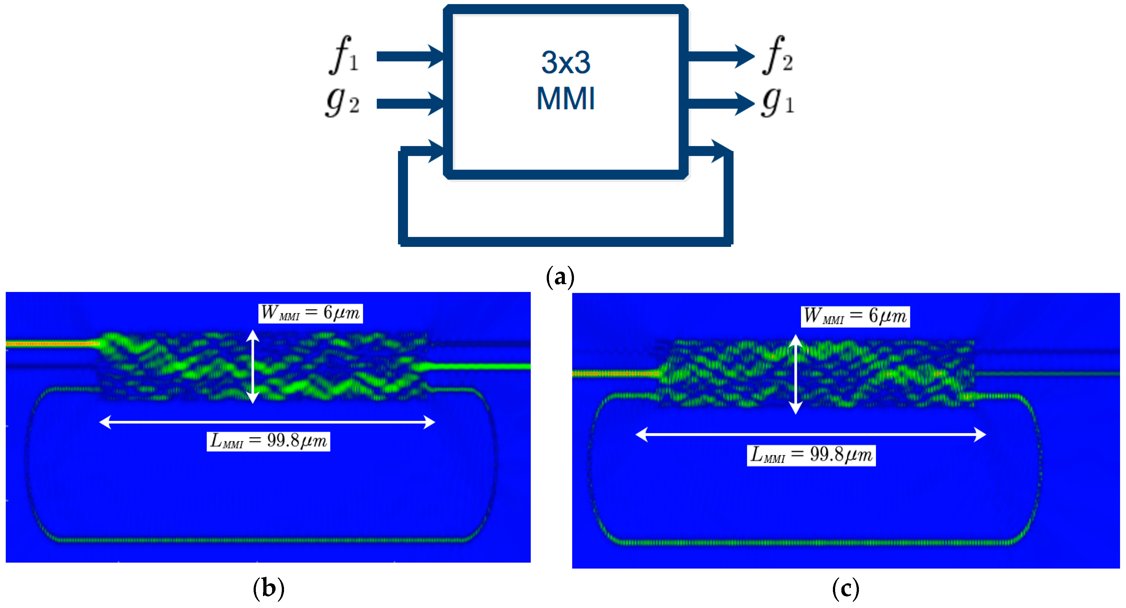
Fano resonance can be created by many approaches such as integrated waveguide-coupled microcavities [32,33], prism-coupled square micro-pillar resonators, multimode tapered fiber coupled micro-spheres and Mach Zehnder interferometer (MZI) coupled micro-cavities [34], plasmonic waveguide structure [35,36]. We have proposed integrated photonic circuits for realizing Fano resonance based on 3 × 3 MMI and 4 × 4 MMI microring resonator [29,37]. Figure 1a shows a scheme for Fano resonance unit (FRU) based on only one 3 × 3 MMI coupler with a feedback waveguide. Figure 1b,c shows the FDTD simulation for the FRU with input signal presented at input ports 1 and 2, respectively.
In the time domain, the Fano resonance system created by 3 × 3 MMI coupler based microring resonator in Figure 1 can be expressed by the coupled mode equations [38]
where n = 1, 2 and ; is the phase of the resonator depending on the feedback waveguide, is the nonlinear phase shift, is the amplitude in the resonator mode; , are the complex amplitudes at input and output ports; and are resonant frequency and lifetime of the resonator.
In the frequency domain, the 3 × 3 MMI coupler can be described by a transfer matrix which describes the relationships between the input and output complex amplitudes (fields) of the coupler [39]. The length of the MMI coupler is to be , is the beat length of the MMI coupler. The relationship between the output complex amplitudes and the input complex amplitudes of the coupler can be expressed by [39]
The complex amplitudes at output ports 1 and 2 of the first microring resonator of Figure 1 are given by
where is the transmission loss along the ring waveguide, L is the length of the feedback waveguide and (dB/cm) is the loss coefficient in the core of the optical waveguide; is the phase accumulated over the racetrack waveguide, where and is the effective refractive index, is the wavelength.
In this study, we use silicon waveguide for the design, where ( = 1.46) is used as the upper cladding material. The parameters used in the designs are as follows: the waveguide has a standard silicon thickness of and access waveguide widths are for single mode operation. It is assumed that the designs are for the transverse electric (TE) polarization at a central optical wavelength . In this study, we use the three dimensional beam propagation method (3D-BPM) and Finite Difference Time Domain (FDTD) to design the whole structure [40].
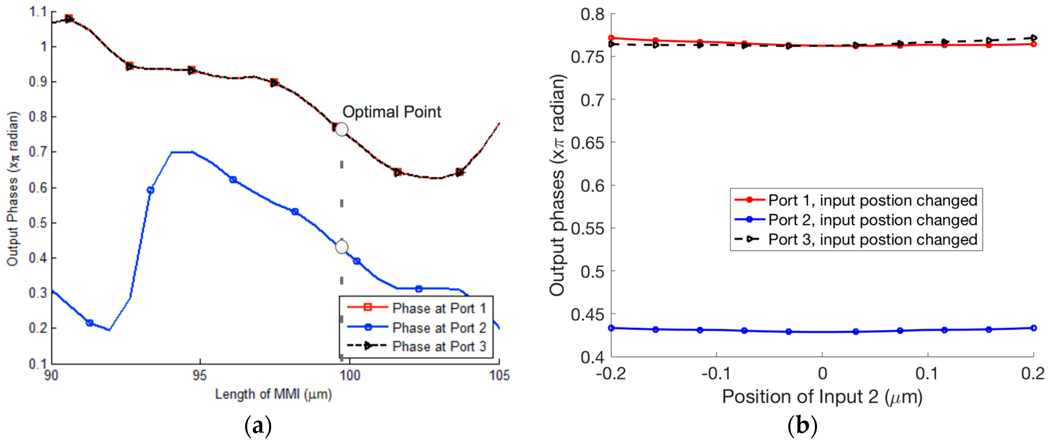
Firstly, we optimize the position of the access waveguide ports of the 3 × 3 MMI coupler to determine the proper matrix of the 3 × 3 MMI coupler expressed by Equation (3). The normalized output powers at output ports of the 3 × 3 MMI varying with the location of input port 1 are shown in Figure 2a. Figure 2b shows the normalized output powers at output ports for different locations of input port 2. Here, the width and length of the MMI coupler are optimized by the BPM simulations to be . As a result, the optimal positions of the input ports 1 and 3 are , respectively.
The phase sensitivity of the output signals to the length variation of the 3 × 3 MMI coupler based microring resonators is particularly important to device performance. We use the BPM to investigate the effect of the MMI length on the phase sensitivity. Figure 3a shows the phases at output ports of the 3 × 3 MMI coupler at different MMI lengths. We see that a change of ±10 nm in MMI length causes a change of 4.7 × 10⁻⁴ π (rad) in output phases. For the existing CMOS circuitry with a fabrication error of ±5 nm [41], this is feasible and has a very large fabrication tolerance. Similarly, we consider the effect of the positions of input waveguides on the phase sensitivity as shown in Figure 3b. For a fabrication tolerance in the MMI length of ±50 nm, the fluctuation in phases is nearly unchanged.
3. Coupled Fano Resonances and Generation of the EIT Effect
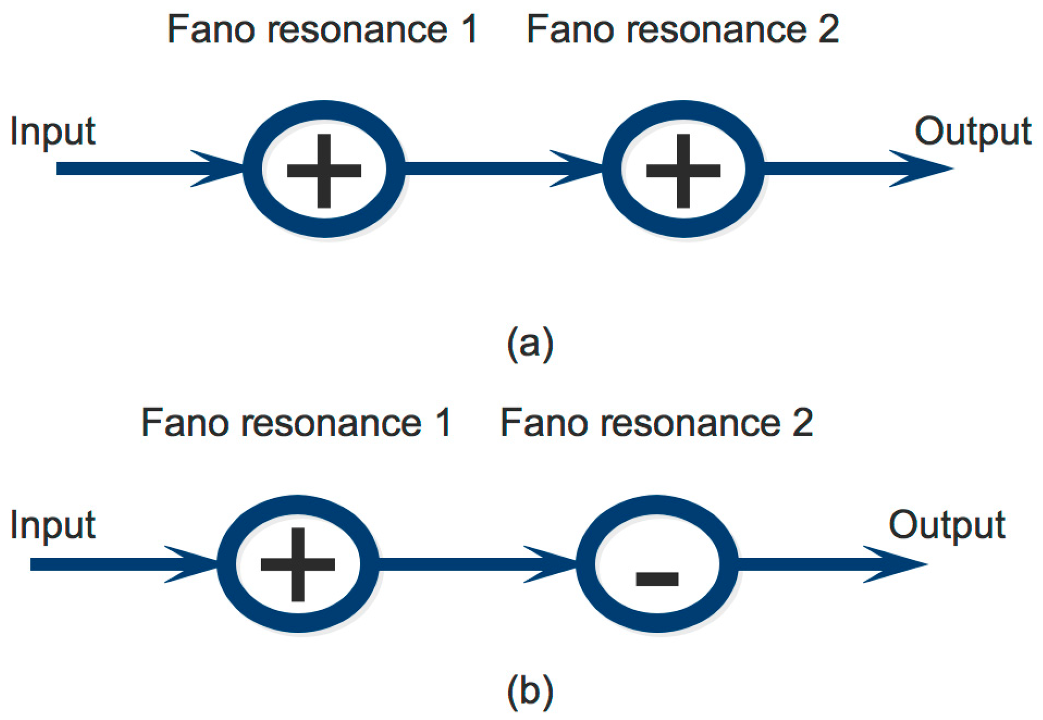
The schemes for coupled Fano resonances to generate the EIT effect is modeled in Figure 4, where single Fano resonance 1 and Fano resonance 2 of Figure 4a is exactly the same and Fano resonance 1 and Fano resonance 2 of Figure 4b is different with an exchange of input ports. We show that by cascading two Fano resonances as shown in Figure 4, the EIT effects can be created. The exchange unit can be realized by using only one 2 × 2 MMI coupler as shown in reference [42].
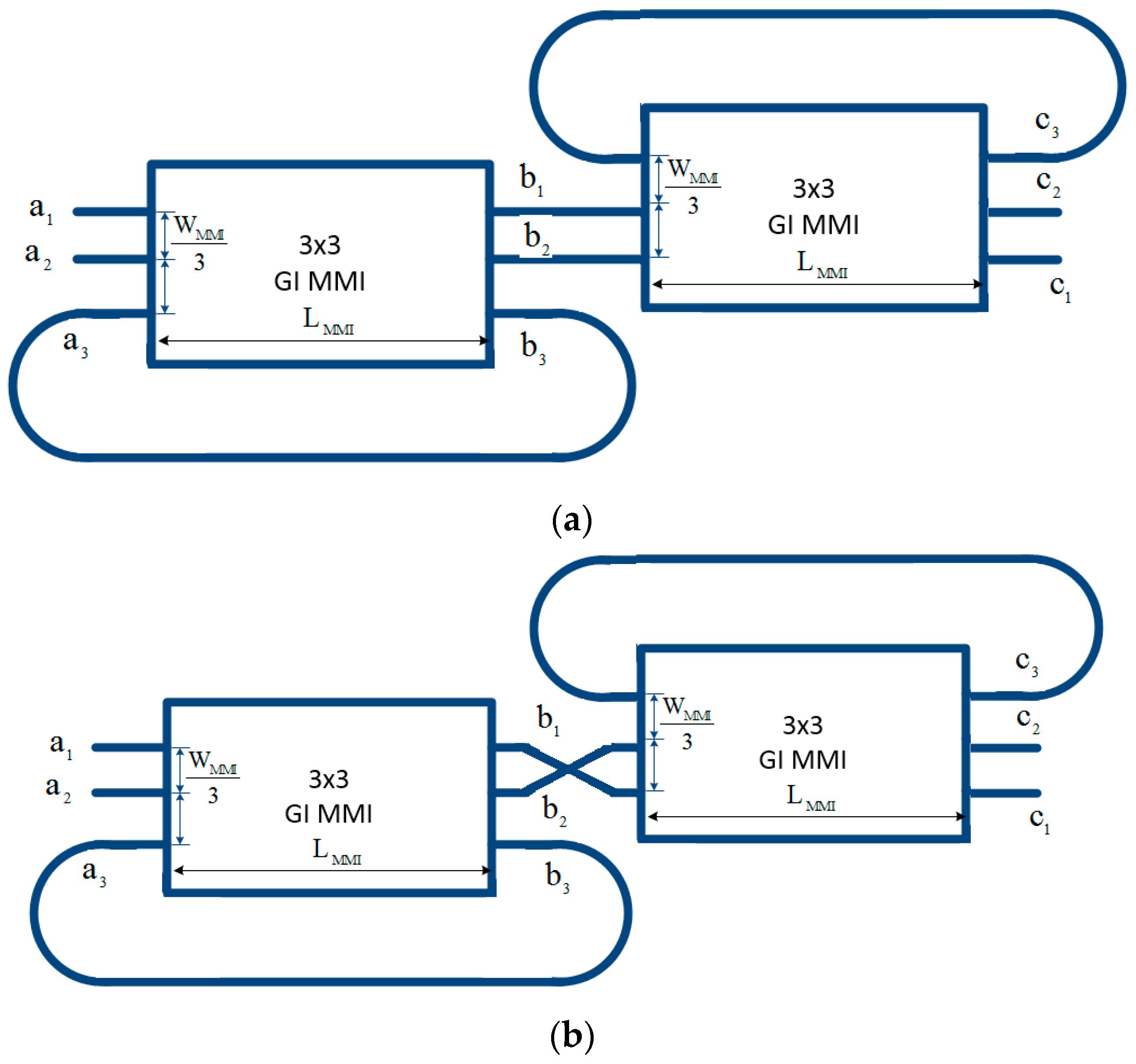
In our case, the Fano resonance 1 and 2 are the FRU created by 3 × 3 MMI coupler based microring resonator as shown in Figure 1. The first schemes of Figure 4a can be made as shown in Figure 5a and the second scheme of Figure 4b can be made as shown in Figure 5b.
By using analytical analysis, the transmissions at the output ports of Figure 5a, for the input signal presented at input port 1 () are expressed by
The transmissions at these output ports of Figure 5b, for the input signal presented at input port 1 () are
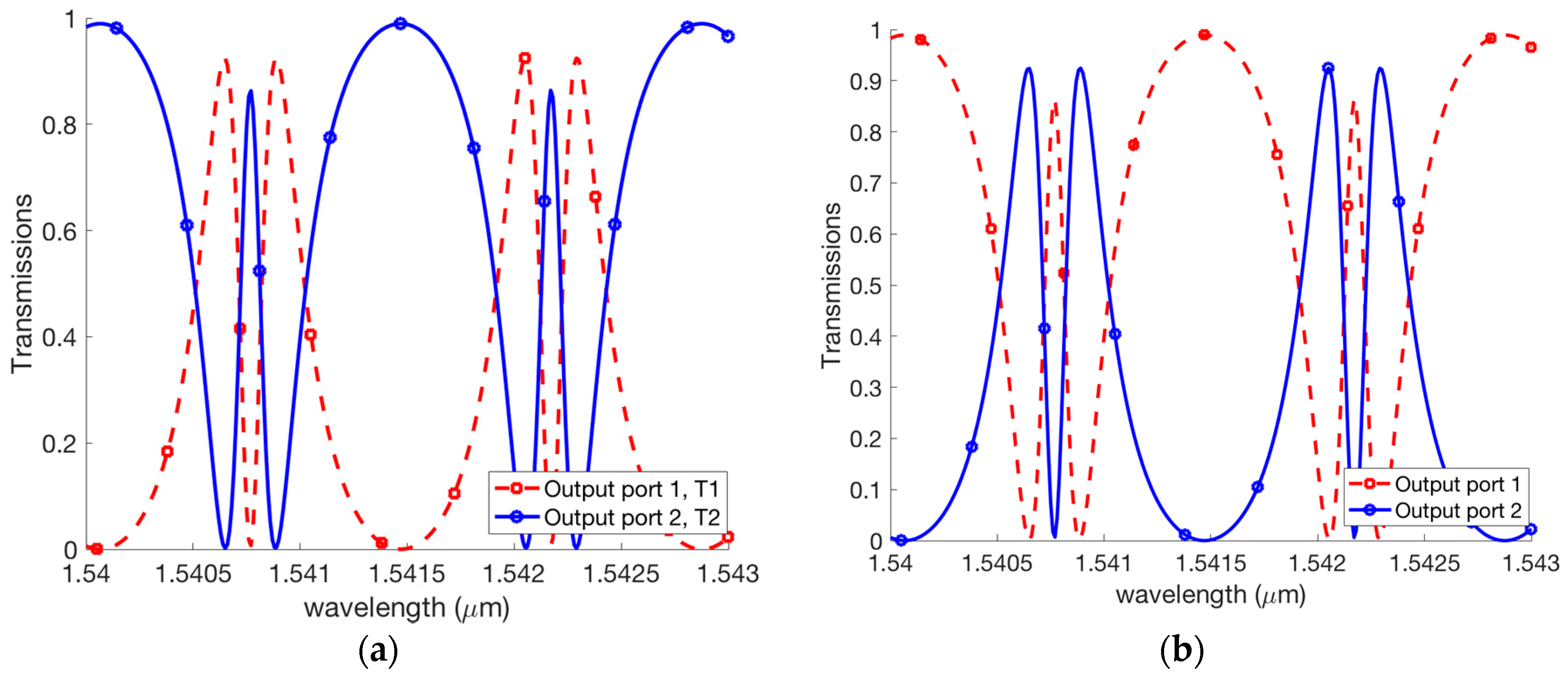
For our design, the silicon waveguide is used. The effective refractive index calculated by the FDM (Finite Difference Method) is to be for the TE polarization. It assumed that the loss coefficient of the silicon waveguide is [43], the length of the feedback waveguide is [25]. For the first scheme of Figure 5a, the EIT effects shown in Figure 6a can be generated at output ports 1 and 2 while the input signal is at the input port 1. Figure 6b shows the EIT effects are also created at output ports 1 and 2 while the input signal is presented at input port 2. We see that the modulation depth of 80% for these EIT like transmissions have been achieved. As a result, our structure can generate both the W-shape and M-shape transmissions. Such shapes can be useful for optical switching, fast and slow light and sensing applications.
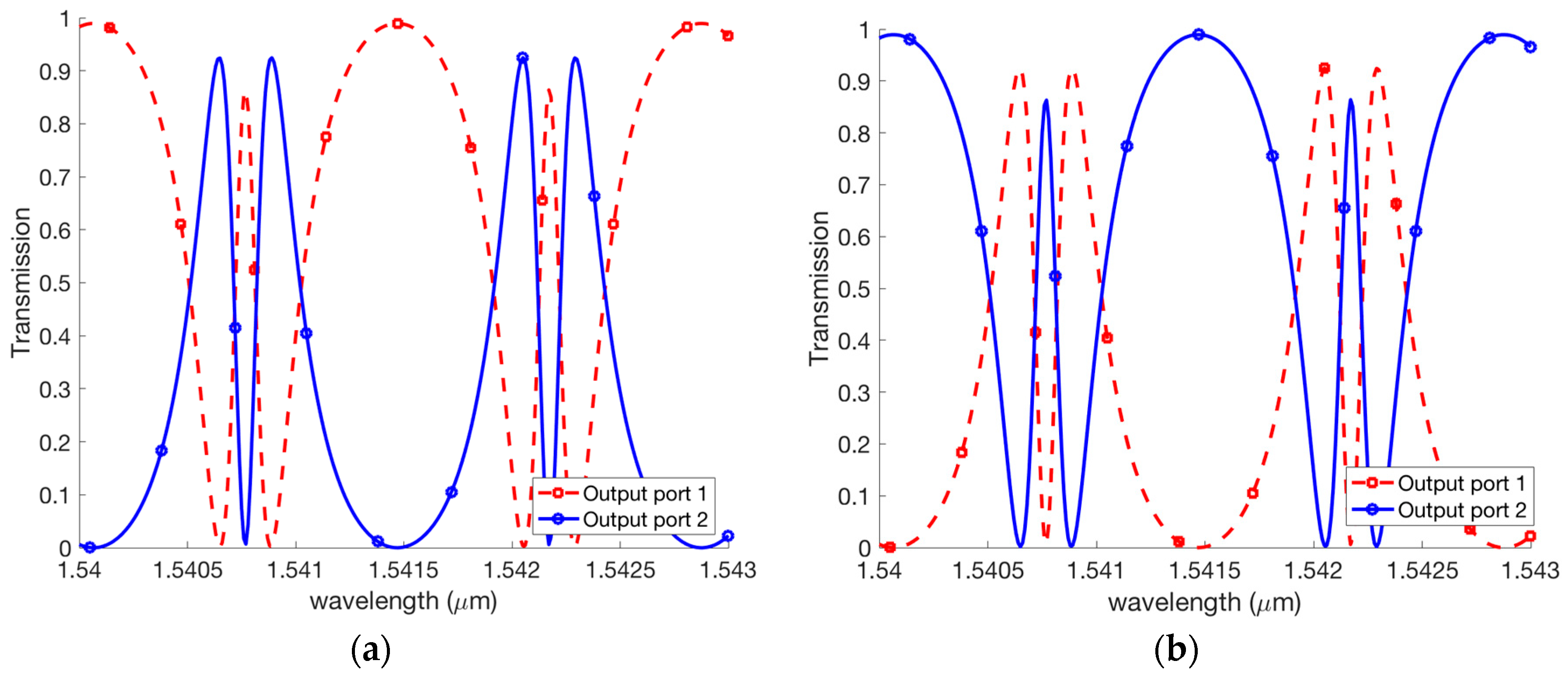
For the second scheme of Figure 5b, the EIT effects shown in Figure 7a can be generated at output port 1 and port 2 while input signal is at input port 1. Figure 7b shows the EIT effects are also created at output ports 1 and 2 while the input signal is presented at input port 2.
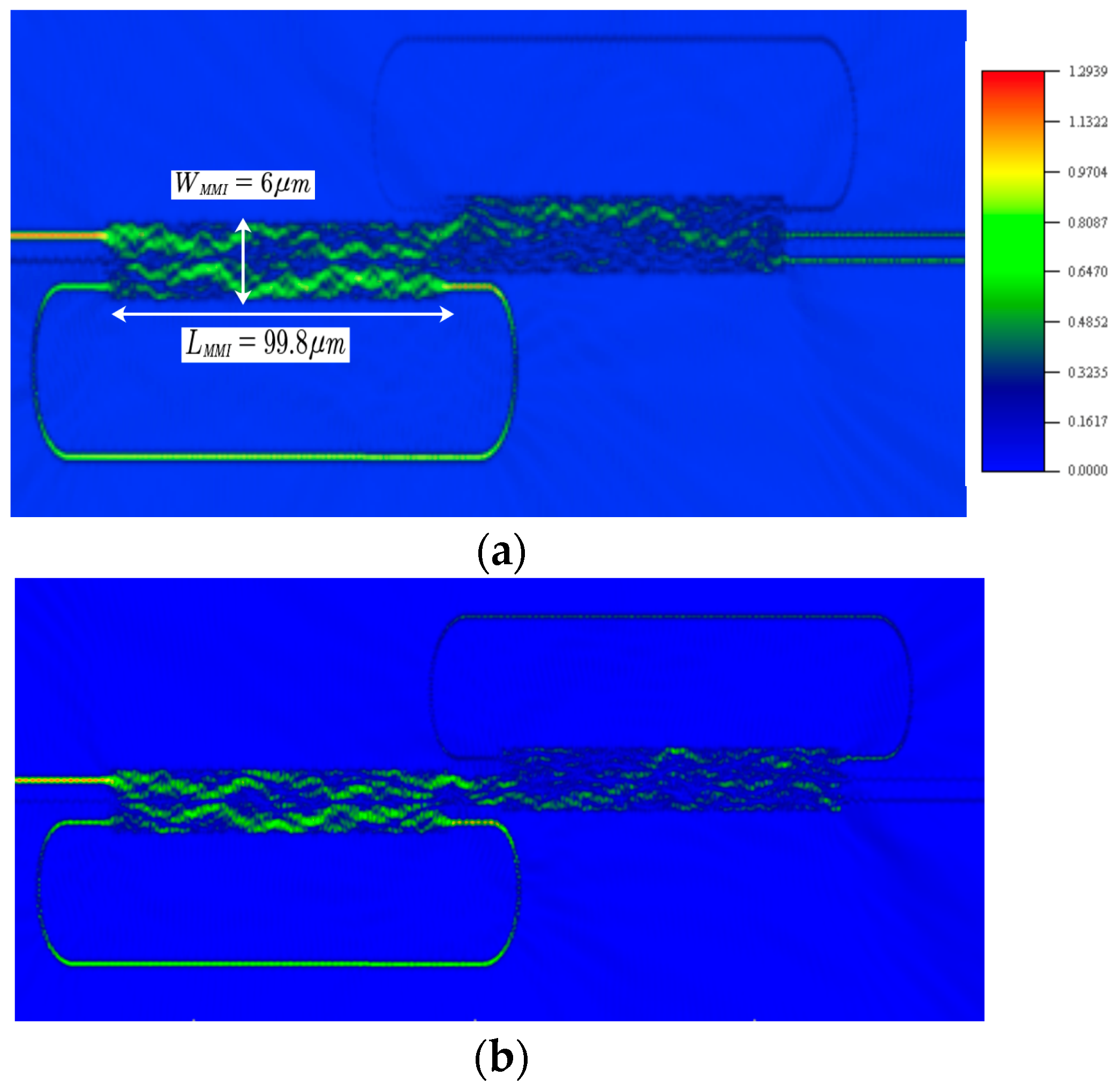
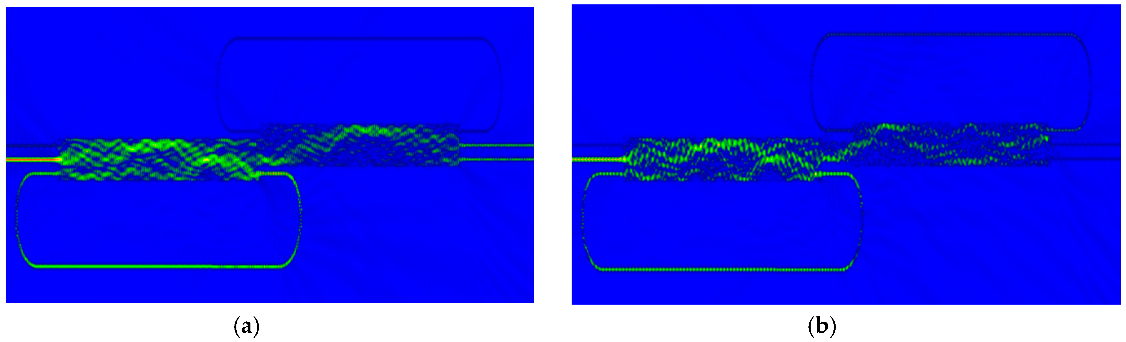
In order to verify our proposed analytical theory, we use the FDTD for accurate predictions of the device’s working principle. Figure 8 shows the FDTD simulations for the device of Figure 5a,b for input signal at port 1, respectively. Figure 9 shows the FDTD of Figure 5a,b for input signal at port 2. In our FDTD simulations, we take into account of the refractive index of silicon material calculated by using the Sellmeier equation [44,45]:
where and .
In our FDTD simulations, a Gaussian light pulse of 15 fs pulse width is launched from the input to investigate the transmission characteristics of the device. The grid sizes and are chosen [46].
For the purpose of comparing the theoretical and FDTD analysis, we investigate a comparison of the EIT like transmission effect between the theory and FDTD simulations. It is shown that the FDTD simulation has a good agreement with our theoretical analysis as presented in Figure 10.
4. Conclusions
We have presented a new method for the generation of the EIT effect based on coupled 3 × 3 MMI based microring resonators. Both of the M-shape and W-shape like transmissions are created. The device based on silicon waveguide, that is compatible with the existing CMOS circuitry, has been optimally designed. Our FDTD simulations show a good agreement with the theoretical analysis based on the transfer matrix method. The EIT effect can be determined based on these structures with advantages of ease of fabrication and large fabrication tolerance.
Funding
This research is funded by Ministry of Natural Resources and Environment of Vietnam under the project BĐKH.30/16-20.
Conflicts of Interest
The author declares no conflict of interest.
References
- Zhou, X.; Zhang, L.; Pang, W.; Zhang, H.; Yang, Q.; Zhang, D. Phase characteristics of an electromagnetically induced transparency analogue in coupled resonant systems. New J. Phys. 2013, 15, 103033. [Google Scholar] [CrossRef] [Green Version]
- Fleischhauer, M.; Imamoglu, A.; Marangos, J.P. Electromagnetically induced transparency: Optics in coherent media. Rev. Mod. Phys. 2005, 77, 633–673. [Google Scholar] [CrossRef] [Green Version]
- Lvovsky, A.I.; Sanders, B.C.; Tittel, W. Optical quantum memory. Nat. Photonics 2009, 3, 706–714. [Google Scholar] [CrossRef]
- Harris, S.E. Lasers without inversion: Interference of lifetime-broadened resonances. Phys. Rev. Lett. 1989, 62, 1033–1036. [Google Scholar] [CrossRef] [PubMed]
- Chin, S.; Thévenaz, L. Tunable photonic delay lines in optical fibers. Laser Photonics Rev. 2012, 6, 724–738. [Google Scholar] [CrossRef] [Green Version]
- Tanji-Suzuki, H.; Chen, W.; Landig, R.; Simon, J.; Vuletić, V. Vacuum-induced transparency. Science 2011, 361. [Google Scholar] [CrossRef]
- Tassin, P.; Zhang, L.; Zhao, R.; Jain, A.; Koschny, T.; Soukoulis, C.M. Electromagnetically induced transparency and absorption in metamaterials: The radiating two-oscillator model and its experimental confirmation. Phys. Rev. Lett. 2012, 109, 187401. [Google Scholar] [CrossRef] [PubMed]
- Wu, D.; Liu, Y.; Yu, L.; Yu, Z.; Chen, L.; Li, R.; Ma, R.; Liu, C.; Zhang, J.; Ye, H. Plasmonic metamaterial for electromagnetically induced transparency analogue and ultra-high figure of merit sensor. Sci. Rep. 2017, 7, 45210. [Google Scholar] [CrossRef] [PubMed]
- Totsuka, K.; Kobayashi, N.; Tomita, M. Slow light in coupled-resonator-induced transparency. Phys. Rev. Lett. 2007, 98, 213904. [Google Scholar] [CrossRef] [PubMed]
- Chremmos, I.; Schwelb, O. Photonic Microresonator Research and Applications; Springer: New York, NY, USA, 2010. [Google Scholar]
- Xu, Q.; Sandhu, S.; Povinelli, M.L.; Shakya, J.; Fan, S.; Lipson, M. Experimental realization of an on-chip all-optical analogue to electromagnetically induced transparency. Phys. Rev. Lett. 2006, 96, 123901. [Google Scholar] [CrossRef] [PubMed]
- Garrido Alzar, C.L.; Martinez, M.A.G.; Nussenzveig, P. Classical analog of electromagnetically induced transparency. Am. J. Phys. 2002, 70, 37–41. [Google Scholar] [CrossRef] [Green Version]
- Liu, N.; Langguth, L.; Weiss, T.; Kästel, J.; Fleischhauer, M.; Pfau, T.; Giessen, H. Plasmonic analogue of electromagnetically induced transparency at the drude damping limit. Nat. Mater. 2009, 8, 758–762. [Google Scholar] [CrossRef] [PubMed]
- Weis, P.; Garcia-Pomar, J.L.; Beigang, R.; Rahm, M. Hybridization induced transparency in composites of metamaterials and atomic media. Opt. Express 2011, 19, 23573–23580. [Google Scholar] [CrossRef] [PubMed]
- Smith, D.D.; Chang, H.; Fuller, K.A.; Rosenberger, A.T.; Boyd, R.W. Coupled-resonator-induced transparency. Phys. Rev. A 2004, 69, 063804. [Google Scholar] [CrossRef]
- Peng, B.; Özdemir, Ş.K.; Chen, W.; Nori, F.; Yang, L. What is and what is not electromagnetically induced transparency in whispering-gallery microcavities. Nat. Commun. 2014, 5, 5082. [Google Scholar] [CrossRef] [PubMed] [Green Version]
- Chen, Z.; Song, X.; Duan, G.; Wang, L.; Yu, L. Multiple fano resonances control in mim side-coupled cavities systems. IEEE Photonics J. 2015, 7, 1–5. [Google Scholar] [CrossRef]
- Wang, Y.; Li, S.; Zhang, Y.; Yu, L. Independently formed multiple fano resonances for ultra-high sensitivity plasmonic nanosensor. Plasmonics 2018, 13, 107–113. [Google Scholar] [CrossRef]
- Li, J.; Qu, Y.; Wu, Y. Add-drop double bus microresonator array local oscillators for sharp multiple fano resonance engineering. J. Appl. Phys. 2018, 123, 104305. [Google Scholar] [CrossRef]
- Dong, C.-H.; Zou, C.-L.; Xiao, Y.-F.; Cui, J.-M.; Han, Z.-F.; Guo, G.-C. Modified transmission spectrum induced by two-mode interference in a single silica microsphere. J. Phys. B At. Mol. Opt. Phys. 2009, 42, 215401. [Google Scholar] [CrossRef]
- Chen, Y.-T.; Chern, R.-L.; Lin, H.-Y. Multiple fano resonances in metallic arrays of asymmetric dual stripes. Appl. Opt. 2010, 49, 2819–2826. [Google Scholar] [CrossRef] [PubMed]
- He, J.; Ding, P.; Wang, J.; Fan, C.; Liang, E. Double fano-type resonances in heptamer-hole array transmission spectra with high refractive index sensing. J. Mod. Opt. 2015, 62, 1241–1247. [Google Scholar] [CrossRef]
- Liu, H.; Leong Eunice Sok, P.; Wang, Z.; Si, G.; Zheng, L.; Liu, Y.J.; Soci, C. Multiple and multipolar fano resonances in plasmonic nanoring pentamers. Adv. Opt. Mater. 2013, 1, 978–983. [Google Scholar] [CrossRef]
- Liang, W.; Yang, L.; Poon, J.K.; Huang, Y.; Vahala, K.J.; Yariv, A. Transmission characteristics of a fabry-perot etalon-microtoroid resonator coupled system. Opt. Lett. 2006, 31, 510–512. [Google Scholar] [CrossRef] [PubMed]
- Liu, Y.-C.; Li, B.-B.; Xiao, Y.-F. Electromagnetically induced transparency in optical microcavities. Nanophotonics 2017, 6, 789–811. [Google Scholar] [CrossRef] [Green Version]
- Le, T.T.; Cahill, L.W.; Elton, D. The design of 2 × 2 SOI MMI couplers with arbitrary power coupling ratios. Electron. Lett. 2009, 45, 1118–1119. [Google Scholar] [CrossRef]
- Soldano, L.B.; Pennings, E.C.M. Optical multi-mode interference devices based on self-imaging: Principles and applications. IEEE J. Lightwave Tech. 1995, 13, 615–627. [Google Scholar] [CrossRef]
- Le, T.-T.; Cahill, L. Generation of two fano resonances using 4 × 4 multimode interference structures on silicon waveguides. Opt. Commun. 2013, 301, 100–105. [Google Scholar] [CrossRef]
- Le, T.-T. Fano resonance based on 3 × 3 multimode interference structures for fast and slow light applications. Int. J. Microwave Opt. Technol. 2017, 13, 406–412. [Google Scholar]
- Le, D.-T.; Le, T.-T. Fano resonance and EIT-like effect based on 4 × 4 multimode interference structures. Int. J. Appl. Eng. Res. 2017, 12, 3784–3788. [Google Scholar]
- Huang, W.P.; Xu, C.L.; Lui, W.; Yokoyama, K. The perfectly matched layer (PML) boundary condition for the beam propagation method. IEEE Photonics Technol. Lett. 1996, 8, 649–651. [Google Scholar] [CrossRef]
- Fan, S. Sharp asymmetric line shapes in side-coupled waveguide-cavity systems. Appl. Phys. Lett. 2002, 80, 908–910. [Google Scholar] [CrossRef]
- Le, D.-T.; Le, T.-T. Coupled resonator induced transparency (CRIT) based on interference effect in 4 × 4 MMI coupler. Int. J. Comput. Syst. 2017, 4, 95–98. [Google Scholar]
- Hon, K.Y.; Poon, A. Silica polygonal micropillar resonators: Fano line shapes tuning by using a mach-zehnder interferometer. In Proceedings of the Lasers and Applications in Science and Engineering, San Jose, CA, USA, 23 February 2006. [Google Scholar]
- Chen, Z.-Q.; Qi, J.-W.; Jing, C.; Li, Y.-D. Fano resonance based on multimode interference in symmetric plasmonic structures and its applications in plasmonic nanosensors. Chin. Phys. Lett. 2013, 30, 057301. [Google Scholar] [CrossRef]
- Zhang, B.-H.; Wang, L.-L.; Li, H.-J.; Zhai, X.; Xia, S.-X. Two kinds of double fano resonances induced by an asymmetric MIM waveguide structure. J. Opt. 2016, 18, 065001. [Google Scholar] [CrossRef]
- Le, D.-T.; Do, T.-D.; Nguyen, V.-K.; Nguyen, A.-T.; Le, T.-T. Sharp asymmetric resonance based on 4 × 4 multimode interference coupler. Int. J. Appl. Eng. Res. 2017, 12, 2239–2242. [Google Scholar]
- Fan, S.; Suh, W.; Joannopoulos, J.D. Temporal coupled-mode theory for the fano resonance in optical resonators. J. Opt. Soc. Am. A 2003, 20, 569–572. [Google Scholar] [CrossRef]
- Le, T.-T.; Cahill, L. Microresonators based on 3 × 3 restricted interference MMI couplers on an soi platform. In Proceedings of the Annual Meeting Conference (LEOS 2009), Belek-Antalya, Turkey, 4–8 October 2009. [Google Scholar]
- Taflove, A.; Hagness, S.C. Computational Electrodynamics: The Finite-Difference Time-Domain Method, 3rd ed.; Artech House: Norwood, MA, USA, 2005. [Google Scholar]
- Bogaerts, W.; Heyn, P.D.; Vaerenbergh, T.V. Silicon microring resonators. Laser Photonics Rev. 2012, 6, 47–73. [Google Scholar] [CrossRef]
- Le, T.-T. The design of optical signal transforms based on planar waveguides on a silicon on insulator platform. Int. J. Eng. Technol. 2010, 2, 245–251. [Google Scholar]
- Xia, F.; Sekaric, L.; Vlasov, Y.A. Mode conversion losses in silicon-on-insulator photonic wire based racetrack resonators. Opt. Express 2006, 14, 3872–3886. [Google Scholar] [CrossRef] [PubMed]
- Palik, E.D. Handbook of Optical Constants of Solids; Academic Press: San Diego, CA, USA, 1998. [Google Scholar]
- Le, T.-T. Highly sensitive sensor based on 4 × 4 multimode interference coupler with microring resonators. J. Opt. Adv. Mater. 2018, 5, 264–270. [Google Scholar]
- Le, D.-T.; Nguyen, M.-C.; Le, T.-T. Fast and slow light enhancement using cascaded microring resonators with the sagnac reflector. Optik Int. J. Light Elect. Opt. 2017, 131, 292–301. [Google Scholar] [CrossRef]
Figure 1.
(a) Fano resonance unit created by 3 × 3 MMI (multimode interference) based resonator (b) FDTD simulation for input 1 and (c) finite difference time difference (FDTD) simulation for input 2.
Figure 1.
(a) Fano resonance unit created by 3 × 3 MMI (multimode interference) based resonator (b) FDTD simulation for input 1 and (c) finite difference time difference (FDTD) simulation for input 2.

Figure 2.
Normalized output powers for different positions of (a) input port 1 and (b) input port 2.
Figure 2.
Normalized output powers for different positions of (a) input port 1 and (b) input port 2.

Figure 3.
The sensitivity of phases in output ports to (a) MMI (multimode interference) length and (b) position of input 2.
Figure 3.
The sensitivity of phases in output ports to (a) MMI (multimode interference) length and (b) position of input 2.

Figure 4.
Schemes of Coupled Fano resonances (a) bar connect and (b) cross connect.

Figure 5.
Coupled Fano resonances based on microring resonators based on 3 × 3 cascaded MMI couplers (a) cross without cross-connect and (b) bar with cross-connect made from 2 × 2 MMI coupler [42].
Figure 5.
Coupled Fano resonances based on microring resonators based on 3 × 3 cascaded MMI couplers (a) cross without cross-connect and (b) bar with cross-connect made from 2 × 2 MMI coupler [42].

Figure 6.
Transmissions of the coupled Fano resonances for Figure 5a with input signal is presented at (a) input port 1 and (b) input port 2.
Figure 6.
Transmissions of the coupled Fano resonances for Figure 5a with input signal is presented at (a) input port 1 and (b) input port 2.

Figure 7.
Transmissions of the coupled Fano resonances for Figure 5b with input signal is presented at (a) input port 1 and (b) input port 2.
Figure 7.
Transmissions of the coupled Fano resonances for Figure 5b with input signal is presented at (a) input port 1 and (b) input port 2.

Figure 8.
FDTD simulations for input signal at input port 1 for the EIT scheme of Figure 5a,b at wavelength .
Figure 8.
FDTD simulations for input signal at input port 1 for the EIT scheme of Figure 5a,b at wavelength .

Figure 9.
FDTD simulations for input signal at input port 2 for the EIT scheme of Figure 5a,b .
Figure 9.
FDTD simulations for input signal at input port 2 for the EIT scheme of Figure 5a,b .

Figure 10.
Comparison of theoretical and FDTD simulations.

© 2018 by the author. Licensee MDPI, Basel, Switzerland. This article is an open access article distributed under the terms and conditions of the Creative Commons Attribution (CC BY) license (http://creativecommons.org/licenses/by/4.0/).
Share and Cite
MDPI and ACS Style
Le, T.-T. Electromagnetically Induced Transparency (EIT) Like Transmission Based on 3 × 3 Cascaded Multimode Interference Resonators. Micromachines 2018, 9, 417. https://doi.org/10.3390/mi9080417
AMA Style
Le T-T. Electromagnetically Induced Transparency (EIT) Like Transmission Based on 3 × 3 Cascaded Multimode Interference Resonators. Micromachines. 2018; 9(8):417. https://doi.org/10.3390/mi9080417
Chicago/Turabian StyleLe, Trung-Thanh. 2018. "Electromagnetically Induced Transparency (EIT) Like Transmission Based on 3 × 3 Cascaded Multimode Interference Resonators" Micromachines 9, no. 8: 417. https://doi.org/10.3390/mi9080417
Note that from the first issue of 2016, this journal uses article numbers instead of page numbers. See further details here.