Bonding-Based Wafer-Level Vacuum Packaging Using Atomic Hydrogen Pre-Treated Cu Bonding Frames


1
Department of Robotics, Tohoku University, 6-6-01, Aza Aoba, Aramaki Aoba-ku, Sendai 980-8579, Japan
2
Micro System Integration Center, Tohoku University, 6-6-01, Aza Aoba, Aramaki Aoba-ku, Sendai 980-8579, Japan
3
WPI-Advanced Institute for Materials Research, Tohoku University, 2-1-1 Katahira, Aoba-ku, Sendai 980-8577, Japan
*
Author to whom correspondence should be addressed.
Micromachines 2018, 9(4), 181; https://doi.org/10.3390/mi9040181
Submission received: 15 March 2018
/
Revised: 3 April 2018
/
Accepted: 10 April 2018
/
Published: 13 April 2018
(This article belongs to the Special Issue Wafer Level Packaging of MEMS)
Abstract
:A novel surface activation technology for Cu-Cu bonding-based wafer-level vacuum packaging using hot-wire-generated atomic hydrogen treatment was developed. Vacuum sealing temperature at 300 °C was achieved by atomic hydrogen pre-treatment for Cu native oxide reduction, while 350 °C was needed by the conventional wet chemical oxide reduction procedure. A remote-type hot-wire tool was employed to minimize substrate overheating by thermal emission from the hot-wire. The maximum substrate temperature during the pre-treatment is lower than the temperature of Cu nano-grain re-crystallization, which enhances Cu atomic diffusion during the bonding process. Even after 24 h wafer storage in atmospheric conditions after atomic hydrogen irradiation, low-temperature vacuum sealing was achieved because surface hydrogen species grown by the atomic hydrogen treatment suppressed re-oxidation. Vacuum sealing yield, pressure in the sealed cavity and bonding shear strength by atomic hydrogen pre-treated Cu-Cu bonding are 90%, 5 kPa and 100 MPa, respectively, which are equivalent to conventional Cu-Cu bonding at higher temperature. Leak rate of the bonded device is less than 10−14 Pa m3 s−1 order, which is applicable for practical use. The developed technology can contribute to low-temperature hermetic packaging.
1. Introduction
Hermetic packaging is a key technology for MEMS (micro electro mechanical systems) sensors which are applied to mobile devices, cars, and environment measurements in terms of protection of MEMS structures and materials from environmental particles, gases, and humidity to ensure reliability and stability. Moreover, high vacuum sealing is required for inertial sensors such as gyroscopes and resonators to reduce air dumping and for IR (infra-red) sensors to keep thermal isolation [1]. For these applications, wafer-level vacuum packaging using wafer bonding technology has been developed [2]. The bonding technology is also useful for the integration of MEMS with heterogeneous elements such as CMOS (complementary metal-oxide semiconductor) to obtain adequate performance [3]. Many wafer-bonding techniques for wafer-level hermetic packaging have been developed such as silicon fusion bonding [4], anodic bonding [5,6] and frit-glass bonding [7]. Silicon fusion bonding is not suitable for integrating MEMS with CMOS due to its high process temperature. Anodic bonding has risks of alkali ion contamination and high voltage damage to COMS. Historically, frit-glass bonding technology has been widely used for hermetic sealing, but a bonding temperature above 400 °C can damage modern CMOS, which has a limited thermal budget. Moreover, a frit-glass bonding frame wider than 100 µm is a serious cost factor for devices with shrinking die size. Solid-liquid inter-diffusion (SLID) bonding based on intermetallic compounds has emerged for high-temperature applications due to its ability to withstand higher temperatures than the bonding temperature [8]. However, the presence of voids at the bonding frame due to atomic diffusion (Kirkendall voids) can cause a reliability risk. Process instability due to the formation of intermetallic compounds during storage is also a problem that is difficult to control.
On the other hand, metal thermo-compression bonding is a promising technology for wafer-level integration and packaging, in terms of vacuum sealing possibility using narrow bonding frames together with electrical interconnection. In particular, Au is a suitable material for low-temperature bonding, because Au as a noble metal is stable in terms of oxidation. Hence, vacuum sealing by Au-Au bonding can be performed at 300 °C without any pre-treatments such as surface oxide removal [9]. However, Au has not been commonly used as bonding material due to high cost and serious risk for contamination of semiconductor fabrication lines. On the other hand, Cu is known as a low-cost material and is widely used in the back-end process of semiconductor manufacturing. However, low-temperature vacuum sealing by thermo-compression bonding using Cu frames is difficult, because the native oxide layer on the Cu surface, which cannot be removed below 350 °C, prevents Cu atomic diffusion for achieving strong bonding strength [10,11]. Thus, Cu surface pre-treatment to remove the native oxide layer must be employed for low-temperature vacuum bonding. A highly reliable bonding interface was obtained by surface-activated Cu-Cu bonding (SAB) even at room temperature [12]. However, SAB technology requires an expensive tool, which enables wafer bonding followed by native oxide removal by Ar ion beam irradiation in the same vacuum chamber. Recently, surface-modified bonding using Cu nanoparticles was proposed. Practical bonding strength was obtained at 200 °C, but hermetic sealing has not been achieved [13]. In addition, a pre-treatment process should be implemented at lower than Cu re-crystallization temperature, because the coalescence of Cu fine grains during the bonding process plays an important role in filling interfacial gaps and voids which cause air leaking [14,15]. Typical Cu re-crystallization temperature is reported as the range of 120–150 °C [16].
Conventionally, wet pre-treatment methods, such as immersion into citric acid solution, have been used to remove Cu surface oxides; however, the treated Cu surface is easily re-oxidized when it is exposed in the atmosphere. To prevent the re-oxidization, special wafer bonding tools having in situ oxide removal methods such as formic acid vapor treatment have been developed [17]. However, oxide removal by formic acid vapor requires temperatures above 150 °C which starts the recrystallization of Cu grain. The corrosion of some metals such as Ti and Al by formic acid is also a problem. The protection of Cu surface from re-oxidation in the air by a self-assembled monolayer (SAM) has been proposed [18]. The process is simple, but wet SAM treatment can damage MEMS structures. In addition, SAM must be removed before bonding by heating at 200 °C, which exceeds Cu re-crystallization temperature [19].
As an alternative technique for oxide removal, H2 plasma pre-treatment was proposed [20,21]. Atomic hydrogen generated by H2 plasma cannot only reduce existing Cu oxides, but also form a Cu hydride-like layer, which prevents re-oxidation at the same time. Even though the Cu bonding frames were exposed to the air after H2/Ar plasma pre-treatment, sufficient bond strength for vacuum sealing at 300 °C was demonstrated [22]. Metal corrosion can be avoided by H2 plasma pretreatment. However, sufficient reduction of native oxide on Cu was not achieved below 150 °C [21].
To lower the pre-treatment temperature, atomic hydrogen generated by the catalytic decomposition of molecular hydrogen (H2) on the heated metal wire surface, i.e., “hot wire” has been developed. Izumi reported that Cu oxide can be reduced using atomic hydrogen by a hot wire even at 40 °C of substrate temperature [23]. It is noteworthy that density of atomic hydrogen by the hot-wire method is 1–2 orders of magnitude greater than that in plasma [24]. However, conventional open-type hot-wire reactors, wherein a hot wire and a sample are in the same chamber with a few centimeters of gap, heat up the sample to 150–200 °C by radiation from the hot wire [25]. In addition, thermally isolated thin structures, such as cantilevers and membranes, will be heated up higher than damaging temperature, e.g., 250–300 °C [25]. To reduce heating-up from radiation, a remote-type hot-wire tool, wherein atomic hydrogen is generated in a glass chamber, and conveyed to another chamber containing the substrate across a distance of 100–200 mm, has been developed [26]. Using this setup, oxide removal lower than Cu recrystallization temperature (120 °C) is expected. The proposed low-temperature pretreatment by the remote-type hot-wire tool is incompatible with high-temperature degassing procedure, which is commonly used for high-vacuum MEMS packaging for e.g., uncooled infrared microbolometer and MEMS gyroscope. On the other hand, a thin film getter is available to improve vacuum level in the package, because the getter is not activated during the low-temperature hot-wire pretreatment.
In this study, a thermo-compression bonding process of atomic hydrogen-pretreated Cu sealing frames utilizing a remote-type hot-wire tool was demonstrated. Re-oxidation suppression effect of the atomic hydrogen-treated Cu film and its surface conditions were investigated by AES (Auger electron spectroscopy) and TDS (thermal desorption spectroscopy) measurements.
2. Experimental
2.1. Remote-Type Hot-Wire Tool
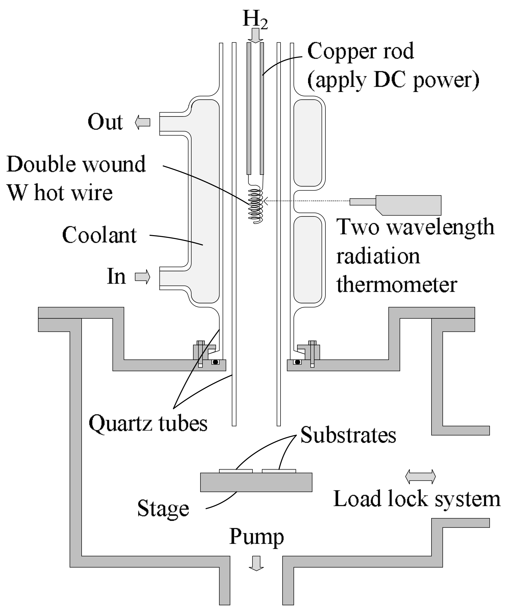
Figure 1 shows schematic of a remote-type hot-wire tool as atomic hydrogen generator. Introduced H2 gas is dissociated to atomic hydrogen on the electrical heated tungsten wire surface by catalytic reaction. The tungsten wire inside a quartz tube is double wound (wire diameter: 0.5 mm, length: 450 mm, inside/outside winding diameter: 4/9 mm) to prevent thermal deformation. Generated atomic hydrogen at the hot wire is carried to the substrates along with high-speed viscous H2 flow. Because the annihilation of atomic hydrogen in the carrier gas (H2) is suppressed by Reaction (1),
and the deactivation rate of atomic hydrogen on quartz surface is much lower than that on metals, a sample substrate can be treated with high atomic hydrogen density. The hot-wire temperature reaches 2100 °C measured by a two-wavelength radiation thermometer. However, the wafer substrate temperature during atomic hydrogen irradiation is lower than 100 °C, because thermal radiation from the hot wire is reduced by keeping a proper distance between the hot wire and the wafer. In this setup, the solid angle of the hot wire from the substrate is sufficiently small (~0.0023 sr), and the amount of the radiation to the substrates is negligibly small. Thus, the substrate stage temperature and hot-wire temperature can be controlled independently.
H2 + H• → H• + H2,
Atomic hydrogen density on the substrates evaluated by transmittance change of WO3 doped phosphate glass [27] is approximately 5.0 × 1012 cm−3, which is one order of magnitude higher than that in plasma [24]. H2 pressure in the chamber is controlled at 130 Pa by 500 sccm of H2 flow rate under evacuation by a mechanical booster pump.
2.2. Bonding Sample Preparation
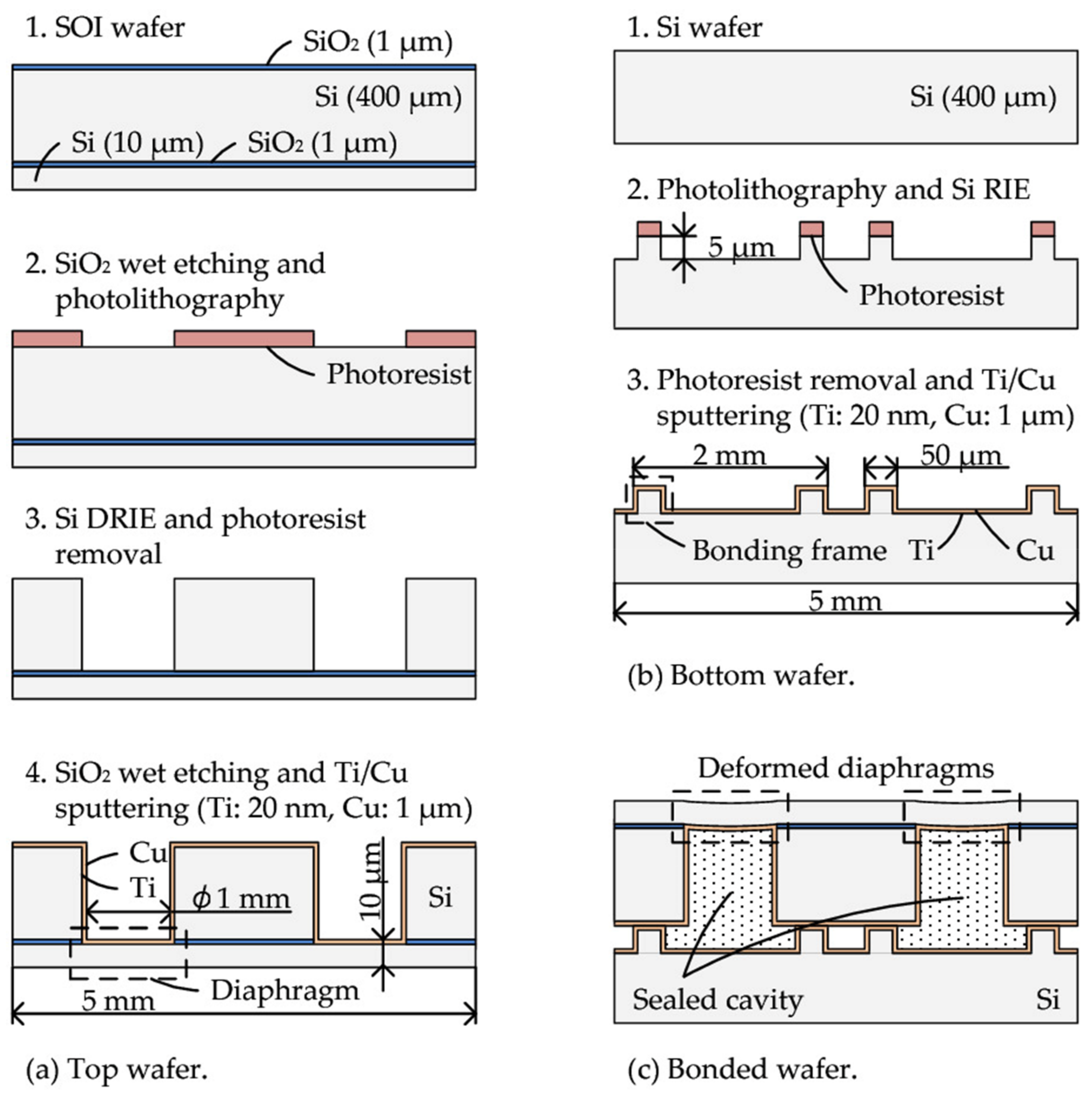
Cu-Cu bonding is carried out by using a pair of 2 cm square sample wafers, because physics and the principle of bonding procedure for a 2 cm square wafer is essentially the same as larger wafers, and the developed bonding technology can be scalable to larger wafers. The fabrication processes are shown in Figure 2. A top wafer (cavity wafer) has cavities, and 10 µm thick Si diaphragms made by DRIE (deep reactive ion etching) of a silicon-on-insulator (SOI) wafer with a 10 µm-thick device layer followed by wet HF etching of a 1 µm-thick buried oxide (BOX) layer (Figure 2a). Each completed 2 cm square wafer has 36 diaphragms with 1 mm diameter. A bottom wafer (bonding frame wafer) has 10 µm high and 50 µm wide bonding frame structures made by Si DRIE (Figure 2b). On both wafers, 20 nm of Ti as adhesion layer and 1 µm of Cu layers as bonding layer were deposited by RF magnetron sputtering. Figure 2c shows completed samples after wafer bonding.
2.3. Pre-Treatment and Wafer Bonding
Citric acid pre-treatment and atomic hydrogen pre-treatment conditions are shown in Table 1. The top wafer and the bottom wafer are pre-treated at the same time and intentionally exposed to the atmosphere at 25 °C for 1 h or 24 h under 50% of relative humidity. The pair of wafers are introduced into a lab-made bonding system [28]. After bonding chamber pressure has reached 1.0 × 10⁻² Pa by a turbo molecular pump, the wafers are aligned and transferred to the bonding stage at pre-set bonding temperature. Then the wafers are bonded by 70 MPa of bonding pressure. A graphite sheet is inserted between the bottom wafer and the bonding stage to uniformize bonding pressure distribution. The bonding conditions are shown in Table 2.
2.4. Evaluation of Bonding Performance
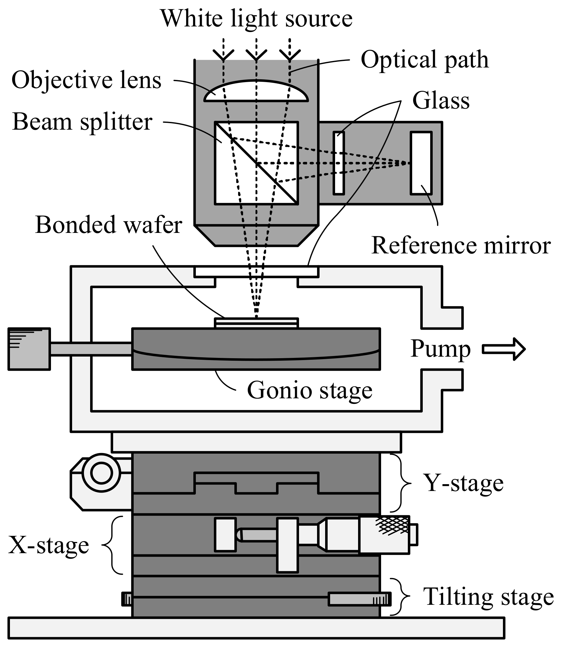
The accomplishment of vacuum sealing is judged by the deflection of the diaphragm due to differential pressure between the inside and outside of the cavity. Vacuum sealing yield is defined by dividing the number of deflected diaphragms by the total number of diaphragms. The actual pressure in the sealed cavity is evaluated by the 10 μm-thick diaphragm deformation in a pressure-controllable vacuum chamber at different pressures at 25 °C. The pressure inside the cavity is identical to the chamber pressure when the diaphragm is flat; this is called zero-balance method [9,29,30]. The deformation of the diaphragm is measured by a white light interferometry surface topography measurement system (MSA-500 Micro System Analyzer, Polytec GmbH, Waldbronn, Germany) through a glass window on the chamber, as shown in Figure 3. The leak rate of the hermetic sealed devices is evaluated by cavity pressure change with storage time in the air at 25 °C.
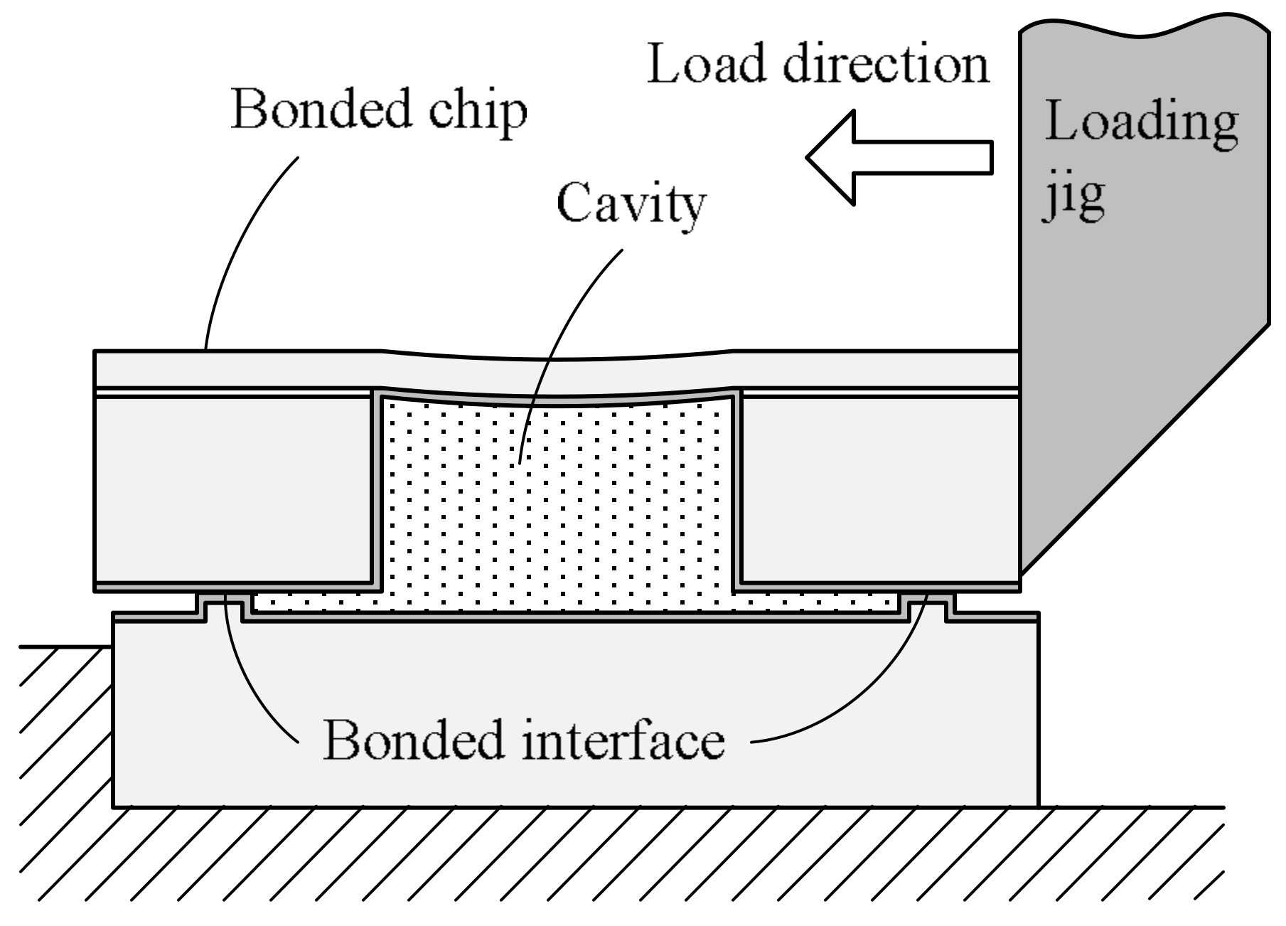
The bonding strength of the bonded wafers is evaluated using a shear tester (PTR-1101, Rhesca, Tokyo, Japan) at 25 °C. The schematic of the shear test setup is shown in Figure 4. The bonded wafers are diced into 2.5 mm square chips which have a single bonding frame. Shear force is applied to the bonded chip in the horizontal direction using the loading jig.
2.5. AES and TDS Measurements
Cu surface compositions change after the treatment by citric acid or atomic hydrogen is evaluated using X-ray induced AES measurement. A Mg-Kα X-ray source is used to separate the AES peaks of Cu2O and Cu.
Desorbed gas species from the treated Cu surface were identified by TDS method (TDS1200, ESCO, Ltd., Tokyo, Japan) at temperatures ranging from 50 to 500 °C, which simulates the bonding procedure. The heating rate is 1 K/s. [31,32]. The analysis of the TDS measurement system is quantitatively calibrated by hydrogen-implanted silicon samples.
The sample preparation and pre-treatment condition for the AES and TDS measurements are the same as the bonding experiment as shown in Table 1.
3. Results
3.1. Yield of Hermetic Sealing
Figure 5a,b show the hermetic sealing yield of citric acid pre-treated wafer and the atomic hydrogen pre-treated wafer, respectively. Both wafers are intentionally exposed in the air for 1 h before bonding. The citric acid pre-treated wafers require bonding temperature higher than 350 °C for hermetic sealing. In contrast, hermetic Cu-Cu bonding was successfully demonstrated as low as 300 °C after atomic hydrogen pre-treatment. Even after exposing the wafers for 24 h in air after pre-treatment by atomic hydrogen, hermetic sealing was achieved. Therefore, atomic hydrogen treatment can improve hermetic sealing tolerance against air exposure and greatly relax the time constraint between the pretreatment and bonding process.
3.2. Bonding Strength
Figure 6 shows the shear strengths of the bonded chips in different conditions. The shear strengths of the citric acid pre-treated wafer bonded at 300 °C is not evaluated because of zero hermetic sealing yield. The shear strength of the citric acid pre-treated chips and the atomic hydrogen pre-treated chips are 130 MPa and a range between 80 and 100 MPa, respectively. The shear strength of the atomic hydrogen pre-treated chips is lower than that of the citric acid pre-treated chips. However, it can be applied for actual use because the strength is sufficiently higher than MIL-STD-883G requirement (12.6 MPa) for the packaged devices [33].
3.3. Pressure of Sealed Cavity
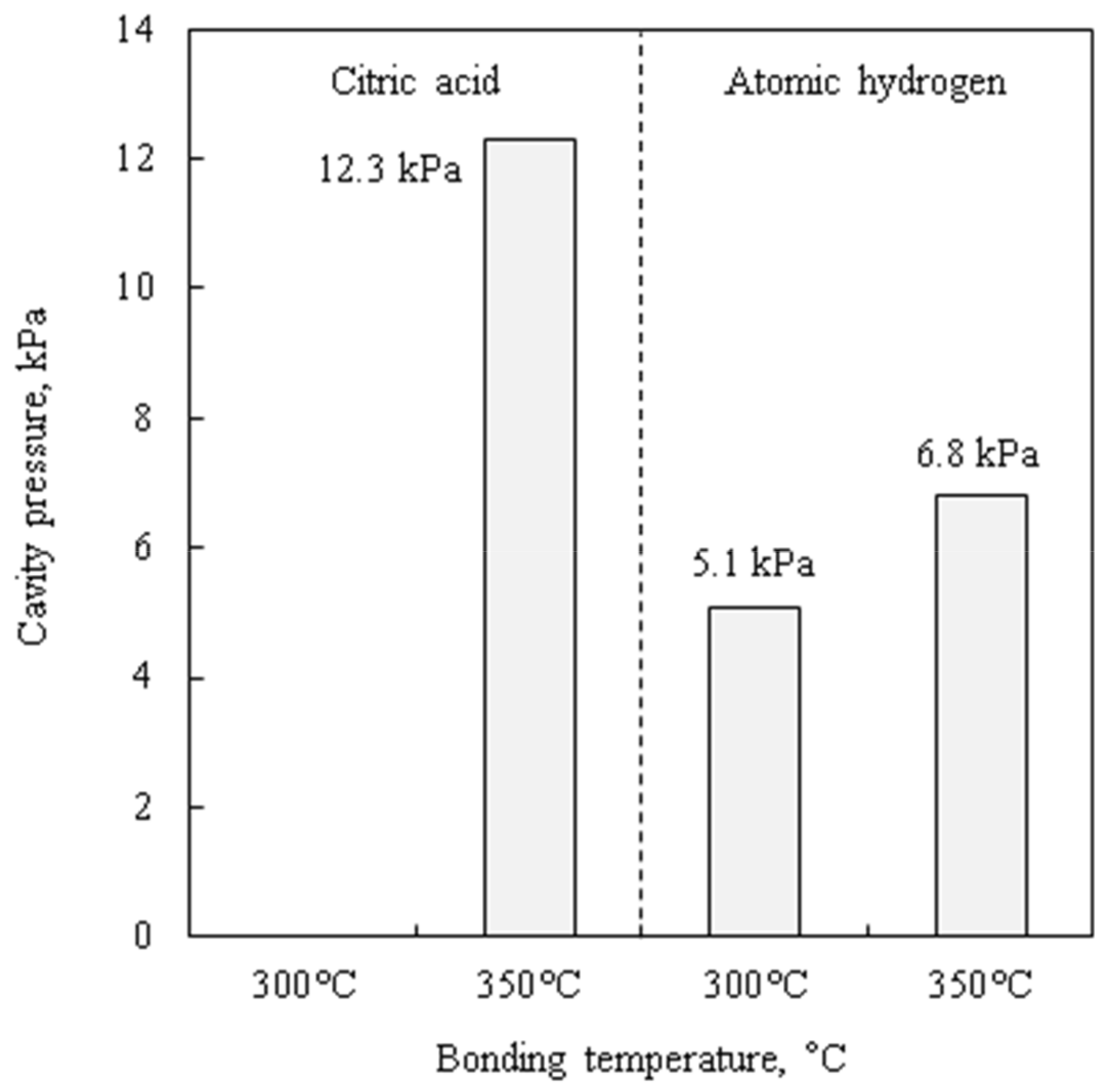
Figure 7 shows sealed cavity pressures measured by the zero-balance method. The cavity pressure of the citric acid pre-treated wafer bonded at 300 °C cannot be evaluated because no sealed cavity is obtained. The cavity pressure is larger than 5 kPa, even though the bonding is performed under 1.0 × 10⁻² Pa. The remaining cavity pressure is considered to be thermally desorbed gas from adsorbed molecules on the Cu films by the result of TDS measurements. The atomic hydrogen-treated wafers have approximately half the pressure of the citric acid-treated one. It is considered that atomic hydrogen reacts and decomposes adsorbed species on the Cu films. Bonding temperature lower than gas desorption temperature can reduce cavity pressure. The usage of getter materials for residual gas adsorption can also improve vacuum level.
3.4. Leak Rate
Figure 8 shows change of the cavities pressure with storage time. The cavity pressure is decreased in the initial 20 days on both citric acid pre-treated sample and atomic hydrogen pre-treated sample. It is considered that the residual gas molecules are re-adsorbed on the Cu surfaces. The coverage of the re-adsorbed molecules on the cavity inside wall of the citric acid and atomic hydrogen pre-treated samples are a 0.9 and 1.7 mono layer, respectively, which are in a reasonable range of typical gas adsorption on a Cu surface.
Estimated leak rate in the worst case by considering the detection error of the zero-balance method (several hundred Pa) is lower than 10−14 Pa m3 s−1 order, which is sufficiently low compared to the reported value by Au-Au bonding [9], and is at least six orders of magnitude lower than that in the rejection limit for military and aerospace electronic systems use defined by the MIL-STD-883G specification of 5.0 × 10⁻⁹ (Pa·m3)/s [34].
3.5. AES Measurements: Observation of Cu Re-Oxidation in Atmosphere
AES spectra of the treated Cu surfaces are shown in Figure 9. The AES peaks at 336.8 eV and 334.9 eV are identified as the binding energy of Cu2O and metal Cu, respectively [35,36]. Figure 9a shows that the Cu2O peak is already dominant after 1 h exposure to air after the citric acid treatment. In contrast, the metal Cu peak is still dominant after 24 h from the atomic hydrogen treatment, as shown in Figure 9b. These results indicate that the role of atomic hydrogen treatment is not only surface oxide removal but also the prevention of oxide growth on Cu surface in the air.
3.6. TDS Measurements: Observation of Chemisorbed Hydrogen Atoms on Cu Surface
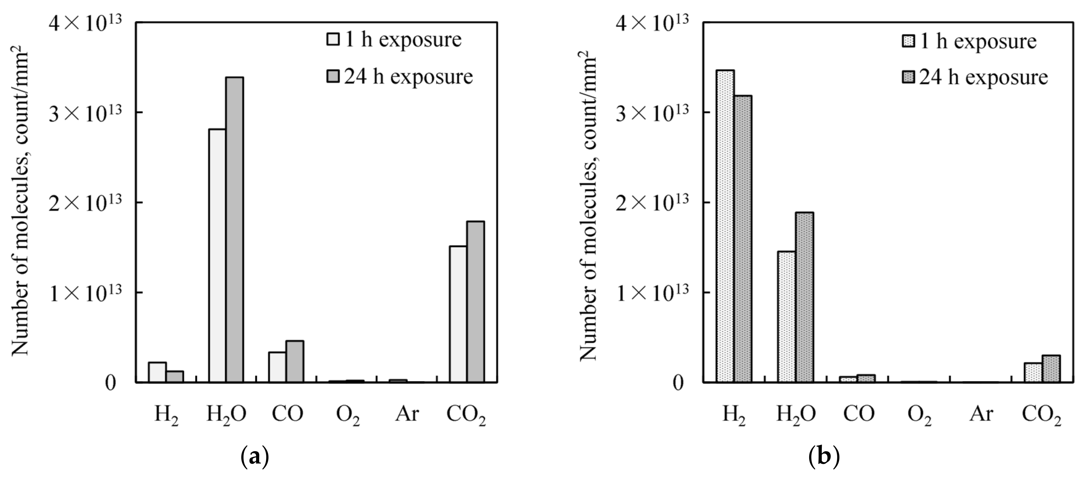
The spectrum of thermally desorbed molecules from the pretreated Cu films are shown in Figure 10. Most of the desorbed gas species from the citric acid-treated Cu films are H2O, CO, and CO2, as shown in Figure 10a. These gas species are typical adsorption molecules on Cu surface. On the other hand, for the atomic hydrogen-treated Cu films, the amount of typical desorbed gas is smaller than that from that of the citric acid-treated one. However, a large amount of H2 gas is desorbed as shown in Figure 10b. The desorbed H2 gas may be generated from the chemisorbed hydrogen which is directly formed from the atomic hydrogen irradiation [37].
Figure 11 shows the amount of the desorbed molecules by integrating TDS peaks. The atomic hydrogen-treated Cu film is occupied with chemisorbed hydrogen even after 24 h storage in the air, as shown in Figure 11a, while chemisorbed hydrogen is not dominant on the citric acid-treated Cu film, as shown in Figure 11b. These results indicate that the chemisorbed hydrogen on the atomic hydrogen-treated Cu surface is stable even in the air, and suppresses other chemical species adsorption, not only oxide, but also carbon species.
3.7. Reasons for Low-temperature Vacuum Seal Capability after Storage in Atmospheric Condition
The AES and TDS results indicate that the atomic hydrogen pre-treatment removes Cu native oxide and then forms hydride-like layers such as surface hydrogen or hydroxyl group, which suppress re-oxidation on the Cu surfaces during the wafer storage in atmospheric condition. The hydride-like layer growth on the Cu surface by hydrogen plasma treatment has been reported [21,22,38], and such surface hydrogen species can also suppress the re-oxidation of the Cu surfaces [38]. Such re-oxidation suppression by the chemisorbed hydrogen may enable vacuum sealing at far lower temperature by the atomic hydrogen pre-treatment in comparison with the conventional wet oxide reduction. Moreover, low pre-treatment temperature below Cu re-crystallization point does not promote the coalescence of Cu fine grains, which should proceed during the bonding process instead of the pre-treatment process. Interfacial gap/void filling by the Cu coalescence also plays a key role during low-temperature wafer bonding [16].
It should be noted that the Cu hydride-like layer does not need to be removed by an additional process before bonding, while the surface protection layer such as Cu3N or SAM must be removed by thermal treatment before bonding [22,39]. It is considered that desorbed hydrogen atoms can diffuse into the Cu crystals due to their small atomic radius. However, there is a possibility that the strength of the atomic hydrogen-treated wafer is deteriorated due to hydrogen embrittlement. In fact, the shear strengths of the atomic hydrogen-treated wafers were 26–36% lower than the citric acid-treated ones, as shown in Figure 6.
4. Conclusions
Wafer-level vacuum sealing by Cu-Cu thermo-compression bonding was achieved at 300 °C by atomic hydrogen pre-treatment for Cu native oxide reduction using a remote-type hot-wire method, while 350 °C of Cu-Cu bonding temperature for vacuum sealing was needed by conventional Cu native oxide reduction using citric acid treatment. The remote-type tool prevents substrate heating by radiation from a hot wire during atomic hydrogen irradiation. As a result, substrate temperature is suppressed below 100 °C, which is lower than re-crystallization temperature of Cu nano-crystal. The removal of Cu native oxide and the suppression of re-oxidation during the storage of a substrate in the air due to chemisorbed hydrogen species on the Cu surfaces are explained by AES and TDS measurements. Vacuum sealing yield, pressure in the sealed cavity, leak rate and bonding strength by Cu-Cu bonding using the atomic hydrogen pre-treatment are almost equivalent to conventional Cu-Cu bonding at higher temperatures using wet oxide removal procedures. This technology will contribute to further low-temperature and low-damage Cu-Cu bonding for hermetic packaging.
Acknowledgments
This study was performed in R&D Center of Excellence for Integrated Microsystems, Tohoku University, supported by the Formation of Innovation Center for Fusion of Advanced Technologies, and partially supported by the New Energy and Industrial Technology Development Organization (NEDO).
Author Contributions
Koki Tanaka, Hideki Hirano, Masafumi Kumano, Joerg Froemel and Shuji Tanaka conceived and designed the experiments; Koki Tanaka and Masafumi Kumano set up experimental tools. Koki Tanaka performed the experiments and analyzed the data; Koki Tanaka and Hideki Hirano prepared the manuscript.
Conflicts of Interest
The authors declare no conflict of interest.
References
- Santagata, F.; Creemer, J.F.; Iervolino, E.; Sarro, P.M. Tube-shaped Pirani gauge for in situ hermeticity monitoring of SiN thin-film encapsulation. J. Micromech. Microeng. 2012, 22, 105025. [Google Scholar] [CrossRef]
- Esashi, M. Wafer level packaging of MEMS. J. Micromech. Microeng. 2008, 18, 73001. [Google Scholar] [CrossRef]
- Fischer, A.C.; Forsberg, F.; Lapisa, M.; Bleiker, S.J.; Stemme, G.; Roxhed, N.; Niklaus, F. Integrating MEMS and ICs. Microsyst. Nanoeng. 2015, 1, 15005. [Google Scholar] [CrossRef]
- Harendt, C.; Graf, H.G.; Hofflinger, B.; Penteker, E. Silicon fusion bonding and its characterization. J. Micromech. Microeng. 1992, 2, 113–116. [Google Scholar] [CrossRef]
- Henmi, H.; Shoji, S.; Shoji, Y.; Yoshimi, K.; Esashi, M. Vacuum packaging for microsensors by glass-silicon anodic bonding. Sens. Actuators A Phys. 1994, 43, 243–248. [Google Scholar] [CrossRef]
- Tanaka, S. Wafer-level hermetic MEMS packaging by anodic bonding and its reliability issue. Microelectron. Reliab. 2014, 54, 875–881. [Google Scholar] [CrossRef]
- Knechtel, R. Glass frit bonding: An universal technology for wafer level encapsulation and packaging. Microsyst. Technol. 2005, 12, 63–68. [Google Scholar] [CrossRef]
- Aasmundtveit, K.E.; Luu, T.T.; Tollefsen, T.A.; Wang, K.; Nguyen, H.V.; Hoivik, N. Solid-Liquid Interdiffusion (SLID) Bonding. In Proceedings of the 2016 Symposium on Design, Test, Integration & Packaging of MEMS and MOEMS, Budapest, Hungary, 30 May–2 June 2016. [Google Scholar]
- Al Farisi, M.S.; Hirano, H.; Frömel, J.; Tanaka, S. Wafer-level hermetic thermo-compression bonding using electroplated gold sealing frame planarized by fly-cutting. J. Micromech. Microeng. 2017, 27, 15029. [Google Scholar] [CrossRef]
- Chen, K.N.; Tan, C.S.; Fan, A.; Reif, R. Morphology and Bond Strength of Copper Wafer Bonding. Electrochem. Solid-State Lett. 2004, 7, G14. [Google Scholar] [CrossRef]
- Baum, M.; Hofmann, L.; Wiemer, M.; Schulz, S.; Gessner, T. Development and characterisation of 3D integration technologies for MEMS based on copper filled TSV’s and copper-to-copper metal thermo compression bonding. In Proceedings of the IEEE 2013 International Semiconductor Conference Dresden—Grenoble (ISCDG), Dresden, Germany, 26–27 September 2013; pp. 1–4. [Google Scholar]
- Kim, T.H.; Howlader, M.M.R.; Itoh, T.; Suga, T. Room temperature Cu–Cu direct bonding using surface activated bonding method. J. Vac. Sci. Technol. A 2003, 21, 449–453. [Google Scholar] [CrossRef]
- Wu, Z.; Cai, J.; Wang, Q.; Wang, J. Low temperature Cu–Cu bonding using copper nanoparticles fabricated by high pressure PVD. AIP Adv. 2017, 7, 035306. [Google Scholar] [CrossRef]
- Derby, B.; Wallach, E.R. Diffusion bonds in copper. J. Mater. Sci. 1984, 19, 3140–3148. [Google Scholar] [CrossRef]
- Takahashi, Y.; Takahashi, K.; Nishiguchi, K. A numerical analysis of void shrinkage processes controlled by coupled surface and interface diffusion. Acta Metall. Mater. 1991, 39, 3199–3216. [Google Scholar] [CrossRef]
- Sakai, T.; Imaizumi, N.; Sakuyama, S. A Low Temperature Cu-Cu Direct Bonding Method with VUV and HCOOH Treatment for 3D Integration. In Proceedings of the 2015 International Conference on Electronic Packaging and iMAPS All Asia Conference, Kyoto, Japan, 14–17 April 2015; pp. 464–467. [Google Scholar]
- Tateishi, H.; Susaki, A.; Nakada, T. Development of the System for Cu Oxide Film Removal from Semiconductor Interconnects in Atmosphere pressure. Ebara Eng. Rev. 2008, 218, 40–44. [Google Scholar]
- Lim, D.F.; Fan, J.; Peng, L.; Leong, K.C.; Tan, C.S. Cu–Cu Hermetic Seal Enhancement Using Self-Assembled Monolayer Passivation. J. Electron. Mater. 2013, 42, 502–506. [Google Scholar] [CrossRef]
- Tan, C.S.; Lim, D.F.; Singh, S.G.; Goulet, S.K.; Bergkvist, M. Cu–Cu diffusion bonding enhancement at low temperature by surface passivation using self-assembled monolayer of alkane-thiol. Appl. Phys. Lett. 2009, 95, 192108. [Google Scholar] [CrossRef]
- Chang, Y.; Leu, J.; Lin, B.; Wang, Y.; Cheng, Y. Comparison of H2 and NH3 Treatments for Copper Interconnects. Adv. Mater. Sci. Eng. 2013, 1–7. [Google Scholar] [CrossRef]
- Baklanov, M.R.; Shamiryan, D.G.; Tökei, Z.; Beyer, G.P.; Conard, T.; Vanhaelemeersch, S.; Maex, K. Characterization of Cu surface cleaning by hydrogen plasma. J. Vac. Sci. Technol. B 2001, 19, 1201. [Google Scholar] [CrossRef]
- Tanaka, K.; Wang, W.-S.; Baum, M.; Froemel, J.; Hirano, H.; Tanaka, S.; Wiemer, M.; Otto, T. Investigation of Surface Pre-Treatment Methods for Wafer-Level Cu–Cu Thermo-Compression Bonding. Micromachines 2016, 7, 234. [Google Scholar] [CrossRef]
- Izumi, A.; Ueno, T.; Miyazaki, Y.; Oizumi, H.; Nishiyama, I. Reduction of oxide layer on various metal surfaces by atomic hydrogen treatment. Thin Solid Films 2008, 516, 853–855. [Google Scholar] [CrossRef]
- Umemoto, H.; Ohara, K.; Morita, D.; Nozaki, Y.; Masuda, A.; Matsumura, H. Direct detection of H atoms in the catalytic chemical vapor deposition of the Si4/H2 system. J. Appl. Phys. 2002, 91, 1650–1656. [Google Scholar] [CrossRef]
- Karasawa, M.; Masuda, A.; Ishibashi, K.; Matsumura, H. Development of Cat-CVD apparatus—A method to control wafer temperatures under thermal influence of heated catalyzer. Thin Solid Films 2001, 395, 71–74. [Google Scholar] [CrossRef]
- Tanaka, K.; Kumano, M.; Tanaka, S. Removal of SU-8 by two types of hot-wire atomic hydrogen sources—Dissection of contributions by atomic hydrogen and substrate heating. J. Vac. Sci. Technol. B 2015, 33, 52001. [Google Scholar] [CrossRef]
- Morimoto, T.; Umemoto, H.; Yoneyama, K.; Masuda, A.; Matsumura, H.; Ishibashi, K.; Tawarayama, H.; Kawazoe, H. Quantification of Gas-Phase H-Atom Number Density by Tungsten Phosphate Glass. Jpn. J. Appl. Phys. 2005, 44, 732–735. [Google Scholar] [CrossRef]
- Matsuzaki, S.; Tanaka, S.; Esashi, M. Anodic bonding between LTCC wafer and Si wafer with Sn-Cu-based electrical connection. Electron. Commun. Jpn. 2012, 95, 49–56. [Google Scholar] [CrossRef]
- Timoshenko, S.; Woinowsky-krieger, S. Theory of Plates and Shells, 2nd ed.; McGraw-Hill Publishing Company: New York, NY, USA, 1989; ISBN 0070647798. [Google Scholar]
- Eaton, W.P.; Bitsie, F.; Smith, J.H.; Plummer, D.W. A New Analytical Solution for Diaphragm Deflection and Its Application to a Surface-Micromachined Pressure Sensor. In Technical Proceedings of the 1999 International Conference on Modeling and Simulation of Microsystems; Nano Science and Technology Institute: Danville, CA, USA, 1999; pp. 640–643. [Google Scholar]
- Hirashita, N.; Uchiyama, T. Quantitative desorption analysis of ultra large scale integration materials by thermal desorption spectroscopy. Bunseki Kagaku 1994, 43, 757–764. [Google Scholar] [CrossRef]
- Hirashita, N.; Urano, M.; Yoshida, H. Measurements of Outgassing Rates in a Field of Analysis. J. Vac. Soc. Jpn. 2014, 57, 214–218. [Google Scholar] [CrossRef]
- United States Department of Defense. Method 2019.7 Die Shear Strength. MIL-STD-883G. In Test Method Standard Microcircuits; Defense Supply Center Columbus ATTN: Columbus, OH, USA, 2003; pp. 1–5. [Google Scholar]
- United States Department of Defense. Method 1014.12. MIL-STD-883G. In Test Method Standard Microcircuits; Defense Supply Center Columbus ATTN: Columbus, OH, USA, 2006; pp. 1–6. [Google Scholar]
- McIntyre, N.S.; Sunder, S.; Shoesmith, D.W.; Stanchell, F.W. Chemical information from XPS—Applications to the analysis of electrode surfaces. J. Vac. Sci. Technol. 1981, 18, 714–721. [Google Scholar] [CrossRef]
- Sawada, Y.; Tamaru, H.; Kogoma, M.; Kawase, M.; Hashimoto, K. The reduction of copper oxide thin films with hydrogen plasma generated by an atmospheric-pressure glow discharge. J. Phys. D Appl. Phys. 1999, 29, 2539–2544. [Google Scholar] [CrossRef]
- Christmann, K. Interaction of hydrogen with solid surfaces. Surf. Sci. Rep. 1988, 9, 1–163. [Google Scholar] [CrossRef]
- Shin, S.; Higurashi, E.; Furuyama, K.; Suga, T. Hydrogen Radical Treatment for Suppression of Oxidation and Contamination at Copper Surfaces. In Proceedings of the 34th Sensor Symposium on Sensors Micromachines and Applied Systems, Hiroshima, Japan, 31 October–2 November 2017. [Google Scholar]
- Lim, D.F.; Singh, S.G.; Ang, X.F.; Wei, J.; Ng, C.M.; Tan, C.S. Achieving low temperature Cu to Cu diffusion bonding with self assembly monolayer (SAM) passivation. In Proceedings of the 2009 IEEE International Conference on 3D System Integration, San Francisco, CA, USA, 28–30 September 2009; IEEE: New York, NY, USA, 2009; pp. 1–5. [Google Scholar]
Figure 1.
Schematic of the remote-type hot-wire tool.

Figure 2.
Fabrication processes of (a) the top wafer (cavity wafer), (b) the bottom wafer (bonding frame wafer) and (c) bonded wafer. Both wafer size is 2 cm square. Each wafer has 16 cavities with diaphragms and bonding frames.
Figure 2.
Fabrication processes of (a) the top wafer (cavity wafer), (b) the bottom wafer (bonding frame wafer) and (c) bonded wafer. Both wafer size is 2 cm square. Each wafer has 16 cavities with diaphragms and bonding frames.

Figure 3.
Schematic of the sealed cavity pressure evaluation by zero-balance method.

Figure 4.
Schematic of bonding shear strength evaluation.

Figure 5.
Yields of the hermetic sealed cavities. A pair of bonding wafers is exposed to the atmosphere for 1 h after each pre-treatment. (a) Citric acid treated wafer. (b) Atomic hydrogen treated wafer.
Figure 5.
Yields of the hermetic sealed cavities. A pair of bonding wafers is exposed to the atmosphere for 1 h after each pre-treatment. (a) Citric acid treated wafer. (b) Atomic hydrogen treated wafer.
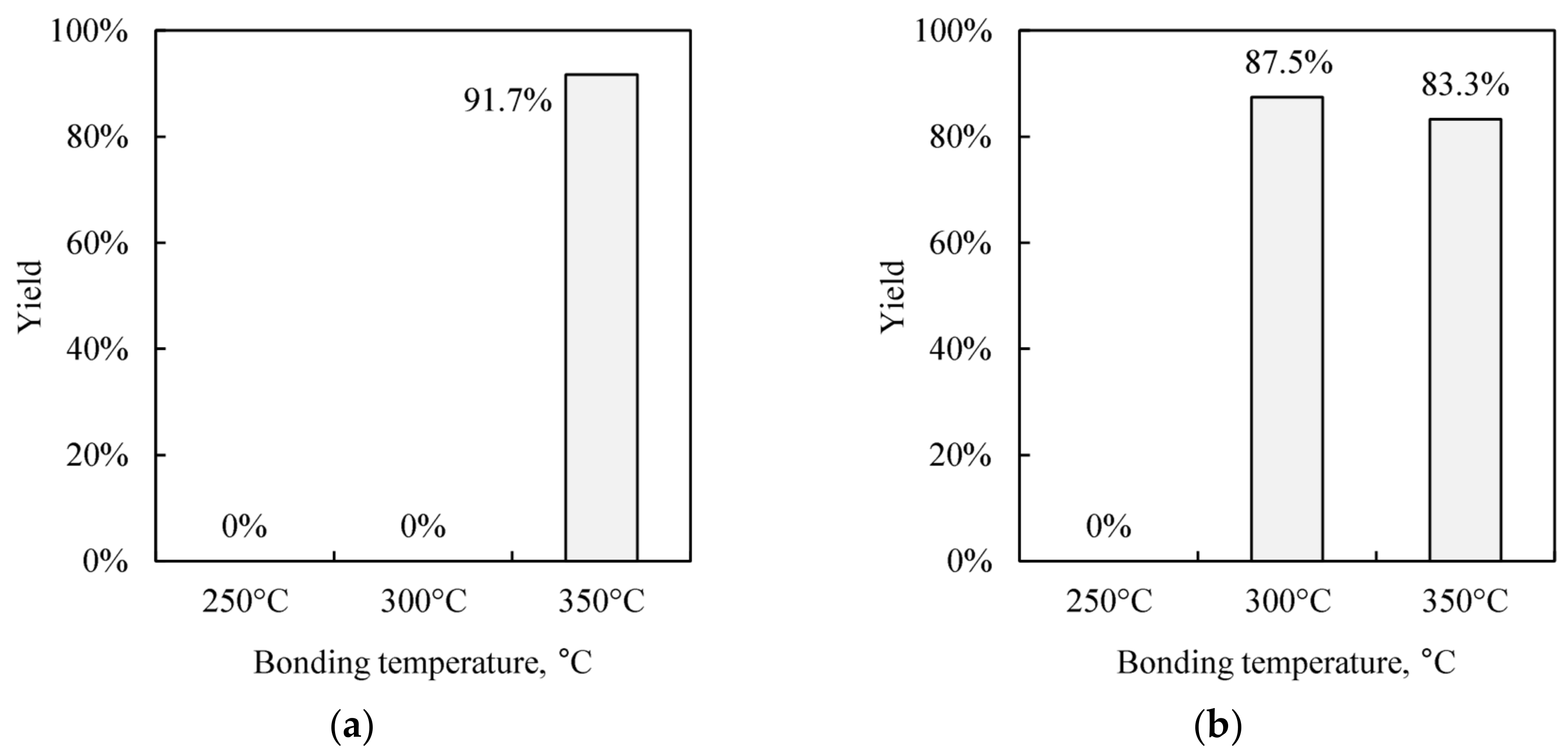
Figure 6.
Shear strengths of the bonded chips.
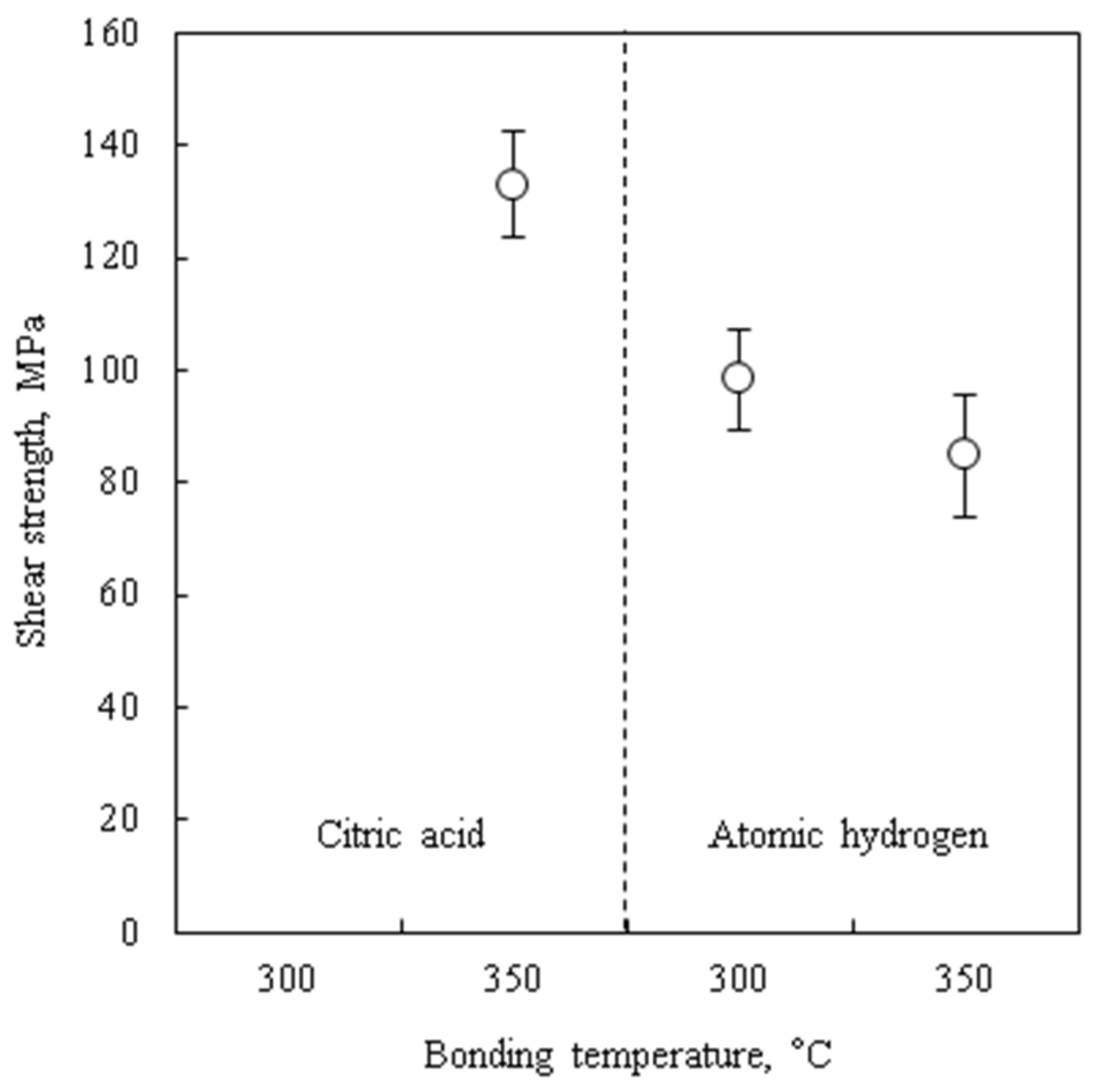
Figure 7.
Hermetic sealed cavities pressure measured by zero-balance method.

Figure 8.
Cavity pressure change with air exposure time. (a) Citric acid treated wafer, which was bonded at 350 °C. (b) Atomic hydrogen treated wafer, which was bonded at 300 °C.
Figure 8.
Cavity pressure change with air exposure time. (a) Citric acid treated wafer, which was bonded at 350 °C. (b) Atomic hydrogen treated wafer, which was bonded at 300 °C.
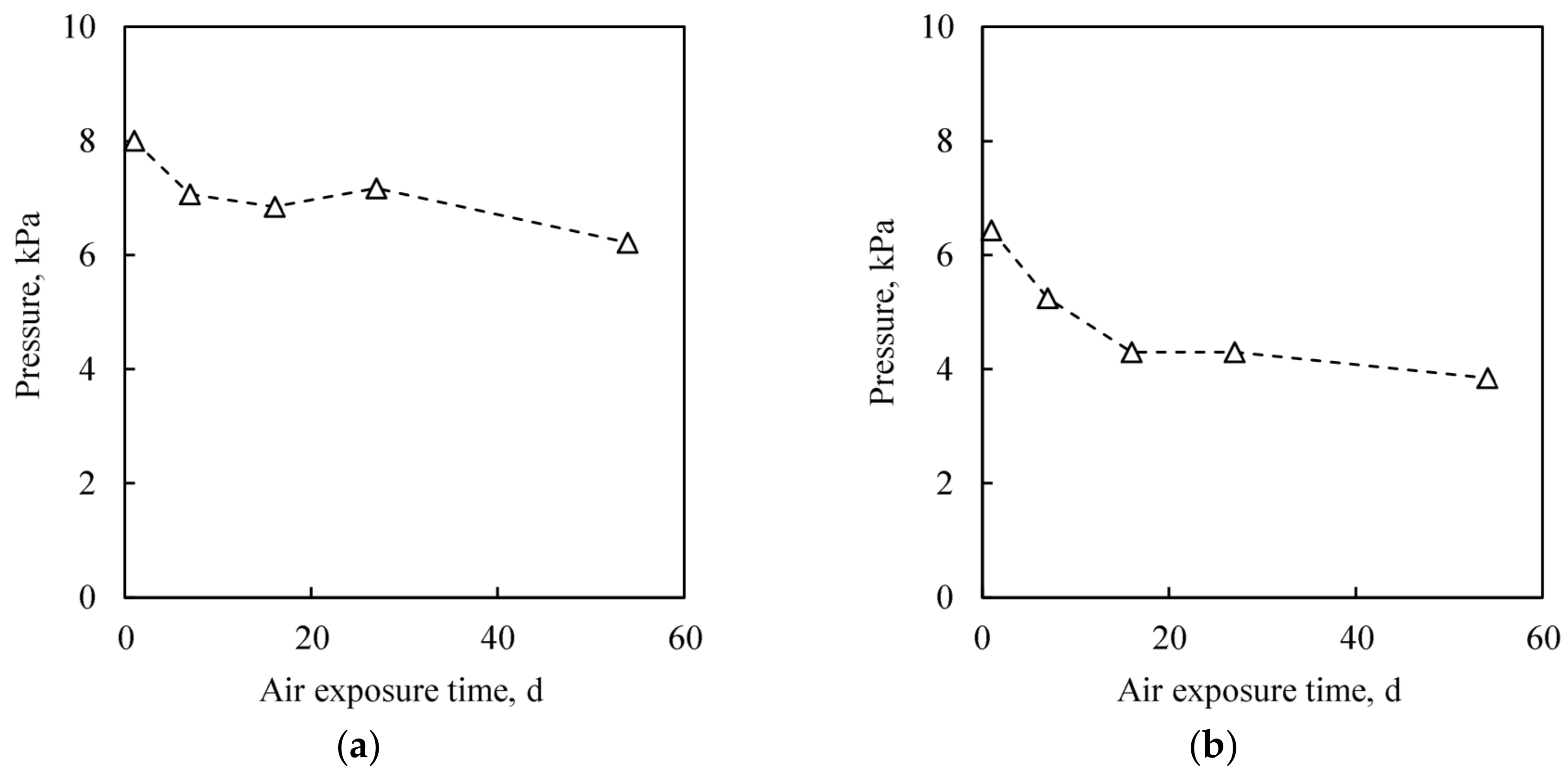
Figure 9.
AES spectra of the treated Cu films after exposed to the air for 1 or 24 h. (a) Citric acid treated Cu film. (b) Atomic hydrogen treated Cu film.
Figure 9.
AES spectra of the treated Cu films after exposed to the air for 1 or 24 h. (a) Citric acid treated Cu film. (b) Atomic hydrogen treated Cu film.
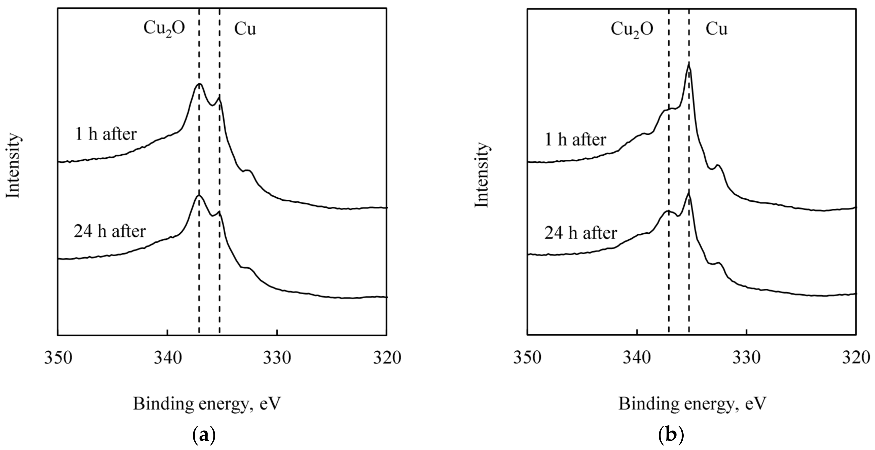
Figure 10.
TDS spectra of the treated Cu films after exposed to the atmosphere for 1 h. (a) Citric acid treated Cu film. (b) Atomic hydrogen treated Cu film.
Figure 10.
TDS spectra of the treated Cu films after exposed to the atmosphere for 1 h. (a) Citric acid treated Cu film. (b) Atomic hydrogen treated Cu film.

Figure 11.
Total amounts of desorbed molecules in the TDS measurements. The treated Cu films are exposed to the atmosphere for 1 or 24 h. (a) Citric acid treated Cu film. (b) Atomic hydrogen treated Cu film.
Figure 11.
Total amounts of desorbed molecules in the TDS measurements. The treated Cu films are exposed to the atmosphere for 1 or 24 h. (a) Citric acid treated Cu film. (b) Atomic hydrogen treated Cu film.


Table 1.
Pre-treatment conditions.
| Pre-Treatment | Treatment Temperature | Treatment Time | Remarks |
|---|---|---|---|
| Citric acid solution | 25 °C | 3 min | After 1 wt % citric acid solution in water, the wafers were rinsed by DI water and ethanol. |
| Atomic Hydrogen Irradiation | 100 °C | 10 min | H2 flow rate and gas pressure were 500 sccm and 130 Pa, respectively. The hot-wire was heated at 2000 °C. |
Table 2.
Cu-Cu bonding conditions.
| Bonding Temperature | Bonding Duration | Bonding Pressure | Ambient Pressure |
|---|---|---|---|
| 250, 300, 350 °C | 40 min | 70 MPa | 1.0 × 10⁻² Pa |
© 2018 by the authors. Licensee MDPI, Basel, Switzerland. This article is an open access article distributed under the terms and conditions of the Creative Commons Attribution (CC BY) license (http://creativecommons.org/licenses/by/4.0/).
Share and Cite
MDPI and ACS Style
Tanaka, K.; Hirano, H.; Kumano, M.; Froemel, J.; Tanaka, S. Bonding-Based Wafer-Level Vacuum Packaging Using Atomic Hydrogen Pre-Treated Cu Bonding Frames. Micromachines 2018, 9, 181. https://doi.org/10.3390/mi9040181
AMA Style
Tanaka K, Hirano H, Kumano M, Froemel J, Tanaka S. Bonding-Based Wafer-Level Vacuum Packaging Using Atomic Hydrogen Pre-Treated Cu Bonding Frames. Micromachines. 2018; 9(4):181. https://doi.org/10.3390/mi9040181
Chicago/Turabian StyleTanaka, Koki, Hideki Hirano, Masafumi Kumano, Joerg Froemel, and Shuji Tanaka. 2018. "Bonding-Based Wafer-Level Vacuum Packaging Using Atomic Hydrogen Pre-Treated Cu Bonding Frames" Micromachines 9, no. 4: 181. https://doi.org/10.3390/mi9040181
Note that from the first issue of 2016, this journal uses article numbers instead of page numbers. See further details here.