Three-Dimensional Finite Element Method Simulation of Perforated Graphene Nano-Electro-Mechanical (NEM) Switches

 , ,
, ,
Abstract
:1. Introduction
2. Methodology
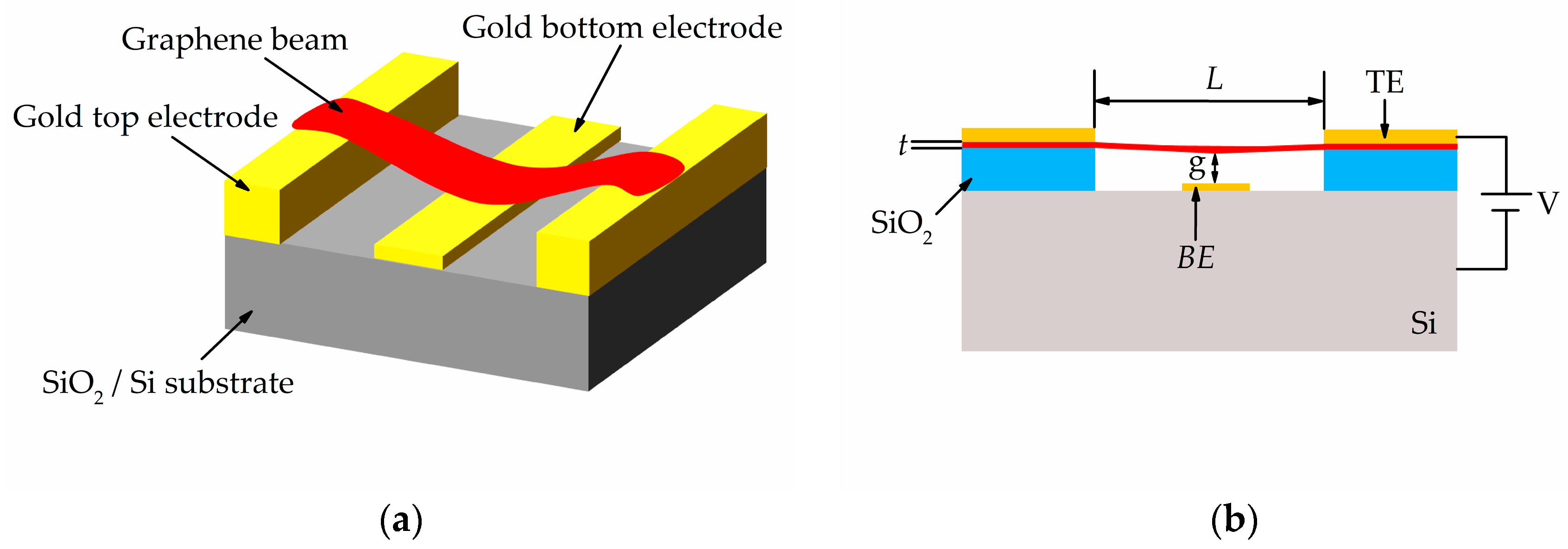
2.1. Description of Device Geometry and Operation Principles
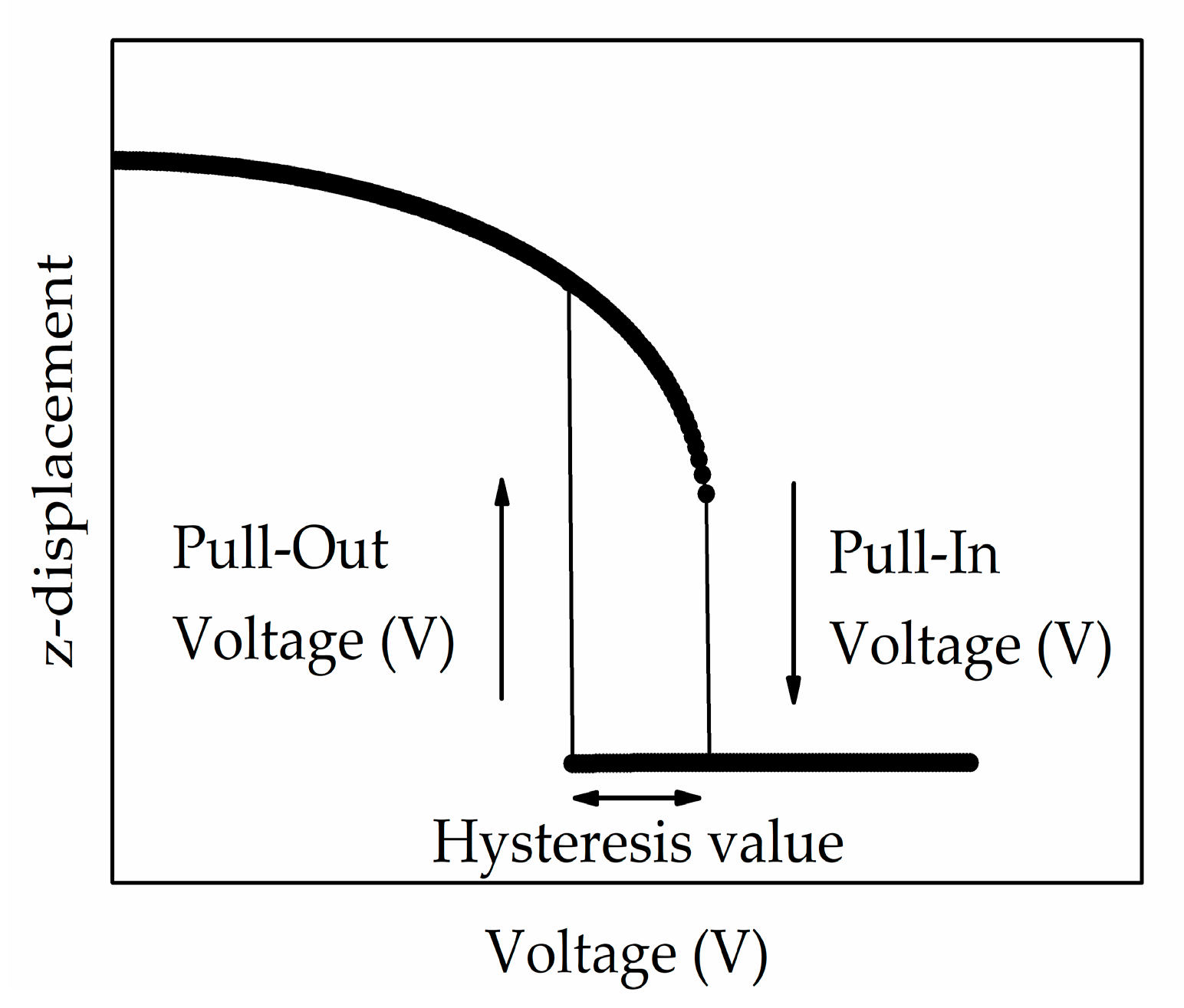
2.2. Thermo-Electromechanical (TEM) Analysis Model (FEM-IntelliSuite)
2.3. Empirical Equation of Actuation Pull-In Voltage
3. FEM Simulation Results and Discussion
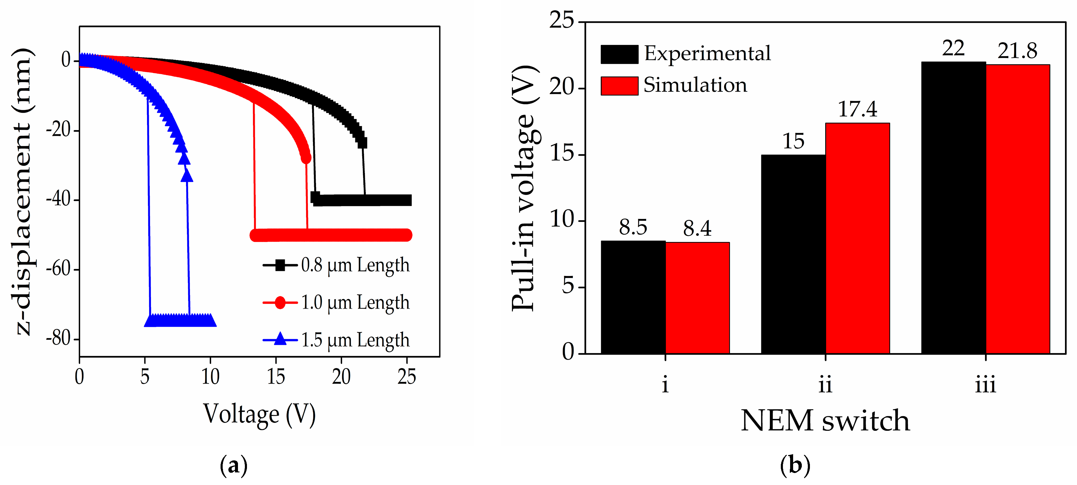
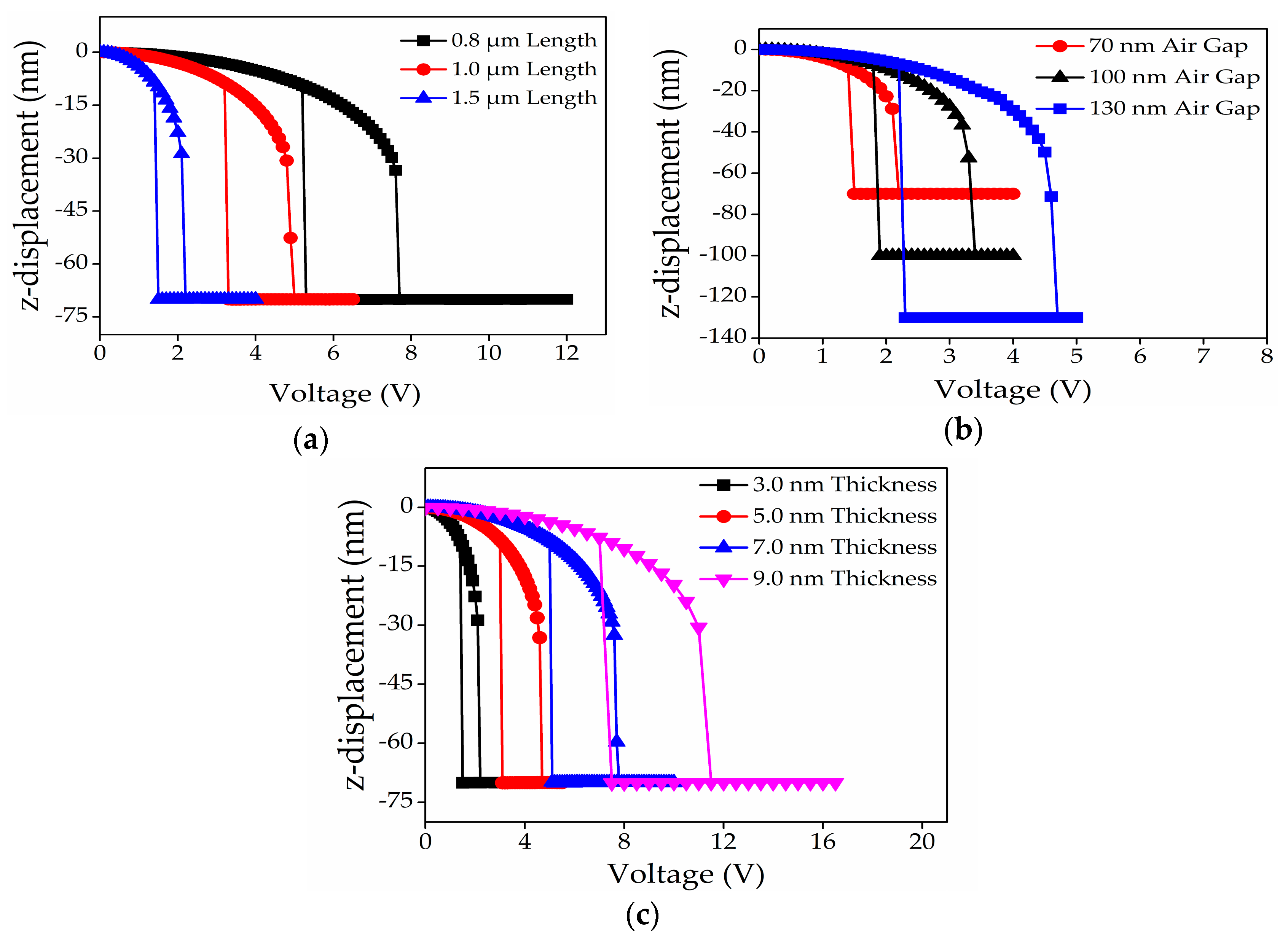
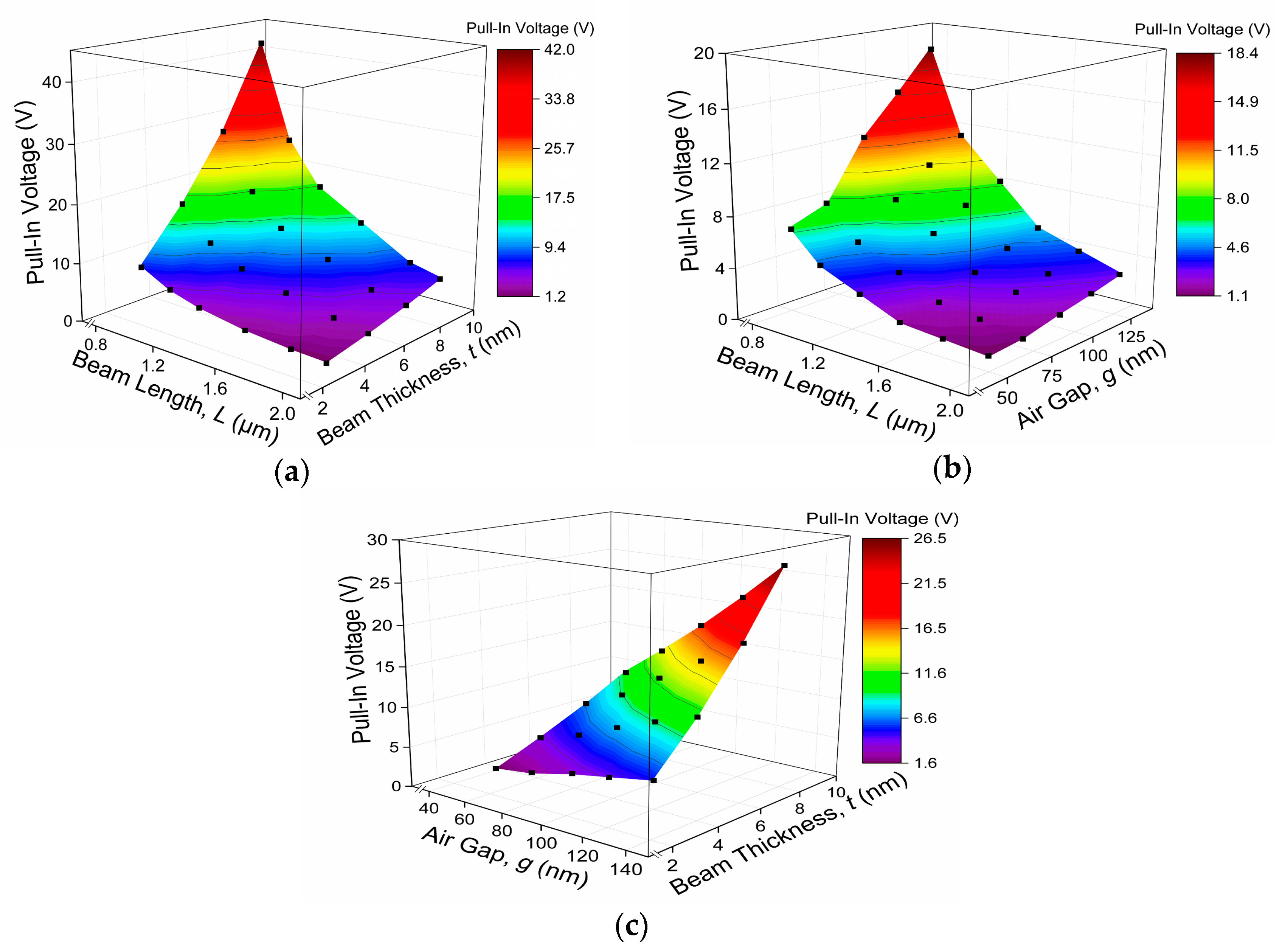
3.1. Analysis of Actuation Pull-In Voltage of Intact Graphene-Based NEM Switch
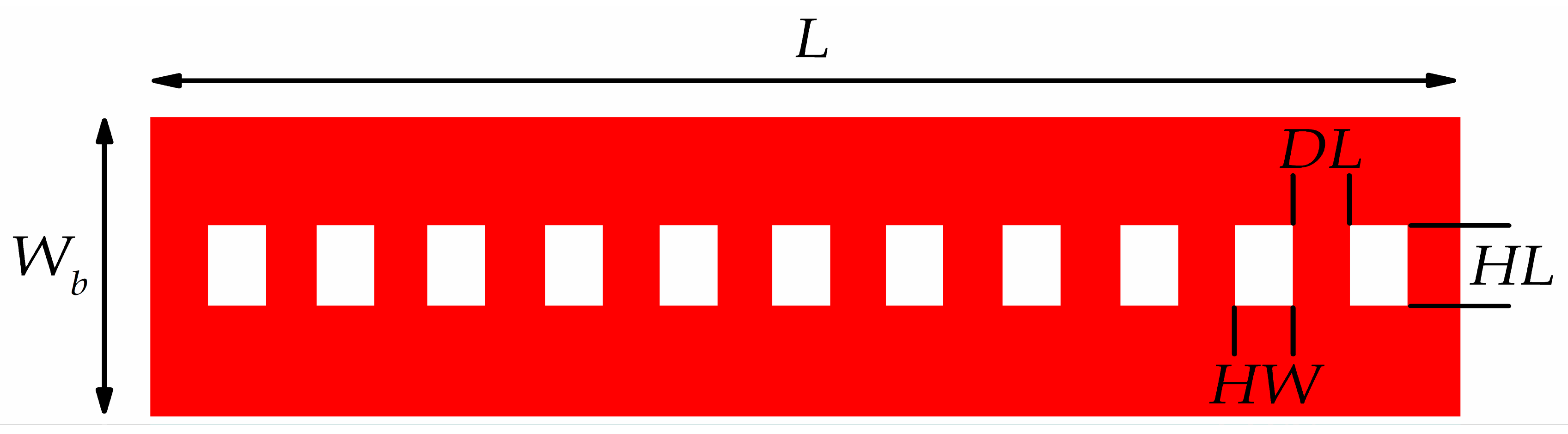
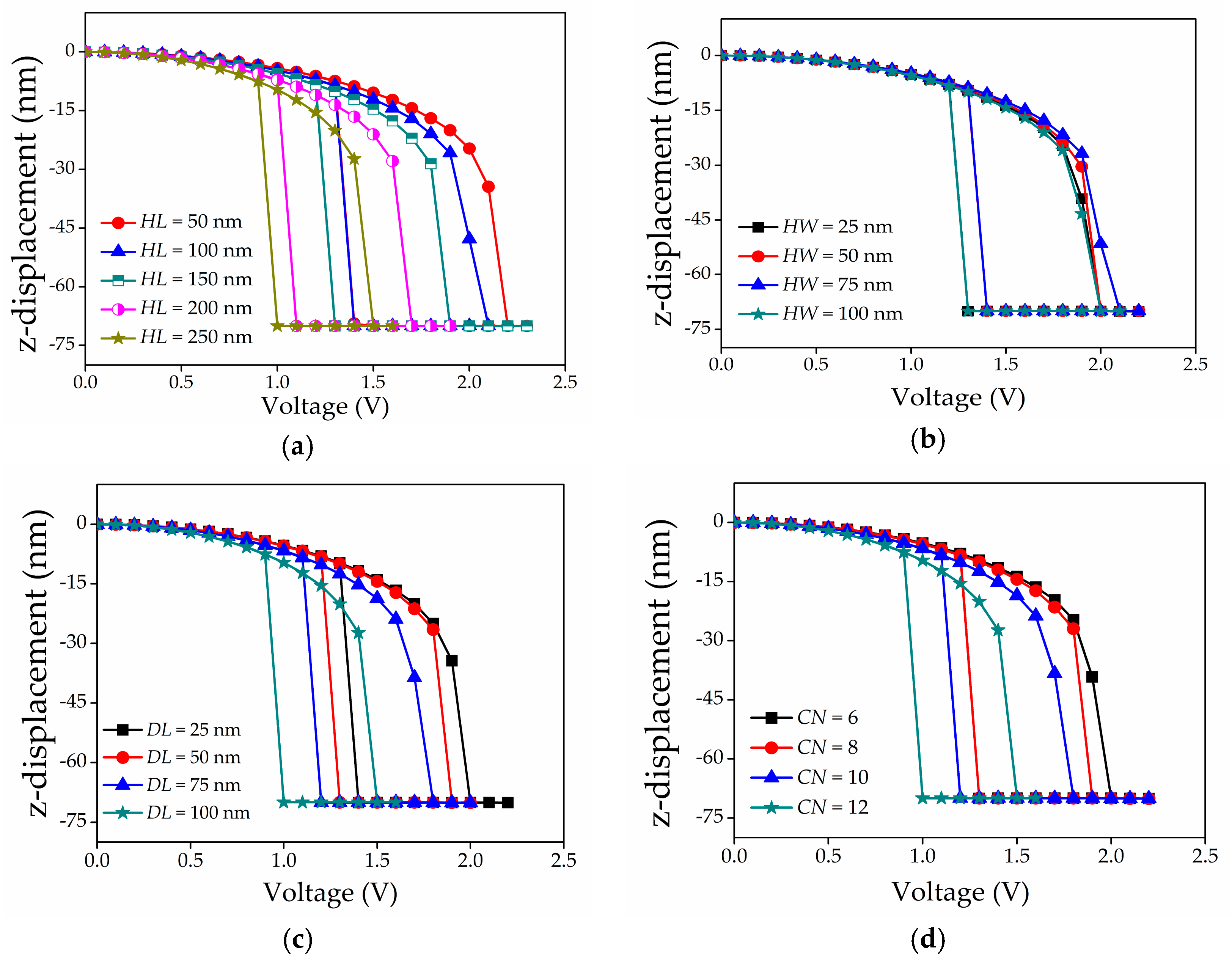
3.2. Analysis of Actuation Pull-In Voltage of the Perforated Graphene-Based NEM Switch
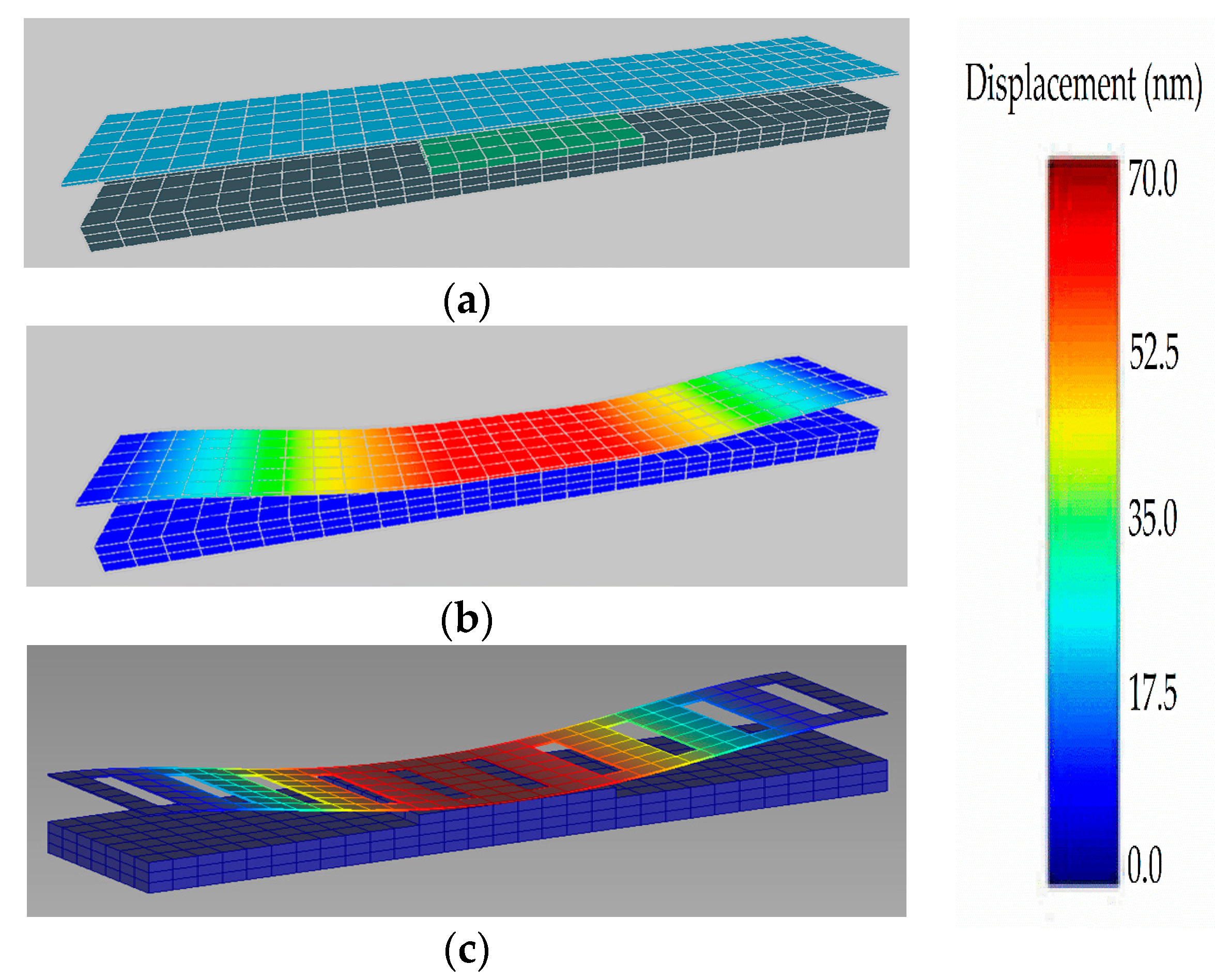
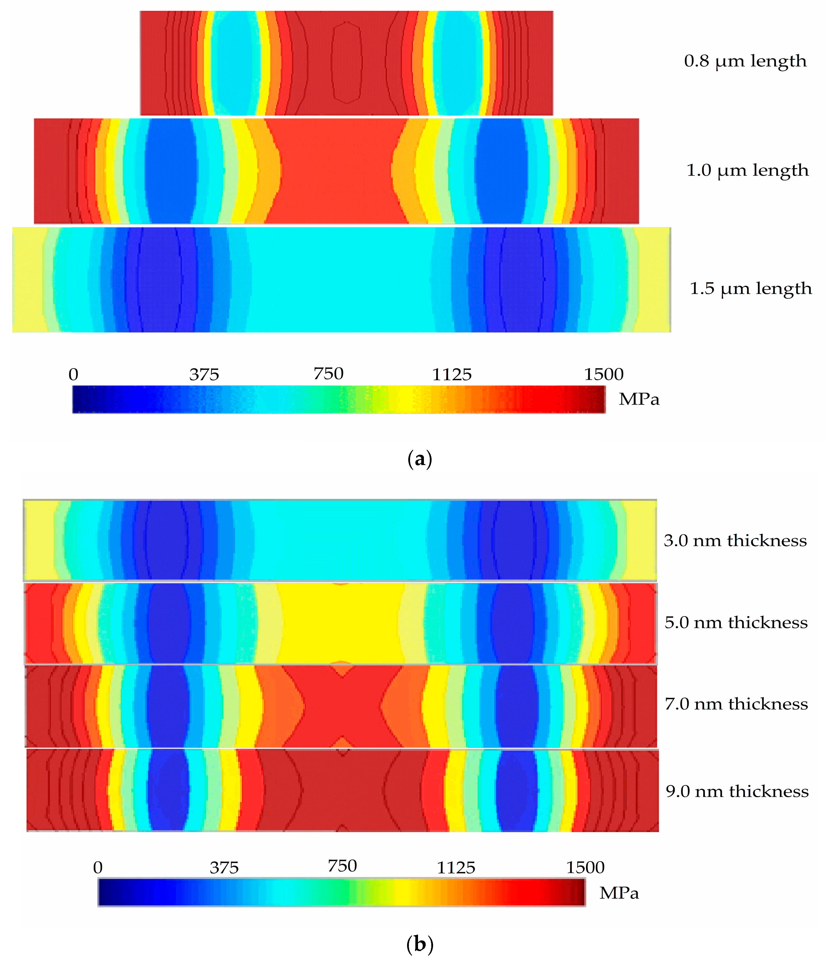
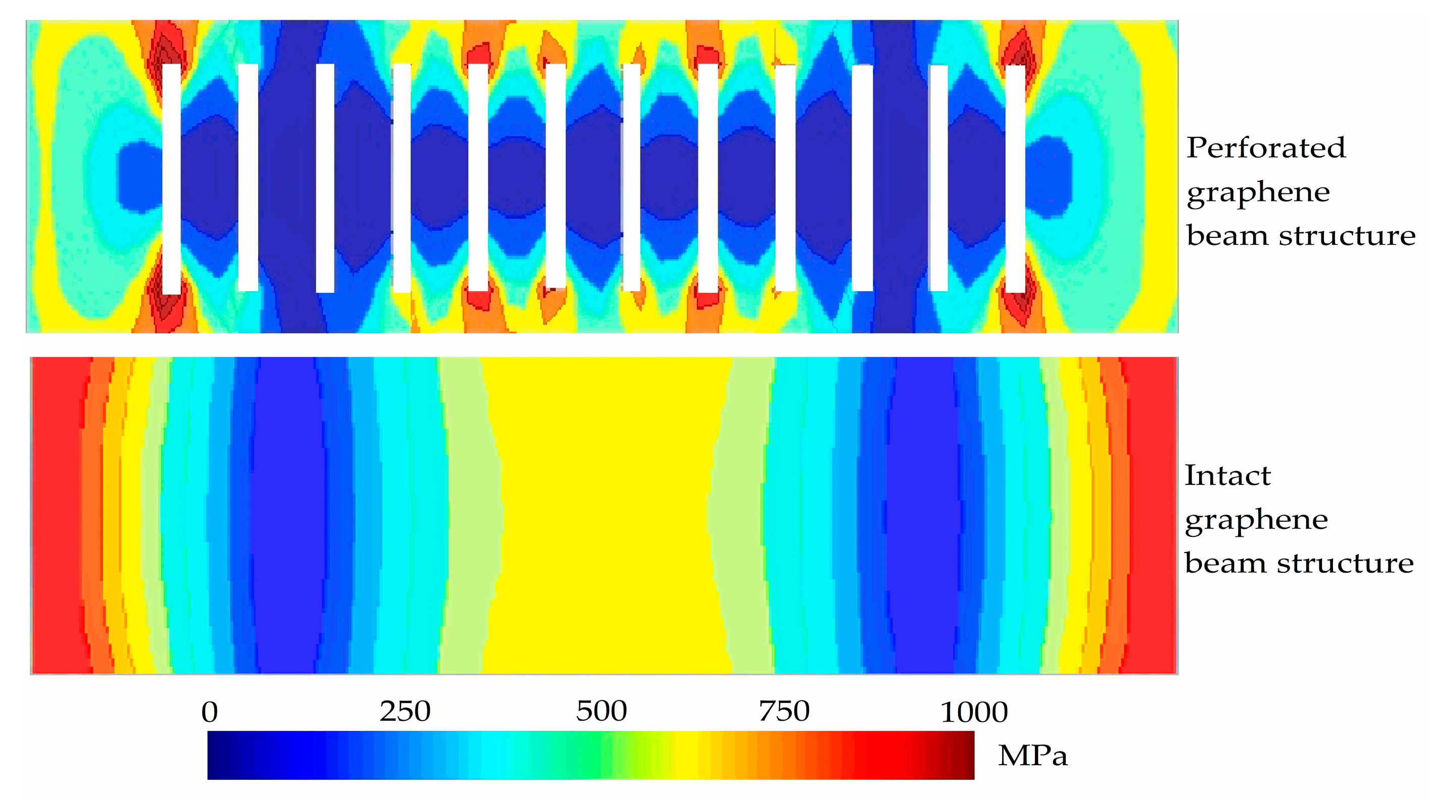
3.3. Analysis of Von Mises Stress
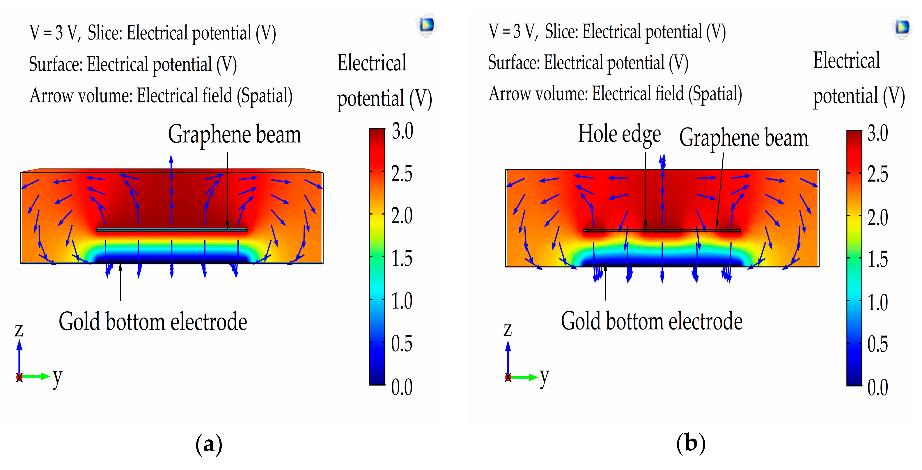
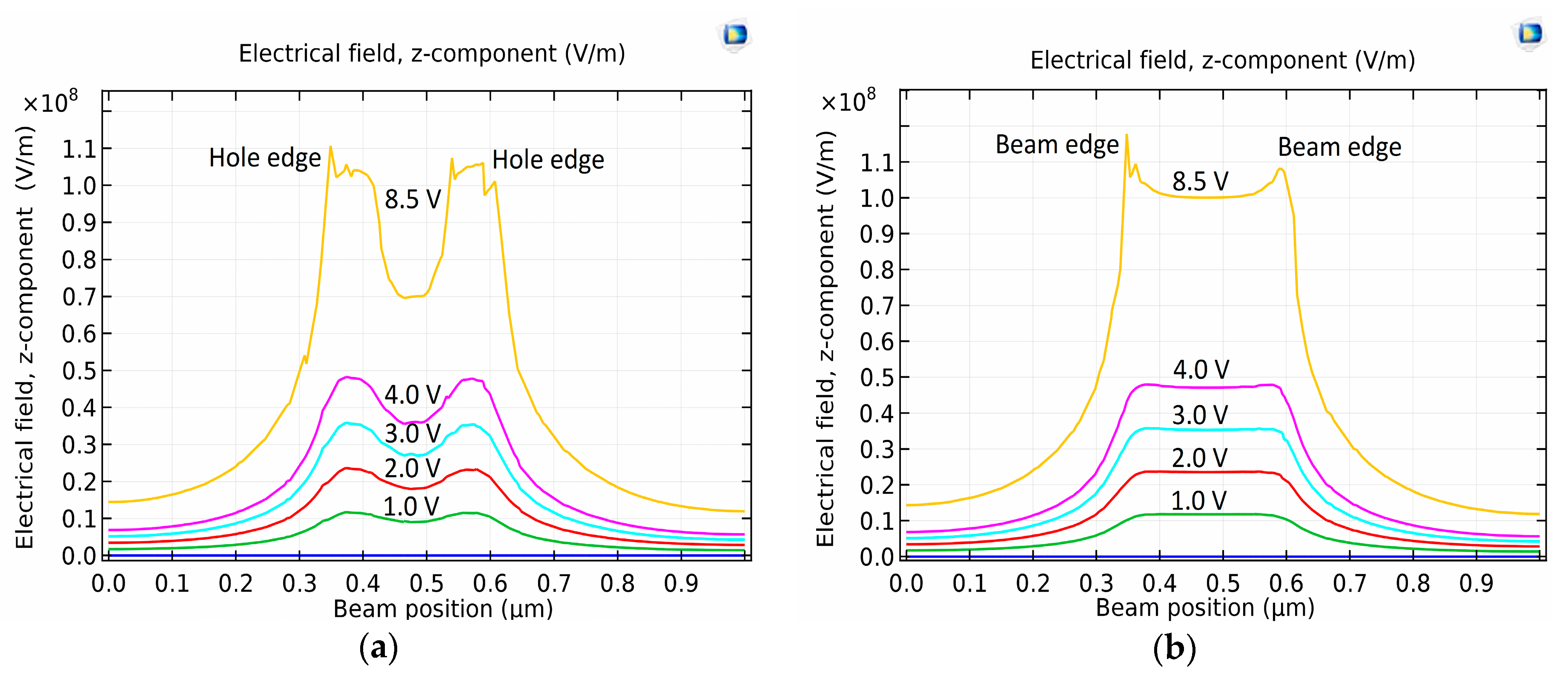
3.4. Analysis of Electrical Field Distribution
4. Conclusions
Acknowledgments
Author Contributions
Conflicts of Interest
References
- Peschot, A.; Qian, C.; Liu, T.-J.K. Nanoelectromechanical switches for low-power digital computing. Micromachines 2015, 6, 1046–1065. [Google Scholar] [CrossRef]
- Dadgour, H.F.; Banerjee, K. Design and analysis of hybrid NEMS-CMOS circuits for ultra-low power applications. In Proceedings of the 44th ACM/IEEE Design Automation Conference, San Diego, CA, USA, 4–8 June 2007; pp. 306–311. [Google Scholar]
- Kim, S.M.; Song, E.B.; Lee, S.; Seo, S.; Seo, D.H.; Hwang, Y.; Candler, R.; Wang, K.L. Suspended few-layer graphene beam electromechanical switch with abrupt on-off characteristics and minimal leakage current. Appl. Phys. Lett. 2011, 99, 15–17. [Google Scholar] [CrossRef]
- Han, M.Y.; Kim, P. Graphene nanoribbon devices at high bias. Nano Convergence 2014, 1, 1. [Google Scholar] [CrossRef] [PubMed]
- Li, P.; You, Z.; Haugstad, G.; Cui, T. Graphene fixed-end beam arrays based on mechanical exfoliation. Appl. Phys. Lett. 2011, 98, 253105. [Google Scholar] [CrossRef]
- Loh, O.Y.; Espinosa, H.D. Nanoelectromechanical contact switches. Nat. Nanotechnol. 2012, 7, 283–295. [Google Scholar] [CrossRef] [PubMed]
- Feng, X.L.; Matheny, M.H.; Zorman, C.A.; Mehregany, M.; Roukes, M.L. Low voltage nanoelectromechanical switches based on silicon carbide nanowires. Nano Lett. 2010, 10, 2891–2896. [Google Scholar] [CrossRef] [PubMed]
- Qian, Y.; Lou, L.; Tsai, M.J.; Lee, C. A dual-silicon-nanowires based U-shape nanoelectromechanical switch with low pull-in voltage. Appl. Phys. Lett. 2012, 100, 2010–2013. [Google Scholar] [CrossRef]
- Geim, A.K.; Novoselov, K.S. The rise of graphene. Nat. Mater. 2007, 6, 183–191. [Google Scholar] [CrossRef] [PubMed]
- Mizuno, N.; Nielsen, B.; Du, X. Ballistic-like supercurrent in suspended graphene Josephson weak links. Nat. Commun. 2013, 4, 2716. [Google Scholar] [CrossRef] [PubMed]
- Liu, X.; Suk, J.W.; Boddeti, N.G.; Cantley, L.; Wang, L.; Gray, J.M.; Hall, J.; Bright, V.M.; Rogers, C.T.; Dun, M.L.; et al. Large arrays and properties of 3-terminal graphene nanoelectromechanical switches. Adv. Mater. 2014, 26, 1571–1576. [Google Scholar] [CrossRef] [PubMed]
- Zulkefli, M.A.; Mohamed, M.A.; Siow, K.S.; Majlis, M.B. Optimization of beam length and air gap of suspended graphene NEMS switch for low pull-in voltage application. In Proceedings of the 2016 IEEE International Conference on Semiconductor Electronics (ICSE 2016), Kuala Lumpur, Malaysia, 17–19 August 2016; pp. 29–32. [Google Scholar]
- Sun, J.; Wang, W.; Muruganathan, M.; Mizuta, H. Low pull-in voltage graphene electromechanical switch fabricated with a polymer sacrificial spacer. Appl. Phys. Lett. 2014, 105, 33103. [Google Scholar] [CrossRef]
- Shi, Z.; Lu, H.; Zhang, L.; Yang, R.; Wang, Y.; Liu, D.; Guo, H.; Shi, D.; Gao, H.; Wang, E.; et al. Studies of graphene-based nanoelectromechanical switches. Nano Res. 2012, 5, 82–87. [Google Scholar] [CrossRef]
- Moldovan, C.F.; Vitale, W.A.; Sharma, P.; Bernard, L.S.; Ionescu, A.M. Fabrication process and characterization of suspended graphene membranes for RF NEMS capacitive switches. Microelectron. Eng. 2015, 145, 5–8. [Google Scholar] [CrossRef]
- Sun, J.; Muruganathan, M.; Kanetake, N.; Mizuta, H. Locally-actuated graphene-based nano-electro-mechanical switch. Micromachines 2016, 7, 124. [Google Scholar] [CrossRef]
- Saxena, A.; Agrawal, V.K. Comparative study of perforated RF MEMS switch. Procedia Comput. Sci. 2015, 57, 139–145. [Google Scholar] [CrossRef]
- Guha, K.; Kumar, M.; Agarwal, S.; Baishya, S. A modified capacitance model of RF MEMS shunt switch incorporating fringing field effects of perforated beam. Solid State Electron. 2015, 114, 35–42. [Google Scholar] [CrossRef]
- Shi, Z.; Yang, R.; Zhang, L.; Wang, Y.; Liu, D.; Shi, D.; Wang, E.; Zhang, G. Patterning graphene with zigzag edges by self-aligned anisotropic etching. Adv. Mater. 2011, 23, 3061–3065. [Google Scholar] [CrossRef] [PubMed]
- Sun, J.; Schmidt, M.E.; Muruganathan, M.; Chong, H.M.H.; Mizuta, H. Large-scale nanoelectromechanical switches based on directly deposited nanocrystalline graphene on insulating substrates. Nanoscale 2016, 8, 6659–6665. [Google Scholar] [CrossRef] [PubMed]
- Schmidt, M.E.; Xu, C.; Cooke, M.; Mizuta, H.; Chong, H.M.H. Metal-free plasma-enhanced chemical vapor deposition of large area nanocrystalline graphene. Mater. Res. Express 2014, 1, 25031. [Google Scholar] [CrossRef]
- Frank, I.W.; Tanenbaum, D.M.; van der Zande, A.M.; McEuen, P.L. Mechanical properties of suspended graphene sheets. J. Vac. Sci. Technol. B 2007, 25, 2558–2561. [Google Scholar] [CrossRef]
- Ma, J.B.; Jiang, L.; Asokanthan, S.F. Influence of surface effects on the pull-in stability of NEMS electrostatic switches. Nanotechnology 2010, 21, 505708. [Google Scholar] [CrossRef] [PubMed]
- Singh, T.; Khaira, N.K.; Sengar, J.S. Stress analysis using finite element modeling of a novel RF microelectromechanical system shunt switch designed on quartz substrate for low-voltage applications. Trans. Electr. Electron. Mater. 2013, 14, 225–230. [Google Scholar] [CrossRef]
- Zhang, W.-M.; Yan, H.; Peng, Z.-K.; Meng, G. Electrostatic pull-in instability in MEMS/NEMS: A review. Sens. Actuators Phys. 2014, 214, 187–218. [Google Scholar] [CrossRef]
- IntelliSense-Total MEMS Solutions-IntelliSuite Software. Available online: http://www.intellisense.com (accessed on 10 October 2016).
- Dequesnes, M.; Rotkin, S.V.; Aluru, N.R. Calculation of pull-in voltages for carbon-nanotube-based nanoelectromechanical switches. Nanotechnology 2002, 13, 120. [Google Scholar] [CrossRef]
- Bao, M.H. Micro Mechanical Transducers: Pressure Sensors, Accelerometers and Gyroscopes, 1st ed.; Elsevier: Oxford, UK, 2000; Chapter 4. [Google Scholar]
- Pilkey, W.D. Formulas for Stress, Strain, and Structural Matrices; John Wiley and Sons: New York, NY, USA, 1994. [Google Scholar]
- Bridgeman, T.; Chatwin, P.C.; Plumpton, C. Newton’s Laws and Particle Motion; Macmillan Education: London, UK, 1984. [Google Scholar]
- Beer, F. Mechanics of Materials, 2nd ed.; McGraw Hill: New York, NY, USA, 2002. [Google Scholar]
- Yung, W.C.; Budynas, R.G. Roak’s Formulas for Stress and Strain, 7th ed.; McGraw Hill: New York, NY, USA, 2002. [Google Scholar]
- Zulkefli, M.A.; Mohamed, M.A.; Siow, K.S.; Majlis, B.Y.; Kulothungan, J.; Muruganathan, M.; Mizuta, H. Stress analysis of perforated graphene nano-electro-mechanical (NEM) contact switches by 3D finite element simulation. Microsyst. Technol. 2017. [Google Scholar] [CrossRef]
- Kulothungan, J.; Muruganathan, M.; Mizuta, H. 3D finite element simulation of graphene nano-electro-mechanical switches. Micromachines 2016, 7, 143. [Google Scholar] [CrossRef]
- COMSOL Multiphysics® and COMSOL Server™. Available online: http://www.comsol.com (accessed on 10 October 2016).
- Kambali, P.N.; Pandey, A.K. Capacitance and Force Computation Due to Direct and Fringing Effects in MEMS/NEMS Arrays. IEEE Sens. J. 2016, 16, 375–382. [Google Scholar] [CrossRef]


| NEM Switch | Length, L (µm) | Thickness, t (nm) | Width, W (µm) | Air Gap Thickness, g (nm) | Pull-In Voltage (V) [20] | Pull-In Voltage (V) |
|---|---|---|---|---|---|---|
| i | 1.5 | 9.0 | 0.3 | 75 | 8.5 | 8.4 |
| ii | 1.0 | 50 | 15.0 | 17.4 | ||
| iii | 0.8 | 45 | 22.0 | 21.8 |
| NEM Switch | Remark | Length, L (µm) | Thickness, t (nm) | Air Gap Thickness, g (nm) | Width, Wb (µm) | Pull-In Voltage (V) |
|---|---|---|---|---|---|---|
| i | Length, L variation | 0.8 | 3 | 70 | 0.3 | 7.7 |
| ii | 1.0 | 5.0 | ||||
| iii | 1.5 | 2.2 | ||||
| iv | Thickness, t variation | 1.5 | 5 | 70 | 0.3 | 4.7 |
| v | 7 | 7.8 | ||||
| vi | 9 | 11.5 | ||||
| vii | Air gap, g variation | 1.5 | 3 | 100 | 0.3 | 3.4 |
| viii | 130 | 4.7 |
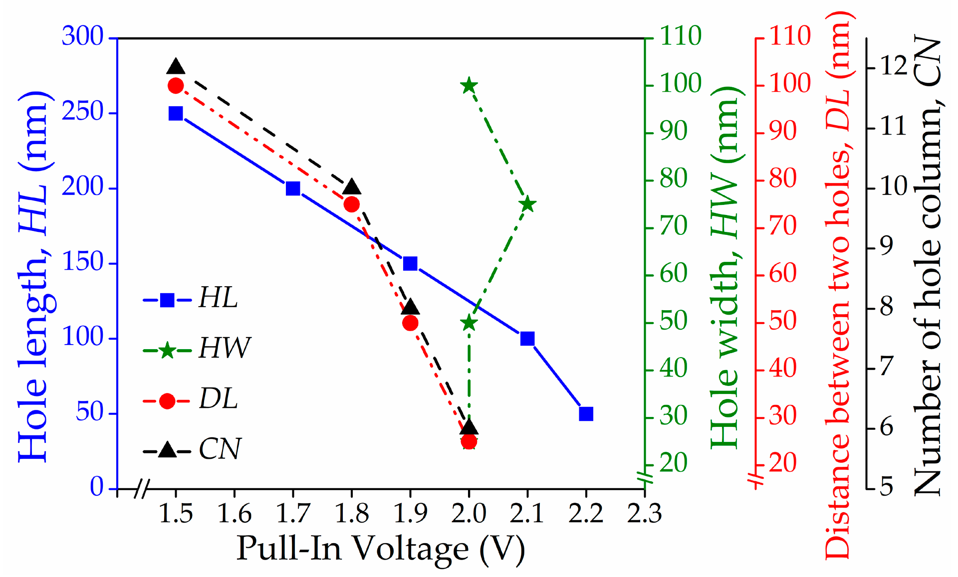
| NEM Switch | Remark | Hole Length, HL (nm) | Hole Width, HW (nm) | Distance between Each Hole, DL (nm) | Number of Hole Column, CN | Pull-In Voltage (V) | Pull-In Voltage (V) Analytical |
|---|---|---|---|---|---|---|---|
| A | Hole length, HL variation | 50 | 25 | 100 | 12 | 2.2 | 1.46 |
| B | 100 | 2.1 | 1.44 | ||||
| C | 150 | 1.9 | 1.43 | ||||
| D | 200 | 1.7 | 1.41 | ||||
| E | 250 | 1.5 | 1.39 | ||||
| F | Hole width, HW variation | 250 | 25 | 100 | 6 | 2.0 | 1.44 |
| G | 50 | 2.0 | 1.39 | ||||
| H | 75 | 2.1 | 1.36 | ||||
| I | 100 | 2.0 | 1.32 | ||||
| J | Distance between each hole, DL variation | 250 | 25 | 25 | 12 | 2.0 | N/A |
| K | 50 | 1.9 | |||||
| L | 75 | 1.8 | |||||
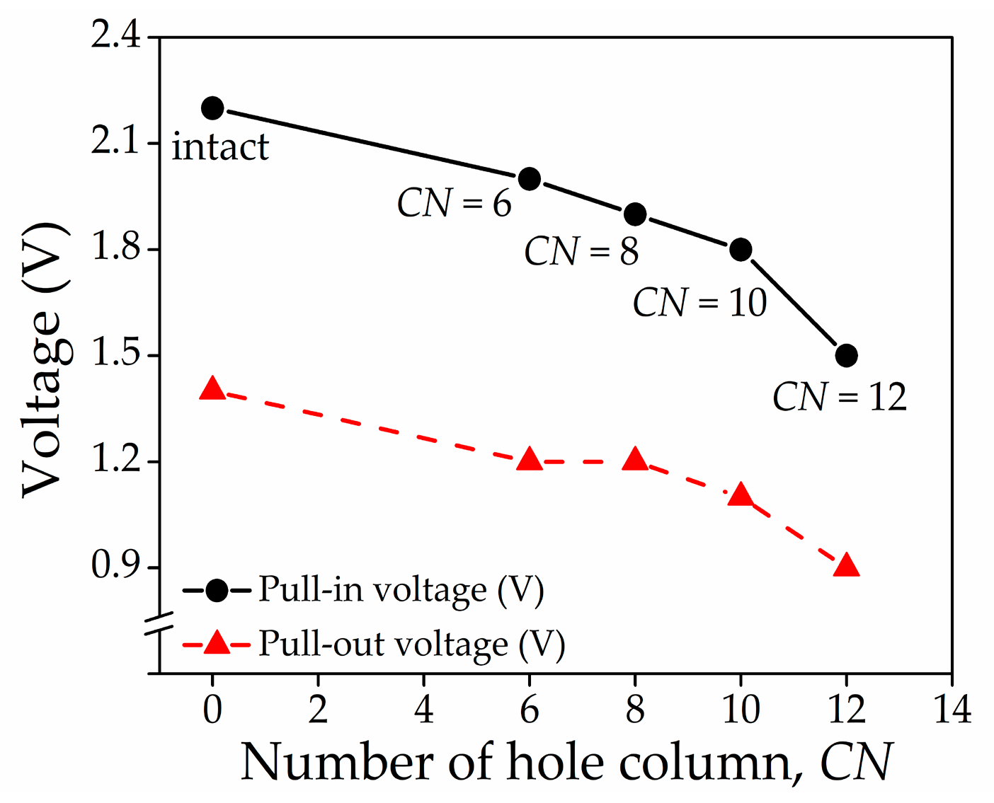
| M | Number of hole column, CN variation | 250 | 25 | 100 | 8 | 1.9 | 1.42 |
| N | 10 | 1.8 | 1.41 |
© 2017 by the authors. Licensee MDPI, Basel, Switzerland. This article is an open access article distributed under the terms and conditions of the Creative Commons Attribution (CC BY) license (http://creativecommons.org/licenses/by/4.0/).
Share and Cite
Zulkefli, M.A.; Mohamed, M.A.; Siow, K.S.; Yeop Majlis, B.; Kulothungan, J.; Muruganathan, M.; Mizuta, H. Three-Dimensional Finite Element Method Simulation of Perforated Graphene Nano-Electro-Mechanical (NEM) Switches. Micromachines 2017, 8, 236. https://doi.org/10.3390/mi8080236
Zulkefli MA, Mohamed MA, Siow KS, Yeop Majlis B, Kulothungan J, Muruganathan M, Mizuta H. Three-Dimensional Finite Element Method Simulation of Perforated Graphene Nano-Electro-Mechanical (NEM) Switches. Micromachines. 2017; 8(8):236. https://doi.org/10.3390/mi8080236
Chicago/Turabian StyleZulkefli, Mohd Amir, Mohd Ambri Mohamed, Kim S. Siow, Burhanuddin Yeop Majlis, Jothiramalingam Kulothungan, Manoharan Muruganathan, and Hiroshi Mizuta. 2017. "Three-Dimensional Finite Element Method Simulation of Perforated Graphene Nano-Electro-Mechanical (NEM) Switches" Micromachines 8, no. 8: 236. https://doi.org/10.3390/mi8080236