
Enhanced Sensitivity of MoTe2 Chemical Sensor through Light Illumination
by
 ,
,
Zhihong Feng
, 
Yuan Xie
,
Enxiu Wu
,
Yuanyuan Yu
,
Shijun Zheng
,
Rui Zhang
,
Xuejiao Chen
,
Chonglin Sun
*,
Hao Zhang
,
Wei Pang
,
Jing Liu
and
Daihua Zhang
* State Key Laboratory of Precision Measurement Technology and Instruments, School of Precision Instrument and Opto-Electronics Engineering, Tianjin University, No. 92 Weijin Road, Tianjin 300072, China
*
Authors to whom correspondence should be addressed.
Micromachines 2017, 8(5), 155; https://doi.org/10.3390/mi8050155
Submission received: 10 March 2017
/
Revised: 24 April 2017
/
Accepted: 10 May 2017
/
Published: 12 May 2017
(This article belongs to the Special Issue Nanomaterials Based Sensors)
Abstract
:Two-dimensional (2D) transition metal dichalcogenides (TMDCs) semiconducting materials have recently attracted wide attention and been regarded as promising building blocks for chemical sensors due to their high surface-to-volume ratio. However, their low response hinders the realization of high-performance 2D TMDCs chemical sensors. Here, we demonstrate the improvement of sensing performance of molybdenum ditelluride (MoTe2) gas sensor through continuous light illumination. The dependence of sensing performance on the energy of photons and light intensity is systematically studied. The response to NH3 is dramatically enhanced by more than 25 times under 254 nm ultraviolet (UV) light illumination with intensity of 2.5 mW/cm2. Moreover, a remarkable low detection limit of 3 ppb is achieved, which is improved by 80 times compared with that in dark condition. The results demonstrate that light illumination is a promising method to improve the sensitivity of 2D TMDCs chemical sensors.
1. Introduction
Detecting ultra-low concentration of toxic and harmful gases has become more and more important in many promising applications such as environmental monitoring, industrial manufacturing and diagnostic processes, etc. [1]. In particular, semiconductor chemical sensors have attracted considerable attention owing to their low cost, ease of integration and simple sensing mechanism based on the conductance change upon gas exposure [2]. Over the past few decades, metal oxide semiconductor sensors have delivered satisfactory sensitivity in many cases [3,4,5], however, they require very high temperature (generally above 200 °C) to activate the chemisorption of atmospheric oxygen on the metal oxide surface, which raises several thermal-related issues and restricts their applications in oxygen-free environments or hazardous environments containing flammable gas species. Therefore, highly-sensitive chemical sensors which can operate at room temperature are highly desired. Recently, semiconducting two-dimensional (2D) transition metal dichalcogenides (TMDCs) have been widely studied and considered as promising gas-sensing materials due to their high surface-to-volume ratio and favorable surface energy level for gas adsorption [6,7,8,9,10]. Besides, researchers have also developed various approaches, for instance, surface functionalization [11] and using vertically aligned structure [12] to further enhance the sensitivity of 2D TMDCs based chemical sensors. However, the results show limited improvement, which is usually less than 10 times. Illuminating sensors with light is another effective way to dramatically improve the performance of semiconductor chemical sensors [13,14,15]. However, few have systematically investigated the influence of light illumination on the performance of 2D TMDCs based sensors.
Molybdenum ditelluride (MoTe2), a new addition to the class of 2D TMDCs, has a smaller band gap of ~1.0 eV compared with other TMDCs, which extends the photo detection range of TMDCs based phototransistor from the visible to near-infrared range [16]. Recent experimental investigations show that MoTe2 photodetector has a high photoresponsivity and a fast photoresponse in broad spectral range [17,18]. In the view of growing attention on MoTe2 for possible optoelectronic device applications, it is also important to investigate the influence of light illumination on the sensing performance of MoTe2 based chemical sensors.
In this work, we report the improvement of gas-sensing properties of MoTe2 chemical sensor through light illumination. The sensitivity of MoTe2 sensor for NH3 detection was enhanced by more than 25 times and the detection limit as low as 3 ppb was achieved under continuous ultraviolet (UV) light illumination. The influences of wavelength and intensity of light on the improvement of the sensing properties have also been systematically studied.
2. Materials and Methods
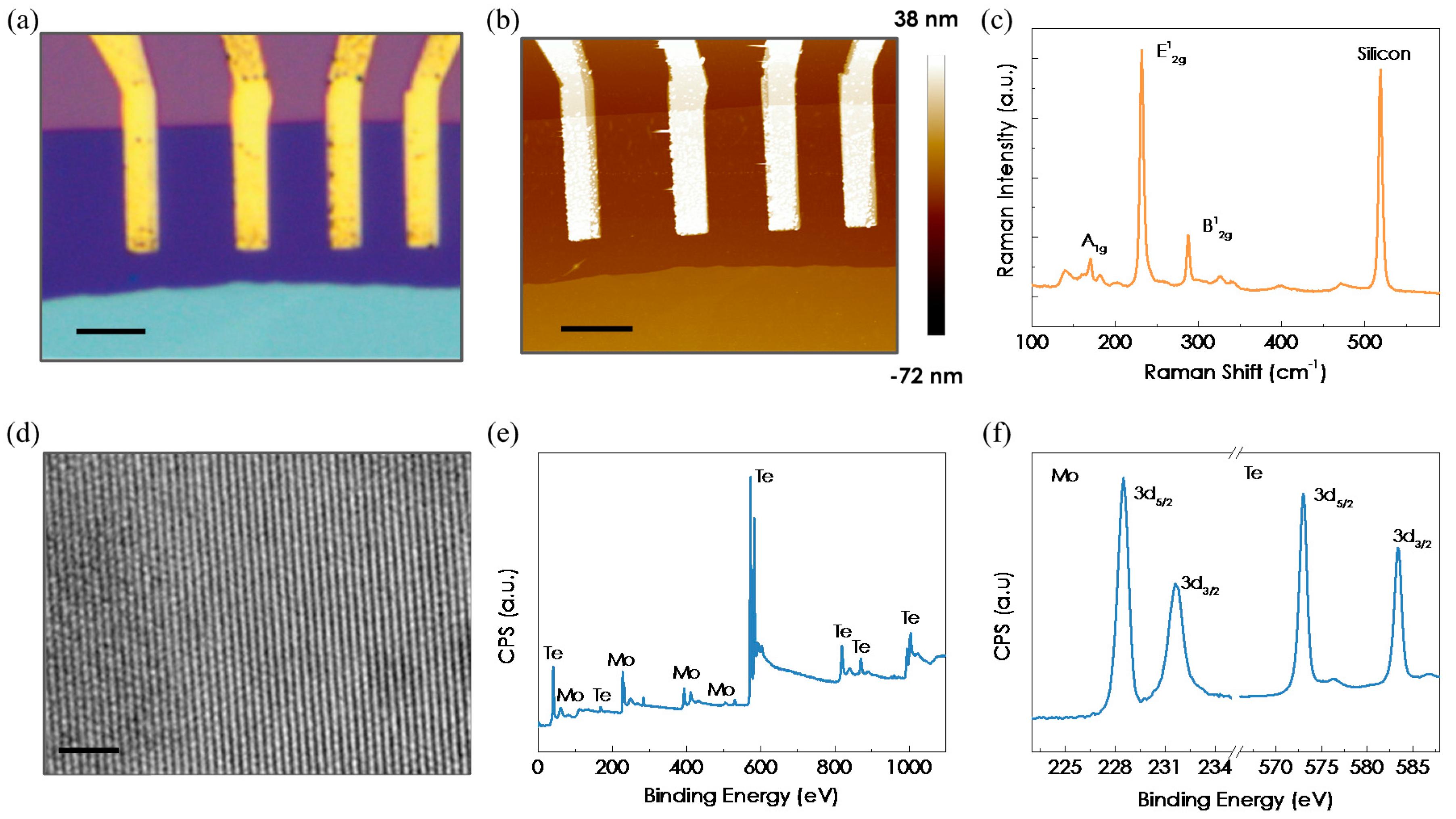
Few-layered MoTe2 flakes were prepared by mechanical exfoliation of a MoTe2 bulk crystal on n+ doped silicon substrate covered with 285 nm of thermally grown SiO2. The tape residues after exfoliation were removed by dipping the substrate along with flakes in acetone for 10 min. The electrical contacts on MoTe2 were fabricated by lift-off process using electron beam lithography and subsequent electron beam evaporation of 20/60 nm Ti/Au. Figure 1a shows the optical microscope image of a typical fabricated MoTe2 field-effect transistor (FET) device. Thickness of the MoTe2 flake is 3.4 nm, as confirmed by the atomic force microscopy (AFM, Bruker, Santa Barbara, CA, USA) measurement shown in Figure 1b. MoTe2 has two stable crystal phases: semiconducting 2H (hexagonal) and metallic 1T′ (distorted octahedral) phases [19]. Density functional theory (DFT) calculations revealed that molecular adsorption favors semiconducting 2H phase other than 1T′ metallic phase [20]. So it is important to determine the exact crystal structure of the MoTe2 flakes we used. Figure 1c shows the Raman spectra (532 nm excitation wavelength) for the exfoliated few-layered MoTe2. The characteristic Raman-active modes of the out-of-plane A1g mode at 170 cm−1, prominent in-plane E12g mode at 231 cm−1 and the out-of-plane B12g mode at 287 cm−1 are clearly observed. These Raman features are signature peak positions of 2H phase MoTe2 and in good agreement with the results reported previously [19]. The crystallographic structure of the MoTe2 was further characterized by high-resolution transmission electron microscopy (TEM, JEOL, Tokyo, Japan). Figure 1d shows a typical TEM image of as-exfoliated MoTe2 film. We could clearly observe a high level of crystallinity and hexagonal symmetry. X-ray photoelectron spectroscopy (XPS, PerkinElmer, Waltham, MA, USA) was utilized to determine the elemental composition and bonding types of the MoTe2 flakes. The XPS spectrum displayed in Figure 1e reveals the presence of Mo and Te elements in the flakes. Peaks are observed at 228.4, 231.5, 573 and 583.4 eV, corresponding to the Mo 3d5/2, Mo 3d3/2, Te 3d5/2 and Te 3d3/2, respectively, as shown in Figure 1f. These features are consistent with previous results from 2H MoTe2 [16].
3. Results and Discussion
We then investigate the effect of UV light illumination on the electrical performance of the MoTe2 FET device in pure N2 (99.9999%) environment. The wavelength of UV light source is 254 nm and the intensity is 2.5 mW/cm2. Figure 2a shows the transfer characteristics of the MoTe2 FET device in both linear and semi-log scales under dark condition. The device shows ambipolar behavior with a minimum current around Vgs = −18 V. The Ids increases dramatically by 2 × 10³ when Vgs increases from −18 V to 30 V, indicating electron accumulation in the MoTe2 channel. When Vgs decreases from −18 V to −30 V, the Ids is dominated by holes, as evidenced by increasing Ids. The observation is also consistent with previous studies [21]. After UV light illumination for 2 h, we note that the p-type behavior vanishes and the MoTe2 FET device behaves as n-type transistor as evidenced in the Ids–Vgs curves in Figure 2b. When Vgs increases from −30 to 30 V, Ids increases monotonically by more than 3 orders of magnitude due to accumulation of electrons in the conduction channel. The vanished p-type behavior of the MoTe2 FET under UV light illumination can be attributed to the removal of O2 molecules from MoTe2 flake. This can also be confirmed by the reversible electrical characteristics of one MoTe2 FET (Figure S1). The oxygen molecules adsorbed on the surface of MoTe2 flake may act as acceptors which induce p-type doping [22].
We then carried out systematic sensing tests of the MoTe2 FET toward NH3 in both dark and light illumination conditions to characterize its sensing performance at room temperature. Prior to the sensing experiments, the gas chamber and device were purged with N2 for 2 h under UV light illumination. N2 was used as the carrying gas to dilute the target gases to desired concentrations through flow rate adjustments. The gate electrode is grounded throughout all measurements.
Figure 3a presents the real time response of the MoTe2 sensor toward exposure of NH3 from 300 ppb to 30 ppm under both dark and light illumination conditions. The light intensity was kept at 2.5 mW/cm2. The device conductance increases monotonically with increasing NH3 concentrations for all conditions as NH3 molecules adsorption increase the electron concentration in the n-type semiconducting channel. The response is defined as (G − G0)/G0 × 100%, where G0 and G are the initial conductance and 5 min after NH3 exposure, respectively. We note that the response of the MoTe2 sensor is enhanced remarkably under light illumination from near-infrared to UV region. For example, the device shows responses ranging from ~4 to 25% under dark condition, whereas it presents larger responses ranging from ~100 to 790% under 254 nm UV light illumination at NH3 concentrations of 300 ppb–30 ppm. Therefore, the response is enhanced by more than 25 times by UV light illumination. The response values obtained under UV light illumination are well above the results from 2D TMDCs chemical sensors for NH3 detection. For comparison, the study in [9] and [23] demonstrated sensitivity of MoSe2 and WS2 sensors from a few to tens of ppm concentrations. It is noteworthy that for the MoS2 sensor with a lower detection limit down to 300 ppb, the response is ~0.04% [24], which is 3 orders lower than the MoTe2 sensor. By comparing the data points at different concentrations of NH3 under light illumination with different wavelength, we also note that the sensitivity enhancement increases monotonically with reducing wavelength (increasing photon energy), as shown in Figure 3b. The sensitivity improvement is 2–6-fold in the near-infrared to red region, while it increases to more than 10 times in the UV region. The largest sensitivity enhancement is achieved under 254 nm UV light illumination. The enhanced sensitivity under light illumination can be attributed to the following reasons: The presence of defects in MoTe2 during the crystal growth process can act as active sites. Density functional theory calculations revealed that the presence of defects strongly increases the binding energy of the molecular interaction on MoTe2 surface [25,26]. For example, interaction at the defect sites, such as Te vacancies, yields much larger binding energy between MoTe2 and O2 (~166 meV) compared to the case of pure MoTe2 (~36–64 meV) [25]. The O2 molecules initially adsorbed on the surface of MoTe2 may occupy the defect sites. Therefore, removal of O2 molecules could significantly enhance the sensitivity. However, the thermal energy at room temperature could not desorb O2 molecules [27,28]. In this respect, UV illumination can provide the energy for O2 desorption through several mechanisms [29,30]. The study in Reference 29 suggested that photo induced desorption strongly depends on the wavelength of light. UV light illumination has the highest efficiency for “cleaning” the nanomaterial surface owing to electron plasmon excitation. Therefore, the best sensitivity was achieved under UV light illumination. By comparing the response time and recovery rate in dark and light illumination conditions (Figure S2), we also note that the response time is not changed too much while the recovery rate is slower under light illumination than that in dark. This can be attributed to the following reason: NH3 molecules are mainly adsorbed on the pristine surface of MoTe2 due to occupancy of active sites by O2 molecules in dark condition. Under light illumination, the active sites are released and the binding energy between NH3 and active sites are much higher than the pristine case. On the other hand, we also note that the recovery rate is faster in the UV region than in the near-infrared to red region. Under UV light illumination, the desorption rate of NH3 from active sites is increased due to electron plasmon excitation [29] so that a dynamic equilibrium is established between adsorption and desorption processes.
Figure 3c plots the response as a function of NH3 concentration in the dark and under light illumination. The response is linear at low concentrations and shows a quasi-saturation behavior as the concentration increases. The linear portion of the curve can be then used to estimate the detection limit, which is typically defined as the concentration level corresponding to a signal-to-noise ratio (SNR) of 3 [31]. Under 254 nm UV light illumination, the detection limit is estimated to be ~3 ppb by comparing the noise level (0.17%) of the sensor to the slope (196% ppm−1) of the response at low concentration of NH3. This number is 80 times superior to that in the dark, which is estimated to be ~243 ppb according to the slope of the response (Figure 3d). We also note the detection limit of our MoTe2 sensor under 254 nm UV light illumination is the record number using 2D TMDCs so far [6,7,9,23,24,32,33] and competitive with other nano-sensors [34,35,36].
Figure 4a shows the dynamic response of the MoTe2 sensor to different NH3 concentrations (300 ppb–30 ppm) under UV light illumination (254 nm) with intensity ranging from 0.25 to 2.5 mW/cm2. We note that the sensing properties of the MoTe2 sensor behave similar but the responses are strongly influenced by the light intensity. For example, the response to 30 ppm NH3 is ~290% at intensity of 0.25 mW/cm2, while it increases up to ~790% at intensity of 2.5 mW/cm2. Figure 4b presents the dependence of the response on the UV light intensity. The response increases rapidly when the intensity increases from 0.25 to 1 mW/cm2 and then shows slow saturation trend as the intensity increases up to 2.5 mW/cm2, the highest intensity we could experimentally achieve with the setup. Generally, the light intensity should have an optimal value for maximum sensitivity as the desorption rate will increase more than the adsorption rate if the intensity is too high [37]; however, we did not observe this phenomena due to the limited power density of our light source. The detection limit is also improved with higher light intensity. The slopes of the response plotted in Figure 4c are 196% ppm−1 and 90.4% ppm−1 at intensity of 2.5 and 0.25 mW/cm2, respectively, from which we can obtain a detection limit of ~3 and 6 ppb, respectively. Therefore, the detection limit is improved by 2-fold as the intensity increases by 10 times.
4. Conclusions
In summary, we report a systematic study on the sensitivity enhancement of MoTe2 gas sensor through light illumination. Compared with dark conditions, the sensitivity is dramatically improved by light illumination and monotonically dependent on the photon energy. With continuous 254 nm UV light illumination, the response to NH3 gas is enhanced by more than 25 times and a detection limit as low as 3 ppb is achieved. It is also found that the enhanced sensitivity is dependent on the light intensity. The response increases from 290 to 790% at 30 ppm NH3 when increasing the UV light intensity from 0.25 to 2.5 mW/cm2. Our results prove a strong influence of light illumination on the sensitivity of MoTe2 sensor and demonstrate the potential of 2D MoTe2 as a promising candidate for ultrasensitive chemical sensing applications.
Supplementary Materials
The following are available online at www.mdpi.com/2072-666X/8/5/155/s1, Figure S1: Transfer characteristics of MoTe2 FET (a) before and (b) after UV illumination and (c) after recovery in air. (d–f) Corresponding output characteristics in (a–c). Figure S2: (a) Response time of the MoTe2 sensor under different condition. (b) Recovery of the MoTe2 sensor under different condition. The response time was defined as the time required to change the conductance after exposure of NH3 in a specific range of 90%. The recovery was defined as (G − G10min)/(G − G0) × 100%, where G0 and G are the initial conductance and 5 min after NH3 exposure, respectively, 𝐺10min is the device conductance after shutting off the target gas for 10 min.
Acknowledgments
Daihua Zhang acknowledges support by the Tianjin Applied Basic Research and Advanced Technology (13JKYBJC37100). This work was financially supported the 111 Project (B07014).
Author Contributions
Zhihong Feng and Yuan Xie designed and performed the experiments. Daihua Zhang and Zhihong Feng analyzed the data and wrote the paper. Enxiu Wu, Yuanyuan Yu, Shijun Zheng and Rui Zhang provided advices on experiment design and data analysis. Xuejiao Chen, Chonglin Sun, Hao Zhang, Wei Pang and Jing Liu attended the discussion of the data analysis. All authors have read and approved the final manuscript.
Conflicts of Interest
The authors declare no conflict of interest.
References
- Wang, F.; Wang, L.; Chen, X.; Yoon, J. Recent progress in the development of fluorometric and colorimetric chemosensors for detection of cyanide ions. Chem. Soc. Rev. 2014, 43, 4312–4324. [Google Scholar] [CrossRef] [PubMed]
- Tricoli, A.; Righettoni, M.; Teleki, A. Semiconductor gas sensors: Dry synthesis and application. Angew. Chem. Int. Ed. Engl. 2010, 49, 7632–7659. [Google Scholar] [CrossRef] [PubMed]
- Miller, D.R.; Akbar, S.A.; Morris, P.A. Nanoscale metal oxide-based heterojunctions for gas sensing: A review. Sens. Actuators B Chem. 2014, 204, 250–272. [Google Scholar] [CrossRef]
- Shao, F.; Hoffmann, M.W.G.; Prades, J.D.; Zamani, R.; Arbiol, J.; Morante, J.R.; Varechkina, E.; Rumyantseva, M.; Gaskov, A.; Giebelhaus, I.; et al. Heterostructured p-CuO (nanoparticle)/n-SnO2 (nanowire) devices for selective H2S detection. Sens. Actuators B Chem. 2013, 181, 130–135. [Google Scholar] [CrossRef]
- Li, J.; Liu, X.; Cui, J.; Sun, J. Hydrothermal synthesis of self-assembled hierarchical tungsten oxides hollow spheres and their gas sensing properties. ACS Appl. Mater. Interfaces 2015, 7, 10108–10114. [Google Scholar] [CrossRef] [PubMed]
- Late, D.J.; Huang, Y.K.; Liu, B.; Acharya, J.; Shirodkar, S.N.; Luo, J.; Yan, A.; Charles, D.; Waghmare, U.V.; Dravid, V.P.; et al. Sensing behavior of atomically thin-layered MoS2 transistors. ACS Nano 2013, 7, 4879–4891. [Google Scholar] [CrossRef] [PubMed]
- Liu, B.; Chen, L.; Liu, G.; Abbas, A.N.; Fathi, M.; Zhou, C. High-performance chemical sensing using Schottky-contacted chemical vapor deposition grown monolayer MoS2 transistors. ACS Nano 2014, 8, 5304–5314. [Google Scholar] [CrossRef] [PubMed]
- Perkins, F.K.; Friedman, A.L.; Cobas, E.; Campbell, P.M.; Jernigan, G.G.; Jonker, B.T. Chemical vapor sensing with monolayer MoS2. Nano Lett. 2013, 13, 668–673. [Google Scholar] [CrossRef] [PubMed]
- Late, D.J.; Doneux, T.; Bougouma, M. Single-layer MoSe2 based NH3 gas sensor. Appl. Phys. Lett. 2014, 105. [Google Scholar] [CrossRef]
- Tong, Y.; Lin, Z.H.; Thong, J.T.L.; Chan, D.S.H.; Zhu, C.X. MoS2 oxygen sensor with gate voltage stress induced performance enhancement. Appl. Phys. Lett. 2015, 107, 123105. [Google Scholar] [CrossRef]
- Ko, K.Y.; Song, J.G.; Kim, Y.; Choi, T.; Shin, S.; Lee, C.W.; Lee, K.; Koo, J.; Lee, H.; Kim, J.; et al. Improvement of Gas-Sensing Performance of Large-Area Tungsten Disulfide Nanosheets by Surface Functionalization. ACS Nano 2016, 10, 9287–9296. [Google Scholar] [CrossRef] [PubMed]
- Cho, S.Y.; Kim, S.J.; Lee, Y.; Kim, J.S.; Jung, W.B.; Yoo, H.W.; Kim, J.; Jung, H.T. Highly Enhanced Gas Adsorption Properties in Vertically Aligned MoS2 Layers. ACS Nano 2015, 9, 9314–9321. [Google Scholar] [CrossRef] [PubMed]
- Park, S.; An, S.; Ko, H.; Lee, S.; Lee, C. Synthesis, structure, and UV-enhanced gas sensing properties of Au-functionalized ZnS nanowires. Sens. Actuators B Chem. 2013, 188, 1270–1276. [Google Scholar] [CrossRef]
- Park, S.; An, S.; Mun, Y.; Lee, C. UV-enhanced NO2 gas sensing properties of SnO2-core/ZnO-shell nanowires at room temperature. ACS Appl. Mater. Interfaces 2013, 5, 4285–4292. [Google Scholar] [CrossRef] [PubMed]
- Ho, Y.; Huang, W.; Chang, H.; Wei, P. Ultraviolet-enhanced room-temperature gas sensing by using floccule-like zinc oxide nanostructures. Appl. Phys. Lett. 2015, 106, 183103. [Google Scholar] [CrossRef]
- Zhou, L.; Xu, K.; Zubair, A.; Liao, A.D.; Fang, W.; Ouyang, F.; Lee, Y.H.; Ueno, K.; Saito, R.; Palacios, T.; et al. Large-Area Synthesis of High-Quality Uniform Few-Layer MoTe2. J. Am. Chem. Soc. 2015, 137, 11892–11895. [Google Scholar] [CrossRef] [PubMed]
- Yin, L.; Zhan, X.; Xu, K.; Wang, F.; Wang, Z.; Huang, Y.; Wang, Q.; Jiang, C.; He, J. Ultrahigh sensitive MoTe2 phototransistors driven by carrier tunneling. Appl. Phys. Lett. 2016, 108, 043503. [Google Scholar] [CrossRef]
- Octon, T.J.; Nagareddy, V.K.; Russo, S.; Craciun, M.F.; Wright, C.D. Fast High-Responsivity Few-Layer MoTe2 Photodetectors. Adv. Opt. Mater. 2016, 4, 1750–1754. [Google Scholar] [CrossRef]
- Cho, S.; Kim, S.; Kim, J.H.; Zhao, J.; Seok, J.; Keum, D.H.; Baik, J.; Choe, D.-H.; Chang, K.J.; Suenaga, K.; et al. Phase patterning for ohmic homojunction contact in MoTe2. Science 2015, 349, 625–628. [Google Scholar] [CrossRef] [PubMed]
- Zhou, Y.; Reed, E.J. Structural Phase Stability Control of Monolayer MoTe2 with Adsorbed Atoms and Molecules. J. Phys. Chem. C 2015, 119, 21674–21680. [Google Scholar] [CrossRef]
- Xu, H.; Fathipour, S.; Kinder, E.W.; Seabaugh, A.C.; Fullerton-shirey, S.K. Reconfigurable Ion Gating of 2H-MoTe2 Field-Effect Transistors Using Poly(ethylene oxide)-CsClO4 Solid Polymer Electrolyte. ACS Nano 2015, 9, 4900–4910. [Google Scholar] [CrossRef] [PubMed]
- Cho, K.; Park, W.; Park, J.; Jeong, H.; Jang, J.; Kim, T.Y.; Hong, W.K.; Hong, S.; Lee, T. Electric stress-induced threshold voltage instability of multilayer MoS2 field effect transistors. ACS Nano 2013, 7, 7751–7758. [Google Scholar] [CrossRef] [PubMed]
- O’Brien, M.; Lee, K.; Morrish, R.; Berner, N.C.; McEvoy, N.; Wolden, C.A.; Duesberg, G.S. Plasma assisted synthesis of WS2 for gas sensing applications. Chem. Phys. Lett. 2014, 615, 6–10. [Google Scholar]
- Lee, K.; Gatensby, R.; McEvoy, N.; Hallam, T.; Duesberg, G.S. High-performance sensors based on molybdenum disulfide thin films. Adv. Mater. 2013, 25, 6699–6702. [Google Scholar] [CrossRef] [PubMed]
- Chen, B.; Sahin, H.; Suslu, A.; Ding, L.; Bertoni, M.I.; Peeters, F.M.; Tongay, S. Environmental changes in MoTe2 excitonic dynamics by defects-activated molecular interaction. ACS Nano 2015, 9, 5326–5332. [Google Scholar] [CrossRef] [PubMed]
- Zhang, Y.-H.; Chen, Y.-B.; Zhou, K.-G.; Liu, C.-H.; Zeng, J.; Zhang, H.-L.; Peng, Y. Improving gas sensing properties of graphene by introducing dopants and defects: A first-principles study. Nanotechnology 2009, 20, 185504. [Google Scholar] [CrossRef] [PubMed]
- Iqbal, M.W.; Iqbal, M.Z.; Jin, X.; Hwang, C.; Eom, J. Edge oxidation effect of chemical-vapor-deposition-grown graphene nanoconstriction. ACS Appl. Mater. Interfaces 2014, 6, 4207–4213. [Google Scholar] [CrossRef] [PubMed]
- Iqbal, M.W.; Iqbal, M.Z.; Khan, M.F.; Shehzad, M.A.; Seo, Y.; Eom, J. Deep-ultraviolet-light-driven reversible doping of WS2 field-effect transistors. Nanoscale 2014, 7, 747–757. [Google Scholar] [CrossRef] [PubMed]
- Chen, R.J.; Franklin, N.R.; Kong, J.; Cao, J.; Tombler, T.W.; Zhang, Y.; Dai, H. Molecular photodesorption from single-walled carbon nanotubes. Appl. Phys. Lett. 2001, 79, 2258–2260. [Google Scholar] [CrossRef]
- Law, M.; Kind, H.; Messer, B.; Kim, F.; Yang, P. Photochemical sensing of NO2 with SnO2 nanoribbon nanosensors at room temperature. Angew. Chem. Int. Ed. 2002, 41, 2405–2408. [Google Scholar] [CrossRef]
- Li, J.; Lu, Y.; Ye, Q.; Cinke, M.; Han, J.; Meyyappan, M. Carbon nanotube sensors for gas and organic vapor detection. Nano Lett. 2003, 3, 929–933. [Google Scholar] [CrossRef]
- Yang, W.; Gan, L.; Li, H.; Zhai, T. Two-dimensional layered nanomaterials for gas-sensing applications. Inorg. Chem. Front. 2016, 3, 433–451. [Google Scholar] [CrossRef]
- Kannan, P.K.; Late, D.J.; Morgan, H.; Rout, C.S. Recent developments in 2D layered inorganic nanomaterials for sensing. Nanoscale 2015, 7, 13293–13312. [Google Scholar] [CrossRef] [PubMed]
- Hanlon, D.; Backes, C.; Doherty, E.; Cucinotta, C.S.; Berner, N.C.; Boland, C.; Lee, K.; Harvey, A.; Lynch, P.; Gholamvand, Z.; et al. Liquid exfoliation of solvent-stabilized few-layer black phosphorus for applications beyond electronics. Nat. Commun. 2015, 6, 8563. [Google Scholar] [CrossRef] [PubMed]
- Wang, J.; Yang, P.; Wei, X. High-performance, room-temperature, and no-humidity-impact ammonia sensor based on heterogeneous nickel oxide and zinc oxide nanocrystals. ACS Appl. Mater. Interfaces 2015, 7, 3816–3824. [Google Scholar] [CrossRef] [PubMed]
- Hu, N.; Yang, Z.; Wang, Y.Y.; Zhang, L.; Wang, Y.Y.; Huang, X.; Wei, H.; Wei, L.; Zhang, Y. Ultrafast and sensitive room temperature NH3 gas sensors based on chemically reduced graphene oxide. Nanotechnology 2014, 25, 25502. [Google Scholar] [CrossRef] [PubMed]
- De Lacy Costello, B.; Ewen, R.J.; Ratcliffe, N.M.; Richardson, M. Highly sensitive room temperature sensors based on the UV-LED activation of zinc oxide nanoparticles. Sens. Actuators B Chem. 2008, 134, 945–952. [Google Scholar] [CrossRef]
Figure 1.
(a) Optical microscope image of the MoTe2 field-effect transistor (FET) on top of SiO2/Si substrate with Ti/Au electrodes. Scale bar is 5 μm. (b) Atomic force microscopy (AFM) topography image of the MoTe2 FET. Thickness of the MoTe2 is 3.4 nm. Scale bar is 5 μm. (c) Raman spectra of the few-layered MoTe2. The characteristic Raman-active modes of an A1g peak at 170 cm−1, a E12g peak at 231 cm−1 and a B12g peak at 287 cm−1 are clearly observed. (d) High-resolution transmission electron microscopy (TEM) image of a typical exfoliated MoTe2 film. Scale bar is 2 nm. (e) X-ray photoelectron spectroscopy (XPS) spectrum of as-used MoTe2 crystal. (f) High resolution Mo 3d and Te 3d XPS spectra of the MoTe2 crystal. 3d5/2 Mo, 3d3/2 Mo, 3d5/2 Te and 3d3/2 Te peaks are clearly observed.

Figure 2.
(a) Transfer characteristics of the MoTe2 FET before UV illumination, Vds = 2 V. (b) Transfer characteristics of the MoTe2 FET after 2 h UV illumination, Vds = 2 V.
Figure 2.
(a) Transfer characteristics of the MoTe2 FET before UV illumination, Vds = 2 V. (b) Transfer characteristics of the MoTe2 FET after 2 h UV illumination, Vds = 2 V.
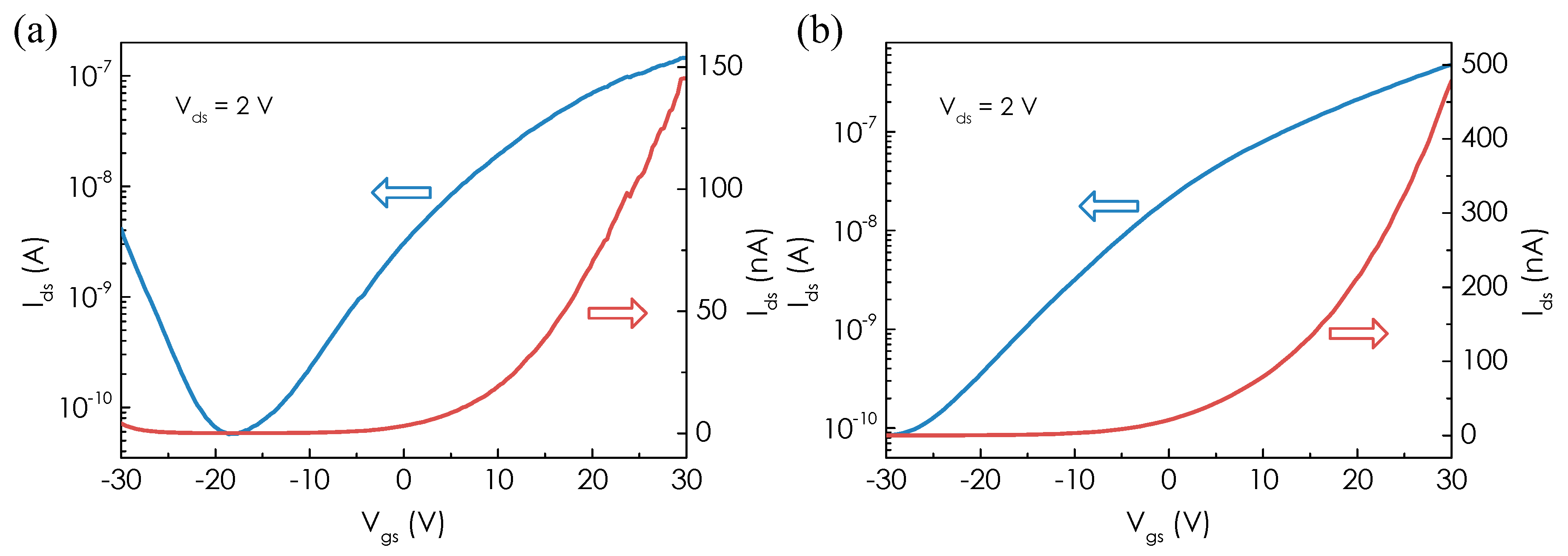
Figure 3.
(a) Real-time conductance change of the MoTe2 sensor upon exposure to different concentrations of NH3 in the dark and under light illumination. (b) Sensitivity enhancement of the MoTe2 sensor as a function of wavelength (photon energy) at different concentrations of NH3. (c) Response of the MoTe2 sensor as a function of NH3 concentration in the dark and under light illumination with different wavelength. The calculated slope of the linear fitting (indicated by dashed line) is 196% ppm−1 under 254 nm UV light illumination. (d) Enlarged part response of the MoTe2 sensor as a function of NH3 concentration in the dark in (c). The calculated slope is 2.1% ppm−1.
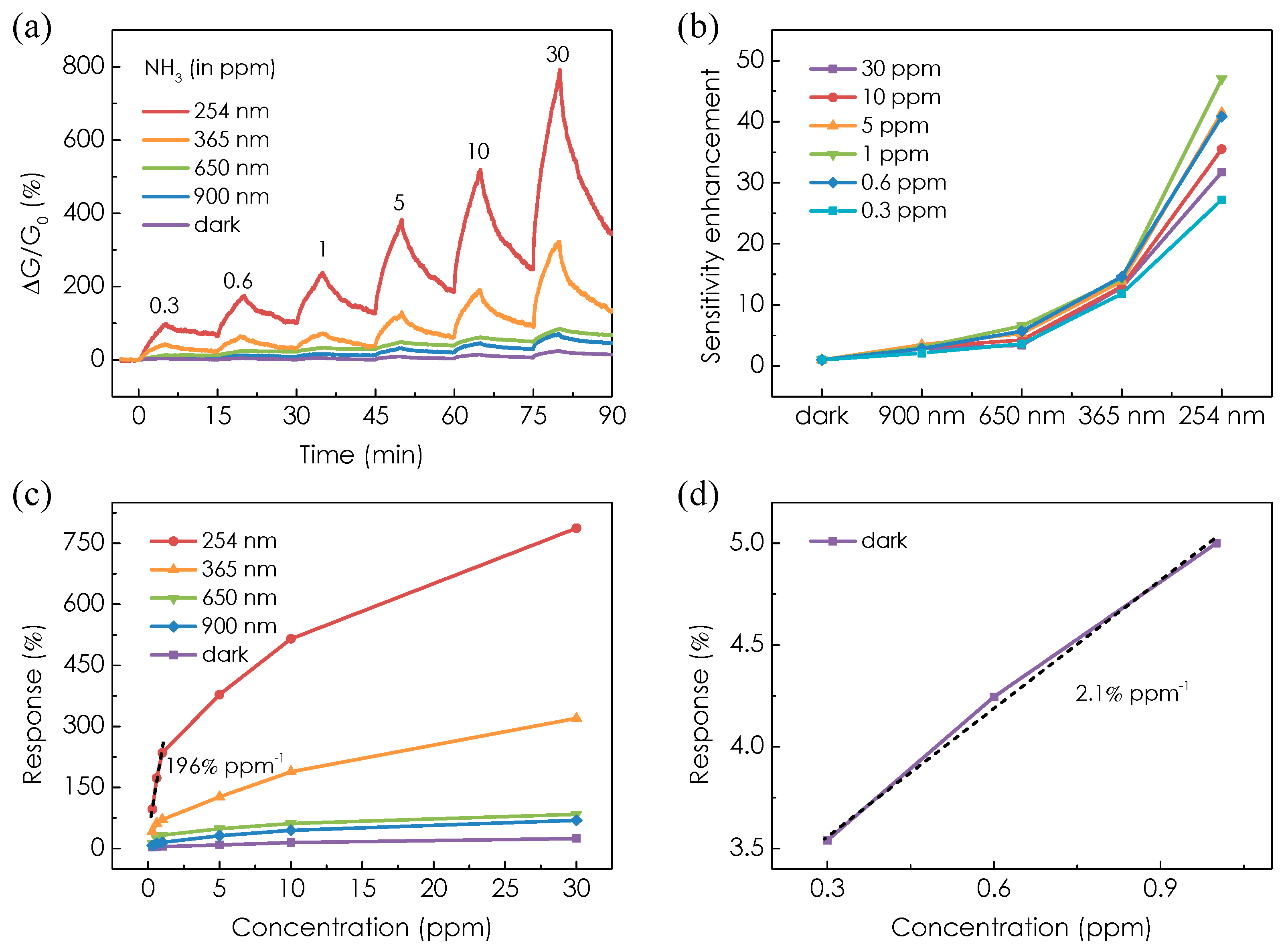
Figure 4.
(a) Real-time conductance change of the MoTe2 sensor upon exposure to different concentrations of NH3 under 254 nm UV light illumination with different intensity. (b) Response of the MoTe2 sensor as a function of light intensity at different concentrations of NH3. (c) Response of the MoTe2 sensor as a function of NH3 concentration under 254 nm UV light illumination with different intensity. The calculated slope of the linear fitting (indicated by dashed line) is 90.42% ppm−1 and 196% ppm−1 at intensity of 0.25 mW/cm2 and 2.5 mW/cm2, respectively.

© 2017 by the authors. Licensee MDPI, Basel, Switzerland. This article is an open access article distributed under the terms and conditions of the Creative Commons Attribution (CC BY) license (http://creativecommons.org/licenses/by/4.0/).
Share and Cite
MDPI and ACS Style
Feng, Z.; Xie, Y.; Wu, E.; Yu, Y.; Zheng, S.; Zhang, R.; Chen, X.; Sun, C.; Zhang, H.; Pang, W.; et al. Enhanced Sensitivity of MoTe2 Chemical Sensor through Light Illumination. Micromachines 2017, 8, 155. https://doi.org/10.3390/mi8050155
AMA Style
Feng Z, Xie Y, Wu E, Yu Y, Zheng S, Zhang R, Chen X, Sun C, Zhang H, Pang W, et al. Enhanced Sensitivity of MoTe2 Chemical Sensor through Light Illumination. Micromachines. 2017; 8(5):155. https://doi.org/10.3390/mi8050155
Chicago/Turabian StyleFeng, Zhihong, Yuan Xie, Enxiu Wu, Yuanyuan Yu, Shijun Zheng, Rui Zhang, Xuejiao Chen, Chonglin Sun, Hao Zhang, Wei Pang, and et al. 2017. "Enhanced Sensitivity of MoTe2 Chemical Sensor through Light Illumination" Micromachines 8, no. 5: 155. https://doi.org/10.3390/mi8050155
Note that from the first issue of 2016, this journal uses article numbers instead of page numbers. See further details here.