
Design and Fabrication of a 2-Axis Electrothermal MEMS Micro-Scanner for Optical Coherence Tomography †

 ,
, 
Abstract
:1. Introduction
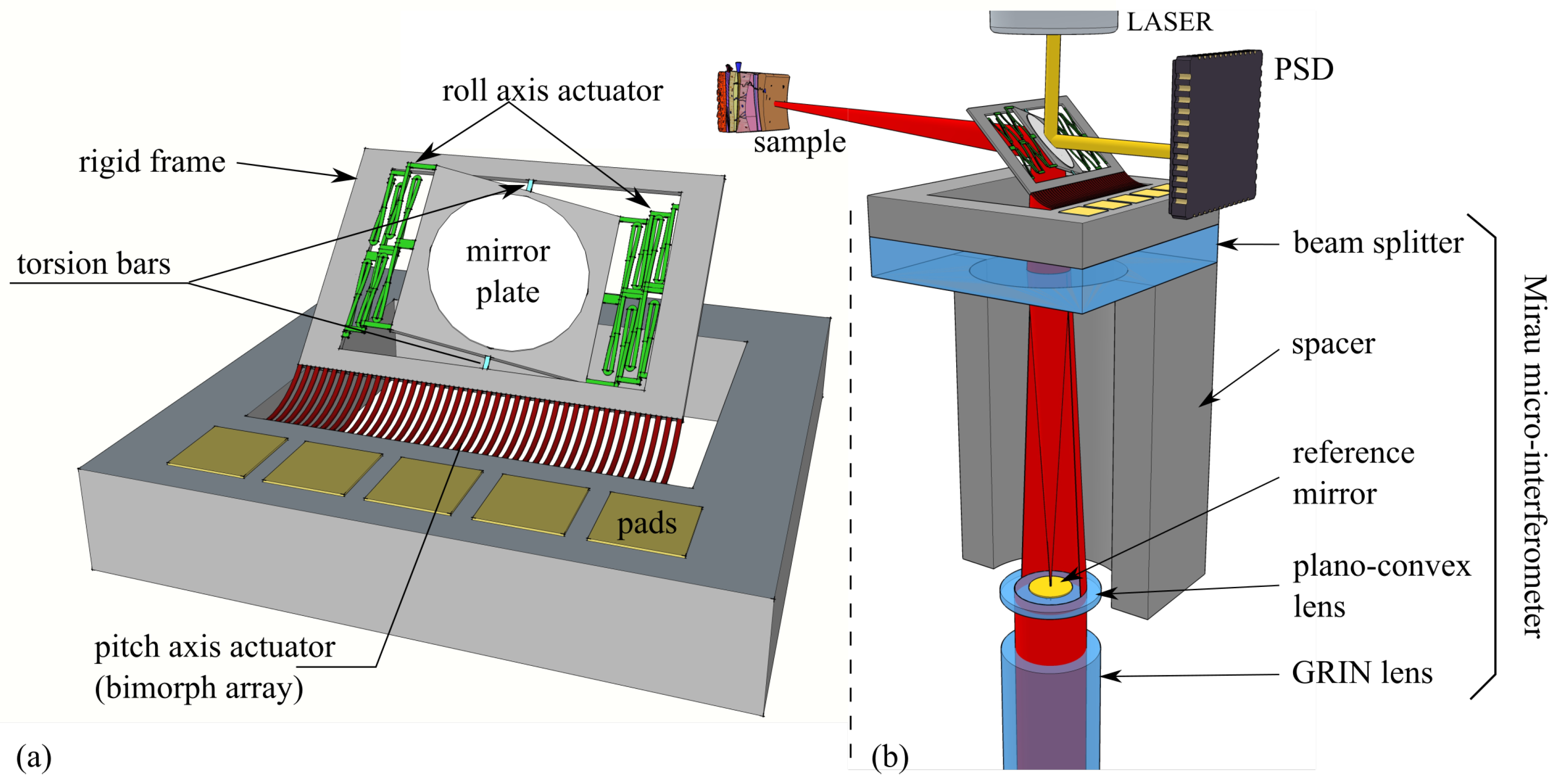
2. Design of the Device
2.1. Torsion Bar
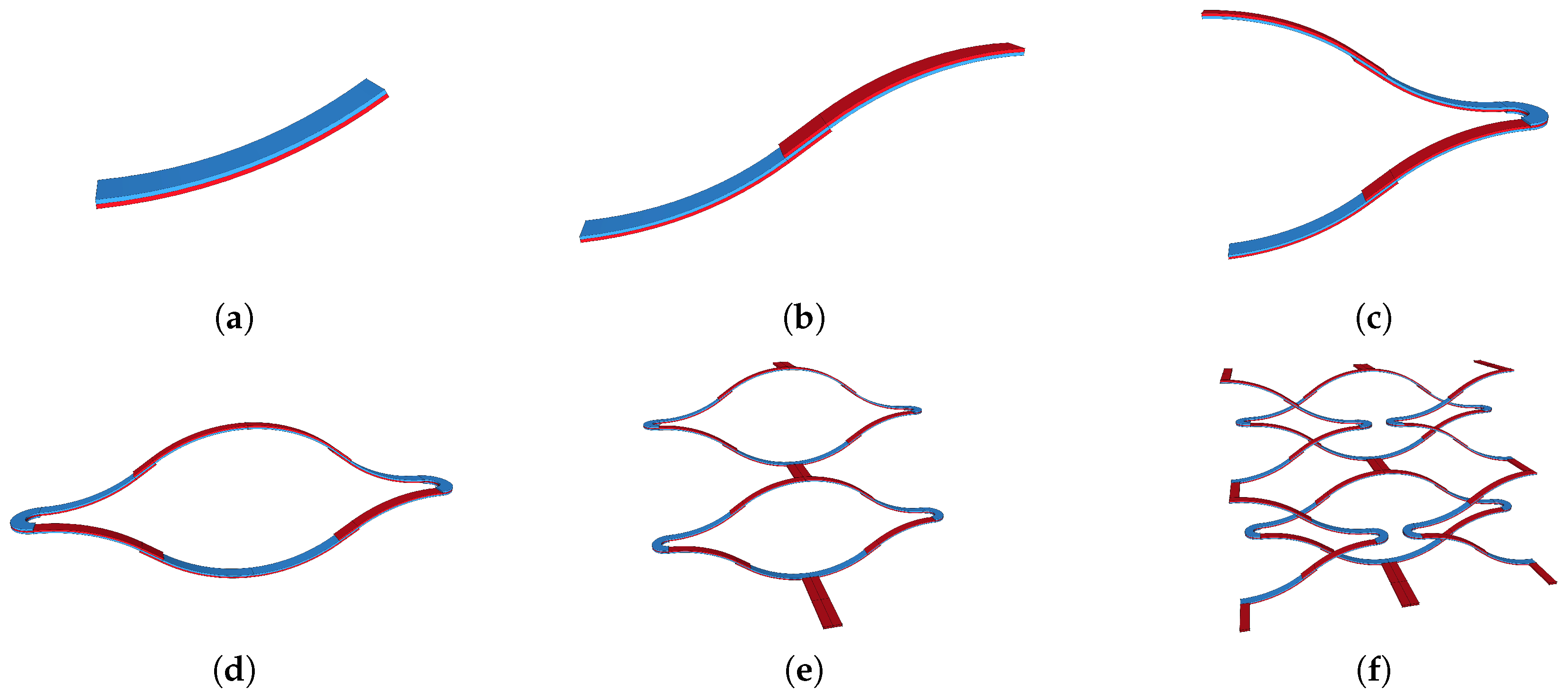
2.2. Electrothermal Actuation & MISC Actuators
2.3. Dual-Reflective Mirror Plate
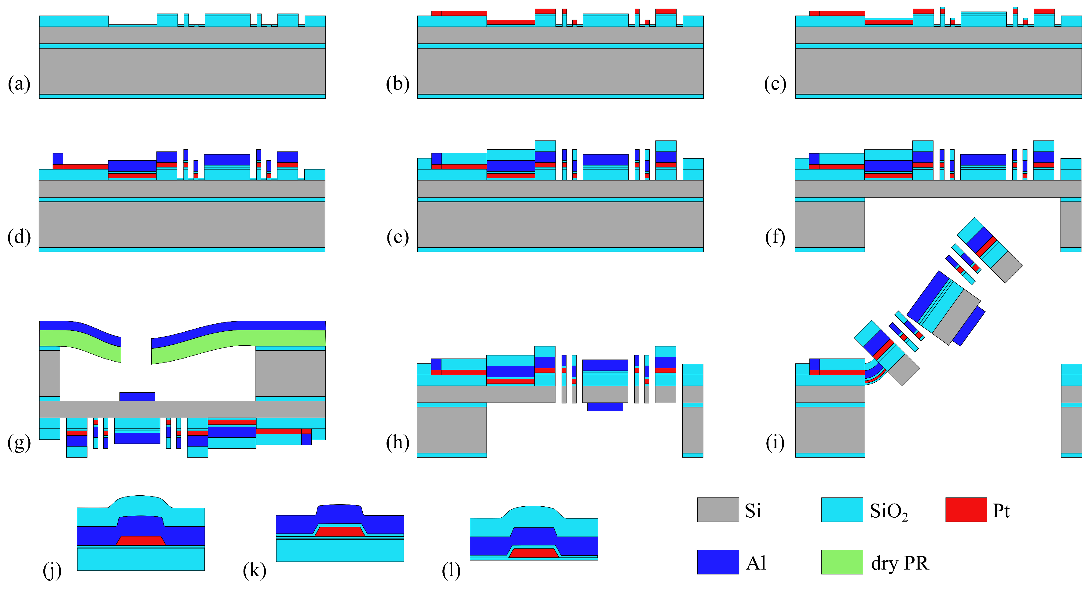
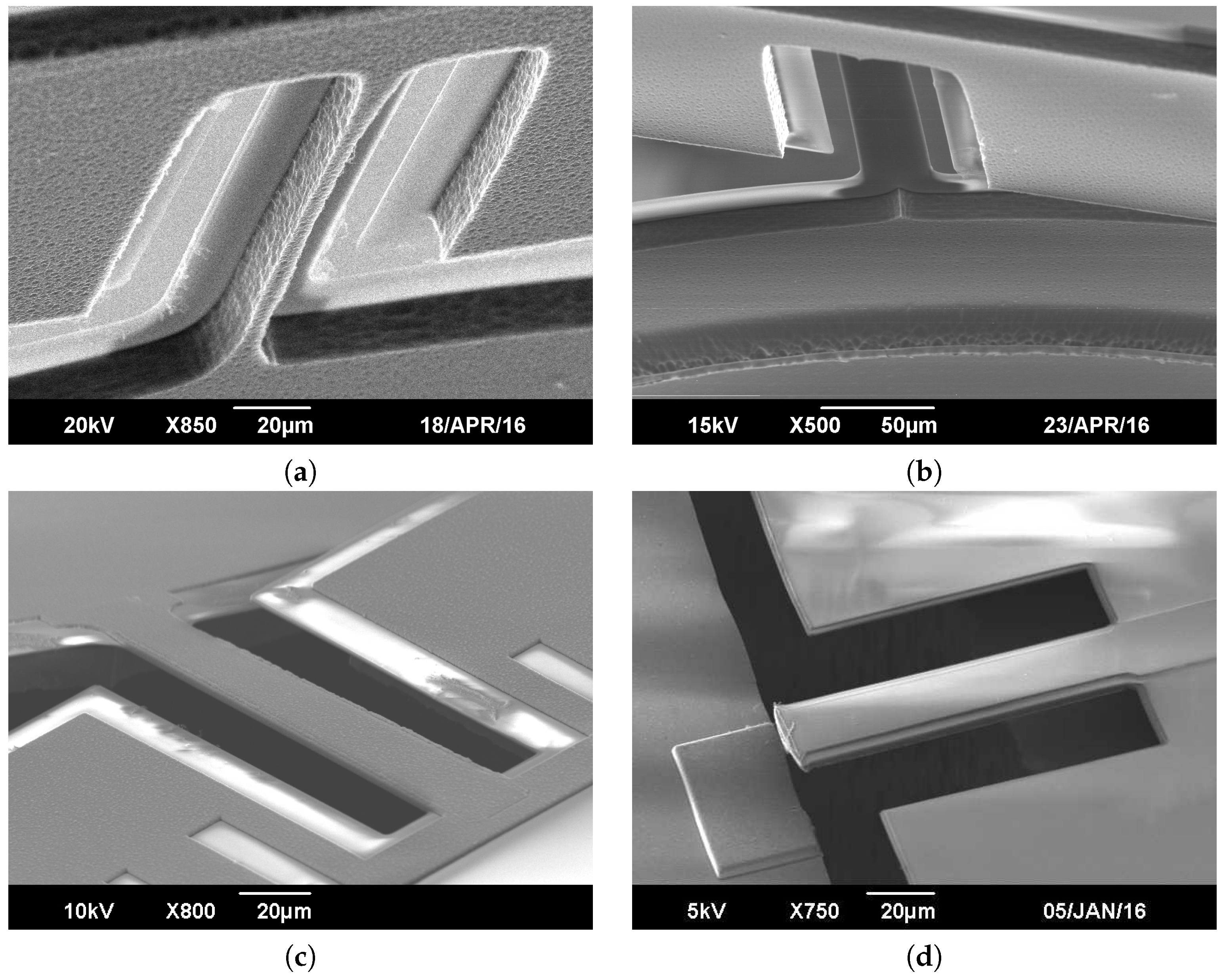
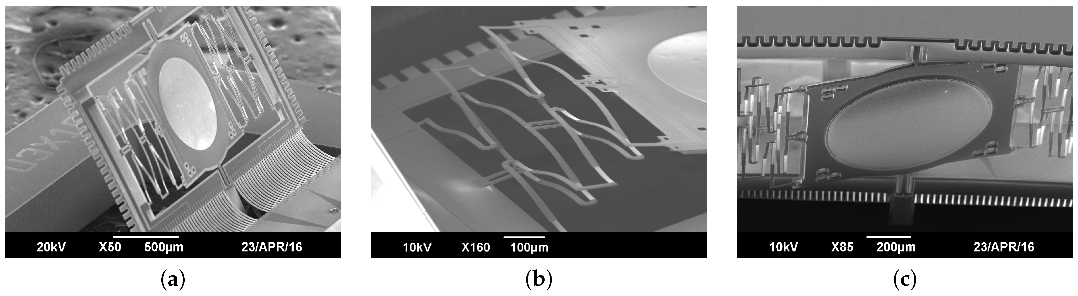
3. Fabrication
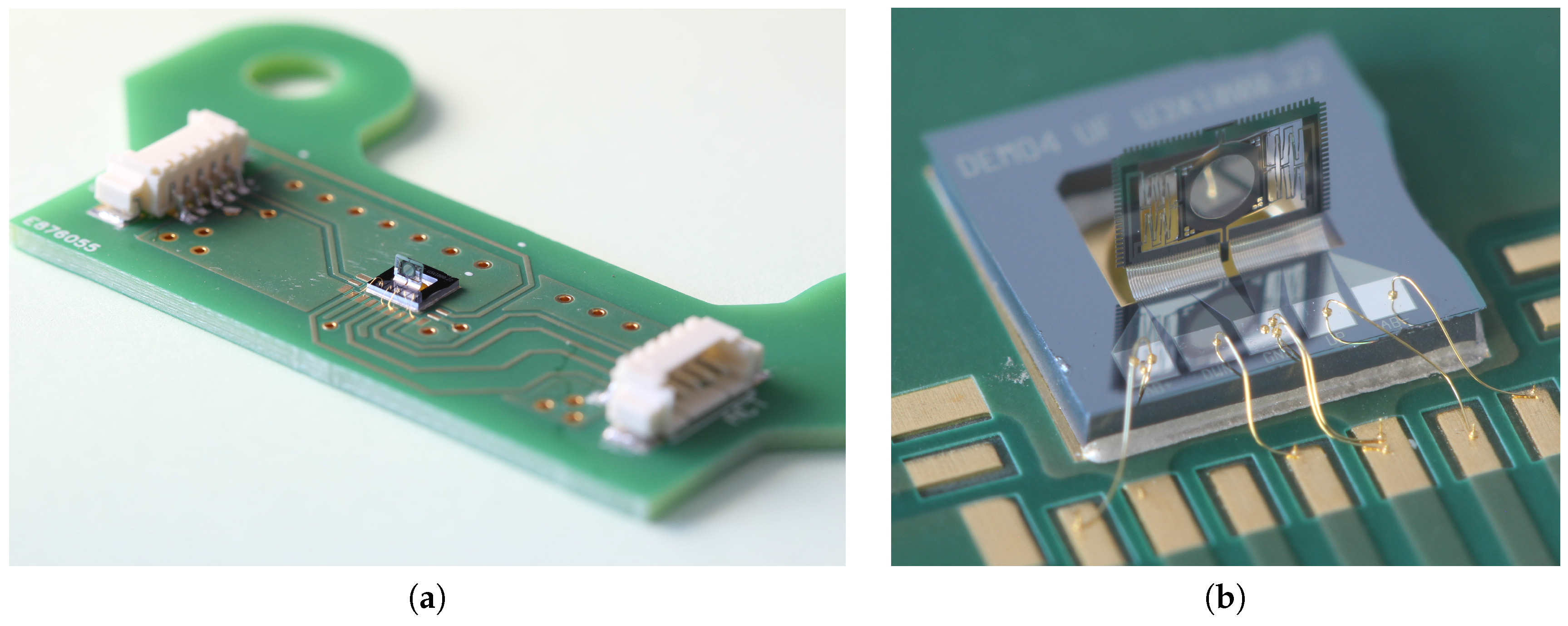
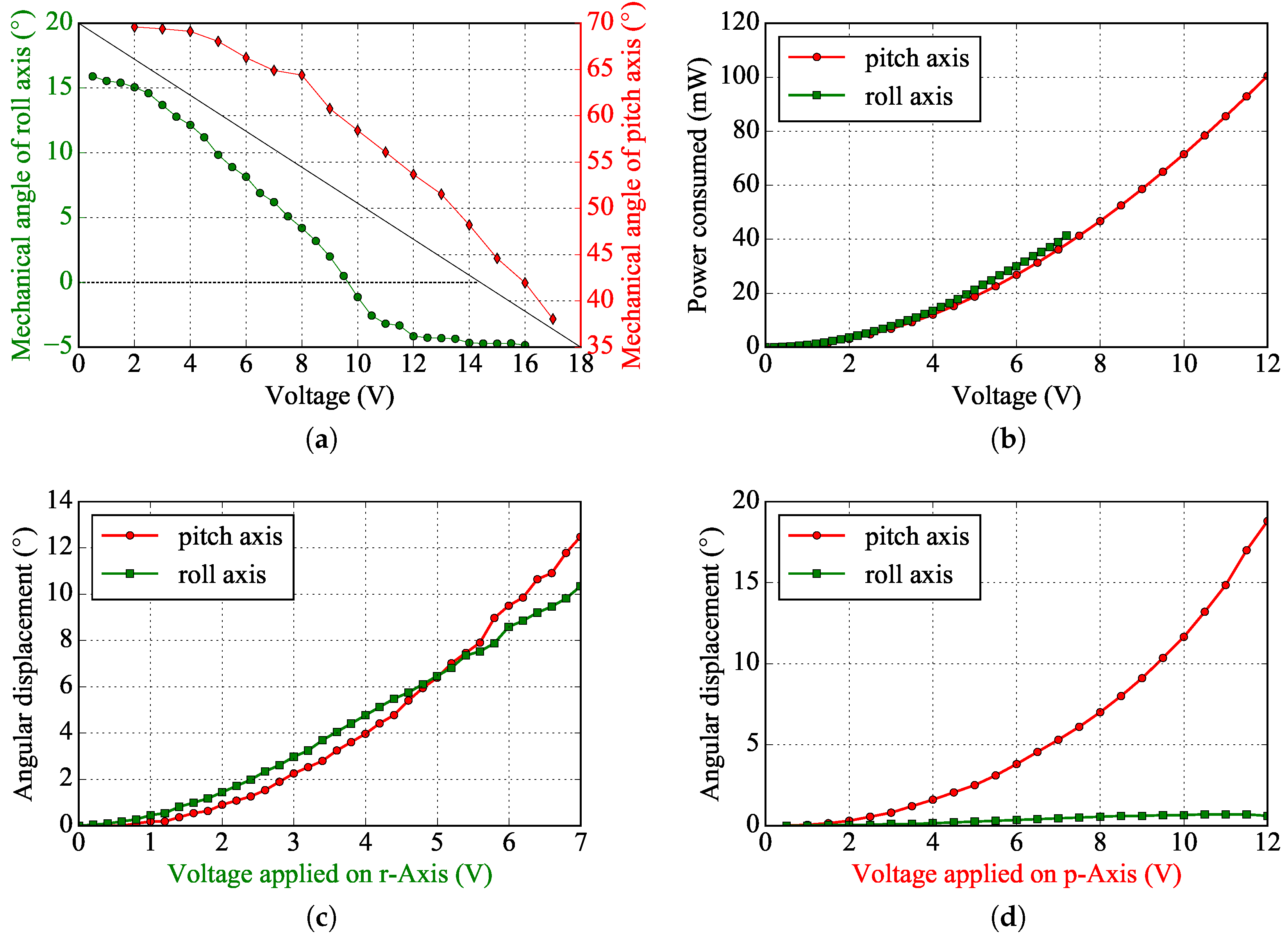
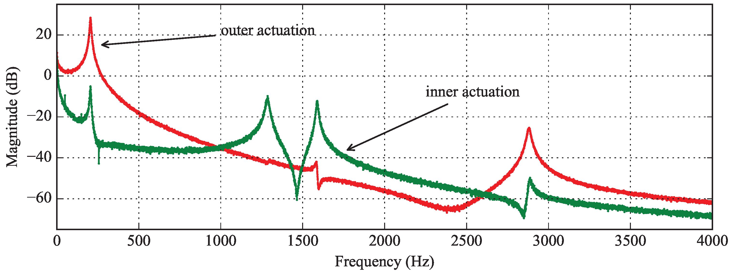
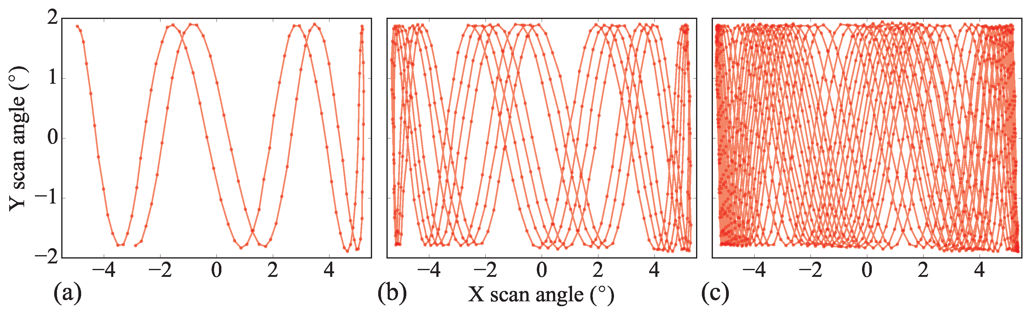
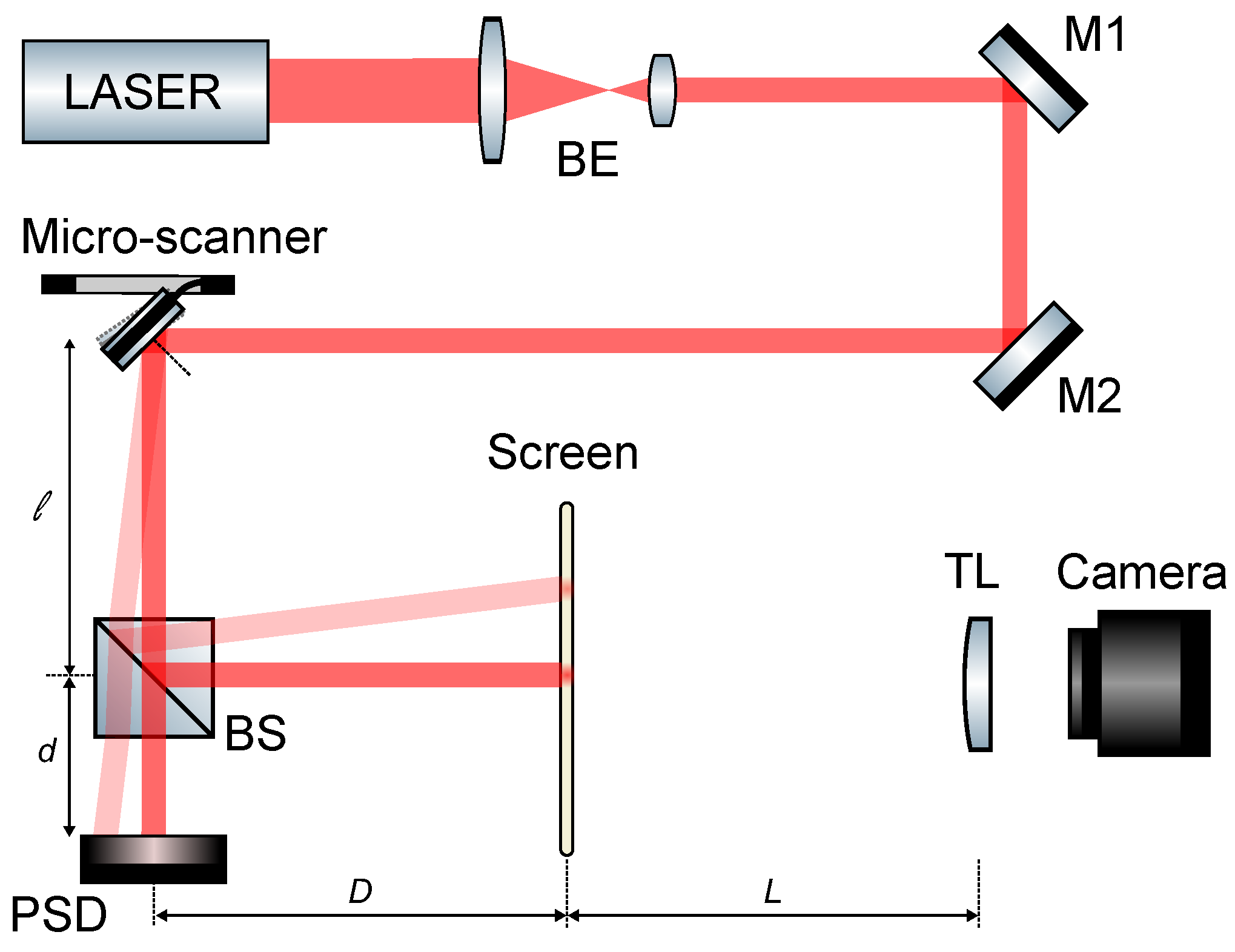
4. Characterization
Acknowledgments
Author Contributions
Conflicts of Interest
Abbreviations
| MEMS | Micro Electro-Mechanical System |
| MOEMS | Micro Optical Electro-Mechanical System |
| SCS | Single Crystal Silicon |
| OCT | Optical Coherence Tomography |
| SS | Swept Source |
| ISC | Inverted Series Connected |
| MISC | Meshed ISC |
| SOI | Silicon On Insulator |
| BOX | Buried Oxide |
| BOE | Buffered Oxide Etch |
| PECVD | Plasma-Enhanced Chemical Vapor Deposition |
| CTE | Coefficient of Thermal Expansion |
| RIE | Reactive-Ion Etching |
| ICP | Inductive Coupled Plasma |
| GRIN | GRadient INdex |
| PSD | Position Sensing Detector |
References
- Petersen, K.E. Silicon torsional scanning mirror. IBM J. Res. Dev. 1980, 24, 631–637. [Google Scholar] [CrossRef]
- Sun, J.; Xie, H. MEMS-based endoscopic optical coherence tomography. Int. J. Opt. 2011, 2011, 825629. [Google Scholar] [CrossRef]
- Sun, J.; Guo, S.; Wu, L.; Liu, L.; Choe, S.W.; Sorg, B.S.; Xie, H. 3D In Vivo optical coherence tomography based on a low-voltage, large-scan-range 2D MEMS mirror. Opt. Express 2010, 18, 12065–12075. [Google Scholar] [CrossRef] [PubMed]
- Struk, P.; Bargiel, S.; Froehly, L.; Baranski, M.; Passilly, N.; Albero, J.; Gorecki, C. Swept source optical coherence tomography endomicroscope based on vertically integrated mirau micro interferometer: Concept and technology. IEEE Sens. J. 2015, 15, 7061–7070. [Google Scholar] [CrossRef]
- Wu, L.; Xie, H. A large vertical displacement electrothermal bimorph microactuator with very small lateral shift. Sens. Actuators A Phys. 2008, 145–146, 371–379. [Google Scholar] [CrossRef]
- Todd, S.T.; Jain, A.; Qu, H.; Xie, H. A multi-degree-of-freedom micromirror utilizing inverted-series-connected bimorph actuators. J. Opt. A Pure Appl. Opt. 2006, 8, S352. [Google Scholar] [CrossRef]
- Jia, K.; Pal, S.; Xie, H. An electrothermal tip-tilt-piston micromirror based on folded dual S-shaped bimorphs. J. Microelectromech. Syst. 2009, 18, 1004–1015. [Google Scholar]
- Kobayashi, T.; Maeda, R. Piezoelectric optical micro scanner with built-in torsion sensors. Jpn. J. Appl. Phys. Part 1 Regul. Pap. Short Notes Rev. Pap. 2007, 46, 2781–2784. [Google Scholar] [CrossRef]
- Wang, W.; Chen, J.; Zivkovic, A.S.; Tanguy, Q.A.; Xie, H. A compact Fourier transform spectrometer on a silicon optical bench with an electrothermal MEMS mirror. J. Microelectromech. Syst. 2016, 25, 347–355. [Google Scholar] [CrossRef]
- Han, F.; Wang, W.; Zhang, X.; Xie, H. Modeling and control of a large-stroke electrothermal MEMS mirror for fourier transform microspectrometers. J. Microelectromech. Syst. 2016, 25, 750–760. [Google Scholar] [CrossRef]
- Wang, W.; Chen, J.; Zivkovic, A.S.; Xie, H. A Fourier Transform Spectrometer based on an electrothermal MEMS mirror with improved linear scan range. Sensors 2016, 16, 1611. [Google Scholar] [CrossRef] [PubMed]
- Zhao, Y.; Tay, F.E.H.; Zhou, G.; Chau, F.S. Fast and precise positioning of electrostatically actuated dual-axis micromirror by multi-loop digital control. Sens. Actuators A Phys. 2006, 132, 421–428. [Google Scholar] [CrossRef]
- Fujita, T.; Maenaka, K.; Takayama, Y. Dual-axis MEMS mirror for large deflection-angle using SU-8 soft torsion beam. Sens. Actuators A Phys. 2005, 121, 16–21. [Google Scholar] [CrossRef]
- Tseng, V.F.G.; Xie, H. Simultaneous piston position and tilt angle sensing for large vertical displacement micromirrors by frequency detection inductive sensing. Appl. Phys. Lett. 2015, 107, 214102. [Google Scholar] [CrossRef]
- Lowet, G.; Audekercke, R.V.; der Perre, G.V.; Geusens, P.; Dequeker, J.; Lammens, J. The relation between resonant frequencies and torsional stiffness of long bones in vitro. Validation of a simple beam model. J. Biomech. 1993, 26, 689–696. [Google Scholar] [CrossRef]
- Timoshenko, S. Analysis of Bi-metal thermostats. J. Opt. Soc. Am. 1925, 11, 233–255. [Google Scholar] [CrossRef]
- Ji, C.H.; Kim, Y.K. Electromagnetic micromirror array with single-crystal silicon mirror plate and aluminum spring. J. Lightw. Technol. 2003, 21, 584–590. [Google Scholar]
- Young, W.; Roark, R.; Budynas, R. Roark’s Formulas for Stress and Strain; McGraw-Hill: New York, NY, USA, 2002; Volume 7. [Google Scholar]
- Liu, L.; Pal, S.; Xie, H. MEMS mirrors based on a curved concentric electrothermal actuator. Sens. Actuators A Phys. 2012, 188, 349–358. [Google Scholar] [CrossRef]
- Todd, S.T.; Xie, H. Steady-state 1D electrothermal modeling of an electrothermal transducer. J. Micromech. Microeng. 2006, 16, 665. [Google Scholar] [CrossRef]
- Jain, A.; Kopa, A.; Pan, Y.; Feeder, G.K.; Xie, H. A two-axis electrothermal micromirror for endoscopic optical coherence tomography. IEEE J. Sel. Top. Quantum Electron. 2004, 10, 636–642. [Google Scholar] [CrossRef]
- Samuelson, S.R.; Xie, H. A large piston displacement MEMS mirror with electrothermal ladder actuator arrays for ultra-low tilt applications. J. Microelectromech. Syst. 2014, 23, 39–49. [Google Scholar] [CrossRef]


© 2017 by the authors. Licensee MDPI, Basel, Switzerland. This article is an open access article distributed under the terms and conditions of the Creative Commons Attribution (CC BY) license (http://creativecommons.org/licenses/by/4.0/).
Share and Cite
Tanguy, Q.A.A.; Bargiel, S.; Xie, H.; Passilly, N.; Barthès, M.; Gaiffe, O.; Rutkowski, J.; Lutz, P.; Gorecki, C. Design and Fabrication of a 2-Axis Electrothermal MEMS Micro-Scanner for Optical Coherence Tomography. Micromachines 2017, 8, 146. https://doi.org/10.3390/mi8050146
Tanguy QAA, Bargiel S, Xie H, Passilly N, Barthès M, Gaiffe O, Rutkowski J, Lutz P, Gorecki C. Design and Fabrication of a 2-Axis Electrothermal MEMS Micro-Scanner for Optical Coherence Tomography. Micromachines. 2017; 8(5):146. https://doi.org/10.3390/mi8050146
Chicago/Turabian StyleTanguy, Quentin A. A., Sylwester Bargiel, Huikai Xie, Nicolas Passilly, Magali Barthès, Olivier Gaiffe, Jaroslaw Rutkowski, Philippe Lutz, and Christophe Gorecki. 2017. "Design and Fabrication of a 2-Axis Electrothermal MEMS Micro-Scanner for Optical Coherence Tomography" Micromachines 8, no. 5: 146. https://doi.org/10.3390/mi8050146