Controlled Solvent-Free Formation of Embedded PDMS-Derived Carbon Nanodomains with Tunable Fluorescence Using Selective Laser Ablation with A Low-Power CD Laser


Abstract
:1. Introduction
2. Materials and Methods
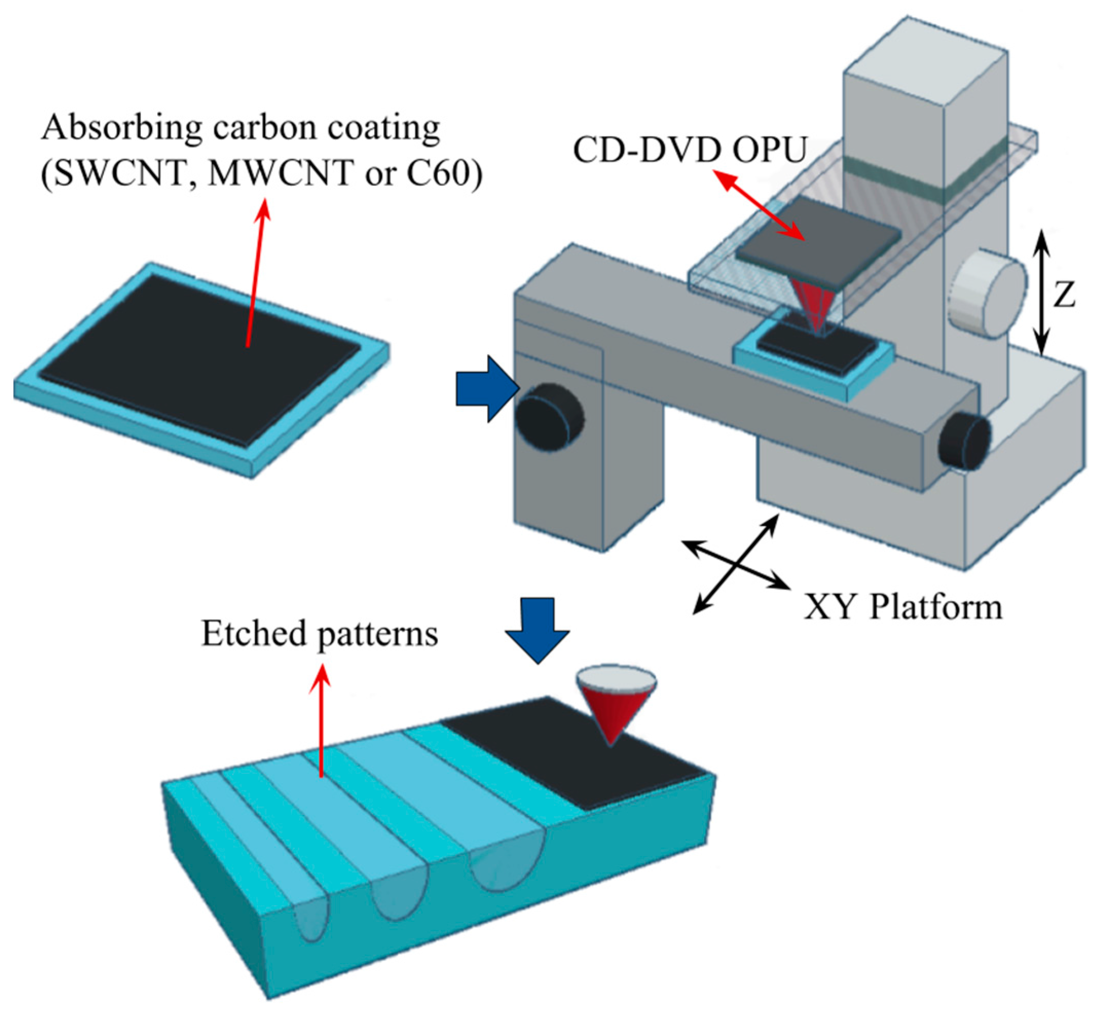
2.1. Samples Preparation
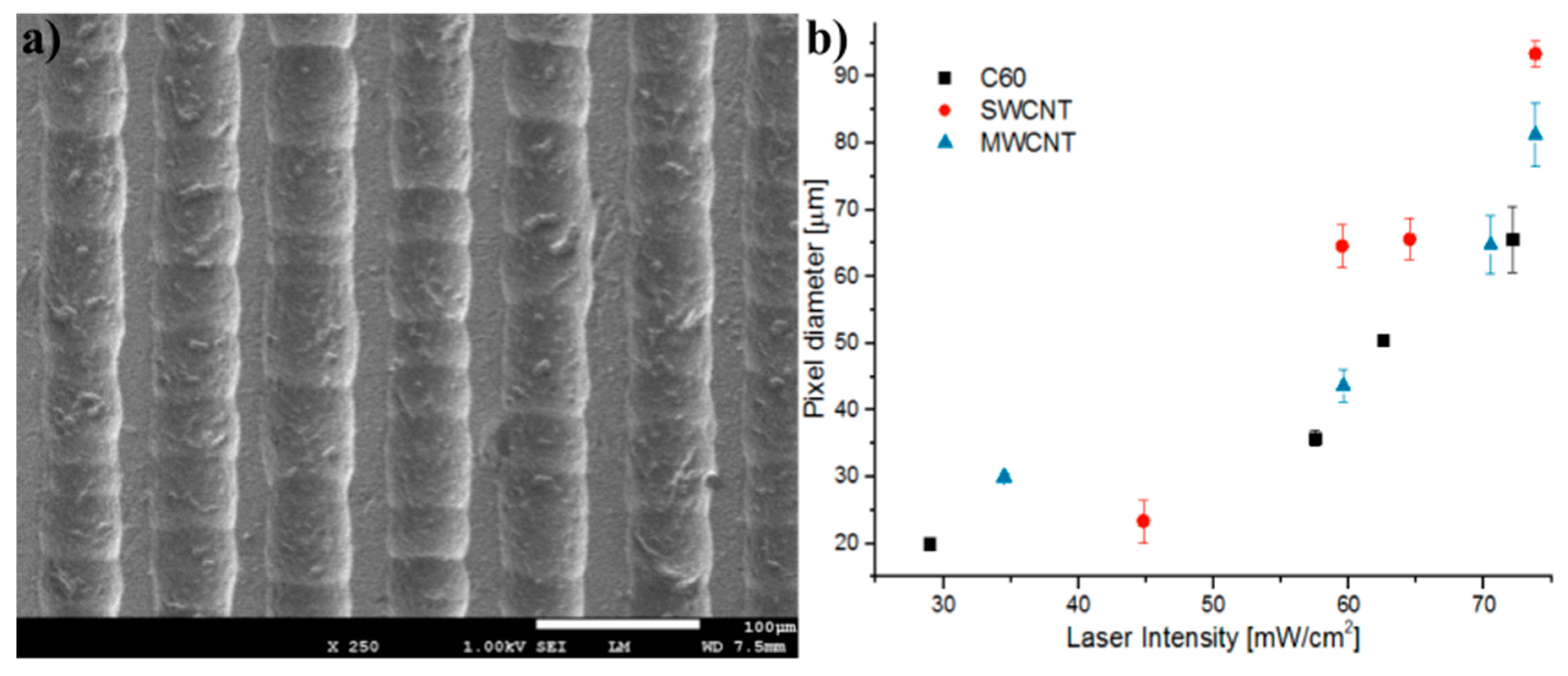
2.2. Laser Etching of Micropatterns
2.3. Characterisation of Nanocarbon Residues and Tunable Fluorescence
3. Results
3.1. Etching Process Results
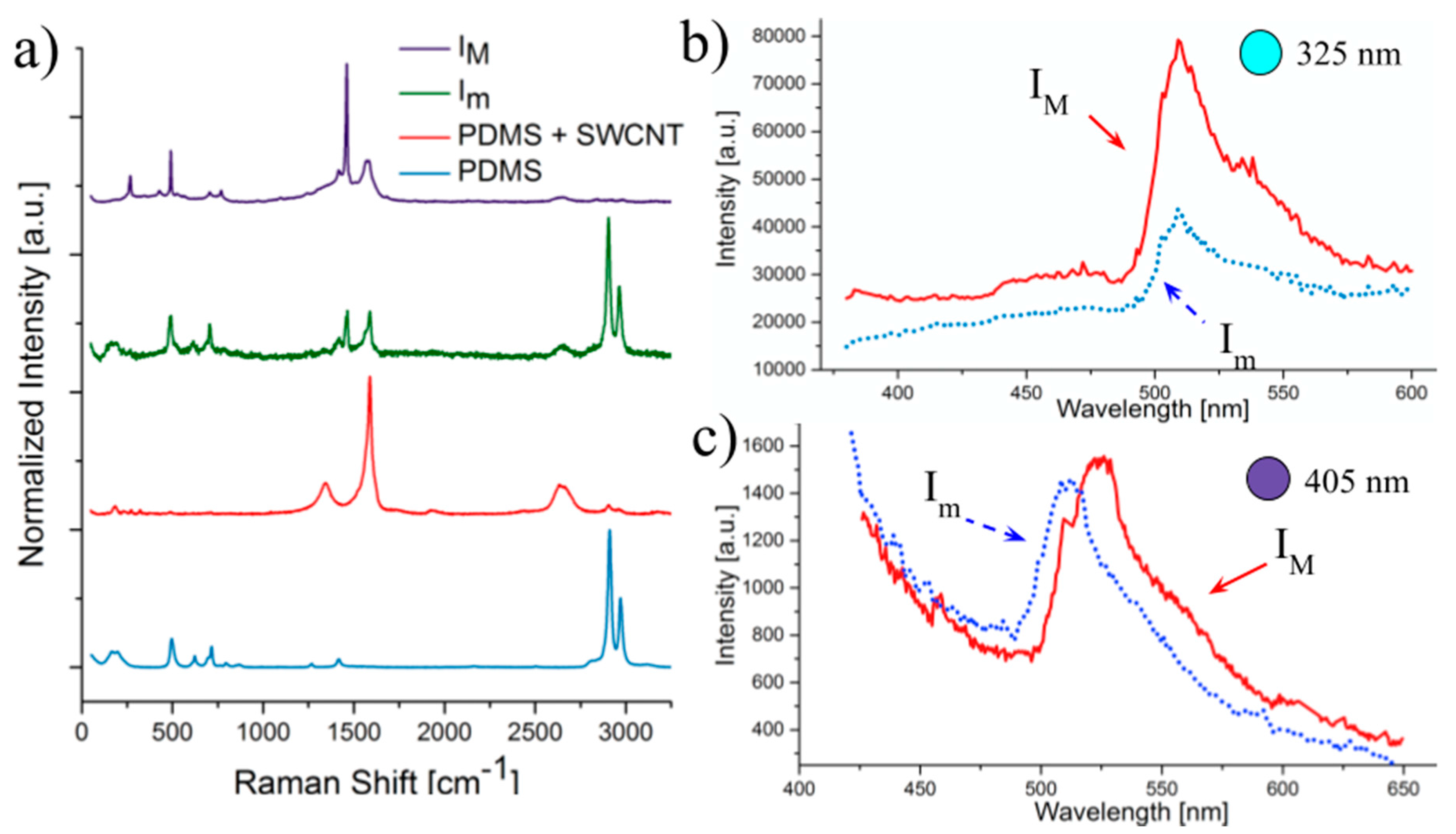
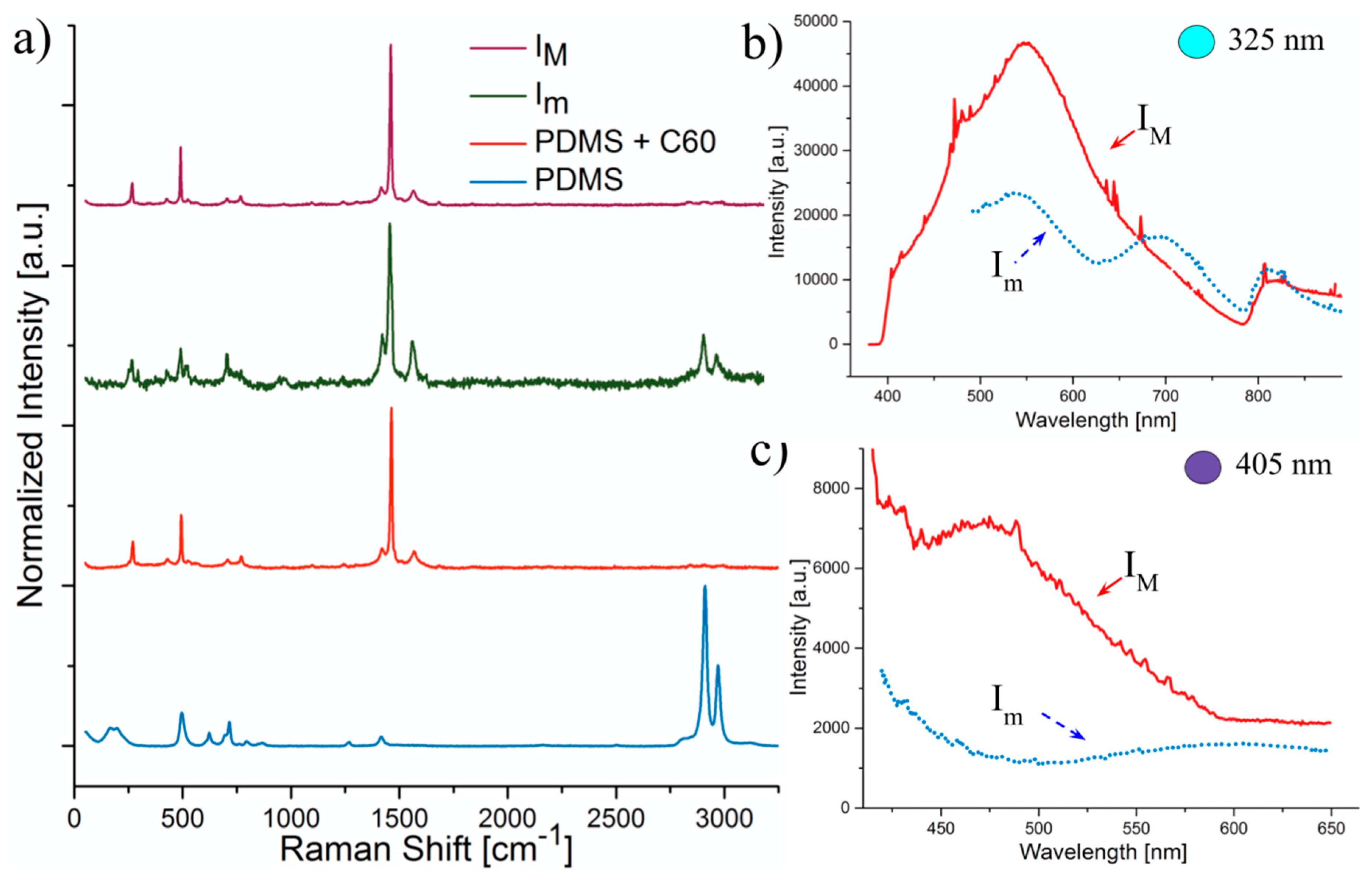
3.2. Spectroscopy Results
3.2.1. SWCNT
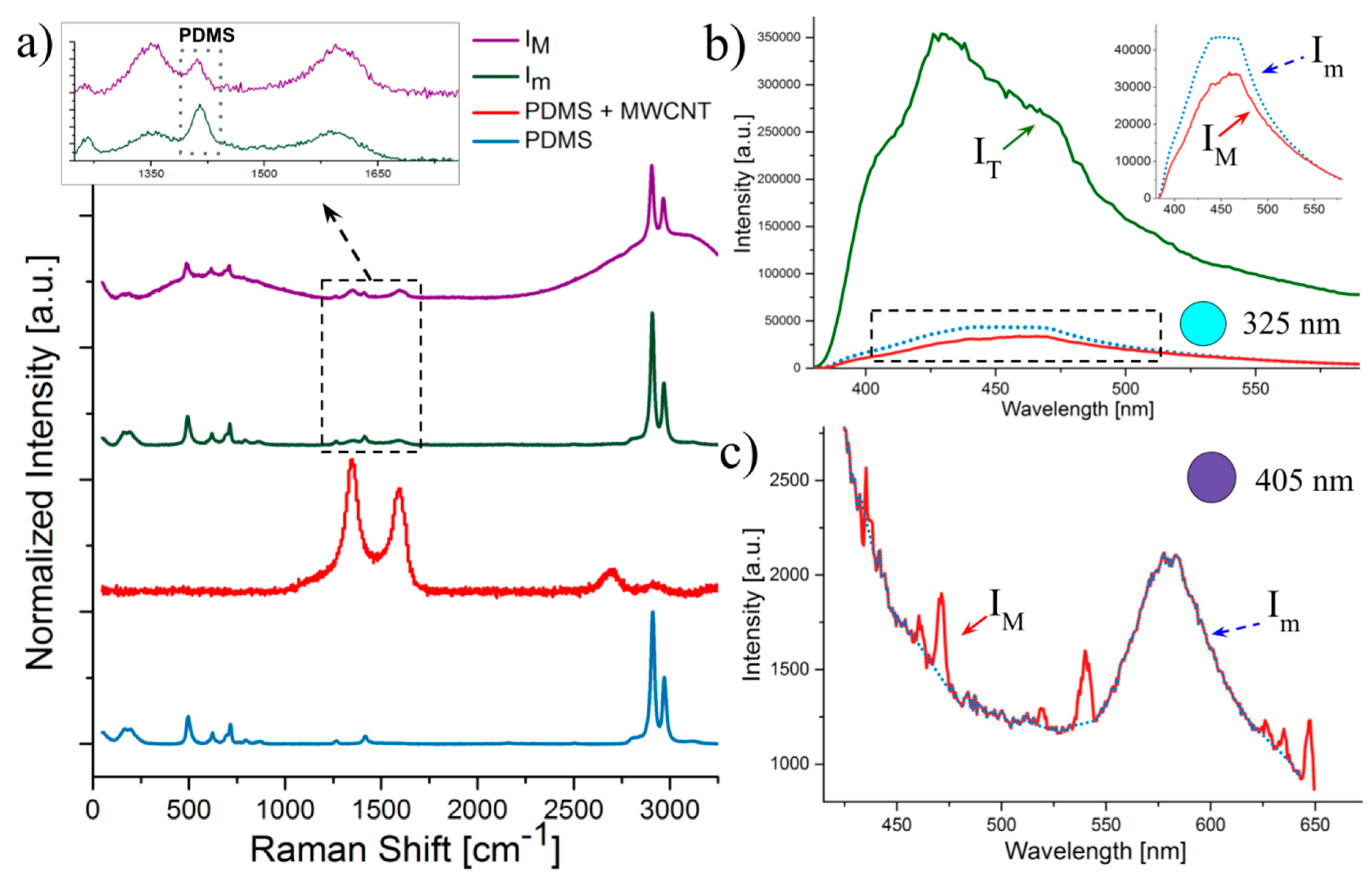
3.2.2. MWCNT
3.2.3. C60
4. Conclusions
Acknowledgments
Author Contributions
Conflicts of Interest
References
- Baudach, S.; Bonse, J.; Krüger, J.; Kautek, W. Ultrashort Pulse Laser Ablation of Polycarbonate and Polymethylmethacrylate. Appl. Surf. Sci. 2000, 154, 555–560. [Google Scholar] [CrossRef]
- Kallepalli, L.N.D.; Soma, V.R.; Desai, N.R. Femtosecond-Laser Direct Writing in Polymers and Potential Applications in Microfluidics and Memory Devices. Opt. Eng. 2012, 51, 073402. [Google Scholar] [CrossRef]
- Gattas, R.R.; Mazur, E. Femtosecond Laser Micromachining in Transparent Materials. Nat. Photon. 2008, 2, 219–225. [Google Scholar] [CrossRef]
- Liu, X.; Du, D.; Mourou, G. Laser Ablation and Micromachining with Ultrashort Laser Pulses. IEEE J. Quantum Electron. 1997, 33, 1706–1716. [Google Scholar] [CrossRef]
- Tsouti, V.; Boutopoulos, C.; Goustouridis, D.; Zergioti, L.; Normand, P.; Tsoukalas, D.; Chatzandroulis, S. A Chemical Sensor Microarray Realized by Laser Printing of Polymers. Sens. Actuators B Chem. 2010, 150, 148–153. [Google Scholar] [CrossRef]
- Chong, T.C.; Hong, M.H.; Shi, L.P. Laser Precision Engineering: From Microfabrication to Nanoprocessing. Laser Photon. Rev. 2010, 4, 123–143. [Google Scholar] [CrossRef]
- McDonald, J.C.; Whitesides, G.M. Poly(dimethylsiloxane) as a Material for Fabricating Microfluidic Devices. Acc. Chem. Res. 2002, 35, 491–499. [Google Scholar] [CrossRef] [PubMed]
- Menard, E.; Meitl, M.A.; Sun, Y.; Park, J.U.; Shir, D.J.L.; Nam, Y.S.; Jeon, S.; Rogers, J.A. Micro and Nanopatterning Techniques for Organic Electronic and Optoelectronic Systems. Chem. Rev. 2007, 107, 1117–1160. [Google Scholar] [CrossRef] [PubMed]
- Chang-Yen, D.A.; Eich, R.K.; Gale, B.K. A Monolithic PDMS Waveguide System Fabricated Using Soft-Litography Techniques. J. Lightwave Technol. 2005, 23, 2088–2093. [Google Scholar] [CrossRef]
- Alshehri, A.M.; Deepak, K.L.N.; Marquez, D.T.; Desgreniers, S.; Bhardwaj, V.R. Localized Nanoclusters Formation in PDMS upon Irradiation with Femtosecond Laser. Opt. Mater. Express. 2015, 5, 858–869. [Google Scholar] [CrossRef]
- Unal, A.A.; Stalmashonak, A.; Seifert, G.; Graener, H. Ultrafast Dynamics of Silver Nanoparticle Shape Transformation Studied by Femtosecond Pulse-Pair Irradiation. Phys. Rev. B 2009, 79, 115411. [Google Scholar] [CrossRef]
- Stalmashonak, A.; Graener, H.; Seifert, G. Transformation of Silver Nanospheres Embedded in Glass to Nanodisks Using Circularly Polarized Femtosecond Pulses. Appl. Phys. Lett. 2009, 94, 193111. [Google Scholar] [CrossRef]
- Li, X.; Wang, H.; Shimizu, Y.; Pyatenko, A.; Kawaguchi, K.; Koshizaki, N. Preparation of Carbon Quantum Dots with Tunable Photoluminescence by Rapid Laser Passivation in Ordinary Organic Solvents. Chem. Commun. 2011, 47, 932–934. [Google Scholar] [CrossRef] [PubMed]
- Hu, S.L.; Niu, K.Y.; Sun, J.; Yang, J.; Zhao, N.Q.; Du, X.W. One-step Synthesis of Fluorescent Carbon Nanoparticles by Laser Irradiation. J. Mater. Chem. 2009, 19, 484–488. [Google Scholar] [CrossRef]
- Hautefeuille, M.; Jimenez-Zenteno, A.K.; Pérez-Alcázar, P.R.; Hess-Frieling, K.M.; Fernandez-Sanchez, G.; Velazquez, V.; Grether-Gonzalez, M.; Lopez-Moreno, E. Utilization of a Digital-Versatile-Disc Pickup Head for Benchtop Laser Microfabrication. Appl. Opt. 2012, 51, 1171–1177. [Google Scholar] [CrossRef] [PubMed]
- Hautefeuille, M.; Cabriales, L.; Pimentel-Domínguez, R.; Velázquez, V.; Hernández-Cordero, J.; Oropeza-Ramos, L.; Rivera, M.; Carreón-Castro, M.P.; Grether, M.; López-Moreno, E. New Perspectives for Direct PDMS Microfabrication Using a CD-DVD Laser. Lab Chip 2013, 13, 4848–4854. [Google Scholar] [CrossRef] [PubMed]
- Alcántara, J.C.; Zorrilla, M.; Cabriales, L.; León, L.M.; Hautefeuille, M. Low Cost Formation of Bulk and Localized Polymer-Derived Carbon Nanodomains from Polydimethylsiloxane. Beilstein J. Nanotechnol. 2015, 6, 744–748. [Google Scholar] [CrossRef] [PubMed]
- Vivien, L.; Lançon, P.; Riehl, D.; Hache, F.; Anglaret, E. Carbon Nanotubes for Optical Limiting. Carbon 2002, 40, 1789–1797. [Google Scholar] [CrossRef]
- Kempa, K. Gapless Plasmons in Carbon Nanotubes and their Interactions with Phonons. Phys. Rev. B 2002, 66, 195406. [Google Scholar] [CrossRef]
- Lim, K.Y.; Sow, C.H.; Lin, J.; Cheong, F.C.; Shen, Z.X.; Thong, J.T.L.; Chin, K.C.; Wee, A.T.S. Laser Pruning of Carbon Nanotubes as a Route to Static and Movable Structures. Adv. Mater. 2003, 15, 300–303. [Google Scholar] [CrossRef]
- Cheong, F.C.; Lim, K.Y.; Sow, C.H.; Lin, J.; Ong, C.K. Large Area Patterned Arrays of Aligned Carbon Nanotubes Via Laser Trimming. Nanotechonolgy 2003, 14, 433–437. [Google Scholar] [CrossRef]
- Pimentel-Domínguez, R.; Velázquez-Benítez, A.M.; Vélez-Cordero, J.R.; Hautefeuille, M.; Sánchez-Arévalo, F.; Hernández-Cordero, J. Photothermal Effects and Applications of Polydimethylsiloxane Membranes with Carbon Nanoparticles. Polymers 2016, 8, 84. [Google Scholar] [CrossRef]
- Zillohu, A.U.; Abdelaziz, R.; Hedayati, M.K.; Emmler, T.; Homaeigohar, S.; Elbahri, M. Plasmon-Mediated Embedding of Nanoparticles in a Polymer Matrix: Nanocomposites Patterning, Writing, and Defect Healing. J. Phys. Chem. C 2012, 116, 17204–17209. [Google Scholar] [CrossRef]
- Santana, G.; Mejía, A.; Monroy, M.; López, M.; Casallas, Y.; Ramírez, M.; Contreras, G.; Melo, O. Photoluminescence Spectroscopy as a Tool for Quality Control of GaN Thin Film to be Used in Solar Cell Devices. Mater. Sci. Appl. 2014, 5, 267–270. [Google Scholar]
- Bahrami, A.A. Carbon Nanotubes as Near Infrared Laser Susceptors. Ph.D. thesis, University of Cambridge, Cambridge, UK, 2011. [Google Scholar]
- Lim, Z.H.; Lee, A.; Zhu, Y.; Lim, K.Y.; Sow, C.H. Sustained Laser Induced Incandescence in Carbon Nanotubes for Rapid Localized Heating. Appl. Phys. Lett. 2009, 94, 073106. [Google Scholar] [CrossRef]
- Genovese, A.; Shanks, R.A. Fire performance of Poly(dimethyl siloxane) Composites Evaluated by Cone Calorimetry. Compos. Part A 2008, 39, 398–405. [Google Scholar] [CrossRef]
- Camino, G.; Lomakin, S.M.; Lageard, M. Thermal Polydimethylsiloxane Degradation. Part 2. The Degradation Mechanisms. Polymer 2002, 43, 2011–2015. [Google Scholar]
- Ferrari, A.C.; Robertson, J. Interpretation of Raman Spectra of Disordered and Amorphous Carbon. Phys. Rev. B 2000, 61, 14095–14107. [Google Scholar] [CrossRef]
- Gauthier, M.A.; Stangel, I.; Ellis, T.H.; Zhu, X.X. A New Method for Quantifying the Intensity of the C=C Band of Dimethacrylate Dental Monomers in their FTIR and Raman Spectra. Biomaterials 2005, 26, 6440–6448. [Google Scholar] [CrossRef] [PubMed]
- Bae, S.C.; Lee, H.; Lin, Z.; Granick, S. Chemical Imaging in a Surface Forces Apparatus: Confocal Raman Spectroscopy of Confined Poly(dimethylsiloxane). Langmuir 2005, 21, 5685–5688. [Google Scholar] [CrossRef] [PubMed]
- Cai, D.; Neyer, A.; Kuckuk, R.; Heise, H.M. Raman, Mid-Infrared, Near-Infrared and Ultraviolet-Visible Spectroscopy of PDMS Silicone Rubber for Characterization of Polymer Optical Waveguide Materials. J. Mol. Struct. 2010, 976, 274–281. [Google Scholar] [CrossRef]
- Dupas-Bruzek, C.; Robbe, O.; Addad, A.; Turrell, S.; Derozier, D. Transformation of Medical Grade Silicone Rubber Under Nd:YAG and Excimer Laser Irradiation: First Step Towards a New Miniaturized Nerve Electrode Fabrication Process. Appl. Surf. Sci. 2009, 255, 8715–8721. [Google Scholar] [CrossRef]
- Baker, S.N.; Baker, G.A. Luminiscent Carbon Nanodots: Emergent Nanolights. Angew. Chem. Int. Ed. 2010, 49, 6726–6744. [Google Scholar] [CrossRef] [PubMed]
- Mittal, J.; Kushwaha, N. Over-oxidation of multi-walled carbon nanotubes and formation of fluorescent carbon nanoparticles. Mater. Lett. 2015, 145, 37–40. [Google Scholar] [CrossRef]
- Makarova, T.L. Electrical and Optical Properties of Pristine and Polymerized Fullerenes. Semiconductors 2001, 35, 243–278. [Google Scholar] [CrossRef]
- Venkateswaran, U.D.; Sanzi, D.; Rao, A.M.; Eklund, P.C.; Marques, L.; Hodeau, J.L.; Nunez-Regueiro, M. Temperature Dependence of the Photoluminescence in Polymeric Solid C60. Phys. Rev. B 1998, 57, R3193. [Google Scholar] [CrossRef]
- Kuzmany, H.; Pfeiffer, R.; Hulman, M.; Kramberger, C. Raman Spectroscopy of Fullerenes and Fullerene-Nanotube Composites. Philos. Trans. R. Soc. Lond. A Math. Phys. Eng. Sci. 2004, 362, 2375–2406. [Google Scholar] [CrossRef] [PubMed]


| Laser Power Density | D Band Position (cm−1) | G Band Position (cm−1) | ID/IG |
|---|---|---|---|
| Im | 1460 (±2.5) | 1588 (±1.7) | 0.9 (±0.4) |
| IM | 1458 (±2.8) | 1588 (±2.3) | 2.3 (±0.9) |
| Laser Power Density | D Band Position (cm−1) | G Band Position (cm−1) | ID/IG |
|---|---|---|---|
| Im | 1351 (±1.4) | 1593 (±1.8) | 0.8 (±0.1) |
| IM | 1350 (±4.6) | 1595 (±0.2) | 0.9 (±0.1) |
| Laser Power Density | D Band Position (cm−1) | G Band Position (cm−1) | ID/IG |
|---|---|---|---|
| Im | 1463 (±1.3) | 1569 (±1.7) | 3.8 (±0.8) |
| IM | 1461 (±1.4) | 1564 (±2.5) | 6 (±0.6) |
© 2017 by the authors. Licensee MDPI, Basel, Switzerland. This article is an open access article distributed under the terms and conditions of the Creative Commons Attribution (CC BY) license (http://creativecommons.org/licenses/by/4.0/).
Share and Cite
González-Vázquez, M.J.; Hautefeuille, M. Controlled Solvent-Free Formation of Embedded PDMS-Derived Carbon Nanodomains with Tunable Fluorescence Using Selective Laser Ablation with A Low-Power CD Laser. Micromachines 2017, 8, 307. https://doi.org/10.3390/mi8100307
González-Vázquez MJ, Hautefeuille M. Controlled Solvent-Free Formation of Embedded PDMS-Derived Carbon Nanodomains with Tunable Fluorescence Using Selective Laser Ablation with A Low-Power CD Laser. Micromachines. 2017; 8(10):307. https://doi.org/10.3390/mi8100307
Chicago/Turabian StyleGonzález-Vázquez, María José, and Mathieu Hautefeuille. 2017. "Controlled Solvent-Free Formation of Embedded PDMS-Derived Carbon Nanodomains with Tunable Fluorescence Using Selective Laser Ablation with A Low-Power CD Laser" Micromachines 8, no. 10: 307. https://doi.org/10.3390/mi8100307